EP2421677B1 - Aufnahmeeinrichtung zur aufnahme von halbleitersubstraten - Google Patents
Aufnahmeeinrichtung zur aufnahme von halbleitersubstraten Download PDFInfo
- Publication number
- EP2421677B1 EP2421677B1 EP10712715.1A EP10712715A EP2421677B1 EP 2421677 B1 EP2421677 B1 EP 2421677B1 EP 10712715 A EP10712715 A EP 10712715A EP 2421677 B1 EP2421677 B1 EP 2421677B1
- Authority
- EP
- European Patent Office
- Prior art keywords
- workholding
- suction structure
- fixture
- semiconductor substrate
- receiving
- Prior art date
- Legal status (The legal status is an assumption and is not a legal conclusion. Google has not performed a legal analysis and makes no representation as to the accuracy of the status listed.)
- Active
Links
Images


Classifications
-
- B—PERFORMING OPERATIONS; TRANSPORTING
- B25—HAND TOOLS; PORTABLE POWER-DRIVEN TOOLS; MANIPULATORS
- B25B—TOOLS OR BENCH DEVICES NOT OTHERWISE PROVIDED FOR, FOR FASTENING, CONNECTING, DISENGAGING, OR HOLDING
- B25B11/00—Work holders not covered by any preceding group in the subclass, e.g. magnetic work holders, vacuum work holders
- B25B11/005—Vacuum work holders
-
- H—ELECTRICITY
- H10—SEMICONDUCTOR DEVICES; ELECTRIC SOLID-STATE DEVICES NOT OTHERWISE PROVIDED FOR
- H10P—GENERIC PROCESSES OR APPARATUS FOR THE MANUFACTURE OR TREATMENT OF DEVICES COVERED BY CLASS H10
- H10P72/00—Handling or holding of wafers, substrates or devices during manufacture or treatment thereof
- H10P72/70—Handling or holding of wafers, substrates or devices during manufacture or treatment thereof for supporting or gripping
- H10P72/78—Handling or holding of wafers, substrates or devices during manufacture or treatment thereof for supporting or gripping using vacuum or suction, e.g. Bernoulli chucks
Definitions
- the invention relates to a receiving device according to claim 1.
- a precise and positional fixation of semiconductor substrates is essential for a variety of processes in the semiconductor industry.
- the usually very thin and susceptible semiconductor substrates are applied to a holding device, a so-called chuck, and fixed there.
- the technologies known for fixing semiconductor substrates to the chucks cannot be used, in particular, in the case of extremely thin semiconductor substrates with a thickness of less than 100 ⁇ m, in particular less than 50 ⁇ m, and in the case of substrates with a topography.
- a very frequently used type of fixation is carried out with the aid of vacuum or negative pressure, with a flat semiconductor substrate being fixed by means of negative pressure or vacuum on a flat, hardened surface into which vacuum tracks have been milled.
- the semiconductor substrates can break or at least be damaged along the vacuum paths.
- Bumps are spherical, conical or prismatic (cuboid) applied, conductive materials that later serve to make electrical contact with other components.
- the bumps can have a height of more than 500 ⁇ m, typically between 4-200 ⁇ m, mostly between 10-150 ⁇ m, and can be distributed in a large number over the entire substrate area. It follows from this that a fixation of the semiconductor substrate with the known methods is not possible to a sufficient extent.
- electrostatic fixing devices have the disadvantage that damage to the complex circuits on the semiconductor substrates is likely due to the buildup of electrical fields.
- the invention is based on the idea of improving a generic receiving device by providing a defined suction structure on a receiving side of the receiving device while simultaneously using a soft surface material or material of the suction structure.
- a resilient material on the surface contacting the semiconductor substrate, a gentle reception of the semiconductor substrate can be ensured, even if a topography is present on the semiconductor substrate.
- a suction structure sucking the semiconductor substrate By having the soft material at the same time a suction structure sucking the semiconductor substrate, the disadvantages known from the prior art are avoided and a safe and gentle absorption of thin and / or topographically provided semiconductor substrates is possible.
- the distance between adjacent elevations of the suction structure should be less than 1: 7, in particular less than 1: 5, preferably less than 1: 3, more preferably less than 1: 2 in relation to the thickness of the semiconductor substrate.
- the distance between adjacent elevations of the suction structure is therefore a maximum of 7 times compared to the thickness of the semiconductor substrate and / or to the diameter of individual topographies of the semiconductor substrate to be recorded on the receiving device.
- the suction structure extends over the entire receiving side.
- the entire semiconductor substrate can thus be picked up in a gentle manner.
- the suction structure has a Shore hardness of less than 90 Shore-A.
- a soft material with a Shore hardness between 10 Shore-A and 70 Shore-A is optimal for the stable and gentle mounting of the semiconductor substrate on the one hand, since high contact and / or transverse forces can act on the semiconductor substrate.
- the semiconductor substrate does not float on the receiving device.
- the combination of soft material and negative pressure also ensures stable lateral guidance or stable lateral fixation.
- the receiving body consists of the soft material
- the receiving body with the absorbent structure can, according to the invention, be formed as one part.
- the defined suction structure has one or more webs, in particular predominantly running in the circumferential direction of the receiving body and / or the semiconductor substrate, a particularly defined negative pressure can be built up over the entire surface of the semiconductor substrate.
- a slight negative pressure is already sufficient to securely fix the semiconductor substrate.
- the suction structure in particular in the cross section of adjacent webs, is tooth-like.
- At least one path in particular consisting of elevations and depressions, runs in a spiral, in particular from a center Z of the receiving body.
- a spiral path can be easily realized on the one hand, and on the other hand a maximum path from the center of the receiving device to the periphery of the receiving device is realized, so that an optimal course of the negative pressure applied to the path is ensured.
- any electrostatic charges can be avoided, for example by grounding the receiving device.
- the receiving side forms a receiving plane A and side walls of the recesses are angled to the receiving plane A, in particular at an angle, in particular at angles between 30 ° and 85 °, preferably between 50 ° and 70 ° W1 / W2.
- the angle W1 applies to a first side wall of the depression and the angle W2 applies to a second side wall of the depression.
- the suction structure is topographical of the semiconductor substrate due to the elasticity and geometry of the suction structure.
- Figure 1 shows a section of a semiconductor substrate 4 with a topography 5, namely individual bumps 5b, which are arranged distributed on the surface of the semiconductor substrate 4.
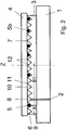
- FIG 2 A receiving device consisting of a carrier 1 and a receiving body 3 fixed on the carrier 1 is shown.
- the carrier 1 can be used, for example, for receiving by a robot arm or a process station and is therefore preferably made of rigid material, in particular metal.
- the carrier 1 advantageously has a larger base area than the receiving body 3.
- the receiving body 3 is made of a softer material than the carrier 1.
- the soft material can be, for example, Viton, silicone, rubber, NBR (nitrile rubbers), neoprene, etc.
- the semiconductor substrate 4 with its topography 5 can be received on a receiving side 7 of the receiving body 3 facing away from the carrier 1.
- the semiconductor substrate 4 can also have the topography 5 directed upwards, ie away from the receiving side 7.
- the receiving body 3 is penetrated by a vacuum channel 2, which extends further through the carrier 1 to a vacuum device (not shown) for applying a vacuum to a suction end 8 arranged on the receiving side 7.
- a plurality of vacuum channels 2 can be arranged distributed over the receiving body 3. It is advantageous to arrange the vacuum channel 2 or the suction end 8 outside a center Z of the receiving body 3. It is particularly advantageous if the distance B1 from the center Z to the suction end 8 is greater than the distance B2 from the suction end 8 to a circumference 9 of the receiving body 3.
- a ratio B1: B2 of 1.5: 1 to 3: 1, preferably 2: 1, is particularly advantageous.
- the suction end 8 is arranged in a depression 10 of the suction structure 6 and the depressions 10 are formed by elevations 11 forming the suction structure 6.
- the elevations 11 are tooth-like in the present case, the depressions 10 and elevations 11 being formed by a spiral path 12 starting in the center Z.
- the spiral path 12 forms the defined suction structure 6 and the spiral structure achieves a high flow resistance from the center Z to the circumference 9, which ensures a stable suction of the semiconductor substrate 4 on the receiving body 3.
- the bumps 5b can be received in the depressions 10 of the web 12.
- Figure 3 shows an enlarged section of the receiving body 3.
- Side walls S1, S2 of the recesses 10 are opposite one through the The receiving side 7 of the receiving body 3 formed angled receiving plane A, namely at the same angle with the identical angles W1, W2 in the exemplary embodiment between the side walls S1, S2 and the receiving plane A.
- the angles W1, W2 are between 30 ° and 85 °, preferably between 40 ° and 75 °.
- Elevations 11 shown in a pointed manner can be rounded off in an advantageous embodiment of the invention.
- a particular advantage of the invention also lies in the fact that different semiconductor substrates, in particular also different semiconductor substrates 4 with different diameters, can be picked up safely and gently with one and the same receiving device.
- Semiconductor substrates 4 which have essentially the same outer contour and / or the same outer circumference and / or the same diameter as the receiving body 3 are picked up particularly securely and gently.
Landscapes
- Engineering & Computer Science (AREA)
- Mechanical Engineering (AREA)
- Container, Conveyance, Adherence, Positioning, Of Wafer (AREA)
- Jigs For Machine Tools (AREA)
- Gripping Jigs, Holding Jigs, And Positioning Jigs (AREA)
- Constituent Portions Of Griding Lathes, Driving, Sensing And Control (AREA)
- Manipulator (AREA)
Description
- Die Erfindung betrifft eine Aufnahmeeinrichtung gemäß Anspruch 1.
- Eine präzise und positionstreue Fixierung von Halbleitersubstraten ist für eine Vielzahl von Prozessen in der Halbleiterindustrie unumgänglich. Zur Handhabung solcher Halbleitersubstrate werden die meist sehr dünnen und anfälligen Halbleitersubstrate auf eine Aufnahmeeinrichtung, einen sogenannten Chuck, aufgebracht und dort fixiert. Die für die Fixierung von Halbleitersubstraten auf den Chucks bekannten Technologien sind insbesondere bei extrem dünnen Halbleitersubstraten mit einer Dicke von weniger als 100 µm, insbesondere weniger als 50 µm sowie bei Substraten mit einer Topographie nicht anwendbar.
- Aufnahmeeinrichtungen sind in den Druckschriften
US 5 671 910 A , -
WO 2008/130173 A1 ,US 6 032 715 A ,WO 2004/011953 A1 und derWO 01/90820 A1 US 5 671 910 A offenbart ein Vakuumplattensystem mit einer Trägerplatte, die aus einer Vielzahl von Trägerplattenmodulen gebildet ist. - Eine sehr häufig verwendete Art der Fixierung erfolgt mit Hilfe von Vakuum beziehungsweise Unterdruck, wobei ein planes Halbleitersubstrat auf einer planen, gehärteten Oberfläche, in welche Vakuumbahnen gefräst sind, durch Unterdruck beziehungsweise Vakuum fixiert wird. Bei besonders dünnen Halbleitersubstraten können die Halbleitersubstrate entlang der Vakuumbahnen brechen oder zumindest beschädigt werden.
- Ein noch größeres Problem stellt die Fixierung von Substraten mit sehr hoher Topographie dar, wobei die Topographie beispielsweise durch sogenannte Bumps erzeugt wird. Bumps sind kugel-, kegel- oder prismenförmig (quader) aufgetragene, leitende Materialien, die später zur elektrischen Kontaktierung von weiteren Bauteilen dienen. Die Bumps können eine Höhe von mehr als 500 µm, typischerweise zwischen 4-200 µm, meist zwischen 10-150 µm, aufweisen und in einer großen Vielzahl über die gesamte Substratfläche verteilt sein. Daraus folgt, dass eine Fixierung des Halbleitersubstrats mit den bekannten Verfahren nicht in ausreichendem Maße möglich ist.
- Eine weitere Möglichkeit besteht in einer elektrostatischen Fixierung. Elektrostatische Fixiervorrichtungen haben jedoch den Nachteil, dass durch den Aufbau von elektrischen Feldern eine Beschädigung der komplexen Schaltungen auf den Halbleitersubstraten wahrscheinlich ist.
- Es ist daher die Aufgabe der vorliegenden Erfindung, eine Aufnahmeeinrichtung zu schaffen, mit der dünne Halbleitersubstrate sowie Halbleitersubstrate mit einer Topographie sicher und auf schonende Art und Weise aufgenommen und fixiert werden können.
- Diese Aufgabe wird mit den Merkmalen des Anspruchs 1 gelöst. Vorteilhafte Weiterbildungen der Erfindung sind in den Unteransprüchen angegeben.
- Der Erfindung liegt der Gedanke zugrunde, eine gattungsgemäße Aufnahmeeinrichtung durch Vorsehen einer definierten Saugstruktur auf einer Aufnahmeseite der Aufnahmeeinrichtung bei gleichzeitiger Verwendung eines weichen Oberflächenmaterials beziehungsweise Materials der Saugstruktur zu verbessern. Durch Vorsehen eines nachgiebigen Materials an der das Halbleitersubstrat kontaktierenden Oberfläche kann eine schonende Aufnahme des Halbleitersubstrats, auch bei Vorhandensein von einer Topographie auf dem Halbleitersubstrat, gewährleistet werden. Indem das weiche Material gleichzeitig eine das Halbleitersubstrat ansaugende Saugstruktur aufweist, werden die aus dem Stand der Technik bekannten Nachteile vermieden und eine sichere und schonende Aufnahme von dünnen und/oder mit einer Topographie versehenen Halbleitersubstraten ist möglich.
- Der Abstand zwischen benachbarten Erhebungen der Saugstruktur sollte dabei im Verhältnis zur Dicke des Halbleitersubstrats kleiner 1:7, insbesondere kleiner 1:5, bevorzugt kleiner 1:3, noch bevorzugter kleiner 1:2 sein. Analog gilt dies für Durchmesser etwaiger Topographien auf dem Halbleitersubstrat. Der Abstand zwischen benachbarten Erhebungen der Saugstruktur ist demnach maximal 7-fach im Vergleich zur Dicke des Halbleitersubstrats und/oder zum Durchmesser einzelner Topographien des auf der Aufnahmeeinrichtung aufzunehmenden Halbleitersubstrats.
- In einer vorteilhaften Ausgestaltung der Erfindung ist vorgesehen, dass sich die Saugstruktur über die gesamte Aufnahmeseite erstreckt. Somit ist das gesamte Halbleitersubstrats auf schonende Art und Weise aufnehmbar.
- Weiterhin ist mit Vorteil vorgesehen, dass die Saugstruktur eine Shorehärte von weniger als 90 Shore-A aufweist. Optimal für die einerseits stabile und andererseits schonende Halterung des Halbleitersubstrats ist ein weiches Material mit einer Shorehärte zwischen 10 Shore-A und 70 Shore-A, da auf das Halbleitersubstrat zum Teil hohe Auflage- und/oder Querkräfte wirken können. Außerdem ist es für eine hochgenaue Positionierung des Halbleitersubstrats erforderlich, dass das Halbleitersubstrat auf der Aufnahmeeinrichtung nicht schwimmt. Es hat sich jedoch überraschend herausgestellt, dass die Kombination aus weichem Material und Unterdruck auch für eine stabile Seitenführung beziehungsweise stabile Seitenfixierung Sorge trägt.
- Indem der Aufnahmekörper aus dem weichen Material besteht, kann der Aufnahmekörper mit der Saugstruktur erfindungsgemäß als ein Teil gebildet sein.
- Soweit die definierte Saugstruktur eine oder mehrere, insbesondere überwiegend in Umfangsrichtung des Aufnahmekörpers und/oder des Halbleitersubstrats verlaufende, Bahn(en) aufweist, lässt sich ein besonders definierter Unterdruck über die gesamte Fläche des Halbleitersubstrats aufbauen. Außerdem reicht durch die überwiegend in Umfangsrichtung des Aufnahmekörpers ausgerichteten Bahnen bereits ein geringfügiger Unterdruck aus, um das Halbleitersubstrat sicher zu fixieren.
- In einer weiteren vorteilhaften Ausführungsform der Erfindung ist vorgesehen, dass die Saugstruktur, insbesondere im Querschnitt benachbarter Bahnen, zahnartig ausgebildet ist.
- Mit Vorteil ist weiterhin vorgesehen, dass mindestens eine, insbesondere aus Erhebungen und Vertiefungen bestehende, Bahn spiralförmig, insbesondere von einem Zentrum Z des Aufnahmekörpers aus, verläuft. Eine spiralförmige Bahn lässt sich herstellungstechnisch einerseits leicht verwirklichen und andererseits wird ein maximaler Weg vom Zentrum der Aufnahmeeinrichtung bis zum Umfang der Aufnahmeeinrichtung verwirklicht, so dass ein optimaler Verlauf des an der Bahn anliegenden Unterdrucks gewährleistet ist.
- Indem das weiche Material erfindungsgemäß elektrisch leitend ausgebildet ist, können etwaige elektrostatische Aufladungen vermieden werden, beispielsweise durch Erdung der Aufnahmeeinrichtung.
- Gemäß einer weiteren vorteilhaften Ausführungsform der Erfindung ist vorgesehen, dass die Aufnahmeseite eine Aufnahmeebene A bildet und Seitenwände der Vertiefungen zur Aufnahmeebene A, insbesondere gleichwinkelig, angewinkelt sind, insbesondere in zwischen 30° und 85°, vorzugsweise zwischen 50° und 70°, liegenden Winkeln W1/W2. Der Winkel W1 gilt für eine erste Seitenwand der Vertiefung und der Winkel W2 für eine zweite Seitenwand der Vertiefung.
- Dabei ist es von besonderem Vorteil, wenn die Saugstruktur Topographien des Halbleitersubstrats durch die Elastizität und Geometrie der Saugstruktur aufnehmend ausgebildet ist.
- Weitere Vorteile, Merkmale und Einzelheiten der Erfindung ergeben sich aus der nachfolgenden Beschreibung bevorzugter Ausführungsbeispiele sowie anhand der Zeichnungen; diese zeigen in:
- Fig. 1:
- eine mikroskopische Aufnahme einer auf einem Halbleitersubstrat 4 aufgebrachten Topographie 5 und
- Fig. 2:
- eine schematische Darstellung der erfindungsgemäßen Aufnahmeeinrichtung und
- Fig. 3:
- einen schematischen Ausschnitt aus der erfindungsgemäßen Saugstruktur aus weichem Material.
- In den Figuren sind gleiche Bauteile und Bauteile mit der gleichen Funktion mit den gleichen Bezugszeichen gekennzeichnet.
-
Figur 1 zeigt einen Ausschnitt eines Halbleitersubstrats 4 mit einer Topographie 5, nämlich einzelnen Bumps 5b, die auf der Oberfläche des Halbleitersubstrats 4 verteilt angeordnet sind. - In
Figur 2 ist eine Aufnahmeeinrichtung bestehend aus einem Träger 1 und einem auf dem Träger 1 fixierten Aufnahmekörper 3 dargestellt. Der Träger 1 kann beispielsweise zur Aufnahme durch einen Roboterarm oder eine Prozessstation dienen und ist daher vorzugsweise aus starrem Material, insbesondere Metall, gebildet. Der Träger 1 weist mit Vorteil eine größere Grundfläche als der Aufnahmekörper 3 auf. Der Aufnahmekörper 3 ist gegenüber dem Träger 1 aus einem weicheren Material gebildet. Das weiche Material kann beispielsweise Viton, Silikon, Gummi, NBR (Nitrilkautschuke), Neoprene etc. sein. - Auf einer vom Träger 1 abgewandten Aufnahmeseite 7 des Aufnahmekörpers 3 ist das Halbleitersubstrat 4 mit seiner Topographie 5 aufnehmbar. Das Halbleitersubstrat 4 kann auch mit der Topographie 5 nach oben gerichtet, also von der Aufnahmeseite 7 weg, aufgenommen werden.
- Der Aufnahmekörper 3 ist von einem Unterdruckkanal 2 durchsetzt, der sich weiter durch den Träger 1 bis zu einer nicht dargestellten Vakuumeinrichtung zum Anlegen eines Vakuums an einem auf der Aufnahmeseite 7 angeordneten Saugende 8 erstreckt. Erfindungsgemäß können mehrere Unterdruckkanäle 2 verteilt über den Aufnahmekörper 3 angeordnet sein. Von Vorteil ist eine Anordnung des Unterdruckkanals 2 beziehungsweise des Saugendes 8 außerhalb eines Zentrums Z des Aufnahmekörpers 3. Besonders vorteilhaft ist es, wenn der Abstand B1 vom Zentrum Z zum Saugende 8 größer ist als der Abstand B2 vom Saugende 8 zu einem Umfang 9 des Aufnahmekörpers 3. Besonders vorteilhaft ist ein Verhältnis B1:B2 von 1,5:1 bis 3:1, vorzugsweise 2:1.
- Das Saugende 8 ist in einer Vertiefung 10 der Saugstruktur 6 angeordnet und den Vertiefungen 10 sind die Saugstruktur 6 ausbildende Erhebungen 11 benachbart. Die Erhebungen 11 sind im vorliegenden Fall zahnartig, wobei die Vertiefungen 10 und Erhebungen 11 durch eine im Zentrum Z beginnende spiralförmige Bahn 12 gebildet sind. Die spiralförmige Bahn 12 bildet die definierte Saugstruktur 6 und durch die Spiralstruktur wird ein hoher Strömungswiderstand vom Zentrum Z zum Umfang 9 erreicht, der für ein stabiles Ansaugen des Halbleitersubstrats 4 an dem Aufnahmekörper 3 Sorge trägt.
- In den Vertiefungen 10 der Bahn 12 sind die Bumps 5b aufnehmbar.
-
Figur 3 zeigt einen vergrößerten Ausschnitt des Aufnahmekörpers 3. Seitenwände S1, S2 der Vertiefungen 10 sind gegenüber einer durch die Aufnahmeseite 7 des Aufnahmekörpers 3 gebildeten Aufnahmeebene A angewinkelt, und zwar gleichwinklig mit den im Ausführungsbeispiel identischen Winkeln W1, W2 zwischen den Seitenwänden S1, S2 und der Aufnahmeebene A. Die Winkel W1, W2 liegen zwischen 30° und 85°, vorzugsweise zwischen 40° und 75°. - Die in
Figur 3 spitz dargestellten Erhebungen 11 können in einer vorteilhaften Ausführungsform der Erfindung abgerundet sein. - Ein besonderer Vorteil der Erfindung liegt außerdem darin, dass mit ein und derselben Aufnahmeeinrichtung verschiedene Halbleitersubstrate, insbesondere auch im Durchmesser verschiedene Halbleitersubstrate 4 sicher und schonend aufgenommen werden können.
- Besonders sicher und schonend werden Halbleitersubstrate 4 aufgenommen, die im Wesentlichen dieselbe Außenkontur und/oder denselben Außenumfang und/oder denselben Durchmesser wie der Aufnahmekörper 3 aufweisen.
-
- 1
- Träger
- 2
- Unterdruckkanal
- 3
- Aufnahmekörper
- 4
- Halbleitersubstrat
- 5
- Topographie
- 5b
- Bumps
- 6
- Saugstruktur
- 7
- Aufnahmeseite
- 8
- Saugende
- 9
- Umfang
- 10
- Vertiefungen
- 11
- Erhebungen
- 12
- Bahn
- S1/S2
- Seitenwände
- Z
- Zentrum
- A
- Aufnahmeebene
- W1
- Winkel
- W2
- Winkel
- B1
- Abstand
- B2
- Abstand
Claims (8)
- Aufnahmeeinrichtung zur Aufnahme von flächigen Halbleitersubstraten (4) mit- einem Träger (1),- einem auf dem Träger (1) fixierten oder fixierbaren Aufnahmekörper (3) mit einer vom Träger (1) abgewandten Aufnahmeseite (7) und- mindestens einem den Aufnahmekörper (3) durchsetzenden Unterdruckkanal (2) mit einem Saugende an der Aufnahmeseite (7), wobei die Aufnahmeseite (7) eine das Halbleitersubstrat (4) bei Anliegen von Unterdruck am Unterdruckkanal (2) ansaugende, definierte Saugstruktur (6) aus weichem Material aufweist,wobei
der Aufnahmekörper (3) aus dem weichen Material besteht und mit der Saugstruktur als ein Teil ausgebildet ist, dadurch gekennzeichnet, dass das weiche Material elektrisch leitend ausgebildet ist, um elektrostatische Aufladungen zu vermeiden. - Aufnahmeeinrichtung nach Anspruch 1,
dadurch gekennzeichnet,
dass sich die Saugstruktur (6) über die gesamte Aufnahmeseite (7) erstreckt. - Aufnahmeeinrichtung nach einem der vorhergehenden Ansprüche,
dadurch gekennzeichnet,
dass die Saugstruktur (6) eine Shore-Härte von weniger als 90 Shore-A aufweist - Aufnahmeeinrichtung nach einem der vorhergehenden Ansprüche,
dadurch gekennzeichnet,
dass die definierte Saugstruktur (6) eine oder mehrere, insbesondere überwiegend in Umfangsrichtung des Aufnahmekörpers (3) und/oder des Halbleitersubstrates verlaufende, Bahn(en) (12) aufweist. - Aufnahmeeinrichtung nach einem der vorhergehenden Ansprüche,
dadurch gekennzeichnet,
dass die Saugstruktur (6), insbesondere im Querschnitt benachbarter Bahnen (12), zahnartig ausgebildet ist. - Aufnahmeeinrichtung nach einem der vorhergehenden Ansprüche,
dadurch gekennzeichnet,
dass mindestens eine aus Erhebungen (11) und Vertiefungen (10) bestehende Bahn (12) spiralförmig, insbesondere von einem Zentrum (Z) des Aufnahmekörpers (3) aus, verläuft. - Aufnahmeeinrichtung nach einem der vorhergehenden Ansprüche,
dadurch gekennzeichnet,
dass die Aufnahmeseite (7) eine Aufnahmeebene A bildet und Seitenwände (S1/S2) der Vertiefungen (10) zur Aufnahmeebene A, insbesondere gleichwinklig, angewinkelt sind, insbesondere in zwischen 30° und 85°, vorzugsweise zwischen 40° und 75°, liegenden Winkeln W1/W2. - Aufnahmeeinrichtung nach Anspruch 7,
dadurch gekennzeichnet,
dass die Saugstruktur (6) Topographien (5) des Halbleitersubstrats (4) aufnehmend ausgebildet ist.
Applications Claiming Priority (2)
| Application Number | Priority Date | Filing Date | Title |
|---|---|---|---|
| DE102009018434.1A DE102009018434B4 (de) | 2009-04-22 | 2009-04-22 | Aufnahmeeinrichtung zur Aufnahme von Halbleitersubstraten |
| PCT/EP2010/002052 WO2010121701A1 (de) | 2009-04-22 | 2010-03-31 | Aufnahmeeinrichtung zur aufnahme von halbleitersubstraten |
Publications (2)
| Publication Number | Publication Date |
|---|---|
| EP2421677A1 EP2421677A1 (de) | 2012-02-29 |
| EP2421677B1 true EP2421677B1 (de) | 2020-05-27 |
Family
ID=42154433
Family Applications (1)
| Application Number | Title | Priority Date | Filing Date |
|---|---|---|---|
| EP10712715.1A Active EP2421677B1 (de) | 2009-04-22 | 2010-03-31 | Aufnahmeeinrichtung zur aufnahme von halbleitersubstraten |
Country Status (8)
| Country | Link |
|---|---|
| US (1) | US9278433B2 (de) |
| EP (1) | EP2421677B1 (de) |
| JP (2) | JP2012524984A (de) |
| KR (2) | KR101875351B1 (de) |
| CN (1) | CN102427916B (de) |
| DE (1) | DE102009018434B4 (de) |
| TW (1) | TWI511228B (de) |
| WO (1) | WO2010121701A1 (de) |
Families Citing this family (6)
| Publication number | Priority date | Publication date | Assignee | Title |
|---|---|---|---|---|
| KR101168863B1 (ko) * | 2009-02-23 | 2012-07-30 | 가부시키가이샤 소딕 | 착색 세라믹 진공 척 및 그 제조 방법 |
| JP5361634B2 (ja) * | 2009-09-25 | 2013-12-04 | 信越ポリマー株式会社 | 半導体ウェーハ用チャックテーブル及び半導体ウェーハの加工方法 |
| JP5657365B2 (ja) * | 2010-12-09 | 2015-01-21 | Udトラックス株式会社 | エアブラスト装置の搬送テーブル |
| DE102013100563A1 (de) * | 2013-01-21 | 2014-07-24 | Ev Group E. Thallner Gmbh | Aufnahmeeinrichtung zur Handhabung strukturierter Substrate |
| US11613869B2 (en) | 2015-10-05 | 2023-03-28 | Terminator Ip Limited | Reciprocating impact hammer |
| WO2017203067A1 (es) * | 2016-05-25 | 2017-11-30 | Zayer, S.A. | Utillaje para el mecanizado de piezas con curvatura |
Citations (1)
| Publication number | Priority date | Publication date | Assignee | Title |
|---|---|---|---|---|
| JP3312163B2 (ja) * | 1994-11-18 | 2002-08-05 | 日本電信電話株式会社 | 真空吸着装置 |
Family Cites Families (53)
| Publication number | Priority date | Publication date | Assignee | Title |
|---|---|---|---|---|
| US3307819A (en) * | 1965-04-12 | 1967-03-07 | Cocito Joe Michael | Disc valve for vacuum board |
| US4448404A (en) * | 1980-11-18 | 1984-05-15 | Nippon Kogaku K. K. | Device for holding a sheet-like sample |
| JPS5785235A (en) * | 1980-11-18 | 1982-05-27 | Nippon Kogaku Kk <Nikon> | Sampling stand |
| DE8703223U1 (de) * | 1987-03-03 | 1987-04-16 | Modellbau Paul Apitz, 7913 Senden | Vakuum-Spannplatte |
| JPH01258243A (ja) * | 1988-04-08 | 1989-10-16 | Fujitsu Ltd | 互換型書き換え可能光ディスク |
| FR2631165B1 (fr) * | 1988-05-05 | 1992-02-21 | Moulene Daniel | Support conditionneur de temperature pour petits objets tels que des composants semi-conducteurs et procede de regulation thermique utilisant ce support |
| JPH04152512A (ja) | 1990-10-16 | 1992-05-26 | Fujitsu Ltd | ウエハチャック |
| US5293370A (en) * | 1991-01-16 | 1994-03-08 | Del Mar Avionics | Method and apparatus for creating optical disc masters |
| AU4268193A (en) * | 1992-05-06 | 1993-11-29 | Carne, Charles Nicholas | Vacuum plates |
| JPH06120319A (ja) | 1992-10-08 | 1994-04-28 | Hitachi Ltd | 半導体製造装置 |
| US5738165A (en) * | 1993-05-07 | 1998-04-14 | Nikon Corporation | Substrate holding apparatus |
| JPH08288190A (ja) * | 1995-04-19 | 1996-11-01 | Hitachi Ltd | 物品取扱部材およびその製造方法および収納容器ならびに物品取扱装置 |
| JP2904086B2 (ja) * | 1995-12-27 | 1999-06-14 | 日本電気株式会社 | 半導体装置およびその製造方法 |
| US5923408A (en) * | 1996-01-31 | 1999-07-13 | Canon Kabushiki Kaisha | Substrate holding system and exposure apparatus using the same |
| JPH1022184A (ja) * | 1996-06-28 | 1998-01-23 | Sony Corp | 基板張り合わせ装置 |
| JPH10321708A (ja) | 1997-05-15 | 1998-12-04 | Sony Corp | 露光装置のウエハステージ |
| DE19722679A1 (de) * | 1997-05-30 | 1998-12-03 | Wacker Siltronic Halbleitermat | Scheibenhalter und Verfahren zur Herstellung einer Halbleiterscheibe |
| JPH1140646A (ja) * | 1997-07-18 | 1999-02-12 | Fujitsu Ltd | ピックアップツール |
| US6173648B1 (en) * | 1997-10-24 | 2001-01-16 | Sharp Kabushiki Kaisha | Manufacturing method of liquid crystal display element and manufacturing apparatus of the same |
| SG71182A1 (en) * | 1997-12-26 | 2000-03-21 | Canon Kk | Substrate processing apparatus substrate support apparatus substrate processing method and substrate manufacturing method |
| US6328096B1 (en) * | 1997-12-31 | 2001-12-11 | Temptronic Corporation | Workpiece chuck |
| US6073681A (en) * | 1997-12-31 | 2000-06-13 | Temptronic Corporation | Workpiece chuck |
| US6583638B2 (en) * | 1999-01-26 | 2003-06-24 | Trio-Tech International | Temperature-controlled semiconductor wafer chuck system |
| US6271676B1 (en) * | 1999-03-02 | 2001-08-07 | Tsk America, Inc. | Spiral chuck |
| US6182957B1 (en) * | 1999-08-12 | 2001-02-06 | International Business Machines Corporation | Apparatus and method for holding a flexible product in a flat and secure position |
| EP1077393A2 (de) * | 1999-08-19 | 2001-02-21 | Canon Kabushiki Kaisha | System zum Anziehen und Halten eines Substrats zur Verwendung in einem Belichtungsapparat |
| WO2004011953A1 (en) | 2000-03-15 | 2004-02-05 | Tsk America, Inc. | Spiral chuck |
| US6922387B1 (en) * | 2000-03-24 | 2005-07-26 | Matsushita Electric Industrial Co., Ltd. | Optical information recording medium, and method and apparatus for recording/reproducing information thereon |
| US6754143B2 (en) * | 2000-03-24 | 2004-06-22 | Matsushita Electric Industrial Co., Ltd. | Optical information recording medium, and method and apparatus for recording/reproducing information thereon |
| US6556281B1 (en) * | 2000-05-23 | 2003-04-29 | Asml Us, Inc. | Flexible piezoelectric chuck and method of using the same |
| JP2004505443A (ja) * | 2000-07-10 | 2004-02-19 | テンプトロニック コーポレイション | 交互配置された加熱および冷却要素と交換可能な上面アセンブリと硬膜層表面とをもつ熱プレートを有するウェーハチャック |
| JP4546626B2 (ja) * | 2000-08-29 | 2010-09-15 | 株式会社ディスコ | 半導体素子のピックアップ方法 |
| JP2002298343A (ja) * | 2001-03-28 | 2002-10-11 | Nec Corp | 光ディスクの記録再生方法および記録再生装置 |
| JP2002351082A (ja) * | 2001-05-24 | 2002-12-04 | Adtec Engineeng Co Ltd | 露光装置用基板ステージ |
| DE60217587D1 (de) * | 2001-07-26 | 2007-03-08 | Canon Kk | Substrathalter und ein Belichtungsapparat |
| JP4333065B2 (ja) | 2001-11-14 | 2009-09-16 | レーザーテック株式会社 | 基板保持装置 |
| JP2004259792A (ja) * | 2003-02-25 | 2004-09-16 | Nikon Corp | 吸着装置、吸着装置用シート、研磨装置、半導体デバイス及び半導体デバイス製造方法 |
| US7221553B2 (en) * | 2003-04-22 | 2007-05-22 | Applied Materials, Inc. | Substrate support having heat transfer system |
| JP3894562B2 (ja) * | 2003-10-01 | 2007-03-22 | キヤノン株式会社 | 基板吸着装置、露光装置およびデバイス製造方法 |
| US20050229854A1 (en) * | 2004-04-15 | 2005-10-20 | Tokyo Electron Limited | Method and apparatus for temperature change and control |
| JP4541824B2 (ja) * | 2004-10-14 | 2010-09-08 | リンテック株式会社 | 非接触型吸着保持装置 |
| JP2006305713A (ja) * | 2005-03-28 | 2006-11-09 | Nikon Corp | 吸着装置、研磨装置、半導体デバイス及び半導体デバイス製造方法 |
| US7136565B1 (en) * | 2005-05-23 | 2006-11-14 | Imation Corp. | Optical waveguide disk |
| JP4580327B2 (ja) * | 2005-11-21 | 2010-11-10 | 東京エレクトロン株式会社 | 被処理体の取り出し方法及びプログラム記憶媒体並びに載置機構 |
| JP2008085285A (ja) * | 2006-08-31 | 2008-04-10 | Fluoro Mechanic Kk | 真空ピンセット |
| JP2008066607A (ja) * | 2006-09-11 | 2008-03-21 | Tokyo Ohka Kogyo Co Ltd | 真空吸着装置 |
| JP5059450B2 (ja) * | 2007-03-06 | 2012-10-24 | 東京エレクトロン株式会社 | 基板載置台及び基板処理装置 |
| JP4746579B2 (ja) * | 2007-03-29 | 2011-08-10 | シャープ株式会社 | 低負荷搬送装置 |
| WO2008130173A1 (en) * | 2007-04-23 | 2008-10-30 | Hanmisemiconductor Co., Ltd | Suction pad for semiconductor package |
| JP5268345B2 (ja) * | 2007-12-20 | 2013-08-21 | パナソニック株式会社 | インダクタ |
| JP2011530833A (ja) * | 2008-08-12 | 2011-12-22 | アプライド マテリアルズ インコーポレイテッド | 静電チャックアセンブリ |
| KR101478414B1 (ko) * | 2009-07-16 | 2014-12-31 | 캐보트 마이크로일렉트로닉스 코포레이션 | 홈이 있는 cmp 연마 패드 |
| KR101059490B1 (ko) * | 2010-11-15 | 2011-08-25 | 테세라 리써치 엘엘씨 | 임베드된 트레이스에 의해 구성된 전도성 패드 |
-
2009
- 2009-04-22 DE DE102009018434.1A patent/DE102009018434B4/de active Active
-
2010
- 2010-03-31 CN CN201080017785.3A patent/CN102427916B/zh active Active
- 2010-03-31 KR KR1020177014327A patent/KR101875351B1/ko active Active
- 2010-03-31 WO PCT/EP2010/002052 patent/WO2010121701A1/de not_active Ceased
- 2010-03-31 JP JP2012506359A patent/JP2012524984A/ja active Pending
- 2010-03-31 KR KR1020117025691A patent/KR20120007017A/ko not_active Ceased
- 2010-03-31 EP EP10712715.1A patent/EP2421677B1/de active Active
- 2010-03-31 US US13/138,902 patent/US9278433B2/en active Active
- 2010-04-22 TW TW099112707A patent/TWI511228B/zh active
-
2014
- 2014-09-19 JP JP2014190883A patent/JP2015005778A/ja active Pending
Patent Citations (1)
| Publication number | Priority date | Publication date | Assignee | Title |
|---|---|---|---|---|
| JP3312163B2 (ja) * | 1994-11-18 | 2002-08-05 | 日本電信電話株式会社 | 真空吸着装置 |
Also Published As
| Publication number | Publication date |
|---|---|
| US9278433B2 (en) | 2016-03-08 |
| KR101875351B1 (ko) | 2018-07-05 |
| KR20120007017A (ko) | 2012-01-19 |
| TW201103100A (en) | 2011-01-16 |
| CN102427916B (zh) | 2016-08-03 |
| TWI511228B (zh) | 2015-12-01 |
| CN102427916A (zh) | 2012-04-25 |
| KR20170063973A (ko) | 2017-06-08 |
| DE102009018434B4 (de) | 2023-11-30 |
| EP2421677A1 (de) | 2012-02-29 |
| DE102009018434A1 (de) | 2010-10-28 |
| WO2010121701A1 (de) | 2010-10-28 |
| JP2012524984A (ja) | 2012-10-18 |
| JP2015005778A (ja) | 2015-01-08 |
| US20120146273A1 (en) | 2012-06-14 |
Similar Documents
| Publication | Publication Date | Title |
|---|---|---|
| DE69719882T2 (de) | Abtrennungsverfahren für Platten und Vorrichtung zur Durchführung dieses Verfahrens | |
| DE102009018434B4 (de) | Aufnahmeeinrichtung zur Aufnahme von Halbleitersubstraten | |
| DE19859467C2 (de) | Substrathalter | |
| WO2013023708A1 (de) | Vorrichtung und verfahren zum bonden von substraten | |
| AT519587B1 (de) | Saugvorrichtung für einen Endeffektor, Endeffektor zum Halten von Substraten sowie Verfahren zur Herstellung eines Endeffektors | |
| DE102009018156B4 (de) | Vorrichtung und Verfahren zum Trennen eines Substrats von einem Trägersubstrat | |
| WO2021209205A1 (de) | Beförderungsvorrichtung | |
| EP4381568A1 (de) | Vorrichtung und verfahren zur kontaktierung eines leiters | |
| DE10261306B4 (de) | Haltering mit reduzierter Abnutzungs- und Kontaminationsrate für einen Polierkopf einer CMP-Anlage und Polierkopf und CMP-Vorrichtung mit Haltering | |
| DE102010026610A1 (de) | Unterdruck-Saugeinheit und Greifer | |
| EP1435106B1 (de) | Hebe- und stützvorrichtung | |
| EP2659505B1 (de) | Verfahren und vorrichtung zum bonden zweier wafer | |
| DE102011005797A1 (de) | System zur Herstellung zahntechnischer Formteile | |
| EP2742527A1 (de) | Vorrichtung und verfahren zum bonden von substraten | |
| DE102019218444B4 (de) | Verfahren zur Herstellung einer Halbleitervorrichtung und Halbleitervorrichtung | |
| DE102023102601B4 (de) | Halbleiterscheibe und (Mikro-)Transferdruckverfahren | |
| EP3123503B1 (de) | Verfahren zur beschichtung von kavitäten eines halbleitersubstrats | |
| WO1999026287A1 (de) | Siliziumfolie als träger von halbleiterschaltungen als teil von karten | |
| EP2793314A1 (de) | Kontaktfeder und dessen Verwendung | |
| DE102020116083B3 (de) | Vorrichtung mit einem Werkstückträger zur Drucksinterverbindung eines ersten und zweiten Verbindungspartners und Verfahren zur Drucksinterverbindung dafür | |
| DE102005005124B4 (de) | Verfahren zur Ausrichtung einer Vielzahl von Substraten auf eine Belichtungsmaske | |
| EP1203398A1 (de) | Substrat und werkstückträger zur aufnahme des substrates | |
| DE102024125574A1 (de) | Elektrische Durchführung und Verfahren zu deren Herstellung | |
| WO2008152150A1 (de) | Herstellung von justagestrukturen fuer eine strukturierte schichtabscheidung auf einem wafer der mikrosystemtechnik | |
| DE102018208881B4 (de) | Verfahren und Vorrichtung zur Bestückung eines Trägers mit einem Bauteil |
Legal Events
| Date | Code | Title | Description |
|---|---|---|---|
| PUAI | Public reference made under article 153(3) epc to a published international application that has entered the european phase |
Free format text: ORIGINAL CODE: 0009012 |
|
| 17P | Request for examination filed |
Effective date: 20110929 |
|
| AK | Designated contracting states |
Kind code of ref document: A1 Designated state(s): AT BE BG CH CY CZ DE DK EE ES FI FR GB GR HR HU IE IS IT LI LT LU LV MC MK MT NL NO PL PT RO SE SI SK SM TR |
|
| DAX | Request for extension of the european patent (deleted) | ||
| 17Q | First examination report despatched |
Effective date: 20150922 |
|
| STAA | Information on the status of an ep patent application or granted ep patent |
Free format text: STATUS: EXAMINATION IS IN PROGRESS |
|
| GRAP | Despatch of communication of intention to grant a patent |
Free format text: ORIGINAL CODE: EPIDOSNIGR1 |
|
| STAA | Information on the status of an ep patent application or granted ep patent |
Free format text: STATUS: GRANT OF PATENT IS INTENDED |
|
| INTG | Intention to grant announced |
Effective date: 20200110 |
|
| GRAS | Grant fee paid |
Free format text: ORIGINAL CODE: EPIDOSNIGR3 |
|
| GRAA | (expected) grant |
Free format text: ORIGINAL CODE: 0009210 |
|
| STAA | Information on the status of an ep patent application or granted ep patent |
Free format text: STATUS: THE PATENT HAS BEEN GRANTED |
|
| AK | Designated contracting states |
Kind code of ref document: B1 Designated state(s): AT BE BG CH CY CZ DE DK EE ES FI FR GB GR HR HU IE IS IT LI LT LU LV MC MK MT NL NO PL PT RO SE SI SK SM TR |
|
| REG | Reference to a national code |
Ref country code: GB Ref legal event code: FG4D Free format text: NOT ENGLISH |
|
| REG | Reference to a national code |
Ref country code: CH Ref legal event code: EP |
|
| REG | Reference to a national code |
Ref country code: DE Ref legal event code: R096 Ref document number: 502010016648 Country of ref document: DE |
|
| REG | Reference to a national code |
Ref country code: AT Ref legal event code: REF Ref document number: 1274079 Country of ref document: AT Kind code of ref document: T Effective date: 20200615 |
|
| REG | Reference to a national code |
Ref country code: LT Ref legal event code: MG4D |
|
| PG25 | Lapsed in a contracting state [announced via postgrant information from national office to epo] |
Ref country code: LT Free format text: LAPSE BECAUSE OF FAILURE TO SUBMIT A TRANSLATION OF THE DESCRIPTION OR TO PAY THE FEE WITHIN THE PRESCRIBED TIME-LIMIT Effective date: 20200527 Ref country code: NO Free format text: LAPSE BECAUSE OF FAILURE TO SUBMIT A TRANSLATION OF THE DESCRIPTION OR TO PAY THE FEE WITHIN THE PRESCRIBED TIME-LIMIT Effective date: 20200827 Ref country code: FI Free format text: LAPSE BECAUSE OF FAILURE TO SUBMIT A TRANSLATION OF THE DESCRIPTION OR TO PAY THE FEE WITHIN THE PRESCRIBED TIME-LIMIT Effective date: 20200527 Ref country code: GR Free format text: LAPSE BECAUSE OF FAILURE TO SUBMIT A TRANSLATION OF THE DESCRIPTION OR TO PAY THE FEE WITHIN THE PRESCRIBED TIME-LIMIT Effective date: 20200828 Ref country code: PT Free format text: LAPSE BECAUSE OF FAILURE TO SUBMIT A TRANSLATION OF THE DESCRIPTION OR TO PAY THE FEE WITHIN THE PRESCRIBED TIME-LIMIT Effective date: 20200928 Ref country code: SE Free format text: LAPSE BECAUSE OF FAILURE TO SUBMIT A TRANSLATION OF THE DESCRIPTION OR TO PAY THE FEE WITHIN THE PRESCRIBED TIME-LIMIT Effective date: 20200527 Ref country code: IS Free format text: LAPSE BECAUSE OF FAILURE TO SUBMIT A TRANSLATION OF THE DESCRIPTION OR TO PAY THE FEE WITHIN THE PRESCRIBED TIME-LIMIT Effective date: 20200927 |
|
| REG | Reference to a national code |
Ref country code: NL Ref legal event code: MP Effective date: 20200527 |
|
| PG25 | Lapsed in a contracting state [announced via postgrant information from national office to epo] |
Ref country code: HR Free format text: LAPSE BECAUSE OF FAILURE TO SUBMIT A TRANSLATION OF THE DESCRIPTION OR TO PAY THE FEE WITHIN THE PRESCRIBED TIME-LIMIT Effective date: 20200527 Ref country code: BG Free format text: LAPSE BECAUSE OF FAILURE TO SUBMIT A TRANSLATION OF THE DESCRIPTION OR TO PAY THE FEE WITHIN THE PRESCRIBED TIME-LIMIT Effective date: 20200827 Ref country code: LV Free format text: LAPSE BECAUSE OF FAILURE TO SUBMIT A TRANSLATION OF THE DESCRIPTION OR TO PAY THE FEE WITHIN THE PRESCRIBED TIME-LIMIT Effective date: 20200527 |
|
| PG25 | Lapsed in a contracting state [announced via postgrant information from national office to epo] |
Ref country code: NL Free format text: LAPSE BECAUSE OF FAILURE TO SUBMIT A TRANSLATION OF THE DESCRIPTION OR TO PAY THE FEE WITHIN THE PRESCRIBED TIME-LIMIT Effective date: 20200527 |
|
| PG25 | Lapsed in a contracting state [announced via postgrant information from national office to epo] |
Ref country code: EE Free format text: LAPSE BECAUSE OF FAILURE TO SUBMIT A TRANSLATION OF THE DESCRIPTION OR TO PAY THE FEE WITHIN THE PRESCRIBED TIME-LIMIT Effective date: 20200527 Ref country code: SM Free format text: LAPSE BECAUSE OF FAILURE TO SUBMIT A TRANSLATION OF THE DESCRIPTION OR TO PAY THE FEE WITHIN THE PRESCRIBED TIME-LIMIT Effective date: 20200527 Ref country code: RO Free format text: LAPSE BECAUSE OF FAILURE TO SUBMIT A TRANSLATION OF THE DESCRIPTION OR TO PAY THE FEE WITHIN THE PRESCRIBED TIME-LIMIT Effective date: 20200527 Ref country code: CZ Free format text: LAPSE BECAUSE OF FAILURE TO SUBMIT A TRANSLATION OF THE DESCRIPTION OR TO PAY THE FEE WITHIN THE PRESCRIBED TIME-LIMIT Effective date: 20200527 Ref country code: ES Free format text: LAPSE BECAUSE OF FAILURE TO SUBMIT A TRANSLATION OF THE DESCRIPTION OR TO PAY THE FEE WITHIN THE PRESCRIBED TIME-LIMIT Effective date: 20200527 Ref country code: DK Free format text: LAPSE BECAUSE OF FAILURE TO SUBMIT A TRANSLATION OF THE DESCRIPTION OR TO PAY THE FEE WITHIN THE PRESCRIBED TIME-LIMIT Effective date: 20200527 |
|
| PG25 | Lapsed in a contracting state [announced via postgrant information from national office to epo] |
Ref country code: PL Free format text: LAPSE BECAUSE OF FAILURE TO SUBMIT A TRANSLATION OF THE DESCRIPTION OR TO PAY THE FEE WITHIN THE PRESCRIBED TIME-LIMIT Effective date: 20200527 Ref country code: SK Free format text: LAPSE BECAUSE OF FAILURE TO SUBMIT A TRANSLATION OF THE DESCRIPTION OR TO PAY THE FEE WITHIN THE PRESCRIBED TIME-LIMIT Effective date: 20200527 |
|
| REG | Reference to a national code |
Ref country code: DE Ref legal event code: R097 Ref document number: 502010016648 Country of ref document: DE |
|
| PLBE | No opposition filed within time limit |
Free format text: ORIGINAL CODE: 0009261 |
|
| STAA | Information on the status of an ep patent application or granted ep patent |
Free format text: STATUS: NO OPPOSITION FILED WITHIN TIME LIMIT |
|
| 26N | No opposition filed |
Effective date: 20210302 |
|
| PG25 | Lapsed in a contracting state [announced via postgrant information from national office to epo] |
Ref country code: SI Free format text: LAPSE BECAUSE OF FAILURE TO SUBMIT A TRANSLATION OF THE DESCRIPTION OR TO PAY THE FEE WITHIN THE PRESCRIBED TIME-LIMIT Effective date: 20200527 |
|
| PG25 | Lapsed in a contracting state [announced via postgrant information from national office to epo] |
Ref country code: MC Free format text: LAPSE BECAUSE OF FAILURE TO SUBMIT A TRANSLATION OF THE DESCRIPTION OR TO PAY THE FEE WITHIN THE PRESCRIBED TIME-LIMIT Effective date: 20200527 |
|
| REG | Reference to a national code |
Ref country code: CH Ref legal event code: PL |
|
| REG | Reference to a national code |
Ref country code: BE Ref legal event code: MM Effective date: 20210331 |
|
| PG25 | Lapsed in a contracting state [announced via postgrant information from national office to epo] |
Ref country code: CH Free format text: LAPSE BECAUSE OF NON-PAYMENT OF DUE FEES Effective date: 20210331 Ref country code: LI Free format text: LAPSE BECAUSE OF NON-PAYMENT OF DUE FEES Effective date: 20210331 Ref country code: LU Free format text: LAPSE BECAUSE OF NON-PAYMENT OF DUE FEES Effective date: 20210331 Ref country code: IE Free format text: LAPSE BECAUSE OF NON-PAYMENT OF DUE FEES Effective date: 20210331 |
|
| PG25 | Lapsed in a contracting state [announced via postgrant information from national office to epo] |
Ref country code: BE Free format text: LAPSE BECAUSE OF NON-PAYMENT OF DUE FEES Effective date: 20210331 |
|
| PG25 | Lapsed in a contracting state [announced via postgrant information from national office to epo] |
Ref country code: HU Free format text: LAPSE BECAUSE OF FAILURE TO SUBMIT A TRANSLATION OF THE DESCRIPTION OR TO PAY THE FEE WITHIN THE PRESCRIBED TIME-LIMIT; INVALID AB INITIO Effective date: 20100331 Ref country code: CY Free format text: LAPSE BECAUSE OF FAILURE TO SUBMIT A TRANSLATION OF THE DESCRIPTION OR TO PAY THE FEE WITHIN THE PRESCRIBED TIME-LIMIT Effective date: 20200527 |
|
| PG25 | Lapsed in a contracting state [announced via postgrant information from national office to epo] |
Ref country code: MK Free format text: LAPSE BECAUSE OF FAILURE TO SUBMIT A TRANSLATION OF THE DESCRIPTION OR TO PAY THE FEE WITHIN THE PRESCRIBED TIME-LIMIT Effective date: 20200527 |
|
| PG25 | Lapsed in a contracting state [announced via postgrant information from national office to epo] |
Ref country code: TR Free format text: LAPSE BECAUSE OF FAILURE TO SUBMIT A TRANSLATION OF THE DESCRIPTION OR TO PAY THE FEE WITHIN THE PRESCRIBED TIME-LIMIT Effective date: 20200527 |
|
| PG25 | Lapsed in a contracting state [announced via postgrant information from national office to epo] |
Ref country code: MT Free format text: LAPSE BECAUSE OF FAILURE TO SUBMIT A TRANSLATION OF THE DESCRIPTION OR TO PAY THE FEE WITHIN THE PRESCRIBED TIME-LIMIT Effective date: 20200527 |
|
| PGFP | Annual fee paid to national office [announced via postgrant information from national office to epo] |
Ref country code: IT Payment date: 20250331 Year of fee payment: 16 |
|
| PGFP | Annual fee paid to national office [announced via postgrant information from national office to epo] |
Ref country code: GB Payment date: 20260324 Year of fee payment: 17 |
|
| PGFP | Annual fee paid to national office [announced via postgrant information from national office to epo] |
Ref country code: DE Payment date: 20260320 Year of fee payment: 17 |
|
| PGFP | Annual fee paid to national office [announced via postgrant information from national office to epo] |
Ref country code: AT Payment date: 20260319 Year of fee payment: 17 |
|
| PGFP | Annual fee paid to national office [announced via postgrant information from national office to epo] |
Ref country code: FR Payment date: 20260324 Year of fee payment: 17 |