EP2399259B1 - Spin-transfer torque memory self-reference read method - Google Patents
Spin-transfer torque memory self-reference read method Download PDFInfo
- Publication number
- EP2399259B1 EP2399259B1 EP10707396.7A EP10707396A EP2399259B1 EP 2399259 B1 EP2399259 B1 EP 2399259B1 EP 10707396 A EP10707396 A EP 10707396A EP 2399259 B1 EP2399259 B1 EP 2399259B1
- Authority
- EP
- European Patent Office
- Prior art keywords
- resistance state
- tunnel junction
- magnetic tunnel
- data cell
- junction data
- Prior art date
- Legal status (The legal status is an assumption and is not a legal conclusion. Google has not performed a legal analysis and makes no representation as to the accuracy of the status listed.)
- Not-in-force
Links
- 238000000034 method Methods 0.000 title claims description 36
- 230000005291 magnetic effect Effects 0.000 claims description 88
- 230000007423 decrease Effects 0.000 claims description 6
- 230000005294 ferromagnetic effect Effects 0.000 description 22
- 238000010586 diagram Methods 0.000 description 14
- 230000005415 magnetization Effects 0.000 description 14
- 238000001514 detection method Methods 0.000 description 13
- 230000005290 antiferromagnetic effect Effects 0.000 description 4
- 230000003068 static effect Effects 0.000 description 4
- 230000004888 barrier function Effects 0.000 description 3
- 239000000463 material Substances 0.000 description 3
- 238000013500 data storage Methods 0.000 description 2
- 229910019041 PtMn Inorganic materials 0.000 description 1
- 229910045601 alloy Inorganic materials 0.000 description 1
- 239000000956 alloy Substances 0.000 description 1
- PNEYBMLMFCGWSK-UHFFFAOYSA-N aluminium oxide Inorganic materials [O-2].[O-2].[O-2].[Al+3].[Al+3] PNEYBMLMFCGWSK-UHFFFAOYSA-N 0.000 description 1
- 230000002457 bidirectional effect Effects 0.000 description 1
- 239000003990 capacitor Substances 0.000 description 1
- 238000004891 communication Methods 0.000 description 1
- 229910052593 corundum Inorganic materials 0.000 description 1
- 239000012777 electrically insulating material Substances 0.000 description 1
- -1 for example Substances 0.000 description 1
- 230000010354 integration Effects 0.000 description 1
- 230000000704 physical effect Effects 0.000 description 1
- 230000010287 polarization Effects 0.000 description 1
- 239000004065 semiconductor Substances 0.000 description 1
- 230000005641 tunneling Effects 0.000 description 1
- 239000013598 vector Substances 0.000 description 1
- 229910001845 yogo sapphire Inorganic materials 0.000 description 1
Images


Classifications
-
- G—PHYSICS
- G11—INFORMATION STORAGE
- G11C—STATIC STORES
- G11C11/00—Digital stores characterised by the use of particular electric or magnetic storage elements; Storage elements therefor
- G11C11/02—Digital stores characterised by the use of particular electric or magnetic storage elements; Storage elements therefor using magnetic elements
- G11C11/16—Digital stores characterised by the use of particular electric or magnetic storage elements; Storage elements therefor using magnetic elements using elements in which the storage effect is based on magnetic spin effect
- G11C11/165—Auxiliary circuits
- G11C11/1673—Reading or sensing circuits or methods
-
- G—PHYSICS
- G11—INFORMATION STORAGE
- G11C—STATIC STORES
- G11C11/00—Digital stores characterised by the use of particular electric or magnetic storage elements; Storage elements therefor
- G11C11/02—Digital stores characterised by the use of particular electric or magnetic storage elements; Storage elements therefor using magnetic elements
- G11C11/16—Digital stores characterised by the use of particular electric or magnetic storage elements; Storage elements therefor using magnetic elements using elements in which the storage effect is based on magnetic spin effect
Definitions
- Flash memory is one such device but has several drawbacks such as slow access speed ( ⁇ ms write and ⁇ 50-100ns read), limited endurance ( ⁇ 10 3 -10 4 programming cycles), and the integration difficulty in system-on-chip (SoC). Flash memory (NAND or NOR) also faces significant scaling problems at 32nm node and beyond.
- MRAM Magneto-resistive Random Access Memory
- MRAM Magneto-resistive Random Access Memory
- MRAM features non-volatility, fast writing/reading speed ( ⁇ 10ns), almost unlimited programming endurance (>10 15 cycles) and zero standby power.
- the basic component of MRAM is a magnetic tunneling junction (MTJ).
- MTJ magnetic tunneling junction
- Data storage is realized by switching the resistance of MTJ between a high-resistance state and a low-resistance state.
- MRAM switches the MTJ resistance by using a current induced magnetic field to switch the magnetization of MTJ. As the MTJ size shrinks, the switching magnetic field amplitude increases and the switching variation becomes more severe.
- STRAM Spin-Torque Transfer RAM
- MTJ Magnetization switching
- the switching mechanism of STRAM is constrained locally and STRAM is believed to have a better scaling property than the conventional MRAM.
- reading a STRAM cell is challenging as the cell is scaled down.
- US 2006/092734 discloses a read circuit of a semiconductor memory based on a self-reference sensing technique by which data stored in a memory cell is determined by first and second signals read out from a memory cell through first and second read operations.
- This read circuit includes a sense amplifier which determines the data stored in the memory cell based on a potential of an input node, a transfer transistor which is connected between the memory cell and the input node, a precharge circuit which sets the input node to a precharge potential, and a bias voltage generator which sets the transfer transistor cutoff based on the first signal.
- the present disclosure relates to spin-transfer torque random access memory self-preference read operations and apparatus for the same.
- present disclosure relates to a spin-transfer torque random access memory self-reference read operation.
- a magnetic memory apparatus as defined in claim 16.
- the present disclosure relates to spin-transfer torque memory apparatus and self-reference read methods.
- present disclosure relates to self-reference reading methods to determine whether a spin-transfer torque memory unit has a high resistance state or low resistance state data state.
- a read current or read voltage sufficient to switch the resistance state of a magnetic tunnel junction data cell, is applied to a magnetic tunnel junction data cell.
- a resulting read voltage or current is detected and if a voltage or current jump or drop is detected, the resistance state of the magnetic tunnel junction data cell is determined to be the opposing data state that the read current or read voltage was sufficient to switch the magnetic tunnel junction to.
- the resistance state of the magnetic tunnel junction data cell is determined to be the data state that the read current or read voltage was sufficient to switch the magnetic tunnel junction to. If a resulting read voltage or resulting read current jump or drop is detected, then a write back operation returns the magnetic tunnel junction data cell to its original resistive data state.
- the disclosed method provides a large available detection signal, and fast reading speed. While the present disclosure is not so limited, an appreciation of various aspects of the disclosure will be gained through a discussion of the examples provided below.
- FIG. 1 is a cross-sectional schematic diagram of an illustrative spin-transfer torque MTJ memory unit 10 in the low resistance state
- FIG. 2 is a cross-sectional schematic diagram of another spin-transfer torque MTJ memory unit 10 in the high resistance state.
- a magnetic tunnel junction (MTJ) memory unit 10 includes a ferromagnetic free layer 12 and a ferromagnetic reference (i.e., pinned) layer 14 .
- the ferromagnetic free layer 12 and a ferromagnetic reference layer 14 are separated by an oxide barrier layer 13 or tunnel barrier.
- a first electrode 15 is in electrical contact with the ferromagnetic free layer 12 and a second electrode 16 is in electrical contact with the ferromagnetic reference layer 14 .
- the ferromagnetic layers 12, 14 may be made of any useful ferromagnetic (FM) alloys such as, for example, Fe, Co, Ni and the insulating barrier layer 13 may be made of an electrically insulating material such as, for example an oxide material (e.g., Al 2 O 3 or MgO). Other suitable materials may also be used.
- FM ferromagnetic
- oxide material e.g., Al 2 O 3 or MgO
- the electrodes 15, 16 electrically connect the ferromagnetic layers 12, 14 to a control circuit providing read and write currents through the ferromagnetic layers 12, 14 .
- the resistance across the spin-transfer torque MTJ memory unit 10 is determined by the relative orientation of the magnetization vectors or magnetization orientations of the ferromagnetic layers 12, 14 .
- the magnetization direction of the ferromagnetic reference layer 14 is pinned in a predetermined direction while the magnetization direction of the ferromagnetic free layer 12 is free to rotate under the influence of a spin torque. Pinning of the ferromagnetic reference layer 14 may be achieved through, e.g., the use of exchange bias with an antiferromagnetically ordered material such as PtMn, IrMn and others.
- the reference magnetic layer 14 can be a single ferromagnetic layer, or may include multiple layers, for example, a pair of ferromagnetically coupled ferromagnetic layers, an antiferromagnetic pinning layer and a ferromagnetic pinned layer, a synthetic antiferromagnetic, or a synthetic antiferromagnetic with an antiferromagnetic layer.
- FIG. 1 illustrates the spin-transfer torque MTJ memory unit 10 in the low resistance state where the magnetization orientation of the ferromagnetic free layer 12 is parallel and in the same direction of the magnetization orientation of the ferromagnetic reference layer 14 . This is termed the low resistance state or "0"data state.
- FIG. 2 illustrates the spin-transfer torque MTJ memory unit 10 in the high resistance state where the magnetization orientation of the ferromagnetic free layer 12 is anti-parallel and in the opposite direction of the magnetization orientation of the ferromagnetic reference layer 14 . This is termed the high resistance state or "1"data state.
- the illustrative spin-transfer torque MTJ memory unit 10 may be used to construct a memory device that includes multiple MTJ memory units where a data bit is stored in spin-transfer torque MTJ memory unit by changing the relative magnetization state of the free magnetic layer 12 with respect to the pinned magnetic layer 14 .
- the stored data bit can be read out by measuring the resistance of the cell which changes with the magnetization direction of the free layer relative to the pinned magnetic layer.
- the free layer exhibits thermal stability against random fluctuations so that the orientation of the free layer is changed only when it is controlled to make such a change.
- This thermal stability can be achieved via the magnetic anisotropy using different methods, e.g., varying the bit size, shape, and crystalline anisotropy.
- the anisotropy causes a soft and hard axis to form in thin magnetic layers.
- the hard and soft axes are defined by the magnitude of the external energy, usually in the form of a magnetic field, needed to fully rotate (saturate) the direction of the magnetization in that direction, with the hard axis requiring a higher saturation magnetic field.
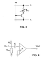
- FIG. 3 is a schematic diagram of an illustrative spin-transfer torque MTJ memory unit MTJ .
- the spin-transfer torque MTJ memory unit MTJ is electrically connected in series to a transistor such as, for example, a NMOS transistor.
- the opposing side of the spin-transfer torque MTJ memory unit MTJ is electrically connected to a bit line BL .
- the transistor is electrically coupled to a source line SL and a word line WL .
- the MTJ can be modeled as a variable resistor in circuit schematic, as shown in FIG. 3 .
- FIG. 4 is a schematic circuit diagram of an illustrative spin-transfer torque MTJ memory apparatus to detect a voltage (or current) jump or drop during the read operation described herein.
- the detection circuit can be described as a differentiator.
- the magnetic tunnel junction data cell R MTJ (as described above) is electrically connected to a current source I s (or voltage source Vs ) and a capacitor C is electrically between the magnetic tunnel junction data cell R MTJ and a sense amplifier A .
- the sense amplifier A provides a voltage output V OUT . Any voltage change can be detected by the differentiator.
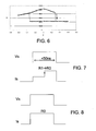
- An illustrative detailed signal is shown in FIG. 5 .
- FIG. 5 illustrates application of a constant current source I s and a corresponding resulting voltage drop V s .
- the voltage output V OUT show three voltage spikes.
- a clock CLOCK is utilized to remove the unwanted initial and final voltage spikes (at the start and end of the signal detection).
- the resulting voltage output V OUT1 indicates a voltage drop due to the magnetic tunnel junction data cell R MTJ switching resistance states (from the high resistance state to the low resistance state in this example).
- the read operation indicates that the magnetic tunnel junction data cell R MTJ was in the high resistance state.
- a write back operation can then be performed to return the magnetic tunnel junction data cell R MTJ to the original high resistance state.
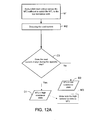
- FIG. 6 is a is a graph of a static R-V (resistance-voltage) curve of a spin-transfer torque MTJ memory unit where the resistance state switches from the high resistance state to the low resistance state.
- the MTJ 10 When applying a positive voltage on the second electrode 16 in FIG. 1 or 2 , the MTJ 10 enters the positive applied voltage region in FIG. 6 and switches from the high resistance state ( FIG. 2 ) to the low resistance state ( FIG. 1 ).
- the MTJ 10 When applying a positive voltage on the first electrode 15 in FIG. 1 or 2 , the MTJ 10 enters the negative applied voltage region in FIG. 6 .
- the resistance of the MTJ switches from the low resistance state ( FIG. 1 ) to the high resistance state ( FIG. 2 ).
- FIG. 7 is illustrative detailed signal timing graphs for read current detection at the high to low resistance state switching voltage when the spin-transfer torque MTJ memory unit is in the high resistance state.
- FIG. 8 is illustrative detailed signal timing graphs for read current detection at the high to low resistance state switching voltage when the spin-transfer torque MTJ memory unit is in the low resistance state.
- a read voltage Vs is applied across the magnetic tunnel junction data cell or spin-transfer torque MTJ memory unit.
- the read voltage Vs is equal to or greater than the critical voltage that is sufficient to switch the data resistance state of the magnetic tunnel junction data cell (from the high to the low resistance state in this example).
- the read voltage Vs is applied for a time duration of 0.1 to 50 nanoseconds, or from 0.1 to 25 nanoseconds, or from 01. to 10 nanoseconds.
- the read operation is a high speed operation.
- the resulting (or sensed) read current Is passing though the magnetic tunnel junction data cell is detected, as illustrated in FIG. 7 and FIG. 8.
- FIG. 7 illustrates the magnetic tunnel junction data cell in the high resistance state R1 and switching to the low resistance state R0 .
- FIG. 8 illustrates the magnetic tunnel junction data cell in the low resistance state R0 .
- a sensed read current Is remains constant during the read operation.
- the read voltage is equal to or greater than the critical voltage that is sufficient to switch the data resistance state of the magnetic tunnel junction data cell from the low to the high resistance state.
- FIG. 9 is a is a graph of a static R-I (resistance-current) curve of a spin-transfer torque MTJ memory unit where the resistance state switches from the high resistance state to the low resistance state.
- FIG. 10 is illustrative detailed signal timing graphs for read voltage detection at the high to low resistance state switching current when the spin-transfer torque MTJ memory unit is in the high resistance state.
- FIG. 11 is illustrative detailed signal timing graphs for read voltage detection at the high to low resistance state switching current when the spin-transfer torque MTJ memory unit is in the low resistance state.
- a read current Is is applied across the magnetic tunnel junction data cell or spin-transfer torque MTJ memory unit.
- the read current Is is equal to or greater than the critical current that is sufficient to switch the data resistance state of the magnetic tunnel junction data cell (from the high to the low resistance state in this example).
- the read current Is is applied for a time duration of 0.1 to 50 nanoseconds, or from 0.1 to 25 nanoseconds, or from 0.1 to 10 nanoseconds.
- the read operation is a high speed operation.
- the resulting (or sensed) read voltage Vs passing though the magnetic tunnel junction data cell is detected, as illustrated in FIG. 10 and FIG. 11.
- FIG. 10 illustrates the magnetic tunnel junction data cell in the high resistance state R1 and switching to the low resistance state R0 .
- a sensed read voltage Vs drop occurs during the read operation.
- the voltage change can be 100 mV or more.
- FIG. 11 illustrates the magnetic tunnel junction data cell in the low resistance state R0 .
- a sensed read voltage Vs remains constant during the read operation.
- the read current is equal to or greater than the critical current that is sufficient to switch the data resistance state of the magnetic tunnel junction data cell from the low to the high resistance state.
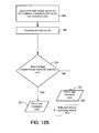
- FIG. 12A is a flow diagram of an illustrative self-reference reading method sensing a read current when applying a voltage sufficient to switch the MTJ from a high resistance state to a low resistance state.
- the method includes applying a read voltage across a magnetic tunnel junction data cell and forming a read current at block M1.
- the magnetic tunnel junction data cell having a first resistance state and the read voltage is sufficient to switch the magnetic tunnel junction data cell resistance (from the high to the low resistance state, in this example).
- the read current is detected.
- the method includes determining if the read current remains constant during the applying step at block C3.
- the first resistance state of the magnetic tunnel junction data cell is the resistance state that the read voltage was sufficient to switch the magnetic tunnel junction data cell to (the low resistance state, in this example) at block D2 . If the read current changes (increases, in this example) the first resistance state is the opposing resistance state (the high resistance state, in this example) at block D1 and the high resistance state is written back to the magnetic tunnel junction data cell at block M3 .
- FIG. 12B is a flow diagram of an illustrative self-reference reading method sensing a read current when applying a voltage sufficient to switch the MTJ from a low resistance state to a high resistance state.
- the method includes applying a read voltage across a magnetic tunnel junction data cell and forming a read current at block M4.
- the magnetic tunnel junction data cell having a first resistance state and the read voltage is sufficient to switch the magnetic tunnel junction data cell resistance (from the low to the high resistance state, in this example).
- the read current is detected.
- the method includes determining if the read current remains constant during the applying step at block C4 .
- the first resistance state of the magnetic tunnel junction data cell is the resistance state that the read voltage was sufficient to switch the magnetic tunnel junction data cell to (the high resistance state, in this example) at block D4 . If the read current changes (increases, in this example) the first resistance state is the opposing resistance state (the high resistance state, in this example) at block D3 and the low resistance state is written back to the magnetic tunnel junction data cell at block M6 .
- FIG. 13 is a flow diagram of an illustrative self-reference reading method sensing a read voltage.
- the method includes applying a read current across a magnetic tunnel junction data cell and forming a read voltage at block M11.
- the magnetic tunnel junction data cell having a first resistance state and the read current is sufficient to switch the magnetic tunnel junction data cell resistance (from the high to the low resistance state, in this example).
- the read voltage is detected.
- the method includes determining if the read voltage remains constant during the applying step at block C13 . If the read voltage remains constant during the applying step, then the first resistance state of the magnetic tunnel junction data cell is the resistance state that the read current was sufficient to switch the magnetic tunnel junction data cell to (the low resistance state, in this example) at block D12 . Otherwise the first resistance state is the opposing resistance state (the high resistance state, in this example) at block D11 and the high resistance state is written back to the magnetic tunnel junction data cell at block M13 .
- the read current is sufficient to switch the magnetic tunnel junction data cell resistance from the low to the high resistance state.
- the first resistance state of the magnetic tunnel junction data cell is the low resistance state. If the read voltage does not remain constant or changes (increases in this example) the first resistance state is the opposing resistance state (the high resistance state, in this example) and the high resistance state is written back to the magnetic tunnel junction data cell at block.
- embodiments of the SPIN-TRANSFER TORQUE MEMORY SELF-REFERENCE READ METHOD are disclosed. The implementations described above and other implementations are within the scope of the following claims. One skilled in the art will appreciate that the present disclosure can be practiced with embodiments other than those disclosed. The disclosed embodiments are presented for purposes of illustration and not limitation, and the present invention is limited only by the claims that follow.
Landscapes
- Engineering & Computer Science (AREA)
- Computer Hardware Design (AREA)
- Hall/Mr Elements (AREA)
- Mram Or Spin Memory Techniques (AREA)
Applications Claiming Priority (2)
| Application Number | Priority Date | Filing Date | Title |
|---|---|---|---|
| US12/390,006 US7876604B2 (en) | 2008-11-05 | 2009-02-20 | Stram with self-reference read scheme |
| PCT/US2010/024928 WO2010096768A1 (en) | 2009-02-20 | 2010-02-22 | Spin-transfer torque memory self-reference read method |
Publications (2)
| Publication Number | Publication Date |
|---|---|
| EP2399259A1 EP2399259A1 (en) | 2011-12-28 |
| EP2399259B1 true EP2399259B1 (en) | 2013-09-18 |
Family
ID=42173868
Family Applications (1)
| Application Number | Title | Priority Date | Filing Date |
|---|---|---|---|
| EP10707396.7A Not-in-force EP2399259B1 (en) | 2009-02-20 | 2010-02-22 | Spin-transfer torque memory self-reference read method |
Country Status (6)
| Country | Link |
|---|---|
| US (2) | US7876604B2 (enExample) |
| EP (1) | EP2399259B1 (enExample) |
| JP (1) | JP2012518867A (enExample) |
| KR (1) | KR101405863B1 (enExample) |
| CN (1) | CN102326204B (enExample) |
| WO (1) | WO2010096768A1 (enExample) |
Families Citing this family (13)
| Publication number | Priority date | Publication date | Assignee | Title |
|---|---|---|---|---|
| US7826255B2 (en) * | 2008-09-15 | 2010-11-02 | Seagate Technology Llc | Variable write and read methods for resistive random access memory |
| US7859891B2 (en) * | 2008-09-30 | 2010-12-28 | Seagate Technology Llc | Static source plane in stram |
| US7876604B2 (en) * | 2008-11-05 | 2011-01-25 | Seagate Technology Llc | Stram with self-reference read scheme |
| US9183911B2 (en) | 2011-11-17 | 2015-11-10 | Everspin Technologies, Inc. | Hybrid read scheme for spin torque MRAM |
| US8493776B1 (en) * | 2012-02-02 | 2013-07-23 | Taiwan Semiconductor Manufacturing Co., Ltd. | MRAM with current-based self-referenced read operations |
| WO2013147728A1 (en) * | 2012-03-25 | 2013-10-03 | Intel Corporation | Methods and systems to read a magnetic tunnel junction (mtj) based memory cell based on a pulsed read current |
| US8923041B2 (en) | 2012-04-11 | 2014-12-30 | Everspin Technologies, Inc. | Self-referenced sense amplifier for spin torque MRAM |
| US9047944B2 (en) | 2013-04-24 | 2015-06-02 | Micron Technology, Inc. | Resistance variable memory sensing |
| CN103268916B (zh) * | 2013-04-25 | 2015-06-10 | 中国科学院宁波材料技术与工程研究所 | 一种磁性隧道结的制备方法 |
| KR20140137024A (ko) * | 2013-05-16 | 2014-12-02 | 삼성전자주식회사 | 불휘발성 메모리 장치 및 그것의 데이터 처리 방법 |
| US9627024B2 (en) | 2013-09-19 | 2017-04-18 | University of Pittsburgh—of the Commonwealth System of Higher Education | Magnetic-assisted nondestructive self-reference sensing method for spin-transfer torque random access memory |
| EP3062215B1 (en) * | 2015-02-24 | 2018-04-04 | Crocus Technology S.A. | Mram-based programmable magnetic device for generating random numbers |
| JP2018163713A (ja) * | 2017-03-24 | 2018-10-18 | 東芝メモリ株式会社 | メモリデバイス及びその制御方法 |
Family Cites Families (34)
| Publication number | Priority date | Publication date | Assignee | Title |
|---|---|---|---|---|
| DE19950581A1 (de) | 1999-10-20 | 2001-04-26 | Infineon Technologies Ag | Anordnung zur Selbstreferenzierung von ferroelektrischen Speicherzellen |
| US6349056B1 (en) | 2000-12-28 | 2002-02-19 | Sandisk Corporation | Method and structure for efficient data verification operation for non-volatile memories |
| JP4679036B2 (ja) * | 2002-09-12 | 2011-04-27 | ルネサスエレクトロニクス株式会社 | 記憶装置 |
| US6870760B2 (en) | 2003-02-24 | 2005-03-22 | Applied Spintronics Technology, Inc. | Method and system for performing readout utilizing a self reference scheme |
| KR100560661B1 (ko) | 2003-06-19 | 2006-03-16 | 삼성전자주식회사 | 자기 메모리의 읽기 방법 |
| US6925000B2 (en) | 2003-12-12 | 2005-08-02 | Maglabs, Inc. | Method and apparatus for a high density magnetic random access memory (MRAM) with stackable architecture |
| US7187576B2 (en) | 2004-07-19 | 2007-03-06 | Infineon Technologies Ag | Read out scheme for several bits in a single MRAM soft layer |
| JP5160724B2 (ja) * | 2004-09-06 | 2013-03-13 | ソニー株式会社 | メモリ |
| KR100669363B1 (ko) | 2004-10-26 | 2007-01-16 | 삼성전자주식회사 | 메모리 장치의 읽기 방법 |
| JP3959417B2 (ja) | 2004-10-29 | 2007-08-15 | 株式会社東芝 | 半導体メモリの読み出し回路 |
| JP4261461B2 (ja) * | 2004-11-05 | 2009-04-30 | 株式会社東芝 | 半導体集積回路装置、及びそれを用いた不揮発性メモリシステム |
| JP4543901B2 (ja) * | 2004-11-26 | 2010-09-15 | ソニー株式会社 | メモリ |
| JP4284279B2 (ja) * | 2005-01-04 | 2009-06-24 | 株式会社東芝 | 磁気記録装置の書き込み及び読み出し方法 |
| US7102946B2 (en) | 2005-02-09 | 2006-09-05 | International Business Machines Corporation | Local bit select circuit with slow read recovery scheme |
| JP2006294179A (ja) | 2005-04-14 | 2006-10-26 | Renesas Technology Corp | 不揮発性記憶装置 |
| US7289356B2 (en) | 2005-06-08 | 2007-10-30 | Grandis, Inc. | Fast magnetic memory devices utilizing spin transfer and magnetic elements used therein |
| US7224601B2 (en) | 2005-08-25 | 2007-05-29 | Grandis Inc. | Oscillating-field assisted spin torque switching of a magnetic tunnel junction memory element |
| US7272035B1 (en) | 2005-08-31 | 2007-09-18 | Grandis, Inc. | Current driven switching of magnetic storage cells utilizing spin transfer and magnetic memories using such cells |
| US7272034B1 (en) | 2005-08-31 | 2007-09-18 | Grandis, Inc. | Current driven switching of magnetic storage cells utilizing spin transfer and magnetic memories using such cells |
| US20090103215A1 (en) * | 2005-10-21 | 2009-04-23 | Freitag James M | Magnetoresistive (mr) elements having improved hard bias seed layers |
| US7286395B2 (en) * | 2005-10-27 | 2007-10-23 | Grandis, Inc. | Current driven switched magnetic storage cells having improved read and write margins and magnetic memories using such cells |
| US7187577B1 (en) | 2005-11-23 | 2007-03-06 | Grandis, Inc. | Method and system for providing current balanced writing for memory cells and magnetic devices |
| US7515457B2 (en) | 2006-02-24 | 2009-04-07 | Grandis, Inc. | Current driven memory cells having enhanced current and enhanced current symmetry |
| JPWO2007111318A1 (ja) * | 2006-03-28 | 2009-08-13 | 日本電気株式会社 | 磁気ランダムアクセスメモリ及びその動作方法 |
| US7564110B2 (en) * | 2006-04-19 | 2009-07-21 | Hitachi Global Storage Technologies Netherlands B.V. | Electrical lapping guides made from tunneling magnetoresistive (TMR) material |
| US7345912B2 (en) | 2006-06-01 | 2008-03-18 | Grandis, Inc. | Method and system for providing a magnetic memory structure utilizing spin transfer |
| US7379327B2 (en) | 2006-06-26 | 2008-05-27 | Grandis, Inc. | Current driven switching of magnetic storage cells utilizing spin transfer and magnetic memories using such cells having enhanced read and write margins |
| US7502249B1 (en) | 2006-07-17 | 2009-03-10 | Grandis, Inc. | Method and system for using a pulsed field to assist spin transfer induced switching of magnetic memory elements |
| US7764537B2 (en) * | 2007-04-05 | 2010-07-27 | Qualcomm Incorporated | Spin transfer torque magnetoresistive random access memory and design methods |
| WO2008154519A1 (en) | 2007-06-12 | 2008-12-18 | Grandis, Inc. | Method and system for providing a magnetic element and magnetic memory being unidirectional writing enabled |
| US7742328B2 (en) | 2007-06-15 | 2010-06-22 | Grandis, Inc. | Method and system for providing spin transfer tunneling magnetic memories utilizing non-planar transistors |
| US7764536B2 (en) | 2007-08-07 | 2010-07-27 | Grandis, Inc. | Method and system for providing a sense amplifier and drive circuit for spin transfer torque magnetic random access memory |
| US20090185410A1 (en) | 2008-01-22 | 2009-07-23 | Grandis, Inc. | Method and system for providing spin transfer tunneling magnetic memories utilizing unidirectional polarity selection devices |
| US7876604B2 (en) * | 2008-11-05 | 2011-01-25 | Seagate Technology Llc | Stram with self-reference read scheme |
-
2009
- 2009-02-20 US US12/390,006 patent/US7876604B2/en not_active Expired - Fee Related
-
2010
- 2010-02-22 CN CN201080008973.XA patent/CN102326204B/zh not_active Expired - Fee Related
- 2010-02-22 KR KR1020117021976A patent/KR101405863B1/ko not_active Expired - Fee Related
- 2010-02-22 EP EP10707396.7A patent/EP2399259B1/en not_active Not-in-force
- 2010-02-22 JP JP2011551276A patent/JP2012518867A/ja active Pending
- 2010-02-22 WO PCT/US2010/024928 patent/WO2010096768A1/en not_active Ceased
- 2010-12-15 US US12/968,441 patent/US8194444B2/en not_active Expired - Fee Related
Also Published As
| Publication number | Publication date |
|---|---|
| CN102326204A (zh) | 2012-01-18 |
| US8194444B2 (en) | 2012-06-05 |
| KR101405863B1 (ko) | 2014-06-12 |
| EP2399259A1 (en) | 2011-12-28 |
| US7876604B2 (en) | 2011-01-25 |
| JP2012518867A (ja) | 2012-08-16 |
| KR20110139696A (ko) | 2011-12-29 |
| WO2010096768A1 (en) | 2010-08-26 |
| US20100110784A1 (en) | 2010-05-06 |
| CN102326204B (zh) | 2014-04-02 |
| US20110085373A1 (en) | 2011-04-14 |
Similar Documents
| Publication | Publication Date | Title |
|---|---|---|
| EP2399259B1 (en) | Spin-transfer torque memory self-reference read method | |
| US7755923B2 (en) | Memory array with read reference voltage cells | |
| KR101290144B1 (ko) | 스핀-전달 토크 메모리에 대한 비-파괴적 셀프-레퍼런스 판독 방법 | |
| US8411495B2 (en) | Spin-transfer torque memory self-reference read method | |
| US8098510B2 (en) | Variable resistive memory punchthrough access method | |
| US7936580B2 (en) | MRAM diode array and access method | |
| US7813168B2 (en) | Spin-transfer torque memory self-reference read and write assist methods | |
| US8233319B2 (en) | Unipolar spin-transfer switching memory unit | |
| US8638597B2 (en) | Bit line charge accumulation sensing for resistive changing memory |
Legal Events
| Date | Code | Title | Description |
|---|---|---|---|
| PUAI | Public reference made under article 153(3) epc to a published international application that has entered the european phase |
Free format text: ORIGINAL CODE: 0009012 |
|
| 17P | Request for examination filed |
Effective date: 20110920 |
|
| AK | Designated contracting states |
Kind code of ref document: A1 Designated state(s): AT BE BG CH CY CZ DE DK EE ES FI FR GB GR HR HU IE IS IT LI LT LU LV MC MK MT NL NO PL PT RO SE SI SK SM TR |
|
| DAX | Request for extension of the european patent (deleted) | ||
| GRAP | Despatch of communication of intention to grant a patent |
Free format text: ORIGINAL CODE: EPIDOSNIGR1 |
|
| INTG | Intention to grant announced |
Effective date: 20130422 |
|
| GRAS | Grant fee paid |
Free format text: ORIGINAL CODE: EPIDOSNIGR3 |
|
| GRAA | (expected) grant |
Free format text: ORIGINAL CODE: 0009210 |
|
| AK | Designated contracting states |
Kind code of ref document: B1 Designated state(s): AT BE BG CH CY CZ DE DK EE ES FI FR GB GR HR HU IE IS IT LI LT LU LV MC MK MT NL NO PL PT RO SE SI SK SM TR |
|
| REG | Reference to a national code |
Ref country code: GB Ref legal event code: FG4D |
|
| REG | Reference to a national code |
Ref country code: CH Ref legal event code: EP |
|
| REG | Reference to a national code |
Ref country code: IE Ref legal event code: FG4D |
|
| REG | Reference to a national code |
Ref country code: AT Ref legal event code: REF Ref document number: 633155 Country of ref document: AT Kind code of ref document: T Effective date: 20131015 |
|
| REG | Reference to a national code |
Ref country code: DE Ref legal event code: R096 Ref document number: 602010010355 Country of ref document: DE Effective date: 20131114 |
|
| PG25 | Lapsed in a contracting state [announced via postgrant information from national office to epo] |
Ref country code: LT Free format text: LAPSE BECAUSE OF FAILURE TO SUBMIT A TRANSLATION OF THE DESCRIPTION OR TO PAY THE FEE WITHIN THE PRESCRIBED TIME-LIMIT Effective date: 20130918 Ref country code: CY Free format text: LAPSE BECAUSE OF FAILURE TO SUBMIT A TRANSLATION OF THE DESCRIPTION OR TO PAY THE FEE WITHIN THE PRESCRIBED TIME-LIMIT Effective date: 20130731 Ref country code: HR Free format text: LAPSE BECAUSE OF FAILURE TO SUBMIT A TRANSLATION OF THE DESCRIPTION OR TO PAY THE FEE WITHIN THE PRESCRIBED TIME-LIMIT Effective date: 20130918 Ref country code: SE Free format text: LAPSE BECAUSE OF FAILURE TO SUBMIT A TRANSLATION OF THE DESCRIPTION OR TO PAY THE FEE WITHIN THE PRESCRIBED TIME-LIMIT Effective date: 20130918 Ref country code: NO Free format text: LAPSE BECAUSE OF FAILURE TO SUBMIT A TRANSLATION OF THE DESCRIPTION OR TO PAY THE FEE WITHIN THE PRESCRIBED TIME-LIMIT Effective date: 20131218 |
|
| REG | Reference to a national code |
Ref country code: NL Ref legal event code: VDEP Effective date: 20130918 |
|
| REG | Reference to a national code |
Ref country code: AT Ref legal event code: MK05 Ref document number: 633155 Country of ref document: AT Kind code of ref document: T Effective date: 20130918 |
|
| REG | Reference to a national code |
Ref country code: LT Ref legal event code: MG4D |
|
| PG25 | Lapsed in a contracting state [announced via postgrant information from national office to epo] |
Ref country code: GR Free format text: LAPSE BECAUSE OF FAILURE TO SUBMIT A TRANSLATION OF THE DESCRIPTION OR TO PAY THE FEE WITHIN THE PRESCRIBED TIME-LIMIT Effective date: 20131219 Ref country code: FI Free format text: LAPSE BECAUSE OF FAILURE TO SUBMIT A TRANSLATION OF THE DESCRIPTION OR TO PAY THE FEE WITHIN THE PRESCRIBED TIME-LIMIT Effective date: 20130918 Ref country code: SI Free format text: LAPSE BECAUSE OF FAILURE TO SUBMIT A TRANSLATION OF THE DESCRIPTION OR TO PAY THE FEE WITHIN THE PRESCRIBED TIME-LIMIT Effective date: 20130918 Ref country code: LV Free format text: LAPSE BECAUSE OF FAILURE TO SUBMIT A TRANSLATION OF THE DESCRIPTION OR TO PAY THE FEE WITHIN THE PRESCRIBED TIME-LIMIT Effective date: 20130918 |
|
| PG25 | Lapsed in a contracting state [announced via postgrant information from national office to epo] |
Ref country code: BE Free format text: LAPSE BECAUSE OF FAILURE TO SUBMIT A TRANSLATION OF THE DESCRIPTION OR TO PAY THE FEE WITHIN THE PRESCRIBED TIME-LIMIT Effective date: 20130918 Ref country code: CY Free format text: LAPSE BECAUSE OF FAILURE TO SUBMIT A TRANSLATION OF THE DESCRIPTION OR TO PAY THE FEE WITHIN THE PRESCRIBED TIME-LIMIT Effective date: 20130918 |
|
| PG25 | Lapsed in a contracting state [announced via postgrant information from national office to epo] |
Ref country code: EE Free format text: LAPSE BECAUSE OF FAILURE TO SUBMIT A TRANSLATION OF THE DESCRIPTION OR TO PAY THE FEE WITHIN THE PRESCRIBED TIME-LIMIT Effective date: 20130918 Ref country code: IS Free format text: LAPSE BECAUSE OF FAILURE TO SUBMIT A TRANSLATION OF THE DESCRIPTION OR TO PAY THE FEE WITHIN THE PRESCRIBED TIME-LIMIT Effective date: 20140118 Ref country code: SK Free format text: LAPSE BECAUSE OF FAILURE TO SUBMIT A TRANSLATION OF THE DESCRIPTION OR TO PAY THE FEE WITHIN THE PRESCRIBED TIME-LIMIT Effective date: 20130918 Ref country code: CZ Free format text: LAPSE BECAUSE OF FAILURE TO SUBMIT A TRANSLATION OF THE DESCRIPTION OR TO PAY THE FEE WITHIN THE PRESCRIBED TIME-LIMIT Effective date: 20130918 Ref country code: NL Free format text: LAPSE BECAUSE OF FAILURE TO SUBMIT A TRANSLATION OF THE DESCRIPTION OR TO PAY THE FEE WITHIN THE PRESCRIBED TIME-LIMIT Effective date: 20130918 |
|
| PG25 | Lapsed in a contracting state [announced via postgrant information from national office to epo] |
Ref country code: PL Free format text: LAPSE BECAUSE OF FAILURE TO SUBMIT A TRANSLATION OF THE DESCRIPTION OR TO PAY THE FEE WITHIN THE PRESCRIBED TIME-LIMIT Effective date: 20130918 Ref country code: AT Free format text: LAPSE BECAUSE OF FAILURE TO SUBMIT A TRANSLATION OF THE DESCRIPTION OR TO PAY THE FEE WITHIN THE PRESCRIBED TIME-LIMIT Effective date: 20130918 Ref country code: ES Free format text: LAPSE BECAUSE OF FAILURE TO SUBMIT A TRANSLATION OF THE DESCRIPTION OR TO PAY THE FEE WITHIN THE PRESCRIBED TIME-LIMIT Effective date: 20130918 |
|
| REG | Reference to a national code |
Ref country code: DE Ref legal event code: R097 Ref document number: 602010010355 Country of ref document: DE |
|
| PG25 | Lapsed in a contracting state [announced via postgrant information from national office to epo] |
Ref country code: PT Free format text: LAPSE BECAUSE OF FAILURE TO SUBMIT A TRANSLATION OF THE DESCRIPTION OR TO PAY THE FEE WITHIN THE PRESCRIBED TIME-LIMIT Effective date: 20140120 |
|
| PLBE | No opposition filed within time limit |
Free format text: ORIGINAL CODE: 0009261 |
|
| STAA | Information on the status of an ep patent application or granted ep patent |
Free format text: STATUS: NO OPPOSITION FILED WITHIN TIME LIMIT |
|
| 26N | No opposition filed |
Effective date: 20140619 |
|
| PG25 | Lapsed in a contracting state [announced via postgrant information from national office to epo] |
Ref country code: IT Free format text: LAPSE BECAUSE OF FAILURE TO SUBMIT A TRANSLATION OF THE DESCRIPTION OR TO PAY THE FEE WITHIN THE PRESCRIBED TIME-LIMIT Effective date: 20130918 |
|
| REG | Reference to a national code |
Ref country code: DE Ref legal event code: R119 Ref document number: 602010010355 Country of ref document: DE |
|
| PG25 | Lapsed in a contracting state [announced via postgrant information from national office to epo] |
Ref country code: DK Free format text: LAPSE BECAUSE OF FAILURE TO SUBMIT A TRANSLATION OF THE DESCRIPTION OR TO PAY THE FEE WITHIN THE PRESCRIBED TIME-LIMIT Effective date: 20130918 Ref country code: LU Free format text: LAPSE BECAUSE OF FAILURE TO SUBMIT A TRANSLATION OF THE DESCRIPTION OR TO PAY THE FEE WITHIN THE PRESCRIBED TIME-LIMIT Effective date: 20140222 Ref country code: MC Free format text: LAPSE BECAUSE OF FAILURE TO SUBMIT A TRANSLATION OF THE DESCRIPTION OR TO PAY THE FEE WITHIN THE PRESCRIBED TIME-LIMIT Effective date: 20130918 |
|
| REG | Reference to a national code |
Ref country code: CH Ref legal event code: PL |
|
| REG | Reference to a national code |
Ref country code: DE Ref legal event code: R097 Ref document number: 602010010355 Country of ref document: DE Effective date: 20140619 |
|
| GBPC | Gb: european patent ceased through non-payment of renewal fee |
Effective date: 20140222 |
|
| PG25 | Lapsed in a contracting state [announced via postgrant information from national office to epo] |
Ref country code: CH Free format text: LAPSE BECAUSE OF NON-PAYMENT OF DUE FEES Effective date: 20140228 Ref country code: LI Free format text: LAPSE BECAUSE OF NON-PAYMENT OF DUE FEES Effective date: 20140228 |
|
| REG | Reference to a national code |
Ref country code: DE Ref legal event code: R119 Ref document number: 602010010355 Country of ref document: DE Effective date: 20140902 |
|
| REG | Reference to a national code |
Ref country code: FR Ref legal event code: ST Effective date: 20141031 |
|
| REG | Reference to a national code |
Ref country code: IE Ref legal event code: MM4A |
|
| PG25 | Lapsed in a contracting state [announced via postgrant information from national office to epo] |
Ref country code: FR Free format text: LAPSE BECAUSE OF NON-PAYMENT OF DUE FEES Effective date: 20140228 Ref country code: IE Free format text: LAPSE BECAUSE OF NON-PAYMENT OF DUE FEES Effective date: 20140222 Ref country code: GB Free format text: LAPSE BECAUSE OF NON-PAYMENT OF DUE FEES Effective date: 20140222 Ref country code: DE Free format text: LAPSE BECAUSE OF NON-PAYMENT OF DUE FEES Effective date: 20140902 |
|
| PG25 | Lapsed in a contracting state [announced via postgrant information from national office to epo] |
Ref country code: MT Free format text: LAPSE BECAUSE OF FAILURE TO SUBMIT A TRANSLATION OF THE DESCRIPTION OR TO PAY THE FEE WITHIN THE PRESCRIBED TIME-LIMIT Effective date: 20130918 |
|
| PG25 | Lapsed in a contracting state [announced via postgrant information from national office to epo] |
Ref country code: SM Free format text: LAPSE BECAUSE OF FAILURE TO SUBMIT A TRANSLATION OF THE DESCRIPTION OR TO PAY THE FEE WITHIN THE PRESCRIBED TIME-LIMIT Effective date: 20130918 |
|
| PG25 | Lapsed in a contracting state [announced via postgrant information from national office to epo] |
Ref country code: RO Free format text: LAPSE BECAUSE OF FAILURE TO SUBMIT A TRANSLATION OF THE DESCRIPTION OR TO PAY THE FEE WITHIN THE PRESCRIBED TIME-LIMIT Effective date: 20130918 |
|
| PG25 | Lapsed in a contracting state [announced via postgrant information from national office to epo] |
Ref country code: BG Free format text: LAPSE BECAUSE OF FAILURE TO SUBMIT A TRANSLATION OF THE DESCRIPTION OR TO PAY THE FEE WITHIN THE PRESCRIBED TIME-LIMIT Effective date: 20130918 |
|
| PG25 | Lapsed in a contracting state [announced via postgrant information from national office to epo] |
Ref country code: TR Free format text: LAPSE BECAUSE OF FAILURE TO SUBMIT A TRANSLATION OF THE DESCRIPTION OR TO PAY THE FEE WITHIN THE PRESCRIBED TIME-LIMIT Effective date: 20130918 Ref country code: HU Free format text: LAPSE BECAUSE OF FAILURE TO SUBMIT A TRANSLATION OF THE DESCRIPTION OR TO PAY THE FEE WITHIN THE PRESCRIBED TIME-LIMIT; INVALID AB INITIO Effective date: 20100222 |
|
| PG25 | Lapsed in a contracting state [announced via postgrant information from national office to epo] |
Ref country code: MK Free format text: LAPSE BECAUSE OF FAILURE TO SUBMIT A TRANSLATION OF THE DESCRIPTION OR TO PAY THE FEE WITHIN THE PRESCRIBED TIME-LIMIT Effective date: 20130918 |