EP2391187B1 - Organische el-anzeigetafel und verfahren zu ihrer herstellung - Google Patents
Organische el-anzeigetafel und verfahren zu ihrer herstellung Download PDFInfo
- Publication number
- EP2391187B1 EP2391187B1 EP10783089.5A EP10783089A EP2391187B1 EP 2391187 B1 EP2391187 B1 EP 2391187B1 EP 10783089 A EP10783089 A EP 10783089A EP 2391187 B1 EP2391187 B1 EP 2391187B1
- Authority
- EP
- European Patent Office
- Prior art keywords
- bank
- pixel
- disposed
- organic
- electrode
- Prior art date
- Legal status (The legal status is an assumption and is not a legal conclusion. Google has not performed a legal analysis and makes no representation as to the accuracy of the status listed.)
- Active
Links
Images


Classifications
-
- H—ELECTRICITY
- H10—SEMICONDUCTOR DEVICES; ELECTRIC SOLID-STATE DEVICES NOT OTHERWISE PROVIDED FOR
- H10K—ORGANIC ELECTRIC SOLID-STATE DEVICES
- H10K59/00—Integrated devices, or assemblies of multiple devices, comprising at least one organic light-emitting element covered by group H10K50/00
- H10K59/10—OLED displays
- H10K59/12—Active-matrix OLED [AMOLED] displays
- H10K59/122—Pixel-defining structures or layers, e.g. banks
-
- H—ELECTRICITY
- H10—SEMICONDUCTOR DEVICES; ELECTRIC SOLID-STATE DEVICES NOT OTHERWISE PROVIDED FOR
- H10K—ORGANIC ELECTRIC SOLID-STATE DEVICES
- H10K50/00—Organic light-emitting devices
- H10K50/80—Constructional details
- H10K50/805—Electrodes
- H10K50/82—Cathodes
- H10K50/824—Cathodes combined with auxiliary electrodes
-
- H—ELECTRICITY
- H10—SEMICONDUCTOR DEVICES; ELECTRIC SOLID-STATE DEVICES NOT OTHERWISE PROVIDED FOR
- H10K—ORGANIC ELECTRIC SOLID-STATE DEVICES
- H10K59/00—Integrated devices, or assemblies of multiple devices, comprising at least one organic light-emitting element covered by group H10K50/00
- H10K59/80—Constructional details
- H10K59/805—Electrodes
- H10K59/8052—Cathodes
- H10K59/80522—Cathodes combined with auxiliary electrodes
Definitions
- the technical field relates to an organic EL display panel and a method for manufacturing the same.
- An organic EL display panel refers to a display panel which includes light-emitting devices (organic EL devices) exploiting electroluminescence (EL) of organic compounds.
- the organic EL display panel has organic EL devices each including a pixel electrode, an organic light-emitting layer disposed over the pixel electrode, and a counter electrode disposed over the organic light-emitting layer.
- Organic EL materials used for the organic light-emitting layer can be broadly classified into two types: combinations of low-molecular weight compounds (combinations of host and dopant materials); and organic polymer compounds. Examples of organic polymer compounds include polyphenylenevinylene (abbreviated as "PPV”) or its derivatives.
- PPV polyphenylenevinylene
- Document US 2005/0179377 describes an organic electroluminescent device that includes a substrate, a plurality of first electrodes, a partition structure having a plurality of openings located at positions corresponding to the first electrodes, organic functional layers each placed in the corresponding openings, a second electrode disposed over the partition structure and the organic functional layers, a sealing layer disposed over the second electrode, and a protective substrate, those components being disposed on or above the substrate.
- the organic electroluminescent device also incudes a stress relief structure including a plurality of island-shaped members arranged along at least one part of outer ends of the partition structure. Portions of the second electrode are connected to a cathode wire extending inside the edges of the substrate and outside an area containing the island-shaped members.
- Fig.1 is a sectional view of the organic EL device disclosed by Patent Literature 1.
- the organic EL device disclosed by Patent Literature 1 includes pixel electrode 13 disposed on insulating substrate 1, organic layer 15 disposed over pixel electrode 13, counter electrode 17 disposed over organic layer 15, and bus electrode 19 disposed on insulating substrate 11. Bus electrode 19 is connected to counter electrode 17.
- bus electrode 19 is electrically connected to counter electrode 17 in the organic EL device illustrated in Fig. 1 , even when the resistance of counter electrode 17 is high, it is possible to make uniform the amount of current that flows through counter electrode 17 and thus to prevent brightness variations across the panel.
- Fig.2A is a partial enlarged view of a section of an organic EL display panel before an organic layer is formed.
- the organic EL display panel illustrated in Fig.2A includes pixel electrodes 103R, 103G and 103B, bus electrodes 105 and banks 107, which are disposed on substrate 101.
- Banks 107 includes bank 107a disposed between bus electrode 105 and pixel electrode 103 (hereinafter may referred to as "pixel-to-bus bank”), and bank 107b disposed between pixel electrodes (hereinafter may also referred to as "pixel-to-pixel bank).
- bus electrodes 105 are so disposed as to sandwich a pixel consisting of red, green and blue sub-pixels.
- Fig.2B illustrates a state where material solution 130 of organic layer has been applied over on pixel electrode 103 in regions defined by bank 107. Because material solution 130 of organic layer does not exist over bus electrode 105, the vapor concentration of the solvent of material solution 130 is low near pixel-to-bus bank 107a.
- Fig.2C illustrates a state where material solution 130 of organic layer present in the region defined by bank 107 is drying up. Drying of the material solution of organic layer is facilitated near bus electrode 105 due to low vapor concentration of the solvent of the material solution. Since the applied material solution moves to a part where the rate of drying is higher, the material solution applied over pixel electrode 103R is drawn to the pixel-to-bus bank 107a. Similarly, material solution 130 applied over pixel electrode 103B is drawn to the pixel-to-bus bank 107a.
- FIG.2D organic layers 109R and 109B formed in the regions defined by pixel-to-bus bank 107a and pixel-to-pixel bank 107b exhibit a variation in edge height.
- Fig.2E is an enlarged view of organic layer 109R illustrated in Fig.2D .
- edge 109E of organic layer 109R on the pixel-to-bus bank 107a side is higher than edge 109E' on the pixel-to-pixel bank 107b bank side.
- FIG.3 shows thickness distributions of the organic layers of the organic EL display panel illustrated in Fig.2D .
- organic layers 109R and 109B formed in regions defined by pixel-to-bus bank 107a and pixel-to-pixel bank 107b become thick on the pixel-to-bus bank 107a side, and become thin on the pixel-to-pixel bank 107b side.
- the organic layer may exhibit a variation in edge height and thus non-uniform thickness.
- the inventors have established that by adjusting the property of a bank disposed between a bus electrode and a pixel electrode and the property of a bank disposed between pixel electrodes, it is possible to level the edge height, and therefore the thickness, of an organic layer. Further, with additional studies, the inventors completed the present invention.
- a first illustrative example for understanding the present invention relates to an organic EL display panel given below.
- a second illustrative example for understanding the present invention relates to an organic EL display panel given below.
- a third illustrative example for understanding the present invention relates to a manufacturing method of an organic EL display panel given below.
- a fourth illustrative example of the present invention relates to a manufacturing method of an organic EL display panel given below.
- An organic EL display panel of the present invention includes a matrix of organic EL devices disposed on a substrate.
- Each organic EL device includes a pixel electrode, an organic layer disposed over the pixel electrode; and a counter electrode disposed over the organic layer.
- the organic layer is formed by coating method. More specifically, an organic EL display panel of the present invention includes 1) a substrate; 2) a bus electrode, 3) two or more pixel electrodes; 4) two or more banks, 5) two or more organic layers; and 6) a counter electrode.
- an organic EL display panel of the present invention is characterized in the bank property.
- the present invention aims at suppressing thickness variation in the organic layer formed near a bus electrode that is connected to the counter electrode.
- the present invention is particularly effective for active-matrix organic EL display panels, which require bus electrodes.
- each component of the organic EL display panel of the present invention will be described.
- the material of a substrate of an organic EL display panel of the present invention varies depending on whether the organic display panel is of the top mission type or bottom emission type.
- the substrate in the case of bottom emission type, the substrate needs to be transparent. Examples of materials for such a transparent substrate include glass and transparent resin.
- the substrate In the case of top emission type, on the other hand, the substrate needs not to be transparent. In this case, it is only necessary that the substrate be made of insulating material.
- the substrate may include thin-film transistors for driving organic EL devices (driving TFTs).
- the source electrode or drain electrode of each TFT is connected to a pixel electrode (later described).
- the organic EL device may be disposed on the same plane as the source electrode or drain electrode of the TFT device.
- the organic EL device may, of course, be disposed over the TFT device.
- a pixel electrode is a conductive member disposed on the substrate.
- An organic EL display panel of the present invention includes a matrix of organic EL devices disposed on a substrate.
- the pixel electrode generally serves as anode, but may also serve as cathode.
- pixel electrodes need to be transparent. Examples of materials of pixel electrode include indium tin oxide (ITO), indium zinc oxide (IZO), and zinc oxide (ZnO).
- ITO indium tin oxide
- IZO indium zinc oxide
- ZnO zinc oxide
- Top emission type organic EL display panels require light reflectivity in pixel electrodes.
- Examples of materials of the pixel electrode for top-emission type include silver-containing alloys, more specifically silver-palladium-copper alloys (also referred to as "APC”) and silver-ruthenium-gold alloys (also referred to as "ARA”); molybdenum/chrome (MoCr) alloys; nickel/chrome (NiCr) alloys; and aluminum alloys such as aluminum-neodymium (A1-Nd) alloys.
- reflective pixel electrodes may have an ITO film or indium zinc oxide (IZO) film attached on their surface.
- the pixel electrode thickness is generally 100 to 500 nm and may be about 150 nm.
- a hole injection layer may be disposed over the pixel electrode.
- the hole injection layer helps holes to be injected from the pixel electrode to the organic layer (later described).
- the hole injection layer is disposed between the pixel electrode and organic layer.
- Examples of the material of the hole injection layer include poly(3,4-ethylenedioxythiophene) doped with polyethylene sulfonate (referred to as "PEDOT-PSS”) and transition metal oxides, with transition metal oxides being preferable.
- PEDOT-PSS polyethylene sulfonate
- a hole injection layer made of PEDOT is formed by coating method; therefore, the thickness is less likely to be uniform.
- PEDTO is conductive, a short circuit is highly likely to occur within the organic EL device.
- a hole injection layer made of transition metal oxide is, on the other hand, is formed by sputtering; therefore, the thickness becomes uniform.
- transition metals include tungsten, molybdenum, titanium, vanadium, ruthenium, manganese, chrome, nickel, iridium, and combinations thereof.
- Preferred hole injection material is tungsten oxide (WOx) or molybdenum oxide (MoOx).
- the hole injection layer thickness is generally 10 to 100 nm and may be about 30 nm. The hole injection layer may be omitted as long as holes can be efficiently injected into the organic layer from the pixel electrode.
- a bus electrode is a conductive member for correcting variations in wiring resistance. With a bus electrode, a uniform voltage can be applied to pixels across the panel.
- the bus electrode is disposed on a substrate.
- the bus electrode is electrically connected to a counter electrode (later described).
- the bus electrode is disposed next to at least one pixel electrode.
- the bus electrode and pixel electrode may be electrically insulated by a bank (later described).
- the material of the bus electrode may be identical to or different from the material of the pixel electrode.
- a bank is a partition wall for defining a region in which an organic layer (later described) is to be formed.
- Banks are disposed on a substrate.
- the banks includes a bank disposed between a bus electrode and a pixel electrode (hereinafter may referred to as "pixel-to-bus bank”), and a bank disposed between pixel electrodes (hereinafter may also referred to as "pixel-to-pixel bank).
- pixel-to-bus bank a bank disposed between a bus electrode and a pixel electrode
- pixel-to-pixel bank a bank disposed between pixel electrodes
- the present invention is characterized in that the pixel-to-bus bank and pixel-to-pixel bank have different properties. Properties of the pixel-to-bus bank and pixel-to-pixel bank will be described later.
- the bank height as measured from the substrate surface is preferably 0.1 to 3 ⁇ m, most preferably 0.8 to 1.2 ⁇ m.
- the bank height is more than 3 ⁇ m, there is concern that a single counter electrode shared by organic EL devices (later described) is separated by the banks.
- the bank height is less than 0.1 ⁇ m, there is concern of leakage of ink applied in regions defined by the bank.
- the bank preferably has a forward tapered shape.
- forward tapered shape means that the side surface of bank is inclined in such a way that the bank bottom area is larger than the bank upper area.
- taper angle is preferably 20° to 80°, most preferably 30° to 50°.
- taper angle exceeds 80°, there is concern that a single counter electrode shared by organic EL devices (later described) is separated by the banks.
- the bank material is not particularly limited as long as it is resin; it is preferably fluorine resin.
- fluorine compounds contained in fluorine resins include vinylidene fluoride, vinyl fluoride, ethylene trifluoride, and fluorinated resins such as copolymers thereof.
- resins contained in fluorine resins include phenol-novolac resins, polyvinylphenol resins, acrylic resins, methacrylic resins, and combinations thereof.
- fluorine resins include LUMIFRON" (Asahi Glass Co., Ltd.), a copolymer of fluorine polymer (fluoroethylene) disclosed by JP-A No.2002-543469 and vinylether.
- the bank in the present invention is characterized by having low lyophilicity at the bank upper surface.
- bank upper surface means a bank surface including the bank top.
- Water contact angle at the bank upper surface is 80° or more, more preferably 90° or more, and anisole contact angle at the bank upper surface is preferably 30° to 70°. Contact angles of water and anisole may be measured using LCD Glass Cleanness & Treatment Analyzer (Kyowa Interface Science Co., Ltd.).
- the bank preferably has higher lyophilicity at the wall surface than at the bank upper surface.
- bank wall surface means a bank surface including a surface that contacts an organic layer (later described). By increasing the lyophilicity of bank wall surface, a material solution of organic layer becomes compatible with the wall surface, whereby the solution can be uniformly spread over the region defined by the bank.
- Anisole contact angle at the bank wall surface is preferably 3° to 30°.
- Banks with low lyophilicity at the upper surface and high lyophilicity at the wall surface can be prepared by baking treatment of a fluorine resin film which has been patterned into desired shape.
- Table 1 shows relationships between thickness (height) and surface lyophilicity of a baked fluorine resin film.
- Surface lyophilicity of a fluorine resin film is expressed in terms of water contact angle and anisole contact angle. Larger water contact angle or anisole contact angle means lower lyophilicity.
- Contact angles of water and anisole were measured using LCD Glass Cleanness & Treatment Analyzer (Kyowa Interface Science Co., Ltd.).
- Table 1 also shows relationships between thickness (height) and surface fluorine concentration of a baked fluorine resin film. Fluorine atom concentration was measured with PHI Quantera SXM (ULVAC-PHI, Inc.), an X-ray photoelectron spectroscopy analyzer.
- a bank formed of fluorine resin has least lyophilicity at the upper surface, and higher lyophilicity at a lower part of the wall surface.
- the bank may be subjected to plasma treatment using fluorine gas.
- the bank material is preferably polyimide or acrylic resin. Polyimides are particularly preferable as a bank material for their low water absorbability.
- the present invention is characterized in that a pixel-to-bus bank and a pixel-to-pixel bank have different properties.
- "property" of bank means surface lyophilicity or taper angle of bank.
- the pixel-to-bus bank and pixel-to-pixel bank may be different in terms of either of lyophilicity or taper angle, or both.
- properties of the pixel-to-bus bank and pixel-to-pixel bank will be described in respect of two cases: (i) a case where the banks differ in lyophilicity; and (ii) a case where the banks differ in taper angle.
- the pixel-to-bus bank preferably has lower surface lyophilicity than the pixel-to-pixel bank. More specifically, anisole contact angle at the upper surface of the pixel-to-bus bank is preferably 40° to 55°, whereas anisole contact angle at the upper surface of the pixel-to-pixel bank is preferably 30° to less than 40°. Further, the pixel-to-bus bank preferably has lower lyophilicity at the wall surface than the pixel-to-pixel bank.
- the lyophilicity of the pixel-to-bus bank lower than that of the pixel-to-pixel bank, it is possible to level the edge height of an organic layer formed in a region defined by the pixel-to-bus bank and pixel-to-pixel bank, thus making uniform organic layer thickness.
- Making the lyophilicity of the pixel-to-bus bank lower than the lyophilicity of the pixel-to-pixel bank may be accomplished for instance by irradiating only the pixel-to-pixel bank with active rays, so that the pixel-to-pixel bank has increased lyophilicity.
- the lyophilicity of the pixel-to-bus bank may be lowered by making it higher than the pixel-to-pixel bank.
- the taper angle of the pixel-to-bus bank on the pixel electrode side (hereinafter may simply be referred to as "taper angle of pixel-to-bus bank”) is preferably smaller than the taper of the pixel-to-pixel bank. More specifically, the taper angle of the pixel-to-bus bank is preferably 20° to 30°, and the taper angle of the pixel-to-pixel bank is preferably greater than 30° to 60°.
- the taper angle of the pixel-to-bus bank By making the taper angle of the pixel-to-bus bank smaller than the taper angle of the pixel-to-pixel bank, it is possible to level the edge height of an organic layer formed in a region defined by the pixel-to-bus bank and pixel-to-pixel bank, thus making uniform the organic layer thickness (see Embodiment 2).
- Making the taper angle of the pixel-to-bus bank smaller than the taper angle of the pixel-to-pixel bank may be accomplished for instance by re-exposing the patterned pixel-to-pixel bank, as will be described later (see Figs.11A to 11E ).
- An organic layer contains at least an organic light-emitting layer and is disposed over a pixel electrode.
- the organic layer is formed by applying a material solution of organic layer in a region defined by the bank.
- an organic material solution obtained by dissolving organic material into an organic solvent such as anisole or cyclohexylbenzene
- an organic layer can be readily formed without damaging other members.
- the conventional organic EL display panel having bus electrodes has a problem that the edge height of an organic layer formed in a region defined by the pixel-to-bus bank and pixel-to-pixel bank becomes non-uniform (see Fig.2E ).
- the present invention by adjusting the properties of the pixel-to-bus bank and pixel-to-pixel bank as described above, it is possible to level the edge height of the organic layer formed in the region defined by the pixel-to-bus bank and pixel-to-pixel bank, making uniform organic layer thickness.
- edge of an organic layer refers to an edge of a surface of an organic layer on the counter electrode side.
- Organic EL material to be contained in the organic light-emitting layer may be either of polymer or low molecular weight as long as the organic light-emitting layer can be prepared by coating method.
- Low-molecular weight organic EL material includes combinations of dopant material and host material.
- dopant material include BCzVBi (4,7-diphenyl-1,10-phenanthroline), Coumarin, rubrene, and DCJTB ([2-tert-butyl-6-[2-(2,3,6,7-tetrahydro-1,1,7,7-tetramethyl-1H,5H-benzo [ij]quinolizine-9-yl) vinyl]-4H-pyrane-4-ylidene] malononitrile).
- host material include DPVBi (4,4'-bis(2,2-diphenylethenyl) biphenyl), and Alq3 (tris(8-quinolinolato) aluminium).
- polymeric organic EL material examples include polyphenylenevinylene and its derivatives, polyacetylene and its derivatives, polyphenylene and its derivatives, poly para phenylene ethylene and its derivatives, poly(3-hexylthiophene) (P3HT) and its derivatives, and polyfluorene (PF) and its derivatives.
- Polymeric organic EL material is preferable because by using polymeric organic EL material, the organic light-emitting layer can be readily formed by coating method.
- low-molecular weight organic EL material examples include tris(8-quinolinolate) aluminum.
- the organic EL material is appropriately selected so that sub-pixels produce desired color - red (R), green (G), or blue (B).
- a green sub-pixel is disposed next to a red sub-pixel; a blue pixel is disposed next to the green pixel; a red sub-pixel is disposed next to the blue sub-pixel; and so forth.
- the thickness of the organic light-emitting layer is preferably about 50 to 150 nm (e.g., 60 nm).
- the organic layer may further include a hole transport layer (interlayer), an electron transport layer and the like.
- the hole transport layer is made of polyaniline-based material or the like and has such functions as preventing the entry of electrons into the hole injection layer or pixel electrode and efficiently transporting holes to the organic light-emitting layer.
- the hole transport layer is disposed between the organic light-emitting layer and either the pixel electrode or the hole injection layer.
- the hole transport layer thickness is generally 5 to 100 nm, preferably 10 to 50 nm (e.g., 20 nm).
- the hole transport layer may be omitted as long as holes can be efficiently injected into the organic light-emitting layer.
- a counter electrode is a conductive member disposed over the organic layer.
- the counter electrode generally functions as cathode.
- the material of the counter electrode varies depending on whether the organic display panel is of the bottom mission type or top emission type. In the case of top emission type, the counter electrode needs to be transparent. Thus, examples of materials of the counter electrode include indium tin oxide (ITO) and indium zinc oxide (IZO).
- ITO indium tin oxide
- IZO indium zinc oxide
- an organic buffer layer may be disposed between the organic light-emitting layer and counter electrode.
- the counter electrode needs not to be transparent.
- materials thereof can be selected arbitrarily; examples include barium (Ba), barium oxide (BaO), and aluminum (Al).
- the counter electrode is generally formed by sputtering. All of the organic EL devices contained in the organic EL display panel may share a single counter electrode.
- a sealing film may be disposed over the counter electrode.
- the sealing film protects the organic layer and pixel electrode against water, heat, and impact.
- Examples of materials of the sealing film include silicon nitride and silicon oxynitride.
- a preferable sealing film thickness is 20 to 500 nm.
- An organic EL display panel of the present invention may be manufactured by any desired method as long as the effects of the present invention are not impaired.
- One example of a preferred manufacturing method includes:
- a substrate is provided on which two or more pixel electrodes and a bus electrode are disposed.
- the pixel electrodes and bus electrode may be formed by forming a conductive thin film over the substrate by sputtering or the like and patterning the conductive film by etching. In the case where the bus electrode and pixel electrode are made of the same material, they may be formed at the same time.
- the banks include a pixel-to-bus bank and a pixel-to-pixel bank.
- the step of forming banks on the substrate further includes: i) a step of forming a photosensitive resin film on the substrate; ii) a step of exposing and developing the photosensitive resin film to pattern banks; and iii) a step of baking the patterned banks so as to secure the banks to the substrate.
- a photosensitive resin film is formed on the substrate. Formation of a photosensitive resin film may be accomplished by applying a photosensitive resin composition over the substrate by spin coating, die coating, slit coating or the like and baking the formed film. Baking condition is not particularly limited; the formed film may be allowed to stand for 2 to 3 minutes at 80 to 100°C (e.g., 80°C).
- TMAH tetramethylammonium hydroxide
- step (iii) the patterned banks are baked, securing the banks to the substrate.
- Baking condition is not particularly limited; for example, baking temperature is set to around 200°C or higher (e.g., 220°C), and baking time is about 1 hour. Baking of the patterned banks rids them of internal solvent and water, thus improving their adhesion to the substrate and securing them to the substrate.
- the banks immediately after patterned have a taper angle of about 90° and thus do not have a forward tapered shape (see Fig.11C )
- the elastic modulus drops due to heat during the baking process, whereby the banks spread toward the bottom in a forward tapered shape (see Fig.11E ).
- the present invention is characterized in that the lyophilicity of the pixel-to-bus bank is lower than the lyophilicity of the pixel-to-pixel bank, or that the taper angle of the pixel-to-bus bank is smaller than the taper angle of the pixel-to-pixel bank.
- A) a means for making the lyophilicity of the pixel-to-bus bank lower than the lyophilicity of the pixel-to-pixel bank, and B) a means for making the taper angle of the pixel-to-bus bank smaller than the taper angle of the pixel-to-pixel bank will be described.
- Making the lyophilicity of the pixel-to-bus bank lower than the lyophilicity of the pixel-to-pixel bank may be accomplished for instance by, after formation of banks on the substrate, irradiating only the pixel-to-pixel bank with active rays. Radiation of active rays exclusively on the pixel-to-pixel bank may be accomplished by the use of a mask. Examples of active rays include ultraviolet rays, electron rays, radioactive rays, and plasma. For good handleabillity, ultraviolet rays are preferable. Examples of ultraviolet rays include excimer UV with 172 nm wavelength. Irradiation time is generally 2 to 10 seconds.
- anisole contact angle decreases (i.e., lyophilicity increases) with increasing UV irradiation time. More specifically, 5-second UV irradiation reduces the anisole contact angle at the bank surface by approximately 10°.
- UV irradiation provides a secondary effect of removing bank residues remained on the pixel electrode.
- the lyophilicity of the pixel-to-bus bank may also be lowered by employing fluorine resin as bank material and making the pixel-to-bus bank higher than the pixel-to-pixel bank.
- Making the pixel-to-bus bank higher than the pixel-to-pixel bank may be accomplished by exposing the photosensitive resin film in step (ii) through a halftone mask with different degrees of light transmittance.
- the means for making the taper angle of the pixel-to-bus bank smaller than the taper angle of the pixel-to-pixel bank is not particularly limited; for example, it can be accomplished by employing a negative photosensitive resin as a material of the bank and, between step (ii) and step (iii), re-exposing only the pixel-to-pixel bank.
- Re-exposure of the pixel-to-pixel bank increases the bank's glass transition temperature and elastic modulus.
- the mechanism by which re-exposure increases bank's glass transition temperature and elastic modulus is not particularly limited.
- One mechanism is that portions of resin material which were not fully polymerized and cured by the exposure process in step (ii) are polymerized and cured by re-exposure.
- Exposure dose upon re-exposure is not particularly limited, and is 200 to 400 mJ/cm 2 for example, preferably about 300 mJ/cm 2 .
- Elevation in glass transition temperature and elastic modulus prevents reduction in the elastic modulus of the pixel-to-pixel bank due to heat during the baking process, whereby the pixel-to-pixel bank spreads toward the bottom to a lesser extent and thus has a large taper angle.
- the glass transition temperature and elastic modulus of the pixel-to-bus bank which is not re-exposed, remain low, the elastic modulus drops due to heat during the baking process.
- the pixel-to-bus bank spreads toward the bottom and thus has a small taper angle (see Fig.11E ). In this way, it is possible to make the taper angle of the pixel-to-bus bank smaller than the taper angle of the pixel-to-pixel bank.
- an organic layer is formed in a region defined by the banks.
- the organic layer is formed by drying a material solution of organic layer applied in the region defined by the banks.
- the organic layer may be secured by a subsequent baking process.
- the material solution of organic layer to be applied contains an organic layer material and a solvent.
- solvents include aromatic solvents such as anisole and cyclohexylbenzene.
- coating methods of the material solution include inkjet printing, dispensing, nozzle coating, spin coating, intaglio printing, and relief printing.
- a preferred coating method is inkjet printing.
- Figs.5A to 5C and 6A to 6E are schematic illustrations depicting the typical behavior of the material solution in a drying process.
- Fig.5A is a schematic illustration showing a state of a material solution of organic layer immediately after it has been applied in a region defined by banks.
- material solution 130 is applied in such a way as to reach the upper surface of bank 107 formed on substrate 101 and not to flow in adjacent sub-pixels partitioned by the bank.
- material solution 130 retains a contact angle of 0 with respect to the bank upper surface by the balance of surface tension forces at liquid droplet edge 131.
- receding contact angle ⁇ R varies depending on the property (e.g., viscosity) of the material solution and physical properties (e.g., surface free energy) of bank surface. For example, receding contact angle ⁇ R increases when the lyophilicity of bank surface decreases.
- Conventional organic EL display panels have had a problem that the edge height of an organic layer formed in a region defined by a pixel-to-bus bank and a pixel-to-pixel bank becomes large on the pixel-to-bus bank side.
- the present invention is characterized by reducing the lyophilicity or taper angle of the pixel-to-bus bank in order to lower the edge height of an organic layer on the pixel-to-bus bank side and thus to form a uniform thick organic layer.
- a counter electrode is formed over the organic layer.
- the counter electrode is preferably formed by sputtering or the like.
- the present invention by adjusting bank's property, it is possible to level the edge height of an organic layer and thus to level organic layer thickness.
- Embodiment 1 describes an embodiment in which a pixel-to-bus bank has low lyophilicity. Also, the organic EL display panel of Embodiment 1 is of the top emission type.
- Fig.7 is a partial enlarged view of a section of organic EL display panel 100 of Embodiment 1.
- organic EL display panel 100 includes substrate 101, reflective pixel electrode 103, bus electrode 105, hole injection layer 111, hole transport layer 113, organic light-emitting layers 115 of three different colors (red, green and blue), bank 107, counter electrode 117, and sealing film 119.
- Substrate 101 is a glass plate, for example.
- Reflective pixel electrode 103 is an APC alloy layer with 100 to 200 nm thickness, for example.
- Bus electrode 105 is made of similar material to reflective pixel electrode 103.
- Hole injection layer 111 is a layer made of tungsten oxide (WOx) with a thickness of 20 to 50 nm, and is disposed over reflective pixel electrode 103.
- WOx tungsten oxide
- Hole transport layer 113 is a layer made of polyaniline with a thickness of 20 to 150 nm, and is disposed over hole injection layer 111.
- Organic light-emitting layer 115 is a layer made of polyfluorene derivative with a thickness of 50 to 150 nm, and is disposed over hole transport layer 113.
- Banks 107 are disposed on substrate 101 and define a region of hole transport layer 113 and organic light-emitting layer 115. Banks 107 are also disposed so as to cover a part of hole injection layer 111 and a part of bus electrode 105.
- Banks 107 include pixel-to-bus bank 107a disposed between bus electrode 105 and pixel electrode 103, and pixel-to-pixel bank 107b disposed between pixel electrodes 103.
- pixel-to-bus bank 107a has lower lyophilicity than pixel-to-pixel bank 107b on its surface. More specifically, anisole contact angle of pixel-to-bus bank 107a at the upper surface is preferably 40° to 55°, whereas anisole contact angle of pixel-to-pixel bank 107b at the upper surface is preferably 30° to less than 40°.
- lyophilicity of pixel-to-bus bank 107a lower than the lyophilicity of pixel-to-pixel bank 107b in this way, it is possible to level the edge height of an organic layer (hole transport layer and organic light-emitting layer) and thus to provide an organic layer with uniform thickness.
- Counter electrode 117 is made of ITO, for example.
- Sealing film 119 is, for example, a film made of silicon nitride with a thickness of 20 to 500 nm.
- FIGs.8A to 8D and 9A to 9C illustrate one example of a manufacturing method of the organic EL display panel of Embodiment 1.
- a manufacturing method of organic EL display panel 100 includes: 1) a first step of providing substrate 101 having thereon reflective pixel electrode 103 and bus electrode 105 ( Fig.8A ); 2) a second step of forming hole injection layer 111 on reflective pixel electrode ( Fig.8B ); 3) a third step of forming bank 107 on substrate 101 ( Fig.8C ); 4) a fourth step of irradiating only pixel-to-pixel bank 107b with UV rays ( Fig.8D ); 5) a fifth step of forming hole transport layer 113 on hole injection layer 111 in regions defined by bank 107 ( Fig.9A ); 6) a sixth step of forming organic light-emitting layer 115 on hole transport layer 113 ( Fig.9B ); and 7 ) a seventh step of forming counter electrode 117 and sealing film 119 ( Fig.9C ).
- substrate 101 on which reflective pixel electrode 103 and bus electrode 105 are disposed is provided.
- Reflective pixel electrode 103 and bus electrode 105 may be patterned by etching a conductive film formed on substrate 101 by sputtering or the like.
- hole injection layer 111 is formed on reflective pixel electrode 103 by sputtering or the like.
- bank 107 is formed by the photolithographic method.
- hole transport layer 113 is formed on hole injection layer 111.
- Hole transport layer 113 is formed by applying a material solution of hole transport layer 113 in a region defined by bank 107 by inkjet printing or the like.
- organic light-emitting layer 115 is formed on hole transport layer 113.
- Organic light-emitting layer 115 is formed by applying a material solution of organic light-emitting layer 115 in a region defined by bank 107 by inkjet printing or the like.
- the conventional organic EL display panel has a problem that the edge height of an organic layer (hole transport layer and organic light-emitting layer) formed in a region defined by the pixel-to-bus bank and pixel-to-pixel bank becomes large on the pixel-to-bus bank side (see Fig.2E ).
- counter electrode 117 and sealing film 119 are formed.
- Counter electrode 117 is formed by vacuum deposition, for example, and sealing film 119 is formed by chemical vapor deposition (CVD), for example.
- CVD chemical vapor deposition
- Embodiment 1 of the present invention by making the lyophilicity of the pixel-to-bus bank lower than the lyophilicity of the pixel-to-pixel bank, it is thus possible to level the edge height of an organic layer (hole transport layer and organic light-emitting layer) and thus to provide an organic layer with uniform thickness. Moreover, UV irradiation provides a secondary effect of removing bank residues remained on the hole injection layer. By removing bank residues remained on the pixel electrode, it is possible to improve luminous characteristics of the organic EL display panel.
- Embodiment 1 described an embodiment in which the pixel-to-bus bank has lower lyophilicity than the pixel-to-pixel bank.
- Embodiment 2 describes an embodiment in which the pixel-to-bus bank has a smaller taper angle than the pixel-to-pixel bank.
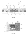
- Fig.10A is a partial enlarged view of a section of organic EL display panel 200 of Embodiment 2.
- the organic EL display panel of Embodiment 2 is identical to that of organic EL display panel 100 of Embodiment 1 except for the shape of the pixel-to-bus bank.
- the same components as those of organic EL display panel 100 are given the same references and descriptions thereof are not given.
- organic EL display panel 200 includes pixel-to-bus bank 207a and pixel-to-pixel bank 207b.
- Fig.10B is an enlarged view of the region surrounded by square X in Fig.10A .
- taper angle ⁇ of pixel-to-bus bank 207a is smaller than taper angle ⁇ of pixel-to-pixel bank 207b.
- Taper angle ⁇ of pixel-to-bus bank 207a is preferably 20° to 30°, and taper angle ⁇ of pixel-to-pixel bank 207b is preferably greater than 30° to 60°.
- the taper angle of pixel-to-bus bank 207a smaller than the taper angle of pixel-to-pixel bank 207b in this way, it is possible to level the edge height of an organic layer (hole transport layer and organic light-emitting layer) and thus to provide an organic layer with uniform thickness.
- the manufacturing method of organic EL display panel 200 is the same as that for organic EL display panel 100 except for the manufacturing method of banks. Thus, the following exclusively describes the manufacturing method of banks in the manufacturing method of organic EL display panel 200.
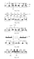
- Figs.11A to 11E are schematic illustrations of one example of a manufacturing method of organic EL display panel 200 of Embodiment 2.
- a manufacturing method of forming bank 207 of organic EL display panel 200 includes: 1) a first step of forming negative photosensitive resin film 106 on substrate 101 ( Fig.11A ); 2) a second step of exposing and developing photosensitive resin film 106 to pattern bank 207 ( Figs. 11B and 11C ); 3) a third step of re-exposing pixel-to-pixel bank 207b ( Fig.11D ); and 4 ) a forth step of baking bank 207 so as to be secured to substrate 101 ( Fig. 11E ).
- negative photosensitive resin film 106 is formed on substrate 101 on which bus electrode 105, pixel electrode 103, and hole injection layer 1111 are disposed. Formation of photosensitive resin film 106 on substrate 101 may be accomplished by applying a photosensitive resin composition over the substrate by spin coating, die coating, slit coating or the like and baking the formed film.
- photosensitive resin film 106 is exposed and developed to pattern bank 207.
- bank 207 By patterning bank 207, hole injection layer 111 and bus electrode 105 are exposed.
- pixel-to-pixel bank 207b is re-exposed. This step is performed between the second step and forth step. Exposure dose for re-exposure is, for example, 300 mJ/cm 2 . Re-exposure of pixel-to-pixel bank 207b results in elevation of glass transition temperature and elastic modulus.
- patterned bank 207 is baked. Because pixel-to-pixel bank 207b has a high glass transition temperature and a high elastic modulus as described above, the elastic modulus does not drop due to heat during the baking process, whereby, pixel-to-pixel bank 207b spreads toward the bottom to a lesser extent and thus has a large taper angle. On the other hand, since the glass transition temperature and elastic modulus of pixel-to-bus bank 207a, which is not re-exposed, remain low, the elastic modulus drops due to heat during the baking process. Thus, pixel-to-bus bank 207a spreads toward the bottom and thus has a small taper angle. In this way it is possible to make the taper angle of the pixel-to-bus bank smaller than the taper angle of the pixel-to-pixel bank.
- the conventional organic EL display panel has a problem that the edge height of an organic layer (hole transport layer and organic light-emitting layer) formed in a region defined by the pixel-to-bus bank and pixel-to-pixel bank becomes large on the pixel-to-bus bank side (see Fig.2E ).
- the taper angle of pixel-to-bus bank 207a smaller than the taper angle of pixel-to-pixel bank 207b as described above, it is possible to lower the edge height of the organic layer on the pixel-to-bus bank 207a side.
- Embodiment 2 by making the taper angle of the pixel-to-bus bank smaller than the taper angle of the pixel-to-pixel bank in this way, it is possible to level the edge height of an organic layer (hole transport layer and organic light-emitting layer) and thus to provide an organic layer with uniform thickness.
- the present invention enables to suppress organic layer thickness variation even when bus electrodes are provided, thus making it possible to provide an organic EL display panel that offers excellent luminous characteristics.
Landscapes
- Engineering & Computer Science (AREA)
- Microelectronics & Electronic Packaging (AREA)
- Physics & Mathematics (AREA)
- Optics & Photonics (AREA)
- Electroluminescent Light Sources (AREA)
Claims (8)
- Organisches EL-Display, das umfasst:ein Substrat (101);wenigstens zwei Pixel-Elektroden (103), die auf dem Substrat (101) angeordnet sind;eine Bus-Elektrode (105), die auf dem Substrat (101) angeordnet ist, wobei die Bus-Elektrode (105) an wenigstens eine der Pixel-Elektroden (103) angrenzend angeordnet ist;eine organische Schicht (109), die über den Pixel-Elektroden (103) angeordnet ist;wenigstens zwei Bänke (107), die auf dem Substrat (101) angeordnet sind, wobei die Bänke (107) einen Bereich bilden, in dem die organische Schicht (109) angeordnet ist; undeine Gegenelektrode (117), die über der organischen Schicht (109) angeordnet ist, wobei die Gegenelektrode (117) mit der Bus-Elektrode (105) verbunden ist,dadurch gekennzeichnet, dassdie wenigstens zwei Bänke (107) jeweils Fluor-Harz enthalten,die wenigstens zwei Bänke (107) eine Bank (107), die zwischen der Bus-Elektrode (105) und der angrenzenden Pixel-Elektrode (103) angeordnet ist, sowie eine Bank (107) enthalten, die zwischen den Pixel-Elektroden (103) angeordnet ist, undein lyophiler Charakter der Bank (107), die zwischen der Bus-Elektrode (105) und der angrenzenden Pixel-Elektrode (103) angeordnet ist, niedriger ist als ein lyophiler Charakter der Bank (107), die zwischen den Pixel-Elektroden (103) angeordnet ist.
- Organisches EL-Display nach Anspruch 1, wobei ein Anisol-Kontaktwinkel an einer oberen Fläche der zwischen den Pixel-Elektroden (103) angeordneten Bank (107) 30° bis 40° beträgt, und
ein Anisol-Kontaktwinkel an einer oberen Fläche der zwischen der Bus-Elektrode (105) und der angrenzenden Pixel-Elektrode (103) angeordneten Bank (107) 40° bis 55° beträgt. - Organisches EL-Display nach Anspruch 1, das des Weiteren eine Lochinjektions-Schicht (111) umfasst, die über der Pixel-Elektrode (103) angeordnet ist,
wobei die organische Schicht (109) eine Lochleitungs-Schicht (113), die auf der Lochinjektions-Schicht (111) angeordnet ist, und eine organische Lichtemissions-Schicht (115) enthält, die auf der Lochleitungs-Schicht (113) angeordnet ist. - Organisches EL-Display, das umfasst:ein Substrat (101);wenigstens zwei Pixel-Elektroden (103), die auf dem Substrat (101) angeordnet sind;eine Bus-Elektrode (105), die auf dem Substrat (101) angeordnet ist, wobei die Bus-Elektrode (105) an wenigstens eine der Pixel-Elektroden (103) angrenzend angeordnet ist;eine organische Schicht (109), die über den Pixel-Elektroden (103) angeordnet ist;wenigstens zwei Bänke (107), die auf dem Substrat (101) angeordnet sind, wobei die Bänke (107) einen Bereich bilden, in dem die organische Schicht (109) angeordnet ist; undeine Gegenelektrode (117), die über der organischen Schicht (109) angeordnet ist, wobei die Gegenelektrode (117) mit der Bus-Elektrode (105) verbunden ist,dadurch gekennzeichnet, dassdie wenigstens zwei Bänke (107) jeweils Fluor-Harz enthalten,die wenigstens zwei Bänke (107) eine Bank (107), die zwischen der Bus-Elektrode (105) und der angrenzenden Pixel-Elektrode (103) angeordnet ist, sowie eine Bank (107) enthalten, die zwischen den Pixel-Elektroden (103) angeordnet ist, undein Kegelwinkel der zwischen der Bus-Elektrode (105) und der angrenzenden Pixel-Elektrode (103) angeordneten Bank (107) kleiner ist als ein Kegelwinkel der zwischen den Pixel-Elektroden (103) angeordneten Bank (107).
- Organisches EL-Display nach Anspruch 4, wobei der Kegelwinkel der zwischen der Bus-Elektrode (105) und der angrenzenden Pixel-Elektrode (103) angeordneten Bank (107) zwischen 20° und 30° beträgt, und
der Kegelwinkel der zwischen den Pixel-Elektroden (103) angeordneten Bank (107) 30° bis 60° beträgt. - Organisches EL-Display nach Anspruch 4, das des Weiteren eine Lochinjektions-Schicht (111) umfasst, die über der Pixel-Elektrode (103) angeordnet ist,
wobei die organische Schicht (109) eine Lochleitungs-Schicht (113), die auf der Lochinjektions-Schicht (111) angeordnet ist, und eine organische Lichtemissions-Schicht (115) enthält, die auf der Lochleitungs-Schicht (113) angeordnet ist. - Verfahren zum Herstellen eines organischen EL-Displays nach Anspruch 1, das umfasst:Bereitstellen eines Substrats (101), das wenigstens zwei Pixel-Elektroden (103) und eine an wenigstens eine der Pixel-Elektroden (103) angrenzend angeordnete Bus-Elektrode (105) darauf aufweist;Ausbilden eines Films (106) aus fotoempfindlichem Harz auf dem Substrat (101);Belichten und Entwickeln des Films (106) aus fotoempfindlichem Harz, um wenigstens zwei Bänke (107) zu strukturieren, wobei die wenigstens zwei Bänke (107) eine Bank (107), die zwischen der Bus-Elektrode (105) und der angrenzenden Pixel-Elektrode (103) angeordnet ist, sowie eine Bank (107) enthalten, die zwischen den Pixel-Elektroden (103) angeordnet ist;Brennen der wenigstens zwei Bänke (107), um die wenigstens zwei Bänke (107) an dem Substrat (101) zu befestigen;Bestrahlen nur der zwischen den Pixel-Elektroden (103) angeordneten Bank (107) mit aktiven Strahlen; undAufbringen einer Tinte, die ein Material einer organischen Schicht (109) enthält, in einem Bereich, der sich über den Pixel-Elektroden (103) befindet und durch die wenigstens zwei Bänke (107) abgegrenzt wird, um eine organische Schicht (109) auszubilden.
- Verfahren zum Herstellen eines organischen EL-Displays nach Anspruch 4, das umfasst:Bereitstellen eines Substrats (101), das wenigstens zwei Pixel-Elektroden (103) und eine an wenigstens eine der Pixel-Elektroden (103) angrenzend angeordnete Bus-Elektrode (105) darauf aufweist;Ausbilden eines Films (106) aus negativem fotoempfindlichem Harz auf dem Substrat (101);Belichten und Entwickeln des Films (106) aus fotoempfindlichem Harz, um wenigstens zwei Bänke (107) zu strukturieren, wobei die wenigstens zwei Bänke (107) eine Bank (107), die zwischen der Bus-Elektrode (105) und der angrenzenden Pixel-Elektrode (103) angeordnet ist, sowie eine Bank (107), die zwischen den Pixel-Elektroden (103) angeordnet ist, enthalten;erneutes Belichten nur der zwischen den Pixel-Elektroden (103) angeordneten Bank (107);Brennen der wenigstens zwei Bänke (107), um die wenigstens zwei Bänke (107) an dem Substrat (101) zu befestigen; undAufbringen einer Tinte, die ein Material einer organischen Schicht (109) enthält, in einem Bereich, der sich über den Pixel-Elektroden (103) befindet und durch die wenigstens zwei Bänke (107) gebildet wird, um eine organische Schicht (109) auszubilden.
Applications Claiming Priority (2)
| Application Number | Priority Date | Filing Date | Title |
|---|---|---|---|
| JP2009135322 | 2009-06-04 | ||
| PCT/JP2010/003198 WO2010140301A1 (ja) | 2009-06-04 | 2010-05-11 | 有機elディスプレイパネルおよびその製造方法 |
Publications (3)
| Publication Number | Publication Date |
|---|---|
| EP2391187A1 EP2391187A1 (de) | 2011-11-30 |
| EP2391187A4 EP2391187A4 (de) | 2012-07-04 |
| EP2391187B1 true EP2391187B1 (de) | 2013-04-24 |
Family
ID=43297444
Family Applications (1)
| Application Number | Title | Priority Date | Filing Date |
|---|---|---|---|
| EP10783089.5A Active EP2391187B1 (de) | 2009-06-04 | 2010-05-11 | Organische el-anzeigetafel und verfahren zu ihrer herstellung |
Country Status (5)
| Country | Link |
|---|---|
| US (1) | US20110233572A1 (de) |
| EP (1) | EP2391187B1 (de) |
| JP (1) | JP4621818B1 (de) |
| CN (1) | CN102106186B (de) |
| WO (1) | WO2010140301A1 (de) |
Cited By (1)
| Publication number | Priority date | Publication date | Assignee | Title |
|---|---|---|---|---|
| WO2016198142A1 (en) | 2015-06-12 | 2016-12-15 | Merck Patent Gmbh | Organic electronic devices with fluoropolymer bank structures |
Families Citing this family (27)
| Publication number | Priority date | Publication date | Assignee | Title |
|---|---|---|---|---|
| JP3023645B2 (ja) | 1994-06-07 | 2000-03-21 | 新日本製鐵株式会社 | Pb含有鋼の連続鋳造方法 |
| JP3430642B2 (ja) | 1994-06-09 | 2003-07-28 | 大同特殊鋼株式会社 | 含カルシウム鋼の製造方法 |
| JP4951151B2 (ja) * | 2009-06-29 | 2012-06-13 | パナソニック株式会社 | 有機elディスプレイパネル |
| WO2012049713A1 (ja) * | 2010-10-15 | 2012-04-19 | パナソニック株式会社 | 有機発光パネルとその製造方法、および有機表示装置 |
| KR20130073012A (ko) * | 2010-10-15 | 2013-07-02 | 파나소닉 주식회사 | 유기 발광 패널과 그 제조 방법, 및 유기 표시 장치 |
| CN102577614B (zh) * | 2010-10-15 | 2015-11-25 | 株式会社日本有机雷特显示器 | 有机发光面板及其制造方法以及有机显示装置 |
| JPWO2013069274A1 (ja) * | 2011-11-10 | 2015-04-02 | パナソニック株式会社 | 有機表示パネル、有機表示装置、有機発光装置、それらの製造方法、および薄膜形成方法 |
| KR20140117206A (ko) * | 2013-03-26 | 2014-10-07 | 삼성디스플레이 주식회사 | 증착장치, 이를 이용한 유기발광 디스플레이 장치 제조 방법 및 유기발광 디스플레이 장치 |
| WO2015037237A1 (ja) | 2013-09-13 | 2015-03-19 | パナソニック株式会社 | 有機発光装置、およびその製造方法 |
| JP2015076220A (ja) * | 2013-10-08 | 2015-04-20 | セイコーエプソン株式会社 | 有機el素子の製造方法、有機el装置、及び電子機器 |
| WO2015178028A1 (ja) * | 2014-05-23 | 2015-11-26 | 株式会社Joled | 有機el表示パネル及び有機el表示装置 |
| KR102277380B1 (ko) * | 2015-01-12 | 2021-07-14 | 삼성디스플레이 주식회사 | 액정 표시 장치 및 그 제조 방법 |
| JP2017054723A (ja) * | 2015-09-10 | 2017-03-16 | 住友化学株式会社 | バンク付き基板 |
| CN106775039B (zh) * | 2015-11-20 | 2024-02-02 | 京东方科技集团股份有限公司 | 一种内嵌式触摸屏、其制作方法及显示装置 |
| JP2018142442A (ja) * | 2017-02-27 | 2018-09-13 | 株式会社ジャパンディスプレイ | 有機el表示装置の製造方法及び有機el表示装置 |
| CN109728031B (zh) * | 2017-10-31 | 2020-03-24 | 昆山国显光电有限公司 | 有机电致发光器件、显示器及移动通信设备 |
| CN107799575B (zh) * | 2017-10-31 | 2020-04-24 | 京东方科技集团股份有限公司 | 显示器基板、其制造方法、显示器及补偿构件贴片 |
| CN110165055B (zh) * | 2018-09-20 | 2021-12-21 | 合肥鑫晟光电科技有限公司 | 有机薄膜图案的制作方法及有机薄膜图案、阵列基板及显示装置 |
| KR102656492B1 (ko) * | 2018-12-31 | 2024-04-09 | 엘지디스플레이 주식회사 | 유기전계발광 표시장치 및 그 제조방법 |
| CN110491888A (zh) * | 2019-08-30 | 2019-11-22 | 京东方科技集团股份有限公司 | 显示面板、阵列基板及其制备方法 |
| CN111192905A (zh) * | 2020-01-08 | 2020-05-22 | 武汉华星光电半导体显示技术有限公司 | 有机发光二极体显示器件及其制造方法 |
| KR102837274B1 (ko) * | 2020-05-18 | 2025-07-22 | 삼성디스플레이 주식회사 | 디스플레이 장치 제조방법 |
| US11424270B2 (en) * | 2020-06-02 | 2022-08-23 | Wuhan China Star Optoelectronics Semiconductor Display Technology Co., Ltd. | Flexible display device and manufacturing method thereof |
| CN115474443B (zh) * | 2021-03-24 | 2026-03-31 | 京东方科技集团股份有限公司 | 显示面板及其制造方法、显示装置 |
| KR20230046350A (ko) * | 2021-09-29 | 2023-04-06 | 삼성디스플레이 주식회사 | 표시 장치 및 그 제조 방법 |
| KR20240032263A (ko) * | 2022-09-01 | 2024-03-12 | 삼성디스플레이 주식회사 | 표시 패널 |
| KR20240057518A (ko) * | 2022-10-24 | 2024-05-07 | 삼성디스플레이 주식회사 | 표시 패널 |
Family Cites Families (19)
| Publication number | Priority date | Publication date | Assignee | Title |
|---|---|---|---|---|
| WO2000067072A1 (en) | 1999-05-04 | 2000-11-09 | E.I. Du Pont De Nemours And Company | Fluorinated polymers, photoresists and processes for microlithography |
| JP2002318556A (ja) * | 2001-04-20 | 2002-10-31 | Toshiba Corp | アクティブマトリクス型平面表示装置およびその製造方法 |
| TWI257496B (en) * | 2001-04-20 | 2006-07-01 | Toshiba Corp | Display device and method of manufacturing the same |
| JP2003059660A (ja) * | 2001-08-17 | 2003-02-28 | Toshiba Corp | 自己発光型表示装置の製造方法 |
| AU2003260959A1 (en) * | 2002-09-11 | 2004-04-30 | Semiconductor Energy Laboratory Co., Ltd. | Light-emitting apparatus and fabrication method of the same |
| KR20040025383A (ko) | 2002-09-19 | 2004-03-24 | 삼성에스디아이 주식회사 | 유기 전계 발광 표시 장치 및 그 제조방법 |
| JP4290953B2 (ja) | 2002-09-26 | 2009-07-08 | 奇美電子股▲ふん▼有限公司 | 画像表示装置、有機el素子および画像表示装置の製造方法 |
| US7161184B2 (en) * | 2003-06-16 | 2007-01-09 | Semiconductor Energy Laboratory Co., Ltd. | Display device and method for manufacturing the same |
| JP4663257B2 (ja) | 2003-06-16 | 2011-04-06 | 株式会社半導体エネルギー研究所 | 発光装置及びその作製方法 |
| JP3951055B2 (ja) * | 2004-02-18 | 2007-08-01 | セイコーエプソン株式会社 | 有機エレクトロルミネッセンス装置及び電子機器 |
| JP2006113376A (ja) | 2004-10-15 | 2006-04-27 | Toshiba Matsushita Display Technology Co Ltd | 有機el表示装置及びアレイ基板 |
| JP2007080603A (ja) * | 2005-09-13 | 2007-03-29 | Seiko Epson Corp | 膜パターンの形成方法、デバイスの製造方法、有機エレクトロルミネッセンス装置 |
| JP2007103126A (ja) | 2005-10-03 | 2007-04-19 | Seiko Epson Corp | El表示装置、el表示装置の製造方法、電子機器 |
| JP2007115563A (ja) * | 2005-10-21 | 2007-05-10 | Seiko Epson Corp | 電気光学装置、電気光学装置の製造方法及び電子機器 |
| JP2007310156A (ja) * | 2006-05-18 | 2007-11-29 | Seiko Epson Corp | 膜形成方法、電気光学基板の製造方法、及び電気光学装置の製造方法、並びに機能膜、電気光学基板、電気光学装置、及び電子機器 |
| JP2008084541A (ja) * | 2006-09-25 | 2008-04-10 | Fujifilm Corp | 有機el表示装置及びその製造方法 |
| JP4967926B2 (ja) * | 2007-08-23 | 2012-07-04 | 大日本印刷株式会社 | 有機エレクトロルミネッセンス素子およびその製造方法 |
| JP2009135322A (ja) | 2007-11-30 | 2009-06-18 | Tdk Corp | 積層型電子部品の不良検出方法および積層型電子部品の製造方法 |
| JP4670875B2 (ja) * | 2008-02-13 | 2011-04-13 | セイコーエプソン株式会社 | 有機el装置 |
-
2010
- 2010-05-11 EP EP10783089.5A patent/EP2391187B1/de active Active
- 2010-05-11 WO PCT/JP2010/003198 patent/WO2010140301A1/ja not_active Ceased
- 2010-05-11 US US13/132,171 patent/US20110233572A1/en not_active Abandoned
- 2010-05-11 JP JP2010534308A patent/JP4621818B1/ja active Active
- 2010-05-11 CN CN201080002165.2A patent/CN102106186B/zh active Active
Cited By (1)
| Publication number | Priority date | Publication date | Assignee | Title |
|---|---|---|---|---|
| WO2016198142A1 (en) | 2015-06-12 | 2016-12-15 | Merck Patent Gmbh | Organic electronic devices with fluoropolymer bank structures |
Also Published As
| Publication number | Publication date |
|---|---|
| EP2391187A1 (de) | 2011-11-30 |
| US20110233572A1 (en) | 2011-09-29 |
| CN102106186A (zh) | 2011-06-22 |
| CN102106186B (zh) | 2014-04-09 |
| JP4621818B1 (ja) | 2011-01-26 |
| JPWO2010140301A1 (ja) | 2012-11-15 |
| EP2391187A4 (de) | 2012-07-04 |
| WO2010140301A1 (ja) | 2010-12-09 |
Similar Documents
| Publication | Publication Date | Title |
|---|---|---|
| EP2391187B1 (de) | Organische el-anzeigetafel und verfahren zu ihrer herstellung | |
| US7888867B2 (en) | Organic el device having bank with groove, organic el display panel, and method for manufacturing the organic el device | |
| US8901594B2 (en) | Organic EL display panel and method for manufacturing same | |
| JP5096648B1 (ja) | 有機elディスプレイパネル及びその製造方法 | |
| JP4974978B2 (ja) | 有機エレクトロルミネッセンス素子の製造方法 | |
| EP2221899B1 (de) | Organische el-anordnung, el-anzeigeschirm, verfahren zur herstellung der organischen el-anordnung und verfahren zur herstellung des el-anzeigeschirms | |
| US8304986B2 (en) | Organic EL display panel having specific inclination angle of wall surface | |
| KR100919353B1 (ko) | 유기 el 소자 및 그 제조 방법 | |
| US10861910B2 (en) | Organic EL display panel and method for manufacturing organic EL display panel | |
| US20150155516A1 (en) | Organic light-emitting element and production method therefor | |
| US8921838B2 (en) | Light emitting element, method for manufacturing same, and light emitting device | |
| KR101604155B1 (ko) | 발광 장치 및 그의 제조 방법 | |
| EP1688020B1 (de) | Anzeigetafel | |
| JP5092485B2 (ja) | 有機エレクトロルミネッセンスディスプレイ及びその製造方法 | |
| US20070019126A1 (en) | Display device and method of manufacturing the same | |
| CN109564984B (zh) | 具有岸结构的电子器件 |
Legal Events
| Date | Code | Title | Description |
|---|---|---|---|
| PUAI | Public reference made under article 153(3) epc to a published international application that has entered the european phase |
Free format text: ORIGINAL CODE: 0009012 |
|
| 17P | Request for examination filed |
Effective date: 20110520 |
|
| AK | Designated contracting states |
Kind code of ref document: A1 Designated state(s): AL AT BE BG CH CY CZ DE DK EE ES FI FR GB GR HR HU IE IS IT LI LT LU LV MC MK MT NL NO PL PT RO SE SI SK SM TR |
|
| A4 | Supplementary search report drawn up and despatched |
Effective date: 20120605 |
|
| RIC1 | Information provided on ipc code assigned before grant |
Ipc: H01L 27/32 20060101ALI20120530BHEP Ipc: H01L 51/50 20060101ALI20120530BHEP Ipc: H05B 33/10 20060101ALI20120530BHEP Ipc: H05B 33/12 20060101ALI20120530BHEP Ipc: H05B 33/22 20060101AFI20120530BHEP Ipc: H05B 33/26 20060101ALI20120530BHEP Ipc: H01L 51/52 20060101ALI20120530BHEP |
|
| DAX | Request for extension of the european patent (deleted) | ||
| GRAP | Despatch of communication of intention to grant a patent |
Free format text: ORIGINAL CODE: EPIDOSNIGR1 |
|
| GRAS | Grant fee paid |
Free format text: ORIGINAL CODE: EPIDOSNIGR3 |
|
| GRAA | (expected) grant |
Free format text: ORIGINAL CODE: 0009210 |
|
| AK | Designated contracting states |
Kind code of ref document: B1 Designated state(s): AL AT BE BG CH CY CZ DE DK EE ES FI FR GB GR HR HU IE IS IT LI LT LU LV MC MK MT NL NO PL PT RO SE SI SK SM TR |
|
| REG | Reference to a national code |
Ref country code: GB Ref legal event code: FG4D |
|
| REG | Reference to a national code |
Ref country code: CH Ref legal event code: EP |
|
| REG | Reference to a national code |
Ref country code: AT Ref legal event code: REF Ref document number: 609259 Country of ref document: AT Kind code of ref document: T Effective date: 20130515 |
|
| REG | Reference to a national code |
Ref country code: IE Ref legal event code: FG4D |
|
| REG | Reference to a national code |
Ref country code: DE Ref legal event code: R096 Ref document number: 602010006586 Country of ref document: DE Effective date: 20130627 |
|
| REG | Reference to a national code |
Ref country code: AT Ref legal event code: MK05 Ref document number: 609259 Country of ref document: AT Kind code of ref document: T Effective date: 20130424 |
|
| REG | Reference to a national code |
Ref country code: LT Ref legal event code: MG4D |
|
| REG | Reference to a national code |
Ref country code: NL Ref legal event code: VDEP Effective date: 20130424 |
|
| PG25 | Lapsed in a contracting state [announced via postgrant information from national office to epo] |
Ref country code: SE Free format text: LAPSE BECAUSE OF FAILURE TO SUBMIT A TRANSLATION OF THE DESCRIPTION OR TO PAY THE FEE WITHIN THE PRESCRIBED TIME-LIMIT Effective date: 20130424 Ref country code: ES Free format text: LAPSE BECAUSE OF FAILURE TO SUBMIT A TRANSLATION OF THE DESCRIPTION OR TO PAY THE FEE WITHIN THE PRESCRIBED TIME-LIMIT Effective date: 20130804 Ref country code: NO Free format text: LAPSE BECAUSE OF FAILURE TO SUBMIT A TRANSLATION OF THE DESCRIPTION OR TO PAY THE FEE WITHIN THE PRESCRIBED TIME-LIMIT Effective date: 20130724 Ref country code: LT Free format text: LAPSE BECAUSE OF FAILURE TO SUBMIT A TRANSLATION OF THE DESCRIPTION OR TO PAY THE FEE WITHIN THE PRESCRIBED TIME-LIMIT Effective date: 20130424 Ref country code: GR Free format text: LAPSE BECAUSE OF FAILURE TO SUBMIT A TRANSLATION OF THE DESCRIPTION OR TO PAY THE FEE WITHIN THE PRESCRIBED TIME-LIMIT Effective date: 20130725 Ref country code: BE Free format text: LAPSE BECAUSE OF FAILURE TO SUBMIT A TRANSLATION OF THE DESCRIPTION OR TO PAY THE FEE WITHIN THE PRESCRIBED TIME-LIMIT Effective date: 20130424 Ref country code: SI Free format text: LAPSE BECAUSE OF FAILURE TO SUBMIT A TRANSLATION OF THE DESCRIPTION OR TO PAY THE FEE WITHIN THE PRESCRIBED TIME-LIMIT Effective date: 20130424 Ref country code: FI Free format text: LAPSE BECAUSE OF FAILURE TO SUBMIT A TRANSLATION OF THE DESCRIPTION OR TO PAY THE FEE WITHIN THE PRESCRIBED TIME-LIMIT Effective date: 20130424 Ref country code: IS Free format text: LAPSE BECAUSE OF FAILURE TO SUBMIT A TRANSLATION OF THE DESCRIPTION OR TO PAY THE FEE WITHIN THE PRESCRIBED TIME-LIMIT Effective date: 20130824 Ref country code: AT Free format text: LAPSE BECAUSE OF FAILURE TO SUBMIT A TRANSLATION OF THE DESCRIPTION OR TO PAY THE FEE WITHIN THE PRESCRIBED TIME-LIMIT Effective date: 20130424 Ref country code: PT Free format text: LAPSE BECAUSE OF FAILURE TO SUBMIT A TRANSLATION OF THE DESCRIPTION OR TO PAY THE FEE WITHIN THE PRESCRIBED TIME-LIMIT Effective date: 20130826 |
|
| PG25 | Lapsed in a contracting state [announced via postgrant information from national office to epo] |
Ref country code: PL Free format text: LAPSE BECAUSE OF FAILURE TO SUBMIT A TRANSLATION OF THE DESCRIPTION OR TO PAY THE FEE WITHIN THE PRESCRIBED TIME-LIMIT Effective date: 20130424 Ref country code: BG Free format text: LAPSE BECAUSE OF FAILURE TO SUBMIT A TRANSLATION OF THE DESCRIPTION OR TO PAY THE FEE WITHIN THE PRESCRIBED TIME-LIMIT Effective date: 20130724 Ref country code: CY Free format text: LAPSE BECAUSE OF FAILURE TO SUBMIT A TRANSLATION OF THE DESCRIPTION OR TO PAY THE FEE WITHIN THE PRESCRIBED TIME-LIMIT Effective date: 20130424 Ref country code: LV Free format text: LAPSE BECAUSE OF FAILURE TO SUBMIT A TRANSLATION OF THE DESCRIPTION OR TO PAY THE FEE WITHIN THE PRESCRIBED TIME-LIMIT Effective date: 20130424 Ref country code: HR Free format text: LAPSE BECAUSE OF FAILURE TO SUBMIT A TRANSLATION OF THE DESCRIPTION OR TO PAY THE FEE WITHIN THE PRESCRIBED TIME-LIMIT Effective date: 20130424 |
|
| PG25 | Lapsed in a contracting state [announced via postgrant information from national office to epo] |
Ref country code: CZ Free format text: LAPSE BECAUSE OF FAILURE TO SUBMIT A TRANSLATION OF THE DESCRIPTION OR TO PAY THE FEE WITHIN THE PRESCRIBED TIME-LIMIT Effective date: 20130424 Ref country code: MC Free format text: LAPSE BECAUSE OF FAILURE TO SUBMIT A TRANSLATION OF THE DESCRIPTION OR TO PAY THE FEE WITHIN THE PRESCRIBED TIME-LIMIT Effective date: 20130424 Ref country code: SK Free format text: LAPSE BECAUSE OF FAILURE TO SUBMIT A TRANSLATION OF THE DESCRIPTION OR TO PAY THE FEE WITHIN THE PRESCRIBED TIME-LIMIT Effective date: 20130424 Ref country code: EE Free format text: LAPSE BECAUSE OF FAILURE TO SUBMIT A TRANSLATION OF THE DESCRIPTION OR TO PAY THE FEE WITHIN THE PRESCRIBED TIME-LIMIT Effective date: 20130424 Ref country code: DK Free format text: LAPSE BECAUSE OF FAILURE TO SUBMIT A TRANSLATION OF THE DESCRIPTION OR TO PAY THE FEE WITHIN THE PRESCRIBED TIME-LIMIT Effective date: 20130424 |
|
| REG | Reference to a national code |
Ref country code: IE Ref legal event code: MM4A |
|
| PG25 | Lapsed in a contracting state [announced via postgrant information from national office to epo] |
Ref country code: IT Free format text: LAPSE BECAUSE OF FAILURE TO SUBMIT A TRANSLATION OF THE DESCRIPTION OR TO PAY THE FEE WITHIN THE PRESCRIBED TIME-LIMIT Effective date: 20130424 Ref country code: NL Free format text: LAPSE BECAUSE OF FAILURE TO SUBMIT A TRANSLATION OF THE DESCRIPTION OR TO PAY THE FEE WITHIN THE PRESCRIBED TIME-LIMIT Effective date: 20130424 Ref country code: RO Free format text: LAPSE BECAUSE OF FAILURE TO SUBMIT A TRANSLATION OF THE DESCRIPTION OR TO PAY THE FEE WITHIN THE PRESCRIBED TIME-LIMIT Effective date: 20130424 |
|
| PLBE | No opposition filed within time limit |
Free format text: ORIGINAL CODE: 0009261 |
|
| STAA | Information on the status of an ep patent application or granted ep patent |
Free format text: STATUS: NO OPPOSITION FILED WITHIN TIME LIMIT |
|
| REG | Reference to a national code |
Ref country code: FR Ref legal event code: ST Effective date: 20140131 |
|
| 26N | No opposition filed |
Effective date: 20140127 |
|
| PG25 | Lapsed in a contracting state [announced via postgrant information from national office to epo] |
Ref country code: IE Free format text: LAPSE BECAUSE OF NON-PAYMENT OF DUE FEES Effective date: 20130511 |
|
| REG | Reference to a national code |
Ref country code: DE Ref legal event code: R097 Ref document number: 602010006586 Country of ref document: DE Effective date: 20140127 |
|
| PG25 | Lapsed in a contracting state [announced via postgrant information from national office to epo] |
Ref country code: FR Free format text: LAPSE BECAUSE OF NON-PAYMENT OF DUE FEES Effective date: 20130624 |
|
| REG | Reference to a national code |
Ref country code: CH Ref legal event code: PL |
|
| GBPC | Gb: european patent ceased through non-payment of renewal fee |
Effective date: 20140511 |
|
| PG25 | Lapsed in a contracting state [announced via postgrant information from national office to epo] |
Ref country code: CH Free format text: LAPSE BECAUSE OF NON-PAYMENT OF DUE FEES Effective date: 20140531 Ref country code: LI Free format text: LAPSE BECAUSE OF NON-PAYMENT OF DUE FEES Effective date: 20140531 |
|
| PG25 | Lapsed in a contracting state [announced via postgrant information from national office to epo] |
Ref country code: MT Free format text: LAPSE BECAUSE OF FAILURE TO SUBMIT A TRANSLATION OF THE DESCRIPTION OR TO PAY THE FEE WITHIN THE PRESCRIBED TIME-LIMIT Effective date: 20130424 |
|
| PG25 | Lapsed in a contracting state [announced via postgrant information from national office to epo] |
Ref country code: GB Free format text: LAPSE BECAUSE OF NON-PAYMENT OF DUE FEES Effective date: 20140511 Ref country code: SM Free format text: LAPSE BECAUSE OF FAILURE TO SUBMIT A TRANSLATION OF THE DESCRIPTION OR TO PAY THE FEE WITHIN THE PRESCRIBED TIME-LIMIT Effective date: 20130424 |
|
| PG25 | Lapsed in a contracting state [announced via postgrant information from national office to epo] |
Ref country code: TR Free format text: LAPSE BECAUSE OF FAILURE TO SUBMIT A TRANSLATION OF THE DESCRIPTION OR TO PAY THE FEE WITHIN THE PRESCRIBED TIME-LIMIT Effective date: 20130424 |
|
| PG25 | Lapsed in a contracting state [announced via postgrant information from national office to epo] |
Ref country code: LU Free format text: LAPSE BECAUSE OF NON-PAYMENT OF DUE FEES Effective date: 20130511 Ref country code: MK Free format text: LAPSE BECAUSE OF FAILURE TO SUBMIT A TRANSLATION OF THE DESCRIPTION OR TO PAY THE FEE WITHIN THE PRESCRIBED TIME-LIMIT Effective date: 20130424 Ref country code: HU Free format text: LAPSE BECAUSE OF FAILURE TO SUBMIT A TRANSLATION OF THE DESCRIPTION OR TO PAY THE FEE WITHIN THE PRESCRIBED TIME-LIMIT; INVALID AB INITIO Effective date: 20100511 |
|
| REG | Reference to a national code |
Ref country code: DE Ref legal event code: R082 Ref document number: 602010006586 Country of ref document: DE Representative=s name: GRUENECKER PATENT- UND RECHTSANWAELTE PARTG MB, DE Ref country code: DE Ref legal event code: R081 Ref document number: 602010006586 Country of ref document: DE Owner name: JOLED INC., TOKYO, JP Free format text: FORMER OWNER: PANASONIC CORPORATION, KADOMA-SHI, OSAKA, JP |
|
| PG25 | Lapsed in a contracting state [announced via postgrant information from national office to epo] |
Ref country code: AL Free format text: LAPSE BECAUSE OF FAILURE TO SUBMIT A TRANSLATION OF THE DESCRIPTION OR TO PAY THE FEE WITHIN THE PRESCRIBED TIME-LIMIT Effective date: 20130424 |
|
| REG | Reference to a national code |
Ref country code: DE Ref legal event code: R082 Ref document number: 602010006586 Country of ref document: DE Representative=s name: DENNEMEYER & ASSOCIATES S.A., DE Ref country code: DE Ref legal event code: R082 Ref document number: 602010006586 Country of ref document: DE Representative=s name: DENNEMEYER & ASSOCIATES RECHTSANWALTSGESELLSCH, DE Ref country code: DE Ref legal event code: R081 Ref document number: 602010006586 Country of ref document: DE Owner name: JDI DESIGN AND DEVELOPMENT G.K., JP Free format text: FORMER OWNER: JOLED INC., TOKYO, CHIYODA-KU, JP Ref country code: DE Ref legal event code: R081 Ref document number: 602010006586 Country of ref document: DE Owner name: MAGNOLIA BLUE CORPORATION, JP Free format text: FORMER OWNER: JOLED INC., TOKYO, CHIYODA-KU, JP Ref country code: DE Ref legal event code: R082 Ref document number: 602010006586 Country of ref document: DE Representative=s name: MERH-IP MATIAS ERNY REICHL HOFFMANN PATENTANWA, DE |
|
| REG | Reference to a national code |
Ref country code: DE Ref legal event code: R082 Ref document number: 602010006586 Country of ref document: DE Representative=s name: DENNEMEYER & ASSOCIATES RECHTSANWALTSGESELLSCH, DE Ref country code: DE Ref legal event code: R082 Ref document number: 602010006586 Country of ref document: DE Representative=s name: MERH-IP MATIAS ERNY REICHL HOFFMANN PATENTANWA, DE |
|
| PGFP | Annual fee paid to national office [announced via postgrant information from national office to epo] |
Ref country code: DE Payment date: 20250521 Year of fee payment: 16 |
|
| REG | Reference to a national code |
Ref country code: DE Ref legal event code: R081 Ref document number: 602010006586 Country of ref document: DE Owner name: MAGNOLIA BLUE CORPORATION, JP Free format text: FORMER OWNER: JDI DESIGN AND DEVELOPMENT G.K., TOKYO, JP Ref country code: DE Ref legal event code: R082 Ref document number: 602010006586 Country of ref document: DE Representative=s name: MERH-IP MATIAS ERNY REICHL HOFFMANN PATENTANWA, DE |