EP2390716B1 - LED-Rücklichtsystem für LCD-Anzeigen - Google Patents
LED-Rücklichtsystem für LCD-Anzeigen Download PDFInfo
- Publication number
- EP2390716B1 EP2390716B1 EP11175110.3A EP11175110A EP2390716B1 EP 2390716 B1 EP2390716 B1 EP 2390716B1 EP 11175110 A EP11175110 A EP 11175110A EP 2390716 B1 EP2390716 B1 EP 2390716B1
- Authority
- EP
- European Patent Office
- Prior art keywords
- light
- waveguide
- leds
- liquid crystal
- crystal display
- Prior art date
- Legal status (The legal status is an assumption and is not a legal conclusion. Google has not performed a legal analysis and makes no representation as to the accuracy of the status listed.)
- Ceased
Links
- 239000004973 liquid crystal related substance Substances 0.000 claims description 26
- 230000002093 peripheral effect Effects 0.000 claims description 5
- 238000004891 communication Methods 0.000 claims description 3
- 238000005286 illumination Methods 0.000 description 10
- 239000000463 material Substances 0.000 description 9
- 238000009792 diffusion process Methods 0.000 description 6
- 238000007493 shaping process Methods 0.000 description 5
- 230000008878 coupling Effects 0.000 description 4
- 238000010168 coupling process Methods 0.000 description 4
- 238000005859 coupling reaction Methods 0.000 description 4
- 238000004519 manufacturing process Methods 0.000 description 4
- 238000005259 measurement Methods 0.000 description 4
- 238000000034 method Methods 0.000 description 4
- 230000003287 optical effect Effects 0.000 description 4
- 239000000758 substrate Substances 0.000 description 4
- 230000005540 biological transmission Effects 0.000 description 3
- 230000000694 effects Effects 0.000 description 3
- 238000005516 engineering process Methods 0.000 description 3
- 239000011521 glass Substances 0.000 description 3
- 238000013021 overheating Methods 0.000 description 3
- PXHVJJICTQNCMI-UHFFFAOYSA-N Nickel Chemical compound [Ni] PXHVJJICTQNCMI-UHFFFAOYSA-N 0.000 description 2
- 229920003023 plastic Polymers 0.000 description 2
- 239000010453 quartz Substances 0.000 description 2
- 238000004064 recycling Methods 0.000 description 2
- VYPSYNLAJGMNEJ-UHFFFAOYSA-N silicon dioxide Inorganic materials O=[Si]=O VYPSYNLAJGMNEJ-UHFFFAOYSA-N 0.000 description 2
- RYGMFSIKBFXOCR-UHFFFAOYSA-N Copper Chemical compound [Cu] RYGMFSIKBFXOCR-UHFFFAOYSA-N 0.000 description 1
- VVQNEPGJFQJSBK-UHFFFAOYSA-N Methyl methacrylate Chemical compound COC(=O)C(C)=C VVQNEPGJFQJSBK-UHFFFAOYSA-N 0.000 description 1
- 229920005372 Plexiglas® Polymers 0.000 description 1
- 239000000654 additive Substances 0.000 description 1
- 230000000996 additive effect Effects 0.000 description 1
- 230000004888 barrier function Effects 0.000 description 1
- 239000002131 composite material Substances 0.000 description 1
- 229910052802 copper Inorganic materials 0.000 description 1
- 239000010949 copper Substances 0.000 description 1
- 230000001419 dependent effect Effects 0.000 description 1
- 230000001627 detrimental effect Effects 0.000 description 1
- 239000008393 encapsulating agent Substances 0.000 description 1
- 239000011888 foil Substances 0.000 description 1
- PCHJSUWPFVWCPO-UHFFFAOYSA-N gold Chemical compound [Au] PCHJSUWPFVWCPO-UHFFFAOYSA-N 0.000 description 1
- 239000010931 gold Substances 0.000 description 1
- 229910052737 gold Inorganic materials 0.000 description 1
- 238000007654 immersion Methods 0.000 description 1
- 238000007373 indentation Methods 0.000 description 1
- 229910052751 metal Inorganic materials 0.000 description 1
- 239000002184 metal Substances 0.000 description 1
- 150000002739 metals Chemical class 0.000 description 1
- 238000012986 modification Methods 0.000 description 1
- 230000004048 modification Effects 0.000 description 1
- 229910052759 nickel Inorganic materials 0.000 description 1
- 238000007747 plating Methods 0.000 description 1
- 238000012552 review Methods 0.000 description 1
- 239000007787 solid Substances 0.000 description 1
- 238000011144 upstream manufacturing Methods 0.000 description 1
Images


Classifications
-
- G—PHYSICS
- G02—OPTICS
- G02F—OPTICAL DEVICES OR ARRANGEMENTS FOR THE CONTROL OF LIGHT BY MODIFICATION OF THE OPTICAL PROPERTIES OF THE MEDIA OF THE ELEMENTS INVOLVED THEREIN; NON-LINEAR OPTICS; FREQUENCY-CHANGING OF LIGHT; OPTICAL LOGIC ELEMENTS; OPTICAL ANALOGUE/DIGITAL CONVERTERS
- G02F1/00—Devices or arrangements for the control of the intensity, colour, phase, polarisation or direction of light arriving from an independent light source, e.g. switching, gating or modulating; Non-linear optics
- G02F1/01—Devices or arrangements for the control of the intensity, colour, phase, polarisation or direction of light arriving from an independent light source, e.g. switching, gating or modulating; Non-linear optics for the control of the intensity, phase, polarisation or colour
- G02F1/13—Devices or arrangements for the control of the intensity, colour, phase, polarisation or direction of light arriving from an independent light source, e.g. switching, gating or modulating; Non-linear optics for the control of the intensity, phase, polarisation or colour based on liquid crystals, e.g. single liquid crystal display cells
- G02F1/133—Constructional arrangements; Operation of liquid crystal cells; Circuit arrangements
- G02F1/1333—Constructional arrangements; Manufacturing methods
- G02F1/1335—Structural association of cells with optical devices, e.g. polarisers or reflectors
- G02F1/1336—Illuminating devices
- G02F1/133615—Edge-illuminating devices, i.e. illuminating from the side
-
- G—PHYSICS
- G02—OPTICS
- G02B—OPTICAL ELEMENTS, SYSTEMS OR APPARATUS
- G02B6/00—Light guides; Structural details of arrangements comprising light guides and other optical elements, e.g. couplings
- G02B6/0001—Light guides; Structural details of arrangements comprising light guides and other optical elements, e.g. couplings specially adapted for lighting devices or systems
- G02B6/0011—Light guides; Structural details of arrangements comprising light guides and other optical elements, e.g. couplings specially adapted for lighting devices or systems the light guides being planar or of plate-like form
- G02B6/0075—Arrangements of multiple light guides
- G02B6/0076—Stacked arrangements of multiple light guides of the same or different cross-sectional area
-
- G—PHYSICS
- G02—OPTICS
- G02F—OPTICAL DEVICES OR ARRANGEMENTS FOR THE CONTROL OF LIGHT BY MODIFICATION OF THE OPTICAL PROPERTIES OF THE MEDIA OF THE ELEMENTS INVOLVED THEREIN; NON-LINEAR OPTICS; FREQUENCY-CHANGING OF LIGHT; OPTICAL LOGIC ELEMENTS; OPTICAL ANALOGUE/DIGITAL CONVERTERS
- G02F1/00—Devices or arrangements for the control of the intensity, colour, phase, polarisation or direction of light arriving from an independent light source, e.g. switching, gating or modulating; Non-linear optics
- G02F1/01—Devices or arrangements for the control of the intensity, colour, phase, polarisation or direction of light arriving from an independent light source, e.g. switching, gating or modulating; Non-linear optics for the control of the intensity, phase, polarisation or colour
- G02F1/13—Devices or arrangements for the control of the intensity, colour, phase, polarisation or direction of light arriving from an independent light source, e.g. switching, gating or modulating; Non-linear optics for the control of the intensity, phase, polarisation or colour based on liquid crystals, e.g. single liquid crystal display cells
- G02F1/133—Constructional arrangements; Operation of liquid crystal cells; Circuit arrangements
- G02F1/1333—Constructional arrangements; Manufacturing methods
- G02F1/1335—Structural association of cells with optical devices, e.g. polarisers or reflectors
- G02F1/133524—Light-guides, e.g. fibre-optic bundles, louvered or jalousie light-guides
-
- G—PHYSICS
- G02—OPTICS
- G02F—OPTICAL DEVICES OR ARRANGEMENTS FOR THE CONTROL OF LIGHT BY MODIFICATION OF THE OPTICAL PROPERTIES OF THE MEDIA OF THE ELEMENTS INVOLVED THEREIN; NON-LINEAR OPTICS; FREQUENCY-CHANGING OF LIGHT; OPTICAL LOGIC ELEMENTS; OPTICAL ANALOGUE/DIGITAL CONVERTERS
- G02F1/00—Devices or arrangements for the control of the intensity, colour, phase, polarisation or direction of light arriving from an independent light source, e.g. switching, gating or modulating; Non-linear optics
- G02F1/01—Devices or arrangements for the control of the intensity, colour, phase, polarisation or direction of light arriving from an independent light source, e.g. switching, gating or modulating; Non-linear optics for the control of the intensity, phase, polarisation or colour
- G02F1/13—Devices or arrangements for the control of the intensity, colour, phase, polarisation or direction of light arriving from an independent light source, e.g. switching, gating or modulating; Non-linear optics for the control of the intensity, phase, polarisation or colour based on liquid crystals, e.g. single liquid crystal display cells
- G02F1/133—Constructional arrangements; Operation of liquid crystal cells; Circuit arrangements
- G02F1/1333—Constructional arrangements; Manufacturing methods
- G02F1/1335—Structural association of cells with optical devices, e.g. polarisers or reflectors
- G02F1/1336—Illuminating devices
- G02F1/133602—Direct backlight
- G02F1/133603—Direct backlight with LEDs
-
- G—PHYSICS
- G02—OPTICS
- G02B—OPTICAL ELEMENTS, SYSTEMS OR APPARATUS
- G02B6/00—Light guides; Structural details of arrangements comprising light guides and other optical elements, e.g. couplings
- G02B6/0001—Light guides; Structural details of arrangements comprising light guides and other optical elements, e.g. couplings specially adapted for lighting devices or systems
- G02B6/0011—Light guides; Structural details of arrangements comprising light guides and other optical elements, e.g. couplings specially adapted for lighting devices or systems the light guides being planar or of plate-like form
- G02B6/0013—Means for improving the coupling-in of light from the light source into the light guide
- G02B6/0023—Means for improving the coupling-in of light from the light source into the light guide provided by one optical element, or plurality thereof, placed between the light guide and the light source, or around the light source
- G02B6/0028—Light guide, e.g. taper
-
- G—PHYSICS
- G02—OPTICS
- G02B—OPTICAL ELEMENTS, SYSTEMS OR APPARATUS
- G02B6/00—Light guides; Structural details of arrangements comprising light guides and other optical elements, e.g. couplings
- G02B6/0001—Light guides; Structural details of arrangements comprising light guides and other optical elements, e.g. couplings specially adapted for lighting devices or systems
- G02B6/0011—Light guides; Structural details of arrangements comprising light guides and other optical elements, e.g. couplings specially adapted for lighting devices or systems the light guides being planar or of plate-like form
- G02B6/0033—Means for improving the coupling-out of light from the light guide
- G02B6/0035—Means for improving the coupling-out of light from the light guide provided on the surface of the light guide or in the bulk of it
- G02B6/0038—Linear indentations or grooves, e.g. arc-shaped grooves or meandering grooves, extending over the full length or width of the light guide
-
- G—PHYSICS
- G02—OPTICS
- G02B—OPTICAL ELEMENTS, SYSTEMS OR APPARATUS
- G02B6/00—Light guides; Structural details of arrangements comprising light guides and other optical elements, e.g. couplings
- G02B6/0001—Light guides; Structural details of arrangements comprising light guides and other optical elements, e.g. couplings specially adapted for lighting devices or systems
- G02B6/0011—Light guides; Structural details of arrangements comprising light guides and other optical elements, e.g. couplings specially adapted for lighting devices or systems the light guides being planar or of plate-like form
- G02B6/0066—Light guides; Structural details of arrangements comprising light guides and other optical elements, e.g. couplings specially adapted for lighting devices or systems the light guides being planar or of plate-like form characterised by the light source being coupled to the light guide
- G02B6/0068—Arrangements of plural sources, e.g. multi-colour light sources
Definitions
- the invention relates generally to liquid crystal displays and, more specifically, to liquid crystal displays having enhanced lighting uniformity.
- CTR cathode ray tube
- LCDs liquid crystal displays
- plasma displays These newer display technologies offer various advantages over traditional CRT technology, including reduced weight; thinner profile; superior color, contrast and brightness in the resulting display; and reduced power consumption.
- LCDs typically include an array of pixels arranged in front of a light source, lighting panel, or reflector. Each pixel includes a layer of liquid crystal material, and two filters, with one filter serving to polarize light horizontally and the other filter serving to polarize light vertically.
- a reflective LCD has a reflective layer (such as a mirror) behind the pixels and is lit by either a frontlight or by ambient light.
- a transmissive LCD is lit by a backlight, in an arrangement where the pixels are arranged in front of a light source and light from the light source is transmitted through the pixels to the front of the LCD or the viewing area, resulting in a "lit" pixel.
- Light sources for backlighting may include electroluminescent panels/foils (ELs), cold cathode fluorescent lamps (CCFLs), hot cathode fluorescent lamps (HCFLs) External Electrode Fluorescent Lamps (EEFLs), traditional incandescent light bulbs, or light emitting diodes (LEDs). High intensity discharge lamps (HIDs) may also be used in certain backlighting applications.
- ELs electroluminescent panels/foils
- CCFLs cold cathode fluorescent lamps
- HCFLs hot cathode fluorescent lamps
- EFLs External Electrode Fluorescent Lamps
- LEDs light emitting diodes
- High intensity discharge lamps (HIDs) may also be used in certain backlighting applications.
- LEDs When LEDs are utilized as light sources for transmissive LCD backlighting, they may be traditional or side view LEDs. Side view LEDs are also known as “side emitting LEDs" or “side looker LEDs.” A side view LED is a packaged LED that emits light parallel to the plane of the surface to which the package is mounted. Compared to traditional LED packages, side view LED packages are thinner and typically less expensive to manufacture. A typical side view LED package has dimensions of about 1.5 mm by about 0.5-0.7 mm, but such dimensions may vary. Owing at least in part to their small size, side view LED packages have limited current handling capabilities, thus limiting their emissions. As a result, a single side view LED package typically has less output capability than a traditional LED package. Whether accidentally or deliberately, practitioners often "overcurrent" side view LEDs to achieve greater output, which can lead to overheating and failure of a device incorporating such LEDs.
- transmissive LCDs include either direct backlighting or backlighting by edge illumination. While a backlight will light the pixels from the backside, that light may come from directly behind the center of the pixels (direct backlighting) or from behind the sides of the pixels (backlighting by edge illumination). While both techniques are recognized as backlighting, direct backlighting refers to illumination directed axially (centrally) through the backside of pixels. In contrast, edge illumination refers to an arrangement where the light source is located along an edge of a LCD system and lights the pixels from the side. Edge illumination may occur along the side edges of the LCD, the top edge, or the bottom edge. Backlighting of transmissive LCDs may utilize a waveguide to spread the light to an entire LCD panel, with such waveguide having a single entry for light and transmitting the light by internal reflection to be spread over a desired area.
- a traditionally LED backlit LCD may include a layered system that includes an array of red, green and blue LEDs positioned on a panel or array of tiles.
- the panel or tiles include a reflective surface or layer arranged so that light is reflected in the desired direction toward aa diffusion layer that diffuses the light provided from the LED backlight and reflects some of the light back toward the reflective surface or layer, thereby functioning to mix the light and improve the light uniformity ("recycling effect").
- a brightness enhancement film and/or collimating layer over the reflective layer or surface and the diffusion layer provides light to the LCD panel layers in a more optimal fashion and also acts with the reflective layer or surface and the diffusion layer to enhance the recycling effect Depending on the embodiment, additional or less layers can be utilized as is understood by one of skill in the art.
- Such a backlight system may also include thermal layers below the LEDs for thermal management. As such, as is understood by one of skill in the art, the LED backlight system provides uniform white light to the LCD panels, which typically include a shutter layer and red, green and blue color
- a traditional LED package emits light directly at (i.e., through) a LCD screen.
- the LED In order to light the entire screen, the LED must operate at high power and be very thick if utilized without a waveguide. Accordingly, the thickness of the resulting LCD system (television, monitor, etc.) is also increased.
- Modern consumers desire thinner profile systems with thicknesses as small as a few inches. Accordingly, thick LCD systems are not commercially desirable.
- use of high powered traditional LED package without a waveguide may create a "headlight effect" also known as a "hot spot" on the panel, causing a detrimental lack of light uniformity.
- edge illumination in which a waveguide is used to spread the light emission of a side view LED package disposed on an edge of the LCD, the resulting screen size is limited.
- light emission characteristics of side view LED packages are reduced in comparison to traditional LED packages, with such limitation due to their size and current handling capabilities.
- one or more portions ( i.e. , typically the center) of a side view LED-lighted LCD screen may not be lit if the screen is relatively large in size.
- LCD screens illuminated with side view LED packages and having acceptably uniform illumination characteristics are currently limited to screens of about 30 to 36 cm (12 to 14 inches) (diagonal) in size.
- U.S. Patent Publication No. 2006/022935 A1 discloses edge backlighting of multiple light guide plates using LEDs arranged along edges of the guide plates (e.g., guide plates 135-138 in FIG. 30) or edge backlighting of multiple light guide plates using LEDs arranged behind the light guide plates aided by side reflectors.
- International Publication No. WO 01/84046 A1 discloses edge illumination using LEDs arranged along edges of light-transmitting panels, wherein panel sub-surfaces remotely located from the light sources project light in a forward direction.
- European Patent No. 1 775 623 A1 discloses an image display apparatus utilizing multiple edge-lit waveguides for providing different display images to multiple observers.
- U.S. Patent Publication No. 2005/259939 A1 discloses an ultra-thin lighting element including one or more edge-lit light guide layers with multiple discrete fine optic surface relief structures.
- U.S. Patent Publication No. 2006/002146 A1 discloses a backlight unit and LCD display device using one or more light guide plates defining centrally arranged groove-type recesses therein to receive one or more light guide plates defining centrally arranged groove-type recesses therein to receive side-emitting LEDs to emit light laterally into the light guide plates.
- 2006/083019 A1 discloses a backlight apparatus for use with a LCD in which multiple bar-shaped LED light sources are arranged on a reflective plate to laterally emit light to be received by a single transparent plate, with the light sources covered by light shades to prevent direct backlighting, and with the single transparent plate including secondary light sources.
- U.S. Patent Publication No. 2005/169012 A1 discloses a liquid crystal display utilizing a centrally placed electroluminescent device in combination with multiple LEDs placed along edges of a transparent substrate.
- Japanese Publication No. JP 2003-222864 A discloses a backlight for a LCD display utilizing multiple fluorescent tubes arranged behind a light guide plate and multiple LED tubes arranged proximate to two side faces of the light guide plate.
- U.S. Patent Publication No. 2007/063943 A1 discloses an edge-lit display panel that displays individual images in multiple viewing directions on a common screen, including a parallax barrier that makes individual images respectively visible from multiple directions.
- the present invention provides an improved liquid crystal display systems according to claim 1, as further delimited by the dependent claims.
- a liquid crystal display (LCD) system comprising a LCD panel, at least one waveguide element comprising a plurality of light entry regions, a first light-emitting source positioned to emit light into the at least one waveguide element at a first light entry region of the plurality of light entry regions, and at least a second light-emitting source positioned to emit light into the at least one waveguide element at at least a second light entry region of the plurality of light entry regions.
- LCD liquid crystal display
- a liquid crystal display (LCD) system comprises a LCD panel with a viewable surface having a diagonal measurement of at least about 30 cm (12 inches), at least one waveguide element comprising a plurality of light entry regions, a first light-emitting source positioned to emit light into the at least one waveguide element at a first light entry region of the plurality of light entry regions, and at least a second light-emitting source positioned to emit light into the at least one waveguide element at least a second light entry region of the plurality of light entry regions; wherein each of the first light-emitting source and the at least second light-emitting source comprises a plurality of LEDs arranged in at least one strip.
- liquid crystal display (LCD) system comprising a LCD panel, at least one waveguide element comprising at least one light entry region, a first light-emitting source positioned to emit light into the at least one waveguide element at a light entry region, and at least a second light-emitting source positioned to emit direct backlight onto the LCD panel.
- LCD liquid crystal display
- a waveguide system comprising a first waveguide element comprising at least one light entry region; a first light-emitting source positioned to emit light into the first waveguide element at the first light entry region; at least a second waveguide element comprising at least one light entry region; and at least a second light-emitting source positioned to emit light into the at least a second waveguide element at the first light entry region.
- LCD systems utilizing waveguide systems.
- a LCD system comprises a LCD panel or screen, at least one waveguide with multiple entry regions for light, and at least two light-emitting sources positioned to emit light into the at least one waveguide.
- the waveguide transmits light sufficient to light the entire LCD panel or screen of the system.
- multiple waveguides may be employed, each with at least one entry region for light and at least one associated light-emitting source positioned to emit light into the waveguides. With multiple waveguides, each waveguide may be positioned to light a portion of the LCD panel.
- a conventional LCD system generally includes a LCD panel and a light source such as a LED optionally coupled to a single waveguide element having a single light entry point.
- a light source such as a LED optionally coupled to a single waveguide element having a single light entry point.
- Side view LED packages are desirable for use in LCD systems, due to their low current usage and small size. Due to concerns of overheating, however, the current that can be supplied to side view LED packages is limited, thus limiting their emissions. Consequently, the amount of light that can be emitted from a single side view LED package into a conventional waveguide is also limited. Therefore, side view LED packages coupled to single-input waveguides are not well-suited for use in backlighting LCD panels having viewable diagonal measurements larger than approximately 30 to 36 cm (12-14 inches).
- LCD systems embodied in the present invention may include, but are not limited to televisions and computer monitors.
- single waveguides having multiple light entry regions for receiving light from locations other than, and/or in addition to, a single edge of the waveguide.
- the provision of light into at least one waveguide from multiple entry regions permits low current side view LED packages, whether alone or with other types of light sources, to uniformly light a LCD panel or screen, even if the LCD panel or screen has a viewable surface with a diagonal measurement greater than approximately 30 to 36 cm (12-14 inches).
- waveguide systems comprising multiple waveguides each waveguide having at least a single light entry region.
- Such a waveguide system may be utilized in a LCD system, where each waveguide has a transmissive surface that lights a portion of the LCD panel.
- the provision of light to multiple waveguides permits use of low current side view LED packages, whether alone or with other types of light sources, to uniformly light the LCD panel.
- a LCD system as disclosed herein may include any suitable type of conventional LCD panel or screen.
- a LCD panel includes LCD pixels arranged in front of a light source or reflective surface to illuminate the pixels.
- the LCD may include an LCD shutter panel and/or color filters, such as RGB color filters, as are known to those of skill in the art.
- a LCD system disclosed herein may include a transmissive LCD, such that the light is provided to the LCD panel or screen from behind via at least one waveguide element.
- the at least one waveguide element disperses the light in an even and complete manner, such that the entire panel is lit consistently and at a consistent intensity.
- a single waveguide element may be utilized.
- multiple waveguide elements may be utilized with a single LCD panel.
- a waveguide element is a device utilized to guide optical waves from a light entry region to a transmissive surface or exit region of the waveguide element.
- a waveguide element may comprise a hollow structure with a reflective internal surface; alternatively, a waveguide may be substantially solid in nature.
- the waveguide element may also be surrounded in whole or in part by a material such as plastic to reflect any light back into the element.
- the waveguide includes a prism. At least a portion of a waveguide may be substantially planar or tubular in shape, or of any other configuration known to those of skill in the art.
- Total internal reflection is desirable, such that all of the light supplied to the waveguide element from associated light source(s) is transmitted out of the waveguide element via the transmissive surface. Internal reflection guides the optical waves to a transmissive surface of the waveguide element, which is optically coupled to provide light to the LCD screen or panel, such that the LCD panel or screen may be lit by the transmitted light.
- a waveguide is generally utilized in an arrangement where the LCD panel or screen is located between the waveguide element and a viewer.
- the waveguide When a single waveguide element is used, the waveguide preferably has multiple light entry regions. Additionally, the transmissive surface of the waveguide element and the viewable surface of the LCD panel or screen are preferably of substantially the same size. Optionally, the waveguide may contain gaps or holes to allow light from a direct backlight to the LCD panel or screen.
- Waveguides utilized in LCD systems disclosed herein may be utilized in combination, and when multiple waveguides are employed in a waveguide system, each may have one or more light entry regions. Light enters the one or more light entry regions of a waveguide and is transmitted to the transmissive surface thereof.
- a transmissive surface is preferably substantially flat to conform to a LCD panel. This transmissive surface provides backlight to the LCD panel, and is capable of lighting the viewable surface of the LCD panel or screen.
- multiple waveguides may be utilized in lighting the LCD panel or screen.
- each waveguide preferably has at least one light entry region.
- the combined transmissive surface area of the waveguide elements is preferably substantially the same as that of the viewable surface area of the LCD panel or screen.
- Each waveguide of the group may light a different portion of the LCD panel, or the combined transmission may light substantially all of the LCD panel.
- the waveguides may be spaced sufficiently to allow light from a direct backlight to the LCD screen or panel or any of the individual waveguides of the group may contain gaps or holes to allow light from a direct backlight to the LCD panel or screen.
- multiple waveguides When multiple waveguides are employed, they may abut one another laterally, or at least portions thereof may be disposed in a front-to-back or layered relationship if desired.
- multiple upstream waveguides may be optically coupled to a downstream waveguide to promote easy fabrication and/or enhance uniformity of light distribution.
- a light entry region of a waveguide element as disclosed herein may be adapted to receive light from one or more light sources.
- Light entry regions may be arranged along any convenient portion of a waveguide element. If a front portion of a waveguide is optically coupled to transmit light to a LCD panel or screen, then light entry regions may be disposed along any of a top edge, a first side edge, a second side edge, a bottom edge, and a back side of the waveguide element.
- a waveguide element as disclosed herein may be also adapted for use with a direct backlight source.
- a traditionally backlit LCD system includes a layered system which may include a direct backlight and, optionally, thermal layers under the light source, reflective layer(s), diffusion layer(s), brightness enhancement film(s) and/or collimating layer(s).
- a waveguide element disclosed herein is adapted for use with a direct backlight source, such that the waveguide element is included within or in addition to the layered backlight system.
- direct backlighting is provided in a LCD system disclosed herein, inclusion and orientation of such layers, films and elements, including one or more waveguide elements, is provided to optimize the direct backlight transmitted to the LCD panel or screen.
- a waveguide element may be provided between the direct backlight source and the diffusion layer.
- a waveguide element may serve as a diffusion layer.
- Multiple waveguides may form a "waveguide system" such that in one implementation, light transmitted from each of the waveguides is coupled to provide light to the LCD panel or screen of a LCD system.
- a waveguide system as disclosed herein may include two or more waveguides arranged in a layered configuration, where each waveguide provides light to a different portion of a LCD panel, such that the entire panel is substantially illuminated by the waveguide system.
- Each individual waveguide within the waveguide system includes one or more light entry regions, to which one or more light sources are optically coupled.
- Each waveguide also includes a transmissive surface or an exit region, where light exits the waveguide.
- a transmissive surface may comprise glass, quartz, or other optically transmissive materials, and maybe referred to as a "prismatic" section of the waveguide. Portions of the waveguide not comprising a transmissive surface may comprise materials without prismatic or transmissive properties.
- the waveguide may also comprise a material or be surface treated such that a light shined directly at the waveguide will enter the waveguide or pass through the waveguide.
- layered waveguides may be alternated with layers of diffusers and/or "light shaping" components.
- FIG. 6A illustrates a LCD screen 42 lit by a two layer waveguide system according to one implementation.
- a first waveguide (not shown) is arranged to provide lighting to a central portion 45 of the LCD screen 42 and a second waveguide (not shown) is arranged to provide lighting to a peripheral or outer section 46 of the LCD screen 42 .
- Each waveguide of the waveguide system preferably receives light from at least one different light source (not shown).
- FIG. 6B provides a cross-sectional view of an exemplary waveguide system 41 used to light a LCD screen 42 such as illustrated in FIG. 6A , taken along section lines B-B of FIG. 6A .
- the waveguide layers 44A, 44B may be of similar size to one another.
- the waveguides 44A, 44B are positioned in a layered configuration, such that one waveguide 44A is positioned between the second waveguide 44B and the LCD screen 42 .
- Each waveguide 44A, 44B has a transmissive or prismatic portion 49A, 49B on a major surface that emits light toward the LCD screen 42 .
- Each waveguide 44A, 44B lights a portion of the LCD screen 42 , such that the LCD screen 42 is substantially lit.
- a waveguide system may optionally be backed by a mirror or white light diffuser 40 , and/or may contain additional diffusers or light shaping components (not shown) between the waveguide layers 44A, 44B .
- a waveguide system includes three layered waveguides, with a first waveguide lighting a central or interior region of the LCD screen, a second waveguide lighting a first portion of a peripheral or exterior region of the LCD screen, and a third waveguide lighting a second (e.g., remaining) portion of the peripheral or exterior region of the LCD screen.
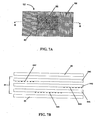
- FIG. 7A illustrates an exemplary lit LCD screen 52 utilizing a three layer waveguide system 51 .
- a first waveguide (not shown) is arranged to provide lighting to a first portion 55 along the center of the LCD screen 52
- a second waveguide (not shown) is arranged to provide lighting to a second portion 56 along the exterior of the LCD screen 52
- a third waveguide (not shown) is arranged to provide lighting to a third portion 57 along a remaining exterior portion of the LCD screen 52 .
- Each waveguide 54A-54C of the waveguide system preferably receives light from at least one different light source (not shown).
- FIG. 7B provides a cross-sectional view of an exemplary waveguide system 51 used to light LCD screen 52 as illustrated in FIG. 7A , taken along section lines B-B of FIG. 7A . As can be seen in FIG.
- each waveguide layer 54A-54C of the exemplary three waveguide system 51 may be of similar size.
- the waveguides 54A-54C are positioned in a layered configuration, such that one waveguide 54A is positioned closest to the LCD screen 52 and the third waveguide 54C is positioned furthest from the LCD screen 52 , with the second waveguide 54B positioned between the first and third waveguides 54A, 54C .
- Each waveguide 54A-54C has a transmissive or prismatic portion 59A-59C on a major surface thereof that emits light toward the LCD screen 52 .
- Each waveguide 54A-54C lights a portion of the LCD screen 52 , such that the entire LCD screen 52 is substantially lit.
- the waveguide system 51 may optionally be backed by a mirror or white light diffuser 50 , and/or may contain additional diffusers or light shaping components (not shown) between the waveguide layers 54A-54C .
- the waveguides may each provide light to a different portion (e.g., quadrants) of a LCD screen.
- FIG. 8A illustrates such an exemplary LCD screen 62 lit by a four layer waveguide system.
- a first waveguide (not shown) is arranged to provide lighting to a first portion 65 corresponding to an upper left quadrant of the LCD screen 62
- a second waveguide (not shown) is arranged to provide lighting to a second portion 66 corresponding to a lower left quadrant of the LCD screen 62
- a third waveguide (not shown) is arranged to provide lighting to a third portion 67 corresponding to an upper right quadrant of the LCD screen 62
- a fourth waveguide (not shown) is arranged to provide lighting to a fourth portion 68 corresponding to a lower right quadrant of the LCD screen 62 .
- Each waveguide of the waveguide system preferably receives light from at least one different light source (not shown).
- FIG. 8B provides a first cross-sectional view of a waveguide system 61 useable to light the LCD screen 62 of FIG. 8A , taken along section lines B-B of FIG. 8A .
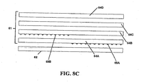
- FIG. 8C provides an alternative cross-sectional view of a first waveguide system useable to light the LCD screen 62 of FIG. 8A , taken along section lines C-C.
- the waveguide layers 64A-64D are of similar size to one another.
- the waveguides 64A-64D are positioned in a layered configuration, such that a first waveguide 64A is positioned closest to the LCD screen 62 and a fourth waveguide 64D is positioned furthest from the LCD screen 62 , with a second waveguide 64B and a third waveguide 64C positioned between the first and fourth waveguides 64A, 64D .
- Each waveguide 64A-64D has a transmissive or prismatic portion 69A-69D on its surface that emits light toward the LCD screen 62 .
- Each waveguide 64A-64D lights a portion of the LCD screen 62 , such that the entire LCD screen 62 is substantially lit.
- the waveguide system 61 is optionally backed by a mirror or white light diffuser (not shown) and may contain additional diffusers or light shaping components (not shown) between the waveguide layers 64A-64D.
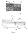
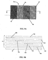
- FIG. 9A illustrates an exemplary LCD screen 72 lit by another four layer waveguide system.
- a first waveguide lights a first portion 75 of the LCD screen 72
- a second waveguide lights a second portion 76 of the LCD screen 72
- a third waveguide lights a third portion 77 of the LCD screen 72
- a fourth waveguide lights a fourth portion 78 of the LCD screen 72 .
- Each waveguide 74A-74D of the waveguide system preferably receives light from at least one different light source (not shown).
- FIG. 9B provides a cross-sectional view of a waveguide system 71 useable to light the LCD screen 72 of FIG. 9A , taken along section lines B-B of FIG. 9A . As can be seen in FIG.
- the waveguide layers 74A-74D are of similar size to one another.
- the waveguides 74A-74D are positioned in a layered configuration, such that a first waveguide 74A is positioned closest to the LCD screen 72 and a fourth waveguide 74D is positioned furthest from the LCD screen 72 , with a second waveguide 74B and a third waveguide 74C positioned between the first and fourth waveguides 74A , 74D .
- Each waveguide 74A-74D has a transmissive or prismatic portion 79A-79D on its surface that emits light toward the LCD screen 72 .
- Each waveguide 74A-74D lights a portion of the LCD screen 72 , such that the entire LCD screen 72 is substantially lit.
- the waveguide system 71 is optionally backed by a mirror or white light diffuser (not shown) and may contain additional diffusers or light shaping components (not shown) between the waveguide layers 74A-74D .
- the exemplary waveguide systems described above are not limited to the particular transmission configurations provided herein. Any number of waveguides may be arranged in any configuration such that the transmissive sections of the waveguides illuminate various sections of a LCD screen. Transmission by the waveguides in any particular configuration does not have to be evenly distributed among individual waveguides.
- the exemplary waveguide systems set forth above include waveguides of approximately similar size; however, the waveguides of a waveguide system may be of any size, as long as the resulting transmissive sections of those waveguides illuminate substantially all of the LCD screen.
- one or more light sources are optically coupled to a waveguide element in various implementations. Any number of light sources may be employed to achieve uniform lighting of a LCD panel. While the light sources are optically coupled to emit light into the light entry regions of the waveguide element, the number of light entry regions does not limit the number of light sources.
- at least one waveguide element is utilized, including a first light-emitting source positioned to emit light into a first entry region of the at least one waveguide element and a second light-emitting source positioned to emit light into a second entry region of the at least one waveguide element. Additional light-emitting sources and light entry regions may be employed.
- a light-emitting source may be positioned anywhere within a LCD system that allows optical coupling of the light emitted into a light entry region. Accordingly, light-emitting sources may be located in or along a side region, a top region, a bottom region and/or a rear region of the LCD system. Light-emitting sources may be spaced apart from corresponding light entry regions, may be adjacent to corresponding light entry regions, and/or may be physically coupled to the corresponding light entry regions. In one implementation, the light-emitting sources include side view LED packages, the light-emitting sources are arranged to not simultaneously and solely emit light into a top edge and a bottom edge of the waveguide.
- light sources may be arranged in locations other than both the top and bottom edges of the waveguide, or light sources arranged along both the top and bottom edge of a waveguide are supplemented with at least one additional light source arranged to emit light into the waveguide from at least one other location.
- Optical coupling between a light source and waveguide element may include any of: directing light to one or more recesses defined a waveguide element, embedding a light source in a waveguide element, and directing light to at least one edge or surface of a waveguide element.
- the waveguide element does not need to be uniform in shape and, optionally, may contain one or more extensions oriented in any suitable direction, such that the light source may be optically coupled to the waveguide element via the one or more extensions.
- waveguide extensions may be optionally oriented in a manner such that they are angled, bent, or curved toward a primary plane of the waveguide element itself and, correspondingly, toward the LCD panel, to achieve a thinner profile system.
- a LCD system may further comprise a light source that is not optically coupled to emit light into the waveguide.
- An exemplary system includes a light source that directly backlights a LCD panel, supplemented by waveguide-directed light. Light emitted by such a backlight may pass through or around a waveguide or waveguide system disposed between the backlight and the LCD panel, in order to transmit light from the backlight to the LCD panel.
- the backlight provides light to the LCD panel or screen, which light is supplemented in one or more locations by light transmitted by the waveguide or waveguide system.
- a LCD system may further comprise a direct backlight source that is optically coupled into the waveguide as understood by one of skill in the art.
- An exemplary system includes a light source that provides light optically coupled into the waveguide, where the light source is positioned directly behind the LCD panel.
- Such direct backlighting may be coupled into the waveguide by any means known to those of skill in the art.
- the LED is provided at the end of a waveguide extension.
- Such a waveguide extension may be oriented in any manner as more fully described above. Preferably such an extension is short and the backlight is flush with the extension.
- the waveguide comprises such a material or is surface-treated such that a direct backlight shined on the waveguide will enter the waveguide through the surface and will be optically coupled to light provided to the waveguide through additional light entry sources.
- the waveguide contains a light entry source in the form of a notch, or groove or other indentation in the surface of the waveguide, allowing for placement of a direct backlight directly against the waveguide. Light emitted from the direct backlight can therefore be optically coupled directly into the waveguide.
- Light sources useful in lighting a LCD panel can include any of: a cold cathode fluorescent lamp (CCFL), a hot cathode fluorescent lamp (HCFL), an electroluminescent panel (ELP), an incandescent light bulb, a light emitting diode (LED), an organic light emitting diode (OLED), a high intensity discharge (HID) lamp, and any combination of the foregoing sources arranged to provide light in additive or spatially discrete arrangement.
- CCFL cold cathode fluorescent lamp
- HCFL hot cathode fluorescent lamp
- ELP electroluminescent panel
- LED light emitting diode
- OLED organic light emitting diode
- HID high intensity discharge
- LEDs are utilized as light sources in systems disclosed herein, such LEDs are preferably embodied in LED packages.
- Such packages may include packaged traditional LEDs that emit light from a side opposite the electrode from which they receive current, and/or may be packaged side view LEDs (also known as “side emitting LEDs” or “sidelooker LEDs”) that emit light substantially parallel to a plane of the surface on which the package is mounted.
- a "LED package,” as used herein, preferably includes a substrate, an electrode, a LED chip mounted on or over the substrate and an encapsulant disposed on or over the LED chip.
- a LED package may also include any of: a diffuser, a reflector, a lens, an electrostatic discharge diode, and/or thermal conduction elements.
- a light source in a LCD system disclosed herein may include a LED that emits any of white light, blue light, red light, green light, or light of any desirable wavelength.
- a light source includes one or more clusters of red-green-blue (RGB) LEDs. Such clusters may be independently controlled.
- a light source includes a blue LED coated or otherwise covered with phosphors to upconvert blue light to white light.
- Exemplary combinations of light sources disclosed herein include: (1) direct backlighting utilizing one or more side view LEDs, supplemented with edge backlighting utilizing one or more side view LEDs; (2) direct backlighting utilizing one or more traditional LEDs, supplemented with edge backlighting utilizing one or more side view LEDs; (3) direct backlighting utilizing one or more side view LEDs, supplemented with edge backlighting utilizing one or more traditional LEDs; (4) direct backlighting utilizing one or more traditional LEDs, supplemented with edge backlighting utilizing one or more traditional LEDs; and (5) edge backlighting from more than one edge, utilizing one or more side view LEDs or traditional LEDs, or any combinations thereof.
- Such combinations may include, but are not limited to, single light sources including both traditional and side view LEDs.
- the foregoing combinations represent mere examples of possible configurations; other configurations may be employed with devices disclosed herein.
- a single light source may comprise a plurality of LEDs.
- the LEDs of such a plurality of LEDs may be arranged in any suitable configuration, whether to enable convenient manufacture, to maximize light emitted into the light entry regions of the at least one waveguide element, or both.
- Exemplary arrangements include multiple LED packages arranged in a strip, or a single LED package containing multiple LEDs arranged in a strip.
- Such a strip may contain two or more LEDs or LED packages.
- Individual LEDs or LED packages within a single strip maybe characteristically the same as, or different from, other LEDs or LED packages in the same strip.
- LEDs or LED packages in a single strip may be adapted to emit substantially the same wavelength, or may be adapted to emit different wavelengths.
- multiple strips may be connected to one another in any suitable orientation, such as in an end-to-end orientation, or in a side-to-side orientation, in order to yield a single composite light source to emit light into the waveguide element. Where multiple strips are utilized, each strip may be adapted to emit light of substantially the same wavelength as other strips, or may be adapted to emit light of wavelengths different from light other strips.
- a light source including a strip of LEDs or LED packages may include a circuit board or other common structural support, such that the LEDs may be electrically connected to one another.
- the LEDs may be further electrically connected to components adapted to provide uniform performance of the plurality of LEDs.
- Such components may include one or more common control circuits (e.g., integrated circuits or processors) to regulate, for example, power to the LEDs, intensity of the emitted light, wavelength of the emitted light, and/or other parameters.
- a strip of LEDs may include or be connected to one or more common electrostatic discharge (ESD) diodes, providing protection from voltage spikes to multiple LEDs within the strip.
- ESD electrostatic discharge
- FIG. 5 illustrates of an exemplary light source for use in a LCD system, including a plurality of LED packages arranged in a strip 100 .
- the strip 100 has dimensions of 20 mm x 2.5 mm and contains five or more LED packages 101A-101E, which maybe disposed in series.
- a strip 100 comprises a circuit board 105 including a 2.5 mil thickness FR4 substrate and 1 oz. copper, electroless Nickel Immersion Gold plating, and does not contain soldermask on the back surface.
- the strip 100 includes a common ESD diode 102 in electrical communication with the LEDs 101A-101E .
- Contacts 103, 104 may be provided to serve as common electrical inputs for the strip 100.
- a single light source comprises a plurality of LED packages
- any desirable number of LED packages may be provided. Factors affecting the makeup of a single light source may include: the size of the panel being lit, the desired viewing angle, the entry angle of the light into the light entry region of the waveguide element, the spacing of the individual LED packages, the brightness of the individual LED packages, and the size of the LED packages.
- plural light sources coupled to at least one waveguide utilized in a system as described herein are adapted to uniformly light a LCD panel of any desired size.
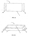
- FIG. 1A is a schematic front view illustration of at least a portion of an exemplary LCD system 1 including a LCD panel 2 and multiple light sources 3A, 3B .
- FIG. 1B is a schematic side view illustration of the system of FIG. 1A , depicting the LCD panel 2 , light sources 3A, 3B and waveguide element 4 .
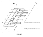
- FIG. 1C is a schematic side view illustration of an exemplary light source 3B , comprising a plurality of side view LED packages, 6A - 6E arranged as a strip on base 7 and emitting light 8 , parallel to the plane of base 7 , into waveguide 4 .
- FIG. 2 is a schematic perspective view illustration of at least a portion of an exemplary LCD system 11 , including a LCD panel 12 , waveguide element 14 , first light source 13 , and additional light sources 15A-15D , each coupled to the waveguide element 14 at the end of waveguide extensions 16A-16D , respectively.
- the first light source 13 provides light to a light entry region located along a lateral edge of the waveguide element 14 and additional strips of LED packages 15A-15D are optically coupled to the waveguide element 14 along light entry regions on extensions 16A-16D of the waveguide element 14 .
- FIG. 3 is a schematic perspective view illustration of at least a portion of an exemplary LCD system 21 , the system including a LCD panel 22 , waveguide element 24 , and light sources 23, 25A, 25B coupled to the waveguide element 24 along an edge 27 of a primary waveguide surface and at the ends of waveguide extensions 26A, 26B , respectively. Additional light sources (not shown) are contemplated to be coupled to the waveguide element 24 at the end of waveguide extensions 26C and 26D , and along edge 28 .
- Waveguide extensions 26A-26D are curved toward a primary plane of the waveguide element 24 , such that the side profile of the resulting system 21 is thinner than it would otherwise be if the extensions 26A-26D were straight.
- FIG. 4 is a schematic perspective view illustration view of an exemplary LCD system 31 .
- the system 31 includes a LCD panel 32 , a waveguide element 34 , a first light source 33 optically coupled to an edge 37 of the waveguide element 34 , and additional light sources 34A-34I optically coupled to the back side 35 of the waveguide element 34 .
- a LED panel may be lit by any combination of light sources that provides complete and uniform illumination of the panel.
- Light may be provided to the panel from light sources located along edge or back regions of the waveguide element, by direct backlighting, or use of any combination of light sources arranged to emit light directly to a LED panel and/or to emit light into one or more interposing waveguide elements.
Landscapes
- Physics & Mathematics (AREA)
- Nonlinear Science (AREA)
- General Physics & Mathematics (AREA)
- Optics & Photonics (AREA)
- Mathematical Physics (AREA)
- Chemical & Material Sciences (AREA)
- Crystallography & Structural Chemistry (AREA)
- Planar Illumination Modules (AREA)
- Liquid Crystal (AREA)
- Light Guides In General And Applications Therefor (AREA)
- Led Device Packages (AREA)
Claims (11)
- Flüssigkristallanzeige- (LCD-) System, Folgendes umfassend:a) ein Flüssigkristallanzeigefeld, einen Sichtbereich umfassend;b) einen ersten Wellenleiter, mindestens einen ersten Lichteingangsbereich umfassend, und einen zweiten Wellenleiter, mindestens einen zweiten Lichteingangsbereich umfassend;c) eine erste lichtemittierende Quelle, eine erste Mehrzahl an lichtemittierenden Dioden (LEDs) umfassend, wobei die erste Mehrzahl an LEDs entlang mindestens einer Kante des ersten Wellenleiters angeordnet und so positioniert ist, dass sie an dem mindestens einen ersten Lichteingangsbereich Licht in den ersten Wellenleiter emittiert; sowied) eine zweite lichtemittierende Quelle, eine zweite Mehrzahl an LEDs umfassend, die innerhalb des Sichtbereichs positioniert und direkt hinter den Pixeln des Flüssigkristallanzeigefelds angeordnet ist, um Licht in den mindestens einen zweiten Lichteingangsbereich zu emittieren, um direktes Gegenlicht auf das Flüssigkristallanzeigefeld zu emittieren;wobei die erste lichtemittierende Quelle und die zweite lichtemittierende Quelle so angeordnet sind, dass sie unterschiedliche Abschnitte des Flüssigkristallanzeigefeldes beleuchten.
- Flüssigkristallanzeigesystem nach Anspruch 1, wobei der zweite Wellenleiter so angeordnet ist, dass er einen zentralen Abschnitt des Flüssigkristallanzeigefeldes beleuchtet, und der erste Wellenleiter so angeordnet ist, dass er einen peripheren Abschnitt des Flüssigkristallanzeigefeldes beleuchtet.
- Flüssigkristallanzeigesystem nach Anspruch 1, wobei der erste Wellenleiter und der zweite Wellenleiter in einer geschichteten Konfiguration angeordnet sind.
- Flüssigkristallanzeigesystem nach Anspruch 1, wobei der erste Wellenleiter und der zweite Wellenleiter seitlich aneinander angrenzen.
- Flüssigkristallanzeigesystem nach Anspruch 1, wobei der mindestens eine erste Lichteingangsbereich mehrere, aus Folgenden ausgewählte Lichteingangsbereiche umfasst: eine Oberkante des ersten Wellenleiters, eine Unterkante des ersten Wellenleiters, eine erste Seitenkante des ersten Wellenleiters und eine zweite Seitenkante des ersten Wellenleiters.
- Flüssigkristallanzeigesystem nach Anspruch 1, wobei die zweite lichtemittierende Quelle innerhalb einer Fläche des zweiten Wellenleiters eingebettet oder in mindestens einer Vertiefung angeordnet ist, die auf einer Fläche des zweiten Wellenleiters definiert ist.
- Flüssigkristallanzeigesystem nach Anspruch 1, wobei die erste Mehrzahl an LEDs in mindestens einem ersten Streifen (100) und die zweite Mehrzahl an LEDs in mindestens einem zweiten Streifen (100) angeordnet ist.
- Flüssigkristallanzeigesystem nach Anspruch 7, wobei jeder des mindestens einen ersten Streifens (100) und des mindestens einen zweiten Streifens (100) eine elektrostatische Entladungsdiode (102) umfasst, die in elektrischer Verbindung mit der Mehrzahl an LEDs (101A-101E) steht, die im zugehörigen mindestens einen Streifen (100) angeordnet ist.
- Flüssigkristallanzeigesystem nach Anspruch 1, wobei sowohl die erste Mehrzahl an LEDs (101A-101E) als auch die zweite Mehrzahl an LEDs (101A-101E) LEDs umfasst, die geeignet sind, sich voneinander unterscheidende Wellenlängen zu emittieren.
- Flüssigkristallanzeigesystem nach einem der Ansprüche 1 bis 9, ferner eine gemeinsame Regelschaltung umfassend, die mit der ersten lichtemittierenden Quelle und der zweiten lichtemittierenden Quelle in elektrischer Verbindung steht.
- Flüssigkristallanzeigesystem nach einem der Ansprüche 1 bis 9, wobei mindestens einige LEDs der zweiten Mehrzahl an LEDs LEDs umfassen, die so angeordnet sind, dass sie Weißlichtemissionen ausgeben.
Applications Claiming Priority (2)
| Application Number | Priority Date | Filing Date | Title |
|---|---|---|---|
| US11/829,912 US7872705B2 (en) | 2007-07-29 | 2007-07-29 | LED backlight system for LCD displays |
| EP08159050A EP2023193A1 (de) | 2007-07-29 | 2008-06-25 | LED-Rückbeleuchtungssystem für LCD-Anzeigen |
Related Parent Applications (2)
| Application Number | Title | Priority Date | Filing Date |
|---|---|---|---|
| EP08159050.7 Division | 2008-06-25 | ||
| EP08159050A Division EP2023193A1 (de) | 2007-07-29 | 2008-06-25 | LED-Rückbeleuchtungssystem für LCD-Anzeigen |
Publications (3)
| Publication Number | Publication Date |
|---|---|
| EP2390716A2 EP2390716A2 (de) | 2011-11-30 |
| EP2390716A3 EP2390716A3 (de) | 2012-12-19 |
| EP2390716B1 true EP2390716B1 (de) | 2015-08-12 |
Family
ID=39720585
Family Applications (3)
| Application Number | Title | Priority Date | Filing Date |
|---|---|---|---|
| EP11175110.3A Ceased EP2390716B1 (de) | 2007-07-29 | 2008-06-25 | LED-Rücklichtsystem für LCD-Anzeigen |
| EP11175104.6A Ceased EP2390715B1 (de) | 2007-07-29 | 2008-06-25 | LED-Rücklichtsystem für LCD-Anzeigen |
| EP08159050A Ceased EP2023193A1 (de) | 2007-07-29 | 2008-06-25 | LED-Rückbeleuchtungssystem für LCD-Anzeigen |
Family Applications After (2)
| Application Number | Title | Priority Date | Filing Date |
|---|---|---|---|
| EP11175104.6A Ceased EP2390715B1 (de) | 2007-07-29 | 2008-06-25 | LED-Rücklichtsystem für LCD-Anzeigen |
| EP08159050A Ceased EP2023193A1 (de) | 2007-07-29 | 2008-06-25 | LED-Rückbeleuchtungssystem für LCD-Anzeigen |
Country Status (3)
| Country | Link |
|---|---|
| US (5) | US7872705B2 (de) |
| EP (3) | EP2390716B1 (de) |
| JP (2) | JP5178372B2 (de) |
Families Citing this family (69)
| Publication number | Priority date | Publication date | Assignee | Title |
|---|---|---|---|---|
| US8128272B2 (en) | 2005-06-07 | 2012-03-06 | Oree, Inc. | Illumination apparatus |
| US8215815B2 (en) * | 2005-06-07 | 2012-07-10 | Oree, Inc. | Illumination apparatus and methods of forming the same |
| US8272758B2 (en) | 2005-06-07 | 2012-09-25 | Oree, Inc. | Illumination apparatus and methods of forming the same |
| US20090001397A1 (en) * | 2007-05-29 | 2009-01-01 | Oree, Advanced Illumiation Solutions Inc. | Method and device for providing circumferential illumination |
| US7872705B2 (en) * | 2007-07-29 | 2011-01-18 | Cree, Inc. | LED backlight system for LCD displays |
| US8104911B2 (en) | 2007-09-28 | 2012-01-31 | Apple Inc. | Display system with distributed LED backlight |
| US8182128B2 (en) * | 2007-12-19 | 2012-05-22 | Oree, Inc. | Planar white illumination apparatus |
| US7907804B2 (en) * | 2007-12-19 | 2011-03-15 | Oree, Inc. | Elimination of stitch artifacts in a planar illumination area |
| CN101978297A (zh) * | 2008-03-05 | 2011-02-16 | 奥利高级照明解决公司 | 照明装置及其形成方法 |
| JP2010021131A (ja) * | 2008-06-09 | 2010-01-28 | Hitachi Ltd | 表示装置及びそれに用いられるバックライトユニット |
| US8297786B2 (en) | 2008-07-10 | 2012-10-30 | Oree, Inc. | Slim waveguide coupling apparatus and method |
| US8301002B2 (en) * | 2008-07-10 | 2012-10-30 | Oree, Inc. | Slim waveguide coupling apparatus and method |
| CN102177710B (zh) * | 2008-10-09 | 2013-10-30 | Tp视觉控股有限公司 | 显示设备、控制显示设备的发光二极管阵列的方法 |
| US20100098377A1 (en) * | 2008-10-16 | 2010-04-22 | Noam Meir | Light confinement using diffusers |
| WO2010082479A1 (ja) * | 2009-01-19 | 2010-07-22 | パナソニック株式会社 | 画像表示装置および画像表示方法 |
| US20100208470A1 (en) * | 2009-02-10 | 2010-08-19 | Yosi Shani | Overlapping illumination surfaces with reduced linear artifacts |
| JP5143770B2 (ja) * | 2009-03-02 | 2013-02-13 | 株式会社ジャパンディスプレイイースト | 液晶表示装置 |
| US8624527B1 (en) | 2009-03-27 | 2014-01-07 | Oree, Inc. | Independently controllable illumination device |
| US8328406B2 (en) * | 2009-05-13 | 2012-12-11 | Oree, Inc. | Low-profile illumination device |
| WO2010150202A2 (en) | 2009-06-24 | 2010-12-29 | Oree, Advanced Illumination Solutions Inc. | Illumination apparatus with high conversion efficiency and methods of forming the same |
| US8319764B2 (en) * | 2009-06-29 | 2012-11-27 | Research In Motion Limited | Wave guide for improving light sensor angular response |
| JP5628918B2 (ja) * | 2009-08-27 | 2014-11-19 | エルジー エレクトロニクス インコーポレイティド | バックライトユニット及びディスプレイ装置 |
| DE102010001266B4 (de) * | 2010-01-27 | 2025-08-07 | Zumtobel Lighting Gmbh | Anordnung zur Lichtabgabe |
| US8403539B2 (en) * | 2010-02-26 | 2013-03-26 | Research In Motion Limited | Light guide for improving device lighting |
| JP5440304B2 (ja) * | 2010-03-19 | 2014-03-12 | 富士通株式会社 | 光半導体装置及びその製造方法 |
| SG182817A1 (en) * | 2010-03-24 | 2012-09-27 | Nitto Denko Corp | A method and structure for coupling light from a light source into a planar waveguide |
| KR101767452B1 (ko) * | 2010-07-05 | 2017-08-14 | 삼성디스플레이 주식회사 | 액정 표시 장치의 백라이트 유닛 |
| EP4249964B1 (de) * | 2010-07-07 | 2025-10-15 | DEKA Products Limited Partnership | Medizinisches behandlungssystem und verfahren anhand der verwendung mehrerer flüssigkeitsleitungen |
| US9071676B2 (en) * | 2011-02-03 | 2015-06-30 | Bayer Healthcare Llc | Component illumination apparatus, systems, and electronic devices and methods of manufacturing and using same |
| JP2012226967A (ja) * | 2011-04-19 | 2012-11-15 | Sharp Corp | 照明装置、及びそれを備えた照明機器 |
| US9164247B2 (en) * | 2011-07-28 | 2015-10-20 | Source Photonics, Inc. | Apparatuses for reducing the sensitivity of an optical signal to polarization and methods of making and using the same |
| US9081125B2 (en) | 2011-08-08 | 2015-07-14 | Quarkstar Llc | Illumination devices including multiple light emitting elements |
| US8591072B2 (en) | 2011-11-16 | 2013-11-26 | Oree, Inc. | Illumination apparatus confining light by total internal reflection and methods of forming the same |
| CN103133939B (zh) * | 2011-11-30 | 2015-02-04 | 展晶科技(深圳)有限公司 | 背光模块的光源结构 |
| US10030846B2 (en) * | 2012-02-14 | 2018-07-24 | Svv Technology Innovations, Inc. | Face-lit waveguide illumination systems |
| US9857519B2 (en) | 2012-07-03 | 2018-01-02 | Oree Advanced Illumination Solutions Ltd. | Planar remote phosphor illumination apparatus |
| EP2895794B1 (de) | 2012-09-13 | 2018-06-27 | Quarkstar LLC | Beleuchtungssysteme für direkte und indirekte beleuchtung |
| US12117639B2 (en) * | 2013-03-12 | 2024-10-15 | Azumo, Inc. | Film-based lightguide with interior light directing edges with curved sections in a tapered light mixing region |
| US20150015142A1 (en) * | 2013-07-11 | 2015-01-15 | Huizhou Light Engine Limited | Led light bulb with leds mounted on angled circuit board |
| EP3081846B1 (de) | 2013-07-18 | 2018-03-28 | Quarkstar LLC | Beleuchtungsvorrichtung mit nicht zur optischen achse der vorrichtung paralleler quellenlichteinspeisung |
| CN110553165A (zh) | 2013-09-17 | 2019-12-10 | 夸克星有限责任公司 | 用于直接-间接照明的光导照明装置 |
| US11655950B2 (en) * | 2014-03-15 | 2023-05-23 | Ideal Industries Lighting Llc | Lighting devices having optical waveguides for controlled light distribution |
| WO2015178300A1 (ja) * | 2014-05-23 | 2015-11-26 | シャープ株式会社 | 照明装置、及び表示装置 |
| US9966000B2 (en) * | 2015-01-16 | 2018-05-08 | Apple Inc. | Electro-static discharge and electric overstress protection strategy for micro-chip array on panel |
| CN104914623A (zh) * | 2015-06-19 | 2015-09-16 | 深圳市华星光电技术有限公司 | 发光单元及具有该发光单元的背光光源 |
| KR20180020163A (ko) | 2015-06-26 | 2018-02-27 | 코베스트로 도이칠란트 아게 | 간접 조명 장치 및 간접 조명 장치의 제조 방법 |
| USD765612S1 (en) * | 2015-07-16 | 2016-09-06 | Sumitomo Electric Industries, Ltd. | Light source module |
| US11035993B2 (en) | 2015-08-14 | 2021-06-15 | S.V.V. Technology Innovations, Inc | Illumination systems employing thin and flexible waveguides with light coupling structures |
| US10151960B2 (en) | 2015-09-25 | 2018-12-11 | Microsoft Technology Licensing, Llc | Backlight assembly with tunable grating layer for local dimming |
| CA3010317C (en) | 2016-02-01 | 2021-07-06 | Irvin Automotive Products, LLC | Lighted auto visor mirror |
| US10690837B2 (en) | 2016-06-21 | 2020-06-23 | Apple Inc. | Backlist displays with bent light guide layers |
| US12152756B2 (en) * | 2016-06-24 | 2024-11-26 | Cree Lighting Usa Llc | Lighting devices having optical waveguides for controlled light distribution |
| WO2018056248A1 (ja) * | 2016-09-20 | 2018-03-29 | シャープ株式会社 | 面光源装置および液晶表示装置 |
| CN110023676B (zh) | 2016-12-02 | 2021-03-16 | 安晟信医疗科技控股公司 | 用于照亮电子设备显示透镜的表面的边缘部分的系统、方法和装置 |
| US12225643B2 (en) | 2017-01-30 | 2025-02-11 | Cree Lighting Usa Llc | Lighting fixture and methods |
| US10859753B2 (en) | 2017-01-30 | 2020-12-08 | Ideal Industries Lighting Llc | Luminaires utilizing waveguides with extraction feature patterns |
| US11729877B2 (en) | 2017-01-30 | 2023-08-15 | Ideal Industries Lighting Llc | Lighting fixture and methods |
| CN109212656B (zh) | 2017-07-03 | 2020-03-27 | 京东方科技集团股份有限公司 | 导光组件、背光模组及显示装置 |
| CN109506205B (zh) * | 2017-09-14 | 2022-08-05 | 法雷奥照明湖北技术中心有限公司 | 光束调整装置、车灯与机动车辆 |
| CN108181762B (zh) * | 2017-12-28 | 2020-07-24 | 武汉华星光电技术有限公司 | 液晶显示器及其背光模组 |
| US12239893B2 (en) | 2018-01-31 | 2025-03-04 | Gary R. Krause | Speed-pong game |
| US10739513B2 (en) | 2018-08-31 | 2020-08-11 | RAB Lighting Inc. | Apparatuses and methods for efficiently directing light toward and away from a mounting surface |
| US10801679B2 (en) | 2018-10-08 | 2020-10-13 | RAB Lighting Inc. | Apparatuses and methods for assembling luminaires |
| CN111812873B (zh) * | 2019-04-11 | 2023-08-11 | 京东方科技集团股份有限公司 | 透明显示面板及其制备方法、显示装置 |
| JP7543913B2 (ja) | 2019-11-29 | 2024-09-03 | 東レ株式会社 | 繊維強化複合材料およびサンドイッチ構造体 |
| EP4067416A4 (de) | 2019-11-29 | 2023-12-13 | Toray Industries, Inc. | Prepreg, vorform, faserverstärktes verbundmaterial und verfahren zur herstellung des prepregs, des vorformlings oder des faserverstärkten verbundmaterials |
| EP3954939A1 (de) * | 2020-08-10 | 2022-02-16 | Lumileds LLC | Integriertes optisches system für dynamische gestreute und direktionale beleuchtung |
| CN116157622A (zh) * | 2020-07-02 | 2023-05-23 | 亮锐有限责任公司 | 照明系统和照明方法 |
| US11262048B2 (en) | 2020-07-02 | 2022-03-01 | Lumileds Llc | Integrated optical system for dynamic diffuse and directional lighting |
Family Cites Families (75)
| Publication number | Priority date | Publication date | Assignee | Title |
|---|---|---|---|---|
| JPS59500969A (ja) * | 1982-07-02 | 1984-05-31 | ザ・ダウ・ケミカル・カンパニ− | 粘度の減少したビニルエステル樹脂を製造する方法 |
| US5299042A (en) * | 1990-05-30 | 1994-03-29 | Victor Company Of Japan, Ltd. | Light-to-light conversion method, display unit using the same, and light-to-light conversion element incorporated therein |
| US5479275A (en) * | 1993-12-03 | 1995-12-26 | Ois Optical Imaging Systems, Inc. | Backlit liquid crystal display with integral collimating, refracting, and reflecting means which refracts and collimates light from a first light source and reflects light from a second light source |
| JPH07176794A (ja) | 1993-12-17 | 1995-07-14 | Nichia Chem Ind Ltd | 面状光源 |
| JPH07301714A (ja) * | 1994-05-09 | 1995-11-14 | Beam Soken:Kk | 面放光装置 |
| US7108414B2 (en) | 1995-06-27 | 2006-09-19 | Solid State Opto Limited | Light emitting panel assemblies |
| JPH11218758A (ja) | 1998-02-03 | 1999-08-10 | Canon Inc | 液晶装置 |
| US6350041B1 (en) | 1999-12-03 | 2002-02-26 | Cree Lighting Company | High output radial dispersing lamp using a solid state light source |
| TW514709B (en) * | 2000-05-04 | 2002-12-21 | Koninkl Philips Electronics Nv | Illumination system and display device |
| EP1304376A4 (de) | 2000-07-25 | 2004-12-29 | Takeda Chemical Industries Ltd | Verfahren zur herstellung eines rekombinanten proteins |
| US6697130B2 (en) | 2001-01-16 | 2004-02-24 | Visteon Global Technologies, Inc. | Flexible led backlighting circuit |
| DE10102586A1 (de) | 2001-01-20 | 2002-07-25 | Philips Corp Intellectual Pty | Beleuchtungseinrichtung mit punktförmigen Lichtquellen |
| EP1366383A1 (de) | 2001-01-25 | 2003-12-03 | Omniguide Communications Inc. | Photonische kristalllichtwellenleiter mit angepassten dispersionsprofilen |
| KR20030012875A (ko) | 2001-04-10 | 2003-02-12 | 코닌클리즈케 필립스 일렉트로닉스 엔.브이. | 조명 시스템 및 표시 장치 |
| JP4049624B2 (ja) | 2001-07-27 | 2008-02-20 | 株式会社エンプラス | 面光源装置、画像表示装置及び導光板 |
| KR100438522B1 (ko) | 2001-08-21 | 2004-07-03 | 엘지.필립스 엘시디 주식회사 | 백라이트 유닛 |
| JP4147776B2 (ja) * | 2002-01-31 | 2008-09-10 | セイコーエプソン株式会社 | 液晶ディスプレイ用バックライト |
| US6753661B2 (en) | 2002-06-17 | 2004-06-22 | Koninklijke Philips Electronics N.V. | LED-based white-light backlighting for electronic displays |
| TW575722B (en) * | 2002-09-02 | 2004-02-11 | Hannstar Display Corp | Planar light source device and liquid crystal display |
| KR100471083B1 (ko) * | 2002-12-24 | 2005-03-10 | 삼성전자주식회사 | 광섬유 절단장치 |
| US7557781B2 (en) | 2003-01-06 | 2009-07-07 | Tpo Displays Corp. | Planar display structure with LED light source |
| JP2004253364A (ja) | 2003-01-27 | 2004-09-09 | Matsushita Electric Ind Co Ltd | 照明装置 |
| US7159987B2 (en) * | 2003-04-21 | 2007-01-09 | Seiko Epson Corporation | Display device, lighting device and projector |
| JP2005038831A (ja) * | 2003-07-03 | 2005-02-10 | Olympus Corp | 光学装置、照明装置、及びカラー照明装置 |
| TWI281069B (en) * | 2003-08-01 | 2007-05-11 | Hon Hai Prec Ind Co Ltd | Back light module |
| JP4156476B2 (ja) | 2003-09-04 | 2008-09-24 | 株式会社 日立ディスプレイズ | 液晶表示装置 |
| JP2005158370A (ja) * | 2003-11-21 | 2005-06-16 | Toyota Industries Corp | 面状光源装置及び液晶表示装置 |
| JP4086837B2 (ja) * | 2003-12-03 | 2008-05-14 | シャープ株式会社 | 照明装置およびそれを備えた表示装置 |
| US8154686B2 (en) * | 2004-01-20 | 2012-04-10 | Sharp Kabushiki Kaisha | Directional backlight, a multiple view display and a multi-direction display |
| CN1997922B (zh) * | 2004-04-30 | 2011-01-12 | 厄伊莫迪里斯有限公司 | 超薄照明元件 |
| JP4504110B2 (ja) | 2004-06-15 | 2010-07-14 | 富士通株式会社 | 物質注入装置および物質注入方法 |
| JP4222969B2 (ja) | 2004-06-15 | 2009-02-12 | 株式会社オリンピア | 弾球遊技機 |
| JP2006004076A (ja) | 2004-06-16 | 2006-01-05 | Matsushita Electric Ind Co Ltd | 半導体集積装置の設計方法、設計プログラム、および記録媒体 |
| JP4757545B2 (ja) * | 2004-06-21 | 2011-08-24 | 株式会社 日立ディスプレイズ | 液晶表示装置 |
| US20050286263A1 (en) | 2004-06-23 | 2005-12-29 | Champion David A | Plasma lamp with light-transmissive waveguide |
| JP3908241B2 (ja) * | 2004-06-24 | 2007-04-25 | オリンパス株式会社 | 映像表示装置 |
| JP4535792B2 (ja) | 2004-07-01 | 2010-09-01 | Nec液晶テクノロジー株式会社 | バックライト及びそのバックライトを備えた液晶表示装置 |
| US20060019149A1 (en) * | 2004-07-21 | 2006-01-26 | Mahowald Peter H | Soil battery |
| JP4529573B2 (ja) * | 2004-07-28 | 2010-08-25 | 三菱電機株式会社 | 面状光源装置及び液晶表示装置 |
| JP4728688B2 (ja) * | 2004-10-13 | 2011-07-20 | Nec液晶テクノロジー株式会社 | 光源装置、表示装置、端末装置及び光ユニット |
| KR100638658B1 (ko) | 2004-10-20 | 2006-10-30 | 삼성전기주식회사 | 백라이트 장치 |
| JP4564830B2 (ja) * | 2004-11-25 | 2010-10-20 | Nec液晶テクノロジー株式会社 | 液晶表示装置及びその駆動方法 |
| JP2006156039A (ja) * | 2004-11-26 | 2006-06-15 | Nec Lcd Technologies Ltd | 面状光源装置及びこれを用いた液晶表示装置 |
| JP2006235157A (ja) * | 2005-02-24 | 2006-09-07 | Seiko Epson Corp | 画像表示装置、画像表示方法、およびプログラム |
| JP4441426B2 (ja) * | 2005-03-22 | 2010-03-31 | シャープ株式会社 | 面照明装置及びそれを備えた液晶表示装置 |
| US7614775B2 (en) * | 2005-03-29 | 2009-11-10 | Fujfilm Corporation | Light guide member, planar lighting device using the same, and rod-type lighting device |
| JP4574417B2 (ja) | 2005-03-31 | 2010-11-04 | シャープ株式会社 | 光源モジュール、バックライトユニット、液晶表示装置 |
| KR100674850B1 (ko) * | 2005-05-02 | 2007-01-26 | 삼성전기주식회사 | 하이브리드 백라이트 장치 |
| GB2428303A (en) * | 2005-07-08 | 2007-01-24 | Sharp Kk | An illumination system for switching a display between a public and private viewing mode |
| TWI270992B (en) * | 2005-07-19 | 2007-01-11 | Chi Mei Optoelectronics Corp | Light emitting diode package and light guide pipe and backlight module and liquid crystal display device using the same |
| US20070019129A1 (en) | 2005-07-20 | 2007-01-25 | Cree, Inc. | Independent control of light emitting diodes for backlighting of color displays |
| JP2007063943A (ja) | 2005-09-02 | 2007-03-15 | Nabio Kk | 幕体開閉装置及び幕体開閉方法 |
| KR100751455B1 (ko) * | 2005-09-16 | 2007-08-23 | 삼성전자주식회사 | 액정표시장치 |
| US20070063943A1 (en) * | 2005-09-21 | 2007-03-22 | Fujitsu Ten Limited | Display apparatus |
| US8123375B2 (en) | 2005-11-18 | 2012-02-28 | Cree, Inc. | Tile for solid state lighting |
| CN101346583B (zh) | 2005-12-27 | 2011-11-23 | 昭和电工株式会社 | 光导部件、平坦光源装置和显示装置 |
| CN101331357B (zh) * | 2005-12-27 | 2010-09-08 | 昭和电工株式会社 | 平面光源器件和显示器件 |
| KR100739788B1 (ko) * | 2006-01-25 | 2007-07-13 | 삼성전자주식회사 | 외부광을 이용한 디스플레이 장치 |
| KR101248457B1 (ko) * | 2006-04-05 | 2013-03-28 | 엘지디스플레이 주식회사 | 발광다이오드에 대한 정전기 보호회로를 포함하는 백라이트 |
| JP4341638B2 (ja) * | 2006-04-13 | 2009-10-07 | エプソンイメージングデバイス株式会社 | 照明装置、電気光学装置及び電子機器 |
| JPWO2007123202A1 (ja) * | 2006-04-20 | 2009-09-03 | 株式会社フジクラ | 表示装置およびその製造方法、パターン表示方法、ならびにブラインド装置およびブラインド方法 |
| KR100754400B1 (ko) * | 2006-04-21 | 2007-08-31 | 삼성전자주식회사 | 백라이트 유닛 및 이를 채용한 디스플레이 장치 |
| TW200801716A (en) * | 2006-06-27 | 2008-01-01 | Entire Technology Co Ltd | A high-brightness diffusion plate with trapezoid lens |
| KR100920118B1 (ko) * | 2006-06-30 | 2009-10-01 | 엘지디스플레이 주식회사 | 백라이트 어셈블리 및 이를 구비한 액정표시장치 |
| CN101438097A (zh) * | 2006-07-11 | 2009-05-20 | 夏普株式会社 | 灯组件、背光源、前光源、和显示装置 |
| US7553061B2 (en) * | 2006-07-23 | 2009-06-30 | Chunghwa Picture Tubes, Ltd. | Side type backlight module |
| JPWO2008013072A1 (ja) * | 2006-07-25 | 2009-12-17 | 昭和電工株式会社 | 発光装置、およびこれを用いた表示装置 |
| CN101495912A (zh) * | 2006-09-01 | 2009-07-29 | 松下电器产业株式会社 | 多面板型液晶显示装置 |
| US20080089072A1 (en) * | 2006-10-11 | 2008-04-17 | Alti-Electronics Co., Ltd. | High Power Light Emitting Diode Package |
| WO2008081859A1 (ja) * | 2006-12-29 | 2008-07-10 | Panasonic Corporation | 光ピックアップ、光ディスク装置、複合カップリングレンズ、複合プリズム、及び光情報機器 |
| US20080192458A1 (en) | 2007-02-12 | 2008-08-14 | Intematix Corporation | Light emitting diode lighting system |
| JP4780081B2 (ja) * | 2007-02-19 | 2011-09-28 | 三菱電機株式会社 | バックライト装置および透過型表示装置 |
| US7872705B2 (en) | 2007-07-29 | 2011-01-18 | Cree, Inc. | LED backlight system for LCD displays |
| US20100027293A1 (en) | 2008-07-30 | 2010-02-04 | Intematix Corporation | Light Emitting Panel |
| KR20110011463A (ko) * | 2009-07-28 | 2011-02-08 | 엘지이노텍 주식회사 | 라이트 유닛 및 이를 구비한 표시장치 |
-
2007
- 2007-07-29 US US11/829,912 patent/US7872705B2/en active Active - Reinstated
-
2008
- 2008-06-25 EP EP11175110.3A patent/EP2390716B1/de not_active Ceased
- 2008-06-25 EP EP11175104.6A patent/EP2390715B1/de not_active Ceased
- 2008-06-25 EP EP08159050A patent/EP2023193A1/de not_active Ceased
- 2008-07-25 JP JP2008191704A patent/JP5178372B2/ja not_active Expired - Fee Related
-
2011
- 2011-01-03 US US12/983,684 patent/US8564739B2/en not_active Expired - Fee Related
- 2011-07-15 US US13/184,102 patent/US8564742B2/en not_active Expired - Fee Related
- 2011-09-09 US US13/228,580 patent/US8564737B2/en not_active Expired - Fee Related
- 2011-09-30 JP JP2011217599A patent/JP5743833B2/ja not_active Expired - Fee Related
-
2013
- 2013-09-18 US US14/030,224 patent/US9195095B2/en not_active Expired - Fee Related
Also Published As
| Publication number | Publication date |
|---|---|
| JP5178372B2 (ja) | 2013-04-10 |
| US8564739B2 (en) | 2013-10-22 |
| EP2390715B1 (de) | 2014-05-07 |
| US20140091332A1 (en) | 2014-04-03 |
| JP5743833B2 (ja) | 2015-07-01 |
| US20090027588A1 (en) | 2009-01-29 |
| US7872705B2 (en) | 2011-01-18 |
| EP2390715A2 (de) | 2011-11-30 |
| US20110317093A1 (en) | 2011-12-29 |
| US8564742B2 (en) | 2013-10-22 |
| EP2390715A3 (de) | 2012-12-19 |
| EP2023193A1 (de) | 2009-02-11 |
| JP2009075565A (ja) | 2009-04-09 |
| US9195095B2 (en) | 2015-11-24 |
| US20110096263A1 (en) | 2011-04-28 |
| JP2012053472A (ja) | 2012-03-15 |
| US8564737B2 (en) | 2013-10-22 |
| EP2390716A3 (de) | 2012-12-19 |
| EP2390716A2 (de) | 2011-11-30 |
| US20110273645A1 (en) | 2011-11-10 |
Similar Documents
| Publication | Publication Date | Title |
|---|---|---|
| EP2390715B1 (de) | LED-Rücklichtsystem für LCD-Anzeigen | |
| US6566689B2 (en) | Illumination system and display device | |
| EP1397610B1 (de) | Kompaktes verlichtungssystem und zugehörige anzeige | |
| EP1493050B1 (de) | Kompaktes beleuchtungssystem und anzeigevorrichtung | |
| US7633577B2 (en) | Light emitting diode backlight unit and liquid crystal display device using the same | |
| TWI362533B (en) | Edge-type backlight unit | |
| US20090322985A1 (en) | Multi-panel type liquid crystal display device | |
| EP1881364A1 (de) | Lichtquelle mit effizienterer Durchmischung | |
| CN1987593B (zh) | 面状照明装置及以面状照明装置为背光源的液晶显示装置 | |
| KR20120057726A (ko) | 액정표시장치 | |
| US8379166B2 (en) | Planar light-emitting device and liquid crystal display apparatus | |
| KR101754228B1 (ko) | 액정표시장치 | |
| KR101758719B1 (ko) | 액정표시장치 | |
| US8033707B2 (en) | LED backlight assembly having lower brightness LEDs at ends | |
| RU2488034C1 (ru) | Устройство подсветки, устройство отображения и телевизионный приемник | |
| US20120069266A1 (en) | Light emitting assemblies having optical conductors with a tapered cross sectional shape | |
| KR20070016758A (ko) | 백라이트 유닛 | |
| KR102012353B1 (ko) | 발광다이오드 모듈과, 이를 포함하는 백라이트 유닛 및 디스플레이 장치 | |
| GB2472160A (en) | Backlight assembly |
Legal Events
| Date | Code | Title | Description |
|---|---|---|---|
| AC | Divisional application: reference to earlier application |
Ref document number: 2023193 Country of ref document: EP Kind code of ref document: P |
|
| AK | Designated contracting states |
Kind code of ref document: A2 Designated state(s): DE |
|
| PUAI | Public reference made under article 153(3) epc to a published international application that has entered the european phase |
Free format text: ORIGINAL CODE: 0009012 |
|
| PUAL | Search report despatched |
Free format text: ORIGINAL CODE: 0009013 |
|
| AK | Designated contracting states |
Kind code of ref document: A3 Designated state(s): DE |
|
| RIC1 | Information provided on ipc code assigned before grant |
Ipc: G02F 1/13357 20060101AFI20121114BHEP Ipc: F21V 8/00 20060101ALI20121114BHEP Ipc: G02B 6/00 20060101ALI20121114BHEP |
|
| 17P | Request for examination filed |
Effective date: 20130618 |
|
| RBV | Designated contracting states (corrected) |
Designated state(s): DE |
|
| RIN1 | Information on inventor provided before grant (corrected) |
Inventor name: HILLER, NORBERT Inventor name: VILLARD, RUSSEL G. Inventor name: MEDENDORP, NICHOLAS W. JR. |
|
| 17Q | First examination report despatched |
Effective date: 20130927 |
|
| GRAP | Despatch of communication of intention to grant a patent |
Free format text: ORIGINAL CODE: EPIDOSNIGR1 |
|
| INTG | Intention to grant announced |
Effective date: 20150303 |
|
| RIN1 | Information on inventor provided before grant (corrected) |
Inventor name: VILLARD, RUSSELL G. Inventor name: MEDENDORP, NICHOLAS W. JR. Inventor name: HILLER, NORBERT |
|
| GRAS | Grant fee paid |
Free format text: ORIGINAL CODE: EPIDOSNIGR3 |
|
| GRAA | (expected) grant |
Free format text: ORIGINAL CODE: 0009210 |
|
| AC | Divisional application: reference to earlier application |
Ref document number: 2023193 Country of ref document: EP Kind code of ref document: P |
|
| AK | Designated contracting states |
Kind code of ref document: B1 Designated state(s): DE |
|
| REG | Reference to a national code |
Ref country code: DE Ref legal event code: R096 Ref document number: 602008039601 Country of ref document: DE |
|
| REG | Reference to a national code |
Ref country code: DE Ref legal event code: R097 Ref document number: 602008039601 Country of ref document: DE |
|
| PLBE | No opposition filed within time limit |
Free format text: ORIGINAL CODE: 0009261 |
|
| STAA | Information on the status of an ep patent application or granted ep patent |
Free format text: STATUS: NO OPPOSITION FILED WITHIN TIME LIMIT |
|
| 26N | No opposition filed |
Effective date: 20160513 |
|
| REG | Reference to a national code |
Ref country code: DE Ref legal event code: R082 Ref document number: 602008039601 Country of ref document: DE Representative=s name: BOULT WADE TENNANT LLP, DE Ref country code: DE Ref legal event code: R082 Ref document number: 602008039601 Country of ref document: DE Representative=s name: STEPHAN, SEBASTIAN LUDWIG, DR. RER. NAT. M.SC., DE Ref country code: DE Ref legal event code: R081 Ref document number: 602008039601 Country of ref document: DE Owner name: BRIGHTPLUS VENTURES LLC, DALLAS, US Free format text: FORMER OWNER: CREE, INC., DURHAM, N.C., US Ref country code: DE Ref legal event code: R082 Ref document number: 602008039601 Country of ref document: DE Representative=s name: MEISSNER BOLTE PATENTANWAELTE RECHTSANWAELTE P, DE Ref country code: DE Ref legal event code: R081 Ref document number: 602008039601 Country of ref document: DE Owner name: IDEAL INDUSTRIES LIGHTING LLC (N.D.GES.D. STAA, US Free format text: FORMER OWNER: CREE, INC., DURHAM, N.C., US |
|
| PGFP | Annual fee paid to national office [announced via postgrant information from national office to epo] |
Ref country code: DE Payment date: 20220629 Year of fee payment: 15 |
|
| REG | Reference to a national code |
Ref country code: DE Ref legal event code: R082 Ref document number: 602008039601 Country of ref document: DE Representative=s name: BOULT WADE TENNANT LLP, DE Ref country code: DE Ref legal event code: R081 Ref document number: 602008039601 Country of ref document: DE Owner name: BRIGHTPLUS VENTURES LLC, DALLAS, US Free format text: FORMER OWNER: IDEAL INDUSTRIES LIGHTING LLC (N.D.GES.D. STAATES DELAWARE), SYCAMORE, IL, US Ref country code: DE Ref legal event code: R082 Ref document number: 602008039601 Country of ref document: DE Representative=s name: STEPHAN, SEBASTIAN LUDWIG, DR. RER. NAT. M.SC., DE |
|
| REG | Reference to a national code |
Ref country code: DE Ref legal event code: R082 Ref document number: 602008039601 Country of ref document: DE Representative=s name: BOULT WADE TENNANT LLP, DE |
|
| REG | Reference to a national code |
Ref country code: DE Ref legal event code: R119 Ref document number: 602008039601 Country of ref document: DE |
|
| PG25 | Lapsed in a contracting state [announced via postgrant information from national office to epo] |
Ref country code: DE Free format text: LAPSE BECAUSE OF NON-PAYMENT OF DUE FEES Effective date: 20240103 |