EP2390380B1 - Sputtereinrichtung, sputterverfahren und verfahren zur herstellung einer elektronischen vorrichtung - Google Patents
Sputtereinrichtung, sputterverfahren und verfahren zur herstellung einer elektronischen vorrichtung Download PDFInfo
- Publication number
- EP2390380B1 EP2390380B1 EP09834517.6A EP09834517A EP2390380B1 EP 2390380 B1 EP2390380 B1 EP 2390380B1 EP 09834517 A EP09834517 A EP 09834517A EP 2390380 B1 EP2390380 B1 EP 2390380B1
- Authority
- EP
- European Patent Office
- Prior art keywords
- substrate
- power
- cathode
- sputtering
- control means
- Prior art date
- Legal status (The legal status is an assumption and is not a legal conclusion. Google has not performed a legal analysis and makes no representation as to the accuracy of the status listed.)
- Active
Links
Images


Classifications
-
- H—ELECTRICITY
- H01—ELECTRIC ELEMENTS
- H01F—MAGNETS; INDUCTANCES; TRANSFORMERS; SELECTION OF MATERIALS FOR THEIR MAGNETIC PROPERTIES
- H01F41/00—Apparatus or processes specially adapted for manufacturing or assembling magnets, inductances or transformers; Apparatus or processes specially adapted for manufacturing materials characterised by their magnetic properties
- H01F41/14—Apparatus or processes specially adapted for manufacturing or assembling magnets, inductances or transformers; Apparatus or processes specially adapted for manufacturing materials characterised by their magnetic properties for applying magnetic films to substrates
- H01F41/18—Apparatus or processes specially adapted for manufacturing or assembling magnets, inductances or transformers; Apparatus or processes specially adapted for manufacturing materials characterised by their magnetic properties for applying magnetic films to substrates by cathode sputtering
-
- B—PERFORMING OPERATIONS; TRANSPORTING
- B82—NANOTECHNOLOGY
- B82Y—SPECIFIC USES OR APPLICATIONS OF NANOSTRUCTURES; MEASUREMENT OR ANALYSIS OF NANOSTRUCTURES; MANUFACTURE OR TREATMENT OF NANOSTRUCTURES
- B82Y25/00—Nanomagnetism, e.g. magnetoimpedance, anisotropic magnetoresistance, giant magnetoresistance or tunneling magnetoresistance
-
- C—CHEMISTRY; METALLURGY
- C23—COATING METALLIC MATERIAL; COATING MATERIAL WITH METALLIC MATERIAL; CHEMICAL SURFACE TREATMENT; DIFFUSION TREATMENT OF METALLIC MATERIAL; COATING BY VACUUM EVAPORATION, BY SPUTTERING, BY ION IMPLANTATION OR BY CHEMICAL VAPOUR DEPOSITION, IN GENERAL; INHIBITING CORROSION OF METALLIC MATERIAL OR INCRUSTATION IN GENERAL
- C23C—COATING METALLIC MATERIAL; COATING MATERIAL WITH METALLIC MATERIAL; SURFACE TREATMENT OF METALLIC MATERIAL BY DIFFUSION INTO THE SURFACE, BY CHEMICAL CONVERSION OR SUBSTITUTION; COATING BY VACUUM EVAPORATION, BY SPUTTERING, BY ION IMPLANTATION OR BY CHEMICAL VAPOUR DEPOSITION, IN GENERAL
- C23C14/00—Coating by vacuum evaporation, by sputtering or by ion implantation of the coating forming material
- C23C14/22—Coating by vacuum evaporation, by sputtering or by ion implantation of the coating forming material characterised by the process of coating
- C23C14/34—Sputtering
- C23C14/3464—Sputtering using more than one target
-
- C—CHEMISTRY; METALLURGY
- C23—COATING METALLIC MATERIAL; COATING MATERIAL WITH METALLIC MATERIAL; CHEMICAL SURFACE TREATMENT; DIFFUSION TREATMENT OF METALLIC MATERIAL; COATING BY VACUUM EVAPORATION, BY SPUTTERING, BY ION IMPLANTATION OR BY CHEMICAL VAPOUR DEPOSITION, IN GENERAL; INHIBITING CORROSION OF METALLIC MATERIAL OR INCRUSTATION IN GENERAL
- C23C—COATING METALLIC MATERIAL; COATING MATERIAL WITH METALLIC MATERIAL; SURFACE TREATMENT OF METALLIC MATERIAL BY DIFFUSION INTO THE SURFACE, BY CHEMICAL CONVERSION OR SUBSTITUTION; COATING BY VACUUM EVAPORATION, BY SPUTTERING, BY ION IMPLANTATION OR BY CHEMICAL VAPOUR DEPOSITION, IN GENERAL
- C23C14/00—Coating by vacuum evaporation, by sputtering or by ion implantation of the coating forming material
- C23C14/22—Coating by vacuum evaporation, by sputtering or by ion implantation of the coating forming material characterised by the process of coating
- C23C14/54—Controlling or regulating the coating process
-
- H—ELECTRICITY
- H01—ELECTRIC ELEMENTS
- H01J—ELECTRIC DISCHARGE TUBES OR DISCHARGE LAMPS
- H01J37/00—Discharge tubes with provision for introducing objects or material to be exposed to the discharge, e.g. for the purpose of examination or processing thereof
- H01J37/32—Gas-filled discharge tubes
- H01J37/34—Gas-filled discharge tubes operating with cathodic sputtering
- H01J37/3411—Constructional aspects of the reactor
- H01J37/3414—Targets
- H01J37/3417—Arrangements
-
- H—ELECTRICITY
- H01—ELECTRIC ELEMENTS
- H01J—ELECTRIC DISCHARGE TUBES OR DISCHARGE LAMPS
- H01J37/00—Discharge tubes with provision for introducing objects or material to be exposed to the discharge, e.g. for the purpose of examination or processing thereof
- H01J37/32—Gas-filled discharge tubes
- H01J37/34—Gas-filled discharge tubes operating with cathodic sputtering
- H01J37/3411—Constructional aspects of the reactor
- H01J37/3447—Collimators, shutters, apertures
-
- H—ELECTRICITY
- H01—ELECTRIC ELEMENTS
- H01J—ELECTRIC DISCHARGE TUBES OR DISCHARGE LAMPS
- H01J37/00—Discharge tubes with provision for introducing objects or material to be exposed to the discharge, e.g. for the purpose of examination or processing thereof
- H01J37/32—Gas-filled discharge tubes
- H01J37/34—Gas-filled discharge tubes operating with cathodic sputtering
- H01J37/3411—Constructional aspects of the reactor
- H01J37/345—Magnet arrangements in particular for cathodic sputtering apparatus
- H01J37/3452—Magnet distribution
-
- H—ELECTRICITY
- H01—ELECTRIC ELEMENTS
- H01J—ELECTRIC DISCHARGE TUBES OR DISCHARGE LAMPS
- H01J37/00—Discharge tubes with provision for introducing objects or material to be exposed to the discharge, e.g. for the purpose of examination or processing thereof
- H01J37/32—Gas-filled discharge tubes
- H01J37/34—Gas-filled discharge tubes operating with cathodic sputtering
- H01J37/3411—Constructional aspects of the reactor
- H01J37/345—Magnet arrangements in particular for cathodic sputtering apparatus
- H01J37/3455—Movable magnets
-
- H—ELECTRICITY
- H01—ELECTRIC ELEMENTS
- H01J—ELECTRIC DISCHARGE TUBES OR DISCHARGE LAMPS
- H01J37/00—Discharge tubes with provision for introducing objects or material to be exposed to the discharge, e.g. for the purpose of examination or processing thereof
- H01J37/32—Gas-filled discharge tubes
- H01J37/34—Gas-filled discharge tubes operating with cathodic sputtering
- H01J37/3476—Testing and control
-
- H—ELECTRICITY
- H10—SEMICONDUCTOR DEVICES; ELECTRIC SOLID-STATE DEVICES NOT OTHERWISE PROVIDED FOR
- H10N—ELECTRIC SOLID-STATE DEVICES NOT OTHERWISE PROVIDED FOR
- H10N50/00—Galvanomagnetic devices
- H10N50/01—Manufacture or treatment
-
- H—ELECTRICITY
- H10—SEMICONDUCTOR DEVICES; ELECTRIC SOLID-STATE DEVICES NOT OTHERWISE PROVIDED FOR
- H10N—ELECTRIC SOLID-STATE DEVICES NOT OTHERWISE PROVIDED FOR
- H10N50/00—Galvanomagnetic devices
- H10N50/10—Magnetoresistive devices
-
- H—ELECTRICITY
- H01—ELECTRIC ELEMENTS
- H01F—MAGNETS; INDUCTANCES; TRANSFORMERS; SELECTION OF MATERIALS FOR THEIR MAGNETIC PROPERTIES
- H01F10/00—Thin magnetic films, e.g. of one-domain structure
- H01F10/32—Spin-exchange-coupled multilayers, e.g. nanostructured superlattices
- H01F10/324—Exchange coupling of magnetic film pairs via a very thin non-magnetic spacer, e.g. by exchange with conduction electrons of the spacer
- H01F10/3254—Exchange coupling of magnetic film pairs via a very thin non-magnetic spacer, e.g. by exchange with conduction electrons of the spacer the spacer being semiconducting or insulating, e.g. for spin tunnel junction [STJ]
Definitions
- the present invention relates to a sputtering apparatus and sputtering method for depositing a film on a substrate by applying a high voltage to a cathode to generate a discharge between the cathode and a substrate holder, and sputtering a target attached to the cathode, and an electronic device manufacturing method. More specifically, the present invention relates to a sputtering apparatus and sputtering method for depositing a film while rotating a substrate along its processing surface, and an electronic device manufacturing method.
- a sputtering apparatus which deposits a film on a substrate. More specifically, a cathode which supports a target is arranged offset diagonally above the substrate. While rotating the substrate along its processing surface, the target material is sputtered by oblique incidence sputtering.
- a sputtering method and apparatus have been proposed in which a substrate is rotated at an appropriate speed and the angle ⁇ of the central axis of a target with respect to the normal of the substrate is maintained at 15° ⁇ ⁇ ⁇ 45° (see PLT1).
- This sputtering apparatus can generate a film with a uniform thickness and quality even if the target diameter is less than or equal to the substrate diameter.
- a film is formed on a substrate while a magnetic field, by a magnet arranged in the periphery of a substrate holder, is imparted onto the surface of a substrate mounted on the substrate holder while the substrate holder is rotated, wherein a rotation mechanism for the magnet and a rotation mechanism for the substrate holder are independently provided and controlled and it is provided with a device for detection of the magnetic field orientation, a device for detection of the prescribed orientation of the substrate, and a mechanism which, using the output of said two detection devices, affords rotation in which the prescribed direction of the substrate and the direction of the magnetic field are aligned within a prescribed angle.
- PLT1 Japanese Patent Laid-Open No. 2000-265263
- the present invention has been made to solve the above problems, and has as its object to provide a sputtering technique capable of depositing a film having a uniform in-plane distribution and easily manufacturing a high-performance electronic device.
- the present invention can deposit a film having uniform in-plane distributions of the film thickness and composition, and manufacture a high-performance electronic device.
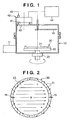
- a sputtering apparatus includes a chamber (reaction vessel) 10 which partitions and forms a processing space.
- a vacuum pump 11 is connected to the chamber 10 via a main valve (not shown) such as a gate valve.
- a disk-like substrate holder 22 which supports a disk-like substrate 21 on its upper surface is arranged at the bottom of the processing space in the chamber 10.
- the substrate 21 to be processed is carried onto the substrate holder 22 by a handling robot (not shown) via a horizontal slot (not shown).
- the substrate holder 22 is a disk-like table (stage) and, for example, electrostatically chucks and supports the substrate 21 on its upper surface.
- the substrate holder 22 is formed from a conductive member, and also functions as an electrode which generates a discharge between the substrate holder 22 and a cathode 41 (to be described later).
- the substrate holder 22 is connected to a rotational driving mechanism (not shown) and can rotate about its central axis. Along the processing surface of the substrate 21, the substrate holder 22 rotates the substrate 21 chucked and supported on the support surface.
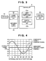
- the rotating unit or rotational driving mechanism of the substrate holder 22 includes a position detection unit (position sensor) 23 which detects the rotational position of the substrate 21 (rotational position of the substrate holder 22, or that of a magnetic field M formed by a substrate-side magnet 30 (to be described later)).
- the position detection unit 23 is, for example, a rotary encoder.
- the outer diameter of the disk-like substrate holder 22 is set larger than that of the substrate 21.
- a substrate magnetic field forming portion is arranged around the substrate 21 on the substrate holder 22 to form a magnetic field on the processing surface of the substrate 21.
- the substrate magnetic field forming portion is formed from, for example, a substrate-side magnet 30.
- the substrate-side magnet 30 is obtained by arranging a plurality of magnet pieces 31 of a permanent magnet at equal intervals at the periphery of the support surface of the substrate holder 22 in the circumferential direction of the substrate holder 22.
- the substrate-side magnet 30 can rotate together with the substrate 21 on the support surface of the substrate holder 22.
- the substrate-side magnet 30 forms, along the processing surface of the substrate 21, a uniform magnetic field having a directional property in which it faces in one direction on the processing surface.
- a dipole ring is used, and a plurality of arcuated magnet pieces 31 magnetized in different directions are combined into an annular shape so as to form the magnetic field M in one direction.
- the structure of the substrate-side magnet 30 is not limited to this, and may be an integrally molded magnet.
- the substrate-side magnet 30 may be arranged separately from the substrate holder 22 so that it can rotate in synchronism with the rotation of the substrate 21.
- the substrate-side magnet 30 is not limited to a permanent magnet, and may be an electromagnet.
- the substrate 21 is horizontally held on the support surface of the substrate holder 22.
- the substrate 21 is, for example, a disk-like silicon wafer (SiO 2 substrate), but is not limited to this.
- a cathode unit 40 including the cathode 41 which holds a target 42 is arranged diagonally above the substrate holder 22 in the processing space.
- the cathode unit 40 is arranged offset so that the center position of the cathode 41 shifts from the central axis of the substrate 21 in the plane direction of the substrate 21 and the cathode 41 is disposed at a position diagonally opposing the substrate 21.
- a magnetron including a plurality of permanent magnets is arranged on the second (face-up) surface side of the cathode 41 in the cathode unit 40 to form a magnetic field on the surface side of the target 42 attached to the first (face-down) surface of the cathode 41.
- a magnet assembly in which permanent magnets are arranged two-dimensionally may be arranged on the second surface side of the cathode 41 to form a cusped magnetic field on the surface side of the target 42.
- the plate-like target 42 is attached to the first surface of the cathode 41 of the cathode unit 40. More specifically, the target 42 is arranged on the processing space side opposite to the cathode 41, and faces down. The material of the target 42 changes depending on the type of film to be deposited on the substrate 21.
- the cathode unit 40 is electrically connected to a discharge power supply 44 which applies a discharge voltage to the cathode 41.
- the discharge power is an arbitrary one of high-frequency power, DC power, and superposition of high-frequency power and DC power.
- a discharge gas introduction system 43 is connected to the casing of the cathode unit 40 to supply a discharge process gas (discharge gas) to the vicinity of the cathode 41.
- the discharge gas is an inert gas such as Ar gas.
- the cathode 41 generates a plasma discharge between the cathode 41 and the substrate holder 22 so as to be able to sputter the target 42 attached to the cathode unit 40.
- a shutter 45 is arranged in front of the cathode unit 40 to open and close the space between the cathode unit 40 and the substrate 21.
- the shutter 45 allows pre-sputtering to remove a deposit on the surface of the target 42 before actual sputtering.
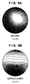
- FIG. 3 is a block diagram showing the controller 5 according to the embodiment.
- the controller 5 in the embodiment includes, for example, a general computer and various drivers.
- the controller 5 executes a film deposition processing operation in accordance with a predetermined program or an instruction from a host apparatus. More specifically, the controller 5 outputs instructions to the discharge power supply 44, the driving unit of the shutter 45, the discharge gas introduction system 43, the vacuum pump 11, the rotational driving mechanism of the substrate holder 22, and the like shown in Fig. 1 .
- a variety of process conditions are controlled, including the discharge time, discharge power, selection of the target 42, and process pressure.
- the controller 5 can also acquire the output values of sensors such as a pressure gauge (not shown) for measuring the internal pressure of the chamber 10, and the position detection unit 23 for detecting the rotational position of the substrate 21.
- the controller 5 can perform control complying with the apparatus state.
- the controller 5 includes an input power value calculation unit 51a and control signal output unit 51b.
- the input power value calculation unit 51a calculates input power to the cathode 41 to increase/decrease the film deposition amount in accordance with a rotational position detected by the position detection unit 23.
- the control signal output unit 51b outputs a control signal (e.g., voltage or current corresponding to a power value having a calculated magnitude) to adjust the power value to the calculated one.
- the controller 5 has a function of outputting a signal for controlling power applied to the cathode 41 in accordance with the rotational position of the substrate 21, based on the positional relationship between the rotational position of the substrate 21 and the cathode 41 during discharge.
- a power control unit 52 shown in Fig. 3 increases/decreases power from the discharge power supply 44 based on a control signal input from the control signal output unit 51b, and outputs, to the cathode 41, power having a magnitude calculated by the input power value calculation unit 51a.
- the cathode 41 receives discharge power corresponding to the rotational position of the substrate 21.
- the input power value is given by, for example, a sine wave function with respect to the rotational position of the substrate 21, as shown in Fig. 4 .
- the input power value calculation unit 51a can calculate an input power value by defining in advance, as a map as shown in Fig. 4 , the correspondence between the rotational position of the substrate 21 and input power to the cathode 41.
- the rotational position of the substrate 21 can be determined using, as a reference, a line segment which is parallel to the direction of the magnetic field M shown in Fig. 2 and passes through the center of the substrate 21.
- a sputtering method executed using the sputtering apparatus will be described together with the operation of the sputtering apparatus shown in Figs. 1 to 3 .
- the substrate (wafer) 21 to be processed is set on the substrate holder 22.
- the substrate 21 is carried onto the substrate holder 22 using a handling robot (not shown) via a horizontal slot (not shown).
- the vacuum pump 11 evacuates the interior of the chamber 10 to a predetermined degree of vacuum.
- the discharge gas introduction system 43 introduces a discharge gas such as Ar gas into the chamber 10.
- a magnetic field is formed on the surface of the target 42 of the cathode unit 40, and discharge power is supplied, thereby generating a plasma discharge between the target 42 and the substrate holder 22.
- the target 42 are magnetic material-containing targets such as a Co-containing target, Fe-containing target, and Ni-containing target.
- Examples of co-sputtering are those using targets made of various different magnetic materials, especially ferromagnetic materials, such as co-sputtering of Co- and Fe-containing targets to deposit a CoFe layer, and co-sputtering of Fe- and Ni-containing targets to deposit an NiFe layer.
- a target made of a magnetic material containing a diamagnetic material such as B, C, or P is also available.
- a magnetic field having a directional property in which it faces in one direction is formed on the processing surface of the substrate 21.
- the substrate 21 is rotated along its processing surface.
- the position detection unit 23 detects the rotational position of the substrate 21. Input power to the cathode 41 is adjusted in accordance with the rotational position detected by the position detection unit 23.
- FIG. 4 is a graph showing an input power control map in the sputtering method using the sputtering apparatus according to the present invention.
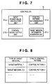
- Figs. 5 , 6A and 6B are views for explaining the principle of the embodiment.
- the controller 5 calculates discharge power to be applied to the cathode 41 as a sine wave function with respect to the rotational position of the substrate 21.
- ⁇ is 0° ⁇ ⁇ ⁇ 360°.
- A is the amplitude of input power
- ⁇ is the phase angle
- B is the center value of the amplitude of input power
- a is the regulation of input power.
- the amplitude A can be arbitrarily set as long as uniform film deposition can be implemented.
- the amplitude A can be determined in accordance with the center value B, as represented by equation (2).
- the regulation a preferably takes a value of 0.1 to 0.4. If the regulation a is excessively small, the effects of the present invention are not well obtained. If the regulation a is excessively large, it exceeds a level at which nonuniformity is canceled when speed is not changed, impairing the uniformity all the more.
- Fig. 5 shows a comparative example in which a film of a magnetic material (e.g., NiFe) is deposited by applying constant discharge power regardless of the rotational position of the substrate 21, unlike the present invention.
- the film becomes thick at a specific portion highly correlated to the formation state of a magnetic field on the processing surface of the substrate 21. More specifically, the film D gradually becomes thinner from the north pole to south pole of the substrate-side magnet 30. In this graded distribution, the film thickness difference becomes large near the centers Nc and Sc (see Fig. 2 ) of magnetic poles between the north and south poles in the circumferential direction.
- Ot is the center of the target 42.
- the scattering amount of sputtered particles becomes large at a position near the target 42 and small at a position apart from the target 42. Even when the substrate-side magnet 30 is arranged, this basic distribution remains unchanged. However, it can be considered that a portion which readily attracts sputtered particles (portion where the scattering amount of sputtered particles is large), and one which rarely attracts them are formed on the processing surface due to the formation state of a magnetic field on the processing surface of the substrate 21.
- the controller 5 controls input power to the first power value in accordance with the slanted distribution shape when the first portion where the scattering amount of sputtered particles is large due to the formation state of a magnetic field on the substrate 21 is positioned near the cathode 41 during discharge. Further, an input power control unit 52 controls input power to the second power value larger than the first power value when the second portion where the scattering amount of sputtered particles is smaller than that at the first portion is positioned near the cathode 41 during discharge.
- the controller 5 decreases input power of the substrate 21, thereby decreasing the sputtering yield and the film deposition amount at the portion where the scattering amount is large.
- the controller 5 increases the input power, thereby increasing the sputtering yield and the film deposition amount. As a result, the nonuniformity of the distribution can be canceled.
- a given point of the substrate holder 22 which rotates at a constant speed moves between a position closest to the cathode 41 and one most distant from the cathode 41.
- the power value is controlled to form a sine wave corresponding to a change of the positional relationship between the rotational position of the substrate 21 and the cathode 41 during discharge. This control is preferable because it can stably maintain plasma conditions.
- portions serving as the first and second portions change depending on, for example, the positional relationship between the cathode 41 and the substrate holder 22, the rotational speed of the substrate holder 22, and when magnetron sputtering is performed, the structure of a magnet arranged on the side of the cathode 41.
- the first and second portions are obtained in advance by an experiment or the like, and input power is controlled in accordance with them.
- a film is deposited while keeping input power constant, and the thickness distribution of the deposited film is measured.
- Figs. 6A and 6B are explanatory views each showing a sheet resistance distribution (film thickness distribution) on the substrate 21.
- Fig. 6A shows a sheet resistance distribution (embodiment) on the substrate 21 when sine wave control of input power is done.
- Fig. 6B shows a sheet resistance distribution (comparative example) when input power is kept constant during film deposition.
- the target material is NiFe
- the film deposition pressure is 0.05 Pa
- the rotational speed of the substrate 21 is 60 rpm
- the regulation a of the amplitude A of input power is 14%
- the center value B of the amplitude of input power is 4 kW.
- input power is kept constant at 4 kW, and the remaining conditions are the same as those in the embodiment.
- the in-plane distribution (1 ⁇ ) was 0.5% in the embodiment and 3.1% in the comparative example. It was confirmed that the uniformity of the in-plane distribution in the embodiment is very high.
- the magnetic field direction is a direction almost perpendicular to contours. The sheet resistance is low on the north pole side (i.e., the film thickness is large), and high on the south pole side (i.e., the film thickness is small). Note that the contours indicate normalized sheet resistance values, and the interval between them is 0.01.
- the input power control in the embodiment is not limited to sine wave control, and input power may be switched in two or more steps.
- input power may be gradually decreased to the first power as the first portion comes close to the cathode, and gradually increased to the second power as the second portion comes close to the cathode.
- the linear and quadratic functions of the rotational position or the like may be composited.
- the same sine wave control may be performed throughout film deposition, the input power control method may be changed between, for example, the initial, middle, and late stages of film deposition.
- the third portion may be obtained to set an input power different from those for the first and second portions.
- the rotational position of the substrate is not limited to a specific position, and includes a ranging rotational section (rotational position range) of the substrate.
- the magnitude of average power applied in the rotational section of the substrate may be controlled in accordance with the rotational section of the substrate.
- DC power having a predetermined magnitude or high-frequency power having a predetermined frequency may be intermittently applied to increase/decrease the input duration or interval in accordance with the rotational section of the substrate.
- the control pattern may be changed in accordance with the target material, as shown in Figs. 7 to 9 . This is because the trend of nonuniformity of the film thickness distribution changes depending on the target material.
- Fig. 7 is a block diagram showing only a controller 5. The remaining arrangement is the same as that in Fig. 3 in the first embodiment.
- a target material information acquisition unit 51c acquires information of a target material selected in film deposition as a user input, data stored in advance, or the like.
- a control pattern determination unit 51d holds a table as shown in Fig. 8 , and determines a control pattern based on target material information acquired by the target material information acquisition unit 51c.
- Fig. 9 exemplifies a control pattern.
- Fig. 9 shows the film thickness distribution of a film deposited without using the method of the present invention.
- the direction in which the film thickness increases matches the magnetic field direction.
- a position of the center Nc of the north pole in the circumferential direction with respect to the target position is defined as the rotational position ⁇ of the substrate.
- the phase ⁇ is set to 90°, though it depends on a reference position.
- the magnetic field direction and the direction in which the film thickness increases differ from each other depending on the film deposition material.
- This difference is clarified in advance as the difference angle ⁇ by an experiment or the like, and a corresponding phase ⁇ is set.
- the regulation a and the like can be set to proper values in accordance with the target material.
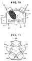
- FIG. 10 is a schematic sectional view schematically showing the sputtering apparatus according to the third embodiment.
- Fig. 10 shows a section taken along the line i - i in Fig. 11.
- Fig. 11 is a plan view schematically showing the layout relationship between a substrate holder and a cathode unit. Note that the same reference numerals as those in Fig. 1 of the first embodiment denote the same parts.
- a chamber 10 of a sputtering apparatus 1 has a gas inlet 12.
- a reactive gas introduction system 13 is connected to the gas inlet 12 to introduce a reactive process gas (reactive gas) into the chamber 10.
- the reactive gas introduction system 13 is connected to a gas cylinder (not shown) via an automatic flow controller (not shown) such as a massflow controller.
- a reactive gas is introduced via the gas inlet 12 at a predetermined flow rate.
- the reactive gas introduction system 13 supplies a reactive gas into the chamber 10.
- a plurality of cathode units 40 each including a cathode which holds a target are arranged diagonally above a substrate holder 22 in the processing space. That is, a plurality of cathode units 40 are arranged for one substrate holder 22. Each cathode unit 40 is inclined and attached to the top wall of the chamber 10.
- cathode units 40 that is, 40a to 40e are attached to the top wall of the chamber 10.
- the cathode units 40 are arranged offset at positions diagonally opposing the substrate 21 so that they are inclined with respect to the processing surface of a substrate 21 on the substrate holder 22 and are deviated at equal intervals from the central axis of the substrate 21 in directions extended from the processing surface. More specifically, the center axes of the cathodes of the cathode units 40 are positioned off the axis of rotation of the substrate holder 22, and arranged at equal intervals on a concentric circle at a predetermined distance from the axis of rotation. Since the single chamber 10 stores a plurality of cathode units 40, a multilayered structure (stack) can be deposited in one chamber 10.
- the diameter of the substrate 21 and that of the target are not particularly limited. However, when the center of the substrate 21 and that of the cathode are arranged offset and the substrate 21 is rotated as in the embodiment, uniform film deposition is possible even if the diameter of the target is smaller than that of the substrate 21.
- the five cathode units 40 are arranged, so, for example, five types of targets made of different material components can be attached. However, the present invention is not limited to this.
- each cathode unit 40 is electrically connected to a discharge power supply (not shown) which applies a discharge voltage to the cathode.
- the discharge power is an arbitrary one of high-frequency power, DC power, and superposition of high-frequency power and DC power.
- the discharge voltage is selectively applied to a plurality of cathode units 40.
- an individual discharge power supply may be connected to each cathode unit 40.
- a switching mechanism such as a switch may be adopted to selectively supply power from a common power supply.
- a shutter 45 is arranged in front of the cathode units 40 to selectively close the space between some cathodes and the substrate holder 22. By selectively opening the shutter 45, a desired target can be selected from those of the cathode units 40 to execute sputtering. The shutter 45 can prevent contamination from other sputtered targets.
- Fig. 12 is a block diagram showing the arrangements of the controller 5 and cathode units 40 according to the embodiment.
- the controller 5 shown in Fig. 12 includes an input power value calculation unit 51a and control signal output units 51b.
- the input power value calculation unit 51a calculates input power to each of cathodes 41 to increase/decrease the film deposition amount in accordance with a rotational position detected by a position detection unit 23.
- the control signal output units 51b are arranged in correspondence with the respective cathodes 41, and output a control signal (e.g., voltage or current corresponding to a power value having a calculated magnitude) to adjust the power value to the calculated one.
- a power control unit 52 of each cathode unit 40 increases/decreases power from a discharge power supply 44 based on a control signal input from the control signal output unit 51b, and outputs, to the cathode 41, power having a magnitude calculated by the input power value calculation unit 51a.
- the cathode 41 receives discharge power corresponding to the rotational position of the substrate 21.
- the input power value is given by, for example, a sine wave function with respect to the rotational position of the substrate 21, as shown in Fig. 4 .
- the input power value calculation unit 51a can calculate an input power value by defining in advance, as a map as shown in Fig. 4 , the correspondence between the rotational position of the substrate 21 and input power to the cathode 41.
- a sputtering method executed using the sputtering apparatus in the third embodiment is the same as that in the first embodiment except for the following point. That is, magnetic fields are formed on the surfaces of the targets 42 in the cathode units 40. Discharge power is supplied to generate plasma discharges between the targets 42 and the substrate holder 22, thereby co-sputtering a plurality of targets.
- the operation of the sputtering apparatus in the third embodiment is also the same as that described in the first embodiment ( Figs. 5 , 6A and 6B ).
- ⁇ is an angle formed by a specific position of the substrate and the installation position of each cathode 41 with respect to the center of rotation.
- the input power value calculation unit 51a of the controller 5 calculates the angle ⁇ for each cathode 41, and calculates the value of input power to each cathode by applying the foregoing equations (1) and (2).
- a magnetic field formed by a substrate-side magnet 30 rotates in synchronism with the substrate. Even if the substrate is rotated, the nonuniformity of the scattering amount of sputtered particles cannot be canceled, resulting in the nonuniformity of the final film thickness distribution.
- the film thickness itself may be averaged depending on the positional relationship between the cathodes 41 which simultaneously discharge.
- each target material still suffers a nonuniform distribution as described above. To solve this, the embodiment uniforms the film deposition distribution for each cathode 41 and each target 42.
- control pattern may be changed in accordance with the target material, as described with reference to Figs. 7 to 9 . This is because the trend of nonuniformity of the film thickness distribution changes depending on the target material.
- the control pattern may be changed in accordance with the positional relationship between cathodes which simultaneously discharge, as shown in Figs. 13 and 14 . This is because the trend of nonuniformity of the film thickness distribution changes depending on the interferences of an electric field and electromagnetic field formed by other cathodes.
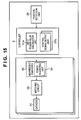
- Fig. 13 is a block diagram showing the arrangement of a controller 5. The remaining arrangement is the same as that in Fig. 3 in the first embodiment.
- a target material information acquisition unit 51c acquires information of a target material selected in film deposition as a user input, data stored in advance, or the like.
- a cathode position acquisition unit 51f acquires the positional relationship between the cathodes 41.
- a control pattern determination unit 51d holds a table as shown in Fig. 8 .
- the control pattern determination unit 51d determines a control pattern based on target material information acquired by the target material information acquisition unit 51c, and the cathode positional relationship acquired by the cathode position acquisition unit 51f.
- Fig. 14 exemplifies determination of the control pattern.
- A, B, and ⁇ in the above-described equation (1) are set to predetermined values A1, B1, and ⁇ 1. With this setting, a film with a more uniform composition can be deposited.
- the present invention is also applicable to high-frequency sputtering using a high-frequency power supply. More specifically, high-frequency power is controlled to increase/decrease the sputtering yield in accordance with the rotational position of the substrate. Also in this case, the film thickness distribution can be uniformed.
- the amplitude of high-frequency power serving as a base is changed in accordance with the rotational position of the substrate.
- the magnitude of average power per high-frequency cycle (or the magnitude of average power when the substrate falls within a predetermined rotational section) is increased/decreased.
- the sputtering yield can be adjusted in accordance with the rotational position of the substrate.
- a high-frequency power supply (e.g., 1 MHz to 300 MHz) is used.
- a control signal output unit 51b outputs a control signal to a high-frequency power supply 55.
- the high-frequency power supply 55 can supply, to a cathode 41 via a matching circuit 53, high-frequency power which is adjusted via a power adjusting unit 54.
- the control signal is obtained by a sine wave function of the amplitude with respect to the rotational position of the substrate.
- the cathode receives high-frequency power which is increased/decreased in accordance with the rotational position of the cathode.
- the central axis of the cathode 41 (target 42) in Fig. 1 is parallel to that of the substrate 21 (substrate holder 22).
- the central axis of the cathode 41 may be inclined in a direction in which the surface of the cathode 41 faces the substrate 21.
- the difference in film thickness between the first and second portions can also be canceled by increasing the rotational speed of the substrate 21 when the first portion moves on the side of the cathode 41, and decreasing it when the second portion moves on the side of the cathode 41.
- Generation of the film thickness distribution can also be suppressed by controlling both discharge power and the rotational speed of the substrate 21.
- both discharge power and the rotational speed of the substrate 21 can be controlled by sine wave control.
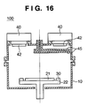
- the cathode 41 is inclined with respect to the substrate holder 22. Instead, the central axis of the cathode 41 (target 42) may be arranged parallel to that of the substrate 21 (substrate holder 22), as shown in Fig. 16 .
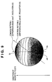
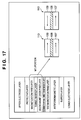
- Fig. 17 is an explanatory view showing a TMR element as an example of an electronic component which can be formed by applying the sputtering method using the sputtering apparatus according to the present invention.
- the TMR element is a magnetic effect element (TMR (Tunneling Magneto Resistance) element).
- the basic layer structure of a TMR element 110 includes an magnetic tunnel junction portion (MTJ portion) formed from a second magnetization pinned layer 107, tunnel barrier layer 108, and magnetization free layer 109.
- the second magnetization pinned layer 107 is made of a ferromagnetic material
- the tunnel barrier layer 108 is made of a metal oxide (e.g., magnesium oxide or alumina) insulating material
- the magnetization free layer 109 is made of a ferromagnetic material.
- a predetermined voltage is applied to the ferromagnetic layers on the two sides of the tunnel barrier layer 108, supplying a predetermined current.
- an external magnetic field is applied.
- the electrical resistance of the TMR element becomes minimum.
- the electrical resistance of the TMR element 110 becomes maximum.
- the magnetization of the second magnetization pinned layer 107 out of the ferromagnetic layers on the two sides is pinned.
- the direction of magnetization in the magnetization free layer 109 can be reversed by applying an external magnetic field for write.
- the film deposition step of the second magnetization pinned layer 107 sputtering film deposition is performed using the substrate-side magnet 30 to magnetize the second magnetization pinned layer 107 in a predetermined direction.
- input power is controlled to form a sine wave in accordance with the rotational position of the substrate.
- the second magnetization pinned layer 107 having a uniform sheet resistance distribution can be formed.
- the second magnetization pinned layer 107 can be made of a material which contains a ferromagnetic material such as Co, Fe, or Ni as a main component, to which a material such as B is properly added. Also in film deposition of the first magnetization pinned layer, magnetization free layer 109, and the like, in addition to the second magnetization pinned layer 107, they are magnetized in a predetermined direction using the substrate-side magnet 30. Also in this case, the present invention can be applied to form films each exhibiting a uniform sheet resistance distribution.
Landscapes
- Chemical & Material Sciences (AREA)
- Engineering & Computer Science (AREA)
- Physics & Mathematics (AREA)
- Analytical Chemistry (AREA)
- Plasma & Fusion (AREA)
- Mechanical Engineering (AREA)
- Organic Chemistry (AREA)
- Metallurgy (AREA)
- Materials Engineering (AREA)
- Chemical Kinetics & Catalysis (AREA)
- Power Engineering (AREA)
- Nanotechnology (AREA)
- Manufacturing & Machinery (AREA)
- Crystallography & Structural Chemistry (AREA)
- Physical Vapour Deposition (AREA)
- Magnetic Heads (AREA)
- Thin Magnetic Films (AREA)
- Hall/Mr Elements (AREA)
Claims (14)
- Sputtervorrichtung für magnetisches Material, gekennzeichnet durch
einen Substrathalter (22), der ein Substrat (21) hält, um in einer Ebenenrichtung einer Verarbeitungsoberfläche des Substrats (21) rotierbar zu sein,
einer Substratmagnetfeldbildungseinrichtung (30), die um das Substrat (21) herum angeordnet ist und synchron mit dem Substrat (21) rotierbar ist, zur Bildung eines Magnetfeldes (M) mit einer Richtungseigenschaft entlang der Verarbeitungsoberfläche des Substrats (21) an der Verarbeitungsoberfläche des Substrats (21),
eine Kathode (41), die an einer Position diagonal gegenüber dem Substrat (21) angeordnet ist und eine Entladungsenergie empfängt,
eine Positionserfassungseinrichtung (23) zur Erfassung einer Rotationsposition des Substrats (21), und
eine Energiesteuereinrichtung (52) zur Steuerung einer an die Kathode (41) angelegten Energie gemäß der durch die Positionserfassungseinrichtung (23) erfassten Rotationsposition. - Sputtervorrichtung nach Anspruch 1, dadurch gekennzeichnet, dass die Energiesteuereinrichtung (52) Energie basierend auf einer Positionsbeziehung zwischen einer bestimmten Position des Substrats (21) und der Kathode (41) steuert.
- Sputtervorrichtung nach Anspruch 2, dadurch gekennzeichnet, dass die Energiesteuereinrichtung (52) eine erste Energie anlegt, wenn ein erster Abschnitt, bei dem ein Streuungsausmaß von gesputterten Partikeln aufgrund eines Bildungszustands eines Magnetfeldes (M) an dem Substrat (21) groß ist, nahe der Kathode (41) positioniert ist, und eine zweite Energie größer als die erste Energie anlegt, wenn ein zweiter Abschnitt, bei dem das Streuungsausmaß von gesputterten Partikeln kleiner als das Streuungsausmaß von gesputterten Partikeln an dem ersten Abschnitt ist, nahe der Kathode (41) positioniert ist.
- Sputtervorrichtung nach Anspruch 3, dadurch gekennzeichnet, dass die Energiesteuereinrichtung (52) allmählich eine Eingabeenergie zu der ersten Energie verringert, wenn sich der erste Abschnitt der Kathode (41) nähert, und allmählich die Eingabeenergie zu der zweiten Energie erhöht, wenn sich der zweite Abschnitt der Kathode (41) nähert.
- Sputtervorrichtung nach Anspruch 1, ferner gekennzeichnet durch
eine Vielzahl von Kathoden (41), die jeweils an Positionen diagonal gegenüber dem Substrat (21) angeordnet sind und Entladungsenergie empfangen,
eine Vielzahl von Energiesteuereinrichtungen (52), die entsprechend der jeweiligen Kathoden (41) angeordnet sind, wobei jede für eine Steuerung von an die entsprechende Kathode (41) angelegte Energie gemäß der durch die Positionserfassungseinrichtung (23) erfassten Rotationsposition eingerichtet ist, und
eine Filmablagerungssteuereinrichtung (5) zur Ausführung einer Filmablagerung durch Mitsputtern für das mittels des Substrathalters (22) gehaltenen Substrats (21) durch Anlegen einer Entladungsenergie an die Vielzahl von Kathoden (41) über die Vielzahl von Energiesteuereinrichtungen (52). - Sputtervorrichtung nach Anspruch 5, dadurch gekennzeichnet, dass die Energiesteuereinrichtung (52) Energie basierend auf einer Positionsbeziehung zwischen einer bestimmten Position des Substrats (21) und der entsprechenden Kathode (41) steuert.
- Sputtervorrichtung nach Anspruch 6, dadurch gekennzeichnet, dass die Energiesteuereinrichtung (52) eine erste Energie anlegt, wenn ein erster Abschnitt, bei dem ein Streuungsausmaß von gesputterten Partikeln aufgrund eines Bildungszustands eines Magnetfeldes (M) an dem Substrat (21) groß ist, nahe der entsprechenden Kathode (41) positioniert ist, und eine zweite Energie größer als die erste Energie anlegt, wenn ein zweiter Abschnitt, bei dem das Streuungsausmaß von gesputterten Partikeln kleiner als das Streuungsausmaß von gesputterten Partikeln an dem ersten Abschnitt ist, nahe der entsprechenden Kathode (41) positioniert ist.
- Sputtervorrichtung nach Anspruch 7, dadurch gekennzeichnet, dass die Energiesteuereinrichtung (52) allmählich eine Eingabeenergie zu der ersten Energie verringert, wenn sich der erste Abschnitt der entsprechenden Kathode (41) nähert, und allmählich die Eingabeenergie zu der zweiten Energie erhöht, wenn sich der zweite Abschnitt der entsprechenden Kathode (41) nähert.
- Sputtervorrichtung nach Anspruch 5, dadurch gekennzeichnet, dass die Energiesteuereinrichtung (52) die an die entsprechende Kathode (41) angelegte Energie basierend auf einem gemäß einem zu sputternden Zielmaterial eingestellten Steuermuster anpasst.
- Sputtervorrichtung nach Anspruch 5, dadurch gekennzeichnet, dass die Energiesteuereinrichtung (52) die an die entsprechende Kathode (41) angelegte Energie basierend auf einem gemäß einer Positionsbeziehung zwischen der entsprechenden Kathode (41) und den verbleibenden Kathoden (41) eingestellten Steuermuster anpasst.
- Sputterverfahren für magnetisches Material, gekennzeichnet durch ein Ausführen eines Filmablagerns durch Anlegen, an eine an einer Position diagonal gegenüber einem Substrat (21) angeordnete Kathode (41), einer Energie, die gemäß einer mittels einer Positionserfassungseinrichtung (23) erfassten Rotationsposition des Substrats (21) angepasst ist, während eines Rotierens des Substrats (21) in einer Ebenenrichtung einer Verarbeitungsoberfläche des Substrats (21), und Bilden eines Magnetfeldes (M), das synchron mit dem Substrat (21) rotiert und eine Richtungseigenschaft entlang der Verarbeitungsoberfläche des Substrats (21) aufweist, an der Verarbeitungsoberfläche.
- Verfahren nach Anspruch 11 zum Ablagern eines Films in einem Film-ablagerungsschritt bei einer Herstellung eines elektronischen Geräts.
- Sputterverfahren nach Anspruch 11, wobei das Filmablagern ausgeführt wird durch Mitsputtern durch Anlegen, an eine Vielzahl der Kathoden (41), die an Positionen diagonal gegenüber dem Substrat (21) angeordnet sind und Ziele (42) halten, die aus verschiedenen Materialien gebildet sind, einer Energie, die gemäß einer mittels einer Positionserfassungseinrichtung (23) erfassten Rotationsposition des Substrats (21) angepasst ist, während eines Rotierens des Substrats (21) in einer Ebenenrichtung einer Verarbeitungsoberfläche des Substrats (21), und Bilden eines Magnetfeldes (M) an der Verarbeitungsoberfläche.
- Verfahren nach Anspruch 12, wobei das Filmablagern ausgeführt wird durch Mitsputtern durch Anlegen, an eine Vielzahl der Kathoden (41), die an Positionen diagonal gegenüber dem Substrat (21) angeordnet sind und Ziele (42) halten, die aus verschiedenen Materialien gebildet sind, einer Energie, die gemäß einer mittels einer Positionserfassungseinrichtung (23) erfassten Rotationsposition des Substrats (21) angepasst ist, während eines Rotierens des Substrats (21) in einer Ebenenrichtung einer Verarbeitungsoberfläche des Substrats (21), und Bilden eines Magnetfeldes (M) an der Verarbeitungsoberfläche.
Applications Claiming Priority (3)
| Application Number | Priority Date | Filing Date | Title |
|---|---|---|---|
| JP2008333480 | 2008-12-26 | ||
| JP2008333066 | 2008-12-26 | ||
| PCT/JP2009/007278 WO2010073711A1 (ja) | 2008-12-26 | 2009-12-25 | スパッタリング装置、スパッタリング方法及び電子デバイスの製造方法 |
Publications (3)
| Publication Number | Publication Date |
|---|---|
| EP2390380A1 EP2390380A1 (de) | 2011-11-30 |
| EP2390380A4 EP2390380A4 (de) | 2014-01-08 |
| EP2390380B1 true EP2390380B1 (de) | 2016-03-09 |
Family
ID=42287344
Family Applications (1)
| Application Number | Title | Priority Date | Filing Date |
|---|---|---|---|
| EP09834517.6A Active EP2390380B1 (de) | 2008-12-26 | 2009-12-25 | Sputtereinrichtung, sputterverfahren und verfahren zur herstellung einer elektronischen vorrichtung |
Country Status (6)
| Country | Link |
|---|---|
| US (1) | US8906208B2 (de) |
| EP (1) | EP2390380B1 (de) |
| JP (2) | JP4739464B2 (de) |
| KR (2) | KR101272009B1 (de) |
| CN (1) | CN102227514B (de) |
| WO (1) | WO2010073711A1 (de) |
Families Citing this family (24)
| Publication number | Priority date | Publication date | Assignee | Title |
|---|---|---|---|---|
| WO2010038421A1 (ja) * | 2008-09-30 | 2010-04-08 | キヤノンアネルバ株式会社 | スパッタリング装置及びスパッタリング方法 |
| CN102227514B (zh) * | 2008-12-26 | 2014-08-20 | 佳能安内华股份有限公司 | 溅射装置、溅射方法和电子器件制造方法 |
| JP6023722B2 (ja) * | 2011-12-22 | 2016-11-09 | キヤノンアネルバ株式会社 | SrRuO3膜の成膜方法 |
| JP5806967B2 (ja) * | 2012-03-30 | 2015-11-10 | 株式会社クボタ | ディーゼルエンジンの排気処理装置 |
| CN103374705B (zh) * | 2012-04-11 | 2015-12-02 | 北京北方微电子基地设备工艺研究中心有限责任公司 | 一种磁控溅射装置 |
| US20130327634A1 (en) * | 2012-06-08 | 2013-12-12 | Chang-Beom Eom | Misaligned sputtering systems for the deposition of complex oxide thin films |
| US20150114826A1 (en) * | 2012-06-18 | 2015-04-30 | Oerlikon Advanced Technologies Ag | Pvd apparatus for directional material deposition, methods and workpiece |
| JP2014046231A (ja) | 2012-08-29 | 2014-03-17 | Hitachi Chemical Co Ltd | カーボンナノチューブ合成用触媒の製造方法 |
| KR101375878B1 (ko) * | 2012-09-27 | 2014-03-17 | 한국생산기술연구원 | 미세패턴 형성 방법 |
| US10048157B2 (en) * | 2013-07-11 | 2018-08-14 | Android Industries Llc | Balancing device, uniformity device and methods for utilizing the same |
| CN103487311B (zh) * | 2013-09-11 | 2016-04-13 | 广东省东莞市质量监督检测中心 | 一种湿浆样品置放装置及其控制方法 |
| US10196734B2 (en) * | 2014-03-25 | 2019-02-05 | Iowa State University Research Foundation, Inc. | Nanotwinned silver alloy film with controlled architecture |
| CN105112864B (zh) * | 2015-08-13 | 2019-03-05 | 江苏时代全芯存储科技有限公司 | 镀膜装置 |
| WO2017098537A1 (ja) * | 2015-12-07 | 2017-06-15 | キヤノンアネルバ株式会社 | 磁気抵抗効果素子の製造方法および装置 |
| US10431440B2 (en) * | 2015-12-20 | 2019-10-01 | Applied Materials, Inc. | Methods and apparatus for processing a substrate |
| JP6498261B1 (ja) * | 2017-12-05 | 2019-04-10 | 昭和電工株式会社 | 磁気センサの製造方法及び磁気センサ集合体 |
| JP7120857B2 (ja) * | 2018-05-10 | 2022-08-17 | 株式会社アルバック | 抵抗体膜の製造方法及び抵抗体膜 |
| DE102019200761A1 (de) * | 2019-01-22 | 2020-07-23 | TRUMPF Hüttinger GmbH + Co. KG | Verfahren zur Kompensation von Prozessschwankungen eines Plasmaprozesses und Regler für einen Leistungsgenerator zur Versorgung eines Plasmaprozesses |
| US11557473B2 (en) * | 2019-04-19 | 2023-01-17 | Applied Materials, Inc. | System and method to control PVD deposition uniformity |
| TW202104628A (zh) | 2019-04-19 | 2021-02-01 | 美商應用材料股份有限公司 | 用於控制pvd沉積均勻性的系統及方法 |
| EP3987079A4 (de) | 2019-06-24 | 2023-03-01 | TRUMPF Huettinger Sp. Z o. o. | Verfahren zur einstellung der ausgangsleistung einer stromversorgung für ein plasma, plasmagerät und stromversorgung |
| KR102923867B1 (ko) * | 2019-07-09 | 2026-02-04 | 삼성전자주식회사 | 스퍼터링 장치 및 이를 이용한 반도체 장치의 제조 방법 |
| CN110344013B (zh) * | 2019-08-19 | 2025-05-23 | 北京北方华创微电子装备有限公司 | 溅射方法 |
| WO2026022386A1 (de) * | 2024-07-25 | 2026-01-29 | Fhr Anlagenbau Gmbh | Vakuumbeschichtungsanlage mit mehreren quellenanordnungen |
Family Cites Families (19)
| Publication number | Priority date | Publication date | Assignee | Title |
|---|---|---|---|---|
| JPS60207270A (ja) * | 1984-03-30 | 1985-10-18 | 日本航空電子工業株式会社 | コネクタ |
| US4607903A (en) * | 1984-03-30 | 1986-08-26 | Japan Aviation Electronics Industry Limited | Connector assembly |
| JPS61250163A (ja) * | 1985-04-26 | 1986-11-07 | Nippon Telegr & Teleph Corp <Ntt> | 多層薄膜の製造方法および装置 |
| US6290824B1 (en) * | 1992-10-28 | 2001-09-18 | Hitachi, Ltd. | Magnetic film forming system |
| US6491802B2 (en) * | 1992-10-28 | 2002-12-10 | Hitachi, Ltd. | Magnetic film forming system |
| JP2824001B2 (ja) * | 1993-01-07 | 1998-11-11 | 株式会社日立製作所 | 磁性膜形成装置 |
| JPH0969460A (ja) * | 1995-09-01 | 1997-03-11 | Kao Corp | 磁気記録媒体の製造方法 |
| JP4223614B2 (ja) | 1999-01-12 | 2009-02-12 | キヤノンアネルバ株式会社 | スパッタリング方法及び装置及び電子部品の製造方法 |
| JP4205294B2 (ja) * | 2000-08-01 | 2009-01-07 | キヤノンアネルバ株式会社 | 基板処理装置及び方法 |
| JP2002069631A (ja) * | 2000-08-24 | 2002-03-08 | Hitachi Ltd | スパッタ方法及びその装置 |
| JP3505135B2 (ja) * | 2000-08-30 | 2004-03-08 | 株式会社日鉱マテリアルズ | 銅の表面処理方法 |
| JP2002167661A (ja) * | 2000-11-30 | 2002-06-11 | Anelva Corp | 磁性多層膜作製装置 |
| US7381661B2 (en) * | 2002-10-15 | 2008-06-03 | Oc Oerlikon Balzers Ag | Method for the production of a substrate with a magnetron sputter coating and unit for the same |
| US20050103620A1 (en) * | 2003-11-19 | 2005-05-19 | Zond, Inc. | Plasma source with segmented magnetron cathode |
| JP4494047B2 (ja) * | 2004-03-12 | 2010-06-30 | キヤノンアネルバ株式会社 | 多元スパッタ成膜装置の二重シャッタ制御方法 |
| JP4473323B2 (ja) * | 2007-04-26 | 2010-06-02 | キヤノンアネルバ株式会社 | スパッタリング成膜方法、電子デバイスの製造方法及びスパッタリング装置 |
| WO2009157341A1 (ja) * | 2008-06-25 | 2009-12-30 | キヤノンアネルバ株式会社 | スパッタリング装置及びその制御用プログラムを記録した記録媒体 |
| WO2010038421A1 (ja) | 2008-09-30 | 2010-04-08 | キヤノンアネルバ株式会社 | スパッタリング装置及びスパッタリング方法 |
| CN102227514B (zh) * | 2008-12-26 | 2014-08-20 | 佳能安内华股份有限公司 | 溅射装置、溅射方法和电子器件制造方法 |
-
2009
- 2009-12-25 CN CN200980147190.7A patent/CN102227514B/zh active Active
- 2009-12-25 JP JP2010522884A patent/JP4739464B2/ja active Active
- 2009-12-25 KR KR1020117014654A patent/KR101272009B1/ko active Active
- 2009-12-25 EP EP09834517.6A patent/EP2390380B1/de active Active
- 2009-12-25 KR KR1020137002927A patent/KR101271843B1/ko active Active
- 2009-12-25 WO PCT/JP2009/007278 patent/WO2010073711A1/ja not_active Ceased
-
2011
- 2011-04-25 JP JP2011097548A patent/JP5587822B2/ja active Active
- 2011-05-10 US US13/104,472 patent/US8906208B2/en active Active
Also Published As
| Publication number | Publication date |
|---|---|
| WO2010073711A1 (ja) | 2010-07-01 |
| US8906208B2 (en) | 2014-12-09 |
| JPWO2010073711A1 (ja) | 2012-06-14 |
| KR101271843B1 (ko) | 2013-06-07 |
| KR20110089878A (ko) | 2011-08-09 |
| JP5587822B2 (ja) | 2014-09-10 |
| US20110209986A1 (en) | 2011-09-01 |
| KR20130019035A (ko) | 2013-02-25 |
| JP4739464B2 (ja) | 2011-08-03 |
| EP2390380A1 (de) | 2011-11-30 |
| EP2390380A4 (de) | 2014-01-08 |
| JP2011149104A (ja) | 2011-08-04 |
| CN102227514B (zh) | 2014-08-20 |
| CN102227514A (zh) | 2011-10-26 |
| KR101272009B1 (ko) | 2013-06-05 |
Similar Documents
| Publication | Publication Date | Title |
|---|---|---|
| EP2390380B1 (de) | Sputtereinrichtung, sputterverfahren und verfahren zur herstellung einer elektronischen vorrichtung | |
| CN102171379B (zh) | 溅射装置以及溅射方法 | |
| US6258217B1 (en) | Rotating magnet array and sputter source | |
| CN103374705B (zh) | 一种磁控溅射装置 | |
| EP2586889A1 (de) | Sputtervorrichtung, abscheidungsverfahren und steuervorrichtung | |
| JP5059430B2 (ja) | スパッタ方法及びスパッタ装置 | |
| US20090277779A1 (en) | Magnetic field generating apparatus, magnetic field generating method, sputtering apparatus, and method of manufacturing device | |
| US20110220494A1 (en) | Methods and apparatus for magnetron metallization for semiconductor fabrication | |
| CN104810228B (zh) | 螺旋形磁控管及磁控溅射设备 | |
| EP2317537A1 (de) | Sputterauftragungssystem und -verfahren | |
| US20250112032A1 (en) | Permeance magnetic assembly | |
| JP2016011445A (ja) | スパッタリング方法 | |
| US8852412B2 (en) | Magnetron source and method of manufacturing | |
| JP2000045069A (ja) | マグネトロンスパッタリング装置及びスパッタリング方法 |
Legal Events
| Date | Code | Title | Description |
|---|---|---|---|
| PUAI | Public reference made under article 153(3) epc to a published international application that has entered the european phase |
Free format text: ORIGINAL CODE: 0009012 |
|
| 17P | Request for examination filed |
Effective date: 20110419 |
|
| AK | Designated contracting states |
Kind code of ref document: A1 Designated state(s): AT BE BG CH CY CZ DE DK EE ES FI FR GB GR HR HU IE IS IT LI LT LU LV MC MK MT NL NO PL PT RO SE SI SK SM TR |
|
| DAX | Request for extension of the european patent (deleted) | ||
| A4 | Supplementary search report drawn up and despatched |
Effective date: 20131205 |
|
| RIC1 | Information provided on ipc code assigned before grant |
Ipc: C23C 14/54 20060101ALI20131129BHEP Ipc: H01L 43/12 20060101ALI20131129BHEP Ipc: H01J 37/34 20060101ALI20131129BHEP Ipc: H01L 43/08 20060101ALI20131129BHEP Ipc: C23C 14/34 20060101AFI20131129BHEP Ipc: H01F 41/18 20060101ALI20131129BHEP |
|
| 17Q | First examination report despatched |
Effective date: 20150226 |
|
| GRAP | Despatch of communication of intention to grant a patent |
Free format text: ORIGINAL CODE: EPIDOSNIGR1 |
|
| INTG | Intention to grant announced |
Effective date: 20150813 |
|
| GRAS | Grant fee paid |
Free format text: ORIGINAL CODE: EPIDOSNIGR3 |
|
| GRAA | (expected) grant |
Free format text: ORIGINAL CODE: 0009210 |
|
| AK | Designated contracting states |
Kind code of ref document: B1 Designated state(s): AT BE BG CH CY CZ DE DK EE ES FI FR GB GR HR HU IE IS IT LI LT LU LV MC MK MT NL NO PL PT RO SE SI SK SM TR |
|
| REG | Reference to a national code |
Ref country code: GB Ref legal event code: FG4D |
|
| REG | Reference to a national code |
Ref country code: AT Ref legal event code: REF Ref document number: 779603 Country of ref document: AT Kind code of ref document: T Effective date: 20160315 Ref country code: CH Ref legal event code: EP |
|
| REG | Reference to a national code |
Ref country code: IE Ref legal event code: FG4D |
|
| REG | Reference to a national code |
Ref country code: DE Ref legal event code: R096 Ref document number: 602009036730 Country of ref document: DE |
|
| REG | Reference to a national code |
Ref country code: LT Ref legal event code: MG4D |
|
| REG | Reference to a national code |
Ref country code: NL Ref legal event code: MP Effective date: 20160309 |
|
| PG25 | Lapsed in a contracting state [announced via postgrant information from national office to epo] |
Ref country code: ES Free format text: LAPSE BECAUSE OF FAILURE TO SUBMIT A TRANSLATION OF THE DESCRIPTION OR TO PAY THE FEE WITHIN THE PRESCRIBED TIME-LIMIT Effective date: 20160309 Ref country code: FI Free format text: LAPSE BECAUSE OF FAILURE TO SUBMIT A TRANSLATION OF THE DESCRIPTION OR TO PAY THE FEE WITHIN THE PRESCRIBED TIME-LIMIT Effective date: 20160309 Ref country code: HR Free format text: LAPSE BECAUSE OF FAILURE TO SUBMIT A TRANSLATION OF THE DESCRIPTION OR TO PAY THE FEE WITHIN THE PRESCRIBED TIME-LIMIT Effective date: 20160309 Ref country code: NO Free format text: LAPSE BECAUSE OF FAILURE TO SUBMIT A TRANSLATION OF THE DESCRIPTION OR TO PAY THE FEE WITHIN THE PRESCRIBED TIME-LIMIT Effective date: 20160609 Ref country code: GR Free format text: LAPSE BECAUSE OF FAILURE TO SUBMIT A TRANSLATION OF THE DESCRIPTION OR TO PAY THE FEE WITHIN THE PRESCRIBED TIME-LIMIT Effective date: 20160610 |
|
| REG | Reference to a national code |
Ref country code: AT Ref legal event code: MK05 Ref document number: 779603 Country of ref document: AT Kind code of ref document: T Effective date: 20160309 |
|
| PG25 | Lapsed in a contracting state [announced via postgrant information from national office to epo] |
Ref country code: SE Free format text: LAPSE BECAUSE OF FAILURE TO SUBMIT A TRANSLATION OF THE DESCRIPTION OR TO PAY THE FEE WITHIN THE PRESCRIBED TIME-LIMIT Effective date: 20160309 Ref country code: LV Free format text: LAPSE BECAUSE OF FAILURE TO SUBMIT A TRANSLATION OF THE DESCRIPTION OR TO PAY THE FEE WITHIN THE PRESCRIBED TIME-LIMIT Effective date: 20160309 Ref country code: LT Free format text: LAPSE BECAUSE OF FAILURE TO SUBMIT A TRANSLATION OF THE DESCRIPTION OR TO PAY THE FEE WITHIN THE PRESCRIBED TIME-LIMIT Effective date: 20160309 Ref country code: NL Free format text: LAPSE BECAUSE OF FAILURE TO SUBMIT A TRANSLATION OF THE DESCRIPTION OR TO PAY THE FEE WITHIN THE PRESCRIBED TIME-LIMIT Effective date: 20160309 Ref country code: PL Free format text: LAPSE BECAUSE OF FAILURE TO SUBMIT A TRANSLATION OF THE DESCRIPTION OR TO PAY THE FEE WITHIN THE PRESCRIBED TIME-LIMIT Effective date: 20160309 |
|
| PG25 | Lapsed in a contracting state [announced via postgrant information from national office to epo] |
Ref country code: IS Free format text: LAPSE BECAUSE OF FAILURE TO SUBMIT A TRANSLATION OF THE DESCRIPTION OR TO PAY THE FEE WITHIN THE PRESCRIBED TIME-LIMIT Effective date: 20160709 Ref country code: EE Free format text: LAPSE BECAUSE OF FAILURE TO SUBMIT A TRANSLATION OF THE DESCRIPTION OR TO PAY THE FEE WITHIN THE PRESCRIBED TIME-LIMIT Effective date: 20160309 |
|
| PG25 | Lapsed in a contracting state [announced via postgrant information from national office to epo] |
Ref country code: SM Free format text: LAPSE BECAUSE OF FAILURE TO SUBMIT A TRANSLATION OF THE DESCRIPTION OR TO PAY THE FEE WITHIN THE PRESCRIBED TIME-LIMIT Effective date: 20160309 Ref country code: PT Free format text: LAPSE BECAUSE OF FAILURE TO SUBMIT A TRANSLATION OF THE DESCRIPTION OR TO PAY THE FEE WITHIN THE PRESCRIBED TIME-LIMIT Effective date: 20160711 Ref country code: RO Free format text: LAPSE BECAUSE OF FAILURE TO SUBMIT A TRANSLATION OF THE DESCRIPTION OR TO PAY THE FEE WITHIN THE PRESCRIBED TIME-LIMIT Effective date: 20160309 Ref country code: AT Free format text: LAPSE BECAUSE OF FAILURE TO SUBMIT A TRANSLATION OF THE DESCRIPTION OR TO PAY THE FEE WITHIN THE PRESCRIBED TIME-LIMIT Effective date: 20160309 Ref country code: CZ Free format text: LAPSE BECAUSE OF FAILURE TO SUBMIT A TRANSLATION OF THE DESCRIPTION OR TO PAY THE FEE WITHIN THE PRESCRIBED TIME-LIMIT Effective date: 20160309 Ref country code: SK Free format text: LAPSE BECAUSE OF FAILURE TO SUBMIT A TRANSLATION OF THE DESCRIPTION OR TO PAY THE FEE WITHIN THE PRESCRIBED TIME-LIMIT Effective date: 20160309 |
|
| REG | Reference to a national code |
Ref country code: DE Ref legal event code: R097 Ref document number: 602009036730 Country of ref document: DE |
|
| PG25 | Lapsed in a contracting state [announced via postgrant information from national office to epo] |
Ref country code: IT Free format text: LAPSE BECAUSE OF FAILURE TO SUBMIT A TRANSLATION OF THE DESCRIPTION OR TO PAY THE FEE WITHIN THE PRESCRIBED TIME-LIMIT Effective date: 20160309 Ref country code: BE Free format text: LAPSE BECAUSE OF FAILURE TO SUBMIT A TRANSLATION OF THE DESCRIPTION OR TO PAY THE FEE WITHIN THE PRESCRIBED TIME-LIMIT Effective date: 20160309 |
|
| PLBE | No opposition filed within time limit |
Free format text: ORIGINAL CODE: 0009261 |
|
| STAA | Information on the status of an ep patent application or granted ep patent |
Free format text: STATUS: NO OPPOSITION FILED WITHIN TIME LIMIT |
|
| PG25 | Lapsed in a contracting state [announced via postgrant information from national office to epo] |
Ref country code: DK Free format text: LAPSE BECAUSE OF FAILURE TO SUBMIT A TRANSLATION OF THE DESCRIPTION OR TO PAY THE FEE WITHIN THE PRESCRIBED TIME-LIMIT Effective date: 20160309 |
|
| 26N | No opposition filed |
Effective date: 20161212 |
|
| PG25 | Lapsed in a contracting state [announced via postgrant information from national office to epo] |
Ref country code: BG Free format text: LAPSE BECAUSE OF FAILURE TO SUBMIT A TRANSLATION OF THE DESCRIPTION OR TO PAY THE FEE WITHIN THE PRESCRIBED TIME-LIMIT Effective date: 20160609 |
|
| PG25 | Lapsed in a contracting state [announced via postgrant information from national office to epo] |
Ref country code: SI Free format text: LAPSE BECAUSE OF FAILURE TO SUBMIT A TRANSLATION OF THE DESCRIPTION OR TO PAY THE FEE WITHIN THE PRESCRIBED TIME-LIMIT Effective date: 20160309 |
|
| REG | Reference to a national code |
Ref country code: DE Ref legal event code: R119 Ref document number: 602009036730 Country of ref document: DE |
|
| REG | Reference to a national code |
Ref country code: CH Ref legal event code: PL |
|
| PG25 | Lapsed in a contracting state [announced via postgrant information from national office to epo] |
Ref country code: MC Free format text: LAPSE BECAUSE OF FAILURE TO SUBMIT A TRANSLATION OF THE DESCRIPTION OR TO PAY THE FEE WITHIN THE PRESCRIBED TIME-LIMIT Effective date: 20160309 |
|
| REG | Reference to a national code |
Ref country code: FR Ref legal event code: ST Effective date: 20170831 |
|
| REG | Reference to a national code |
Ref country code: IE Ref legal event code: MM4A |
|
| PG25 | Lapsed in a contracting state [announced via postgrant information from national office to epo] |
Ref country code: LU Free format text: LAPSE BECAUSE OF NON-PAYMENT OF DUE FEES Effective date: 20161225 Ref country code: FR Free format text: LAPSE BECAUSE OF NON-PAYMENT OF DUE FEES Effective date: 20170102 Ref country code: LI Free format text: LAPSE BECAUSE OF NON-PAYMENT OF DUE FEES Effective date: 20161231 Ref country code: CH Free format text: LAPSE BECAUSE OF NON-PAYMENT OF DUE FEES Effective date: 20161231 |
|
| PG25 | Lapsed in a contracting state [announced via postgrant information from national office to epo] |
Ref country code: DE Free format text: LAPSE BECAUSE OF NON-PAYMENT OF DUE FEES Effective date: 20170701 Ref country code: IE Free format text: LAPSE BECAUSE OF NON-PAYMENT OF DUE FEES Effective date: 20161225 |
|
| PG25 | Lapsed in a contracting state [announced via postgrant information from national office to epo] |
Ref country code: HU Free format text: LAPSE BECAUSE OF FAILURE TO SUBMIT A TRANSLATION OF THE DESCRIPTION OR TO PAY THE FEE WITHIN THE PRESCRIBED TIME-LIMIT; INVALID AB INITIO Effective date: 20091225 Ref country code: CY Free format text: LAPSE BECAUSE OF FAILURE TO SUBMIT A TRANSLATION OF THE DESCRIPTION OR TO PAY THE FEE WITHIN THE PRESCRIBED TIME-LIMIT Effective date: 20160309 |
|
| PG25 | Lapsed in a contracting state [announced via postgrant information from national office to epo] |
Ref country code: TR Free format text: LAPSE BECAUSE OF FAILURE TO SUBMIT A TRANSLATION OF THE DESCRIPTION OR TO PAY THE FEE WITHIN THE PRESCRIBED TIME-LIMIT Effective date: 20160309 Ref country code: MK Free format text: LAPSE BECAUSE OF FAILURE TO SUBMIT A TRANSLATION OF THE DESCRIPTION OR TO PAY THE FEE WITHIN THE PRESCRIBED TIME-LIMIT Effective date: 20160309 |
|
| PG25 | Lapsed in a contracting state [announced via postgrant information from national office to epo] |
Ref country code: MT Free format text: LAPSE BECAUSE OF NON-PAYMENT OF DUE FEES Effective date: 20161225 |
|
| PGFP | Annual fee paid to national office [announced via postgrant information from national office to epo] |
Ref country code: GB Payment date: 20251114 Year of fee payment: 17 |