EP2365529B1 - Affichage d'écran AMOLED avec compensation optique de réaction - Google Patents
Affichage d'écran AMOLED avec compensation optique de réaction Download PDFInfo
- Publication number
- EP2365529B1 EP2365529B1 EP10172977.0A EP10172977A EP2365529B1 EP 2365529 B1 EP2365529 B1 EP 2365529B1 EP 10172977 A EP10172977 A EP 10172977A EP 2365529 B1 EP2365529 B1 EP 2365529B1
- Authority
- EP
- European Patent Office
- Prior art keywords
- oled
- layer
- transistor
- electrically coupled
- gate
- Prior art date
- Legal status (The legal status is an assumption and is not a legal conclusion. Google has not performed a legal analysis and makes no representation as to the accuracy of the status listed.)
- Active
Links
- 229920001621 AMOLED Polymers 0.000 title claims description 43
- 230000003287 optical effect Effects 0.000 title description 8
- 239000003990 capacitor Substances 0.000 claims description 3
- 239000010410 layer Substances 0.000 description 138
- 239000002184 metal Substances 0.000 description 21
- 229910052751 metal Inorganic materials 0.000 description 21
- 239000004065 semiconductor Substances 0.000 description 13
- 239000000758 substrate Substances 0.000 description 13
- 238000002161 passivation Methods 0.000 description 10
- 239000011229 interlayer Substances 0.000 description 9
- 229910004205 SiNX Inorganic materials 0.000 description 8
- 229910052814 silicon oxide Inorganic materials 0.000 description 8
- VYPSYNLAJGMNEJ-UHFFFAOYSA-N Silicium dioxide Chemical compound O=[Si]=O VYPSYNLAJGMNEJ-UHFFFAOYSA-N 0.000 description 7
- 230000007547 defect Effects 0.000 description 6
- 239000012212 insulator Substances 0.000 description 6
- 239000000463 material Substances 0.000 description 6
- 238000000034 method Methods 0.000 description 5
- 238000010586 diagram Methods 0.000 description 4
- 229910021420 polycrystalline silicon Inorganic materials 0.000 description 4
- 229910052802 copper Inorganic materials 0.000 description 3
- 239000011159 matrix material Substances 0.000 description 3
- 239000011368 organic material Substances 0.000 description 3
- 239000010409 thin film Substances 0.000 description 3
- 229910017107 AlOx Inorganic materials 0.000 description 2
- 230000007423 decrease Effects 0.000 description 2
- 230000009189 diving Effects 0.000 description 2
- 238000004519 manufacturing process Methods 0.000 description 2
- 229920005591 polysilicon Polymers 0.000 description 2
- 229910017150 AlTi Inorganic materials 0.000 description 1
- XUIMIQQOPSSXEZ-UHFFFAOYSA-N Silicon Chemical compound [Si] XUIMIQQOPSSXEZ-UHFFFAOYSA-N 0.000 description 1
- 229910021417 amorphous silicon Inorganic materials 0.000 description 1
- 238000003491 array Methods 0.000 description 1
- 239000000919 ceramic Substances 0.000 description 1
- 238000009295 crossflow filtration Methods 0.000 description 1
- 238000002425 crystallisation Methods 0.000 description 1
- 230000008025 crystallization Effects 0.000 description 1
- 230000007812 deficiency Effects 0.000 description 1
- 239000003989 dielectric material Substances 0.000 description 1
- 230000000694 effects Effects 0.000 description 1
- 238000005401 electroluminescence Methods 0.000 description 1
- 239000010408 film Substances 0.000 description 1
- 239000011521 glass Substances 0.000 description 1
- PJXISJQVUVHSOJ-UHFFFAOYSA-N indium(III) oxide Inorganic materials [O-2].[O-2].[O-2].[In+3].[In+3] PJXISJQVUVHSOJ-UHFFFAOYSA-N 0.000 description 1
- 239000004973 liquid crystal related substance Substances 0.000 description 1
- 230000007246 mechanism Effects 0.000 description 1
- 229910044991 metal oxide Inorganic materials 0.000 description 1
- 150000004706 metal oxides Chemical class 0.000 description 1
- 230000004048 modification Effects 0.000 description 1
- 238000012986 modification Methods 0.000 description 1
- 239000004033 plastic Substances 0.000 description 1
- 230000008569 process Effects 0.000 description 1
- 230000004044 response Effects 0.000 description 1
- 229910052710 silicon Inorganic materials 0.000 description 1
- 239000010703 silicon Substances 0.000 description 1
Images


Classifications
-
- H—ELECTRICITY
- H10—SEMICONDUCTOR DEVICES; ELECTRIC SOLID-STATE DEVICES NOT OTHERWISE PROVIDED FOR
- H10K—ORGANIC ELECTRIC SOLID-STATE DEVICES
- H10K59/00—Integrated devices, or assemblies of multiple devices, comprising at least one organic light-emitting element covered by group H10K50/00
- H10K59/60—OLEDs integrated with inorganic light-sensitive elements, e.g. with inorganic solar cells or inorganic photodiodes
-
- G—PHYSICS
- G09—EDUCATION; CRYPTOGRAPHY; DISPLAY; ADVERTISING; SEALS
- G09G—ARRANGEMENTS OR CIRCUITS FOR CONTROL OF INDICATING DEVICES USING STATIC MEANS TO PRESENT VARIABLE INFORMATION
- G09G3/00—Control arrangements or circuits, of interest only in connection with visual indicators other than cathode-ray tubes
- G09G3/20—Control arrangements or circuits, of interest only in connection with visual indicators other than cathode-ray tubes for presentation of an assembly of a number of characters, e.g. a page, by composing the assembly by combination of individual elements arranged in a matrix no fixed position being assigned to or needed to be assigned to the individual characters or partial characters
- G09G3/22—Control arrangements or circuits, of interest only in connection with visual indicators other than cathode-ray tubes for presentation of an assembly of a number of characters, e.g. a page, by composing the assembly by combination of individual elements arranged in a matrix no fixed position being assigned to or needed to be assigned to the individual characters or partial characters using controlled light sources
- G09G3/30—Control arrangements or circuits, of interest only in connection with visual indicators other than cathode-ray tubes for presentation of an assembly of a number of characters, e.g. a page, by composing the assembly by combination of individual elements arranged in a matrix no fixed position being assigned to or needed to be assigned to the individual characters or partial characters using controlled light sources using electroluminescent panels
- G09G3/32—Control arrangements or circuits, of interest only in connection with visual indicators other than cathode-ray tubes for presentation of an assembly of a number of characters, e.g. a page, by composing the assembly by combination of individual elements arranged in a matrix no fixed position being assigned to or needed to be assigned to the individual characters or partial characters using controlled light sources using electroluminescent panels semiconductive, e.g. using light-emitting diodes [LED]
- G09G3/3208—Control arrangements or circuits, of interest only in connection with visual indicators other than cathode-ray tubes for presentation of an assembly of a number of characters, e.g. a page, by composing the assembly by combination of individual elements arranged in a matrix no fixed position being assigned to or needed to be assigned to the individual characters or partial characters using controlled light sources using electroluminescent panels semiconductive, e.g. using light-emitting diodes [LED] organic, e.g. using organic light-emitting diodes [OLED]
- G09G3/3225—Control arrangements or circuits, of interest only in connection with visual indicators other than cathode-ray tubes for presentation of an assembly of a number of characters, e.g. a page, by composing the assembly by combination of individual elements arranged in a matrix no fixed position being assigned to or needed to be assigned to the individual characters or partial characters using controlled light sources using electroluminescent panels semiconductive, e.g. using light-emitting diodes [LED] organic, e.g. using organic light-emitting diodes [OLED] using an active matrix
- G09G3/3258—Control arrangements or circuits, of interest only in connection with visual indicators other than cathode-ray tubes for presentation of an assembly of a number of characters, e.g. a page, by composing the assembly by combination of individual elements arranged in a matrix no fixed position being assigned to or needed to be assigned to the individual characters or partial characters using controlled light sources using electroluminescent panels semiconductive, e.g. using light-emitting diodes [LED] organic, e.g. using organic light-emitting diodes [OLED] using an active matrix with pixel circuitry controlling the voltage across the light-emitting element
-
- G—PHYSICS
- G09—EDUCATION; CRYPTOGRAPHY; DISPLAY; ADVERTISING; SEALS
- G09G—ARRANGEMENTS OR CIRCUITS FOR CONTROL OF INDICATING DEVICES USING STATIC MEANS TO PRESENT VARIABLE INFORMATION
- G09G5/00—Control arrangements or circuits for visual indicators common to cathode-ray tube indicators and other visual indicators
- G09G5/10—Intensity circuits
-
- H—ELECTRICITY
- H10—SEMICONDUCTOR DEVICES; ELECTRIC SOLID-STATE DEVICES NOT OTHERWISE PROVIDED FOR
- H10K—ORGANIC ELECTRIC SOLID-STATE DEVICES
- H10K59/00—Integrated devices, or assemblies of multiple devices, comprising at least one organic light-emitting element covered by group H10K50/00
- H10K59/10—OLED displays
- H10K59/12—Active-matrix OLED [AMOLED] displays
- H10K59/13—Active-matrix OLED [AMOLED] displays comprising photosensors that control luminance
Definitions
- the present invention relates generally to an organic light emitting diode (OLED) display, and more particularly, to an active matrix organic light emitting diode (AMOLED) display having each pixel structure incorporated with a photo sensor for optical feedback compensation so as to improve the performance of the AMOLED display.
- OLED organic light emitting diode
- AMOLED active matrix organic light emitting diode
- Organic light emitting diode (OLED) panel has a faster response, lighter weight, lesser viewing angle restrictions and greater contrast compared with a liquid crystal display panel, and thus has drawn great attention of the display industry.
- the OLED panel can be classified as a passive matrix organic light emitting diode (PMOLED) panel or an active matrix organic light emitting diode (AMOLED) panel.
- PMOLED passive matrix organic light emitting diode
- AMOLED active matrix organic light emitting diode
- the AMOLED panel is particularly adapted to the production of high resolution and large size display panels.
- the brightness of a pixel in the AMOLED panel is proportional to the conducting current of the organic light emitting diode and the conducting current is decided by thin film transistors (TFTs).
- TFTs thin film transistors
- the emission property, such as brightness and uniformity of emitted light, of the AMOLED is very sensitive to the performance of the TFTs.
- LTPS low-temperature polysilicon
- ELA excimer laser anneling
- the laser annal irradiation of the non-TFT regions, such as the OLED circuit portion, on the TFT back panel often results in line-shaped mura defects.
- the non-uniform laser beam energy caused by pulse-to-pulse variations in the laser beam energy results in a non-uniform performance of polycrystalline silicon. Since the TFT characteristic is sensitive to the performance of the polycrystalline silicon, and the TFT devices drive the OLED devices, the non-uniform TFT characteristics result in non-uniformity in OLED's brightness. This non-uniformity causes the line mura defects, which deteriorate the display quality of the AMOLED display panel.
- US 2001/028060 A1 relates to a semiconductor display device including a plurality of pixels. Each pixel includes an electroluminescence element a plurality of transistors and a photo sensing diode. However, document D1 does not refer to a control mechanism for the intensity of the diode. Further examples for display devices are described by Xue J. et al. ("Organic optical bistable switch", Applied Physics Letters, AIP, Melville, US, vol.82, No.1, January 6, 2003, pages 136 to 138 , XP012033419), US 2004/031966 A1 , US 2006/097296 A1 and US 2007/257250 A1 .
- the anode layer of the OLED may be formed such that at least a portion that overlaps the photosensitive layer of the photo sensor is partially transparent to light emitted from the emissive layer of the OLED.
- the photo sensor is adapted for measuring brightness of an ambient light that is proportional to light emitted from the OLED and generates a sensing signal corresponding to the measured brightness of the ambient light, wherein the sensing signal is utilized to adjust a driving voltage of the OLED accordingly.
- the OLED may include a top-emitting OLED or a bottom-emitting OLED.
- the photosensitive layer defines a photo sensing area, where the photo sensing area for the top-emitting OLED is larger than that for bottom-emitting OLED.
- the photosensitive layer is formed of a Si-rich dielectric material.
- each of the driving transistor and the read-out transistor comprises an NMOS transistor or PMOS transistor.
- Each of the driving transistor and the read-out transistor comprises a back channel etched (BCE) type thin film transistor (TFT), an IS type TFT, a coplanar type TFT, a bottom-gate type TFT, or a top-gate type TFT.
- BCE back channel etched
- the first supply voltage OVSS and the second supply voltage OVDD may be a negative supply voltage and a positive supply voltage, respectively.
- the present invention relates to a method of driving a display as recited in claim 1, the display having an active matrix organic light emitting diode (AMOLED) panel having a plurality of pixels arranged in an array, each pixel comprising an organic light emitting diode (OLED).
- the method includes the steps of measuring brightness of an ambient light that is proportional to light emitted from the OLED so as to generate a sensing signal corresponding to the measured brightness of the ambient light, and adjusting a driving voltage of the OLED according to the sensing signal.
- the measuring step is performed with a photo sensor coupled to the OLED.
- the present invention can be employed in most OLED display configurations. These include very simple structures comprising single anode and cathode to more complex displays, such as passive matrix displays including orthogoanl arrays of anodes and cathodes to form light emitting elements, and active matrix displays where each light emitting element is controlled independently, for example, within thin film transistors.
- this invention in one aspect, relates to an improved layout of AMOLED pixel structure which incorporates a photo sensitive layer to serve as a photo sensor for optical feedback compensation.
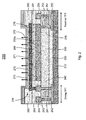
- Fig. 2 illustrates a cross-sectional view of a pixel structure 200 of an AMOLED display according to one embodiment of the invention.
- the pixel 200 of the AMOLED display includes at least structures as set forth below.
- a supporting substrate 210 has a first end portion corresponding to a driving TFT 240 and an opposite, second end portion corresponding to a read-out TFT 250.
- a semiconductor layer having a first portion 242 and a second portion 252 is correspondingly disposed on the first and second end portions of the substrate 210.
- a gate insulator layer 220 is formed on the substrate 210 and covers the semiconductor layer.
- a gate metal layer having a first portion 241 and a second portion 251 is correspondingly disposed on the two end portions of the gate insulator layer 220 via an interlayer dielectric (ILD) 230.
- ILD interlayer dielectric
- a first source metal layer 243 and a first drain metal layer 244 are electrically connected to the first portion 242 of the semiconductor layer and correspondingly disposed on the first end portion of the interlayer dielectric 230.
- a second source metal layer 253 and a second drain metal layer 254 are electrically connected to the second portion 252 of the semiconductor layer and correspondingly disposed on the second end portion of the interlayer dielectric 230.
- the first portion 241 of the gate metal layer, the first portion 242 of the semiconductor layer, the first source metal layer 243 and a first drain metal layer 244 constitute the driving TFT 240.
- the second portion 251 of the gate metal layer, the second portion 252 of the semiconductor layer, the second source metal layer 253 and a second drain metal layer 254 constitute the driving TFT 250.
- a photo sensor includes a photosensitive (Si-rich dielectric) layer 260 disposed on an extending portion 253a of the second source metal layer 253 extending to an emission region of the pixel 200 of the display.
- a first passivation layer 281 correspondingly disposed on the first and second end portions of the interlayer dielectric 230, so as to define a space therebetween in which the extending portion 253a of the second source metal layer 253 and the photosensitive layer 260 are deposed.
- a second passivation layer 282 correspondingly disposed on the first passivation layer 281.
- An OLED 270 has an anode layer 271 deposed on the photosensitive layer 260 and electrically connected to the first source metal layer 243 over the emission region of the pixel 200 of the display, an OLED emissive layer 272 disposed on and covered both the second passivation layer 282 and the anode layer 271, and a cathode layer 273 disposed on and covered the OLED emissive layer 272.
- the anode layer 271 of the OLED 270 is formed such that at least a portion that overlaps the photosensitive layer 260 of the photo sensor is partially transparent to light emitted from the emissive layer 272 of the OLED 270.
- the other portion of the anode layer 271 of the OLED 270 may or may not be transparent to light emitted from the emissive layer 272 of the OLED 270.
- the OLED 270 is a top emission OLED, i.e., the majority portion 275 of light emitted from the OLED emissive layer 272 transmits out from the cathode layer 273.
- the remaining portion 276 of the light emitted from the OLED emissive layer 272 transmits out from the anode layer 271 and to the photosensitive layer 260.
- the photo sensor measures the brightness of the remaining portion 276 of the light, i.e., an ambient light to the photo sensor, which is proportional to the light emitted from the OLED emissive layer 272, and generating a sensing signal corresponding to the measured brightness of the ambient light.
- the read-out TFT 250 reads and outputs the sensing signal.
- the sensing signal in turn, is utilized to adjust a driving voltage of the OLED 270 through the driving TFT 240 accordingly.
- Fig. 3 shows a pixel structure 300 of an AMOLED display according to another embodiment of the invention.
- the pixel structure 300 are similar to the pixel structure 200 disclosed above and shown in Fig. 2 , except that the OLED 370 is a bottom emission OLED, i.e., the light 375 emitted from the OLED emissive layer 372 transmits out from the anode layer 371.
- the anode layer 371 is formed to be transparent to light emitted from the emissive layer 372 of the OLED 370.
- the photosensitive layer 360 defines a photo sensing area that is much less than that corresponding to the top emission OLED shown in Fig. 2 .
- the photosensitive layer 360 is formed between the anode layer 371 of the OLED 370 and the second source layer 353 of the read-out TFT 350, as such the majority portion of the space defined between the diving TFT 340 and the read-out TFT 350 is corresponding to an emission region of the OLED 370.
- the majority portion of the light 375 emitted from the OLED emissive layer372 transmits out from the emission region, while the remaining portion of the light 375 transmits out from the anode layer 371 and to the photosensitive layer 360.
- the photo sensor measures the brightness of the remaining portion of the light 375, i.e., an ambient light to the photo sensor, which is proportional to the light 375 emitted from the OLED emissive layer 372, and generating a sensing signal corresponding to the measured brightness of the ambient light.
- the read-out TFT 350 reads and outputs the sensing signal.
- the sensing signal in turn, is utilized to adjust a driving voltage of the OLED 370 through the driving TFT 340 accordingly.
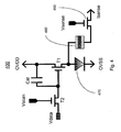
- Fig. 4 shows a circuit diagram of a pixel 400 of an AMOLED display according to yet another embodiment of the invention.
- the AMOLED display has an AMOLED panel having a plurality of pixels 400 arranged in an array.
- Each pixel 400 includes an OLED 470 having a cathode electrically coupled to a first supply voltage, OVSS, an anode and an emissive layer formed between the cathode and the anode.
- the OLED 470 can be a top-emitting OLED or a bottom-emitting OLED.
- Each pixel 400 also includes a first transistor T1 having a gate, a drain electrically coupled to a second supply voltage, OVDD, and a source electrically coupled to the anode of the OLED 470, a second transistor T2 having a gate electrically coupled to a scan signal, Vscan(N), a drain electrode electrically coupled to the gate of the first transistor T1, and a source electrode electrically coupled to a data signal, Vdata, and a storage capacitor Cst electrically connected between the gate and the drain of the first transistor T1.
- the first supply voltage OVSS and the second supply voltage OVDD are a negative supply voltage and a positive supply voltage, respectively.
- each pixel 400 includes a read-out TFT 450 having a gate electrically coupled to a sensing control voltage, Vsense, a drain for outputting a sensing signal, Isense, and a source, and a photo sensor 460 electrically coupled between the anode of the OLED 470 and the source of the read-out transistor 450.
- the photo sensor 460 is adapted for optical feedback compensation, specifically, for measuring brightness of an ambient light that is proportional to light emitted from the OLED 470 and generating the sensing signal Isense corresponding to the measured brightness of the ambient light.
- the sensing signal Isense in turn, is utilized to adjust the data signal Vdata.
- Each of the first transistor T1, the second transistor T2 and the read-out transistor 450 comprises an NMOS transistor or PMOS transistor.
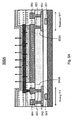
- Fig. 5 shows a pixel structure 500 of an AMOLED display according to one non-claimed embodiment.
- the display has a substrate 510, and a plurality of pixels 500 formed on the substrate 510 and arranged in an array.
- the pixel 500 includes a driving transistor 540 having a gate layer 541, a drain layer 544 and a source layer 543, formed on the substrate 510.
- the pixel 500 also includes an OLED 570 having a cathode layer 573, a anode layer 571 and an emissive layer 572 formed between the cathode layer 573 and the anode layer 571, and formed over the driving transistor 540 such that the anode layer 571 of the OLED 570 is electrically connected to the source layer 544 of the driving transistor 540.
- the pixel 500 includes a bias layer 550 formed over the substrate 510, and a photo sensor having a photosensitive layer 560 formed between the anode layer 571 of the OLED 570 and the bias layer 550.
- the driving TFT 540 is formed on one end portion of the supporting substrate 510.
- a semiconductor layer 542 is disposed on the one end portion of the substrate 510.
- a gate insulator layer 420 is disposed on the substrate 412 and covers the semiconductor layer 542.
- the gate metal layer 541 is disposed on the gate insulator layer 520 at a location that is over the semiconductor layer 542.
- An interlayer dielectric (ILD) layer 530 is deposed on the gate insulator layer 520 and covers the gate metal layer 541.
- the drain layer 544 and the source layer 543 of the driving TFT 540 are spatially formed on the interlayer dielectric layer 530 and are connected to the semiconductor layer 542.
- a metal bias electrode layer 550 is disposed on the interlayer dielectric layer 530 over the other end potion of the substrate 510 and extends into the emission region of the pixel 500.
- a photosensitive layer 560 is disposed on the metal bias electrode layer 550 at an emission region of the pixel 500.
- the anode layer 571 of the OLED 570 is disposed on the photosensitive layer 560 having one end portion electrically connected to the source layer 543 of the driving TFT 540, and the other end portion extended over the other end portion of the substrate 510.
- a first passivation layer 581 is correspondingly disposed on the two ends of the interlayer dielectric 530 so that the emission region of the pixel 500 is defined therebetween.
- a second passivation layer 582 is correspondingly disposed on the first passivation layer 581.
- the OLED emissive layer 572 of the OLED 570 is disposed on the anode layer 571 and covers both the second passivation layer 582 and the anode layer 571.
- the cathode layer 573 of the OLED 570 is disposed on and covers the OLED emissive layer 572 of the OLED 570.
- the OLED 570 is a top emission OLED, i.e., the majority portion 575 of light emitted from the OLED emissive layer 572 transmits out from the cathode layer 573.
- the remaining portion 576 of the light emitted from the OLED emissive layer 572 transmits out from the anode layer 573 and to the photosensitive layer 560.
- the photo sensor measures the brightness of the remaining portion 576 of the light, an ambient light to the photo sensor, which is proportional to the light emitted from the OLED emissive layer 572, and generating a sensing signal corresponding to the measured brightness of the ambient light.
- the read-out TFT 550 reads and outputs the sensing signal.
- the sensing signal is output from the bias electrode 560 and utilized to adjust a driving voltage of the OLED 570 through the driving TFT 540 accordingly.
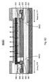
- Fig. 6 shows a pixel structure 600 of an AMOLED display according to another non-claimed embodiment.
- the pixel structure 600 are similar to the pixel structure 500 disclosed above and shown in Fig. 5 , except that the OLED 670 is a bottom emission OLED, i.e., the light 675 emitted from the OLED emissive layer 672 transmits out from the anode layer 671.
- the photosensitive layer 660 defines a photo sensing area that is much less than that corresponding to the top emission OLED shown in Fig. 5 .
- the photosensitive layer 660 is formed between the anode layer 671 of the OLED 670 and the bias electrode 650, as such the majority portion of the space defined between the diving TFT 640 and the bias electrode 650 is corresponding to an emission region of the OLED 670.
- the majority portion of the light 675 emitted from the OLED emissive layer 672 transmits out from the emission region, while the remaining portion of the light 675 transmits out from the anode layer 671 and to the photosensitive layer 660.
- the photo sensor measures the brightness of the remaining portion of the light 675, i.e., an ambient light to the photo sensor, which is proportional to the light 675 emitted from the OLED emissive layer 672, and generating a sensing signal corresponding to the measured brightness of the ambient light.
- the bias electrode 650 outputs the sensing signal.
- the sensing signal in turn, is utilized to adjust a driving voltage of the OLED 670 through the driving TFT 640 accordingly.
- Fig. 7 shows a circuit diagram of a pixel 700 of an AMOLED display according to yet another non-claimed embodiment.
- the AMOLED display has an AMOLED panel having a plurality of pixels 700 arranged in an array.
- Each pixel 700 includes an OLED 770 having a cathode electrically coupled to a first supply voltage, OVSS, an anode and an emissive layer formed between the cathode and the anode.
- the OLED 770 can be a top-emitting OLED or a bottom-emitting OLED.
- Each pixel 700 also includes a first transistor T1 having a gate, a drain electrically coupled to a second supply voltage, OVDD, and a source electrically coupled to the anode of the OLED 770, a second transistor T2 having a gate electrically coupled to a scan signal, Vscan(N), a drain electrode electrically coupled to the gate of the first transistor T1, and a source electrode electrically coupled to a data signal, Vdata, and a storage capacitor Cst electrically connected between the gate and the drain of the first transistor T1.
- the first supply voltage OVSS and the second supply voltage OVDD are a negative supply voltage and a positive supply voltage, respectively.
- Each of the first transistor T1 and the second transistor T2 comprises an NMOS transistor or PMOS transistor.
- each pixel 700 includes a photo sensor 760 electrically coupled to the anode of the OLED 770 for measuring brightness of an ambient light that is proportional to light emitted from the OLED 770 and generating the sensing signal I 2 corresponding to the measured brightness of the ambient light, and a bias electrode (line) 750 electrically coupled to the photo sensor 760 for outputting the sensing signal I 2 .
- the generated current of the OLED 770, I OLED (I 1 - I 2 ), where I 1 is the current flow from the drain to the source of the first TFT T1, and I 2 is the sensing current of the photo sensor 760 that is output from the bias line 750.
- the sensing current I 2 is adapted for optical feedback compensation.
- the photo sensor current I2 increases, which in turn, results in a decrease of the OLED current I OLED , so that the light of the OLED 770 become darker.
- the photo sensor current I2 decreases, which in turn, results in an increase of the OLED current I OLED , so that the light of the OLED 770 become brighter.
- the AMOLED display panel will not generate line mura during operation, largely improving the display quality of the AMOLED display panel.
- Figs. 8A-8D disclose a pixel structure of an AMOLED display according to four different embodiments 800A-800D of the invention. Each embodiment corresponds to a different type of the driving TFT and the read-out TFT. In these embodiments, each of the driving TFT and the read-out TFT is formed with a semiconductive layer 842/852, a gate layer841/851, a source layer 843/853 and a drain layer 844/854. Different fabrication processes produce different type TFTs.
- the driving TFT 840A and the read-out TFT 850A are respectively formed in a bottom gate type TFT.
- Fig. 8B shows the driving TFT 840B and the read-out TFT 850B respectively formed in a coplanar type TFT.
- Fig. 8C shows the driving TFT 840C and the read-out TFT 850C respectively formed in a back channel etched (BCE) type TFT.
- Fig. 8D shows the driving TFT 840D and the read-out TFT 850D respectively formed in an IS type TFT, where an etch stop layer 845/855 is deposed on the semiconductive layer 842/852.
- the supporting substrate which can include, but not limited to, glass, plastic, semiconductor materials, silicon, ceramics, and circuit board materials.
- the semiconductor layer can include, but not limited to, polysilicon, (coplanar/IS/BCE structure) metal oxide materials such as IZO, IGZO, AnO and In 2 O 3 .
- the gate insulator layer can include, but not limited to, SiOx, SiNx, SiOx/SiNx and AlOx.
- the gate metal layer can include, but not limited to, Mo, AlNd, Ti/AlTi, Mo/Al/Mo and Cu.
- the interlayer dielectric layer can include, but not limited to, SiOx, SiNx and SiOx/SiNx.
- the etch stop layer can include, but not limited to, SiOx, SiNx and AlOx.
- the source/drain metal layer can include, but not limited to, Mo, AINd, Ti/Al/Ti, Mo/AI/Mo and Cu.
- the metal bias line layer can include, but not limited to, Mo, AiNd, Ti/Al/Ti, Mo/AI/Mo and Cu.
- the photsenstive layer can include, but not limited to, Si-rch dielectric or other photosensitive materials.
- the anode layer can include, but not limited to, ITO, IZO, AI, Ag, AI/ITO, Ag/ITO, ITO/Ag/ITO and Mo/Al/ITO.
- the first passivation layer can include, but not limited to, SiOx, SiNx, SiOx/organic materials, SiNx/organic materials and organic materials.
- the second passivation layer can include, but not limited to, SiOX, SiNx and organice materials.
- One aspect of the present invention relates to a method of driving a display in accordance with claim 1 and having an active matrix organic light emitting diode (AMOLED) panel having a plurality of pixels arranged in an array, each pixel comprising an organic light emitting diode (OLED).
- the method includes the steps of measuring brightness of an ambient light that is proportional to light emitted from the OLED so as to generate a sensing signal corresponding to the measured brightness of the ambient light, and adjusting a driving voltage of the OLED according to the sensing signal.
- the measuring step is performed with a photo sensor coupled to the OLED.
- the present invention discloses an AMOLED display with each pixel incorporated with a photo sensor for optical feedback compensation so as to improve the performance of the AMOLED display.
Claims (4)
- Affichage d'écran comprenant :un panneau à diodes électroluminescentes organiques à matrice active (AMOLED) ayant une pluralité de pixels (400) disposés dans un réseau, chaque pixel (400) comprenant :(a) une diode électroluminescente organique (470) ayant une cathode couplée électriquement à une première tension d'alimentation (OVSS), une anode et une couche émettrice formée entre la cathode et l'anode ;(b) un circuit d'entraînement ayant :(i) un premier transistor (T1) ayant une grille, un drain couplé électriquement à une seconde tension d'alimentation (OVDD) et une source couplée électriquement à l'anode de la diode électroluminescente organique (470) ;(ii) un second transistor (T2) ayant une grille couplée électriquement à un signal de balayage (Vscan(N)), une électrode de drain couplée électriquement à la grille du premier transistor (T1), et une électrode de source couplée électriquement à un signal de données (Vdata) ; et(iii) un condensateur de puissance (Cst) raccordé électriquement entre la grille et le drain du premier transistor (T1) ;(c) un transistor de lecture (450) ayant une grille couplée électriquement à une tension de commande de détection (Vsense), un drain pour produire un signal de détection (Isense), et une source ; et(d) un photodétecteur (460)caractérisé par le fait que le photodétecteur (460) est couplé électriquement entre l'anode de la diode électroluminescente organique (450) et la source du transistor de lecture (450),dans lequel le photodétecteur (460) est adapté pour mesurer l'intensité d'une lumière ambiante qui est proportionnelle à la lumière émise par la diode électroluminescente organique (450) et pour générer un signal de détection (Vbias) correspondant à l'intensité mesurée de la lumière ambiante, dans lequel le signal de données (Vdata) est réglé en fonction du signal de détection (Vbias).
- Affichage d'écran selon la revendication 1, dans lequel la diode électroluminescente organique (470) comprend une DELo à émission par la surface supérieure ou une DELo à émission par la surface inférieure.
- Affichage d'écran selon la revendication 2, dans lequel la couche photosensible définit une zone photosensible, dans lequel la zone photosensible pour la DELo à émission par la surface supérieure est plus grande que pour la DELo à émission par la surface inférieure.
- Affichage d'écran selon la revendication 1, dans lequel chacun des transistors (T1, T2, 460) comprend un transistor NMOS ou un transistor PMOS.
Priority Applications (2)
| Application Number | Priority Date | Filing Date | Title |
|---|---|---|---|
| EP15180452.3A EP2998996B1 (fr) | 2010-03-11 | 2010-08-16 | Écran a diodes electroluminescentes organiques a matrice active a compensation optique de réaction |
| EP18193904.2A EP3499575A1 (fr) | 2010-03-11 | 2010-08-16 | Écran à diodes électroluminescentes organiques à matrice active à compensation optique de réaction |
Applications Claiming Priority (1)
| Application Number | Priority Date | Filing Date | Title |
|---|---|---|---|
| US12/722,040 US8669924B2 (en) | 2010-03-11 | 2010-03-11 | Amoled display with optical feedback compensation |
Related Child Applications (3)
| Application Number | Title | Priority Date | Filing Date |
|---|---|---|---|
| EP18193904.2A Division EP3499575A1 (fr) | 2010-03-11 | 2010-08-16 | Écran à diodes électroluminescentes organiques à matrice active à compensation optique de réaction |
| EP15180452.3A Division-Into EP2998996B1 (fr) | 2010-03-11 | 2010-08-16 | Écran a diodes electroluminescentes organiques a matrice active a compensation optique de réaction |
| EP15180452.3A Division EP2998996B1 (fr) | 2010-03-11 | 2010-08-16 | Écran a diodes electroluminescentes organiques a matrice active a compensation optique de réaction |
Publications (3)
| Publication Number | Publication Date |
|---|---|
| EP2365529A2 EP2365529A2 (fr) | 2011-09-14 |
| EP2365529A3 EP2365529A3 (fr) | 2012-08-01 |
| EP2365529B1 true EP2365529B1 (fr) | 2015-09-16 |
Family
ID=43431979
Family Applications (3)
| Application Number | Title | Priority Date | Filing Date |
|---|---|---|---|
| EP18193904.2A Withdrawn EP3499575A1 (fr) | 2010-03-11 | 2010-08-16 | Écran à diodes électroluminescentes organiques à matrice active à compensation optique de réaction |
| EP10172977.0A Active EP2365529B1 (fr) | 2010-03-11 | 2010-08-16 | Affichage d'écran AMOLED avec compensation optique de réaction |
| EP15180452.3A Active EP2998996B1 (fr) | 2010-03-11 | 2010-08-16 | Écran a diodes electroluminescentes organiques a matrice active a compensation optique de réaction |
Family Applications Before (1)
| Application Number | Title | Priority Date | Filing Date |
|---|---|---|---|
| EP18193904.2A Withdrawn EP3499575A1 (fr) | 2010-03-11 | 2010-08-16 | Écran à diodes électroluminescentes organiques à matrice active à compensation optique de réaction |
Family Applications After (1)
| Application Number | Title | Priority Date | Filing Date |
|---|---|---|---|
| EP15180452.3A Active EP2998996B1 (fr) | 2010-03-11 | 2010-08-16 | Écran a diodes electroluminescentes organiques a matrice active a compensation optique de réaction |
Country Status (4)
| Country | Link |
|---|---|
| US (2) | US8669924B2 (fr) |
| EP (3) | EP3499575A1 (fr) |
| CN (1) | CN101976679B (fr) |
| TW (1) | TWI496279B (fr) |
Families Citing this family (62)
| Publication number | Priority date | Publication date | Assignee | Title |
|---|---|---|---|---|
| US9183779B2 (en) * | 2012-02-23 | 2015-11-10 | Broadcom Corporation | AMOLED light sensing |
| TWI480998B (zh) * | 2012-05-24 | 2015-04-11 | Au Optronics Corp | 有機發光畫素的結構、製作方法以及驅動電路 |
| CN102664187B (zh) * | 2012-05-29 | 2016-01-20 | 南京中电熊猫液晶显示科技有限公司 | 有机发光二极管显示器及其制造方法 |
| CN102760755B (zh) * | 2012-07-27 | 2015-07-15 | 南京中电熊猫液晶显示科技有限公司 | 一种金属氧化物有机发光二极管显示装置及其制造方法 |
| US9019253B2 (en) | 2012-08-30 | 2015-04-28 | Apple Inc. | Methods and systems for adjusting color gamut in response to ambient conditions |
| US9666119B2 (en) | 2012-08-30 | 2017-05-30 | Apple Inc. | Systems and methods for controlling current in display devices |
| KR20140064328A (ko) | 2012-11-20 | 2014-05-28 | 엘지디스플레이 주식회사 | 유기전계 발광소자 및 이의 제조 방법 |
| US8952947B2 (en) * | 2012-12-07 | 2015-02-10 | Htc Corporation | Display method for sunlight readable and electronic device using the same |
| US9111757B2 (en) | 2013-04-25 | 2015-08-18 | Apple Inc. | Display having a backplane with interlaced laser crystallized regions |
| TWI486839B (zh) * | 2013-06-03 | 2015-06-01 | Ye Xin Technology Consulting Co Ltd | 觸控顯示裝置 |
| TWI516028B (zh) * | 2013-06-20 | 2016-01-01 | 財團法人工業技術研究院 | 高低壓隔離內埋功率模組 |
| EP2860720A1 (fr) * | 2013-10-10 | 2015-04-15 | Nederlandse Organisatie voor toegepast- natuurwetenschappelijk onderzoek TNO | Unité électro-optique, dispositif électro-optique et procédé de fonctionnement d'un dispositif électro-optique |
| KR102116896B1 (ko) | 2013-10-14 | 2020-06-01 | 삼성디스플레이 주식회사 | 유기 발광 표시 장치 |
| KR20150043136A (ko) | 2013-10-14 | 2015-04-22 | 삼성디스플레이 주식회사 | 유기 발광 표시 장치 및 이의 제조 방법 |
| KR102207563B1 (ko) | 2013-10-29 | 2021-01-27 | 삼성디스플레이 주식회사 | 유기 발광 표시장치 및 유기 발광 표시장치의 제조 방법 |
| KR102144084B1 (ko) | 2013-11-19 | 2020-08-14 | 삼성디스플레이 주식회사 | 터치 스크린 패널 일체형 표시장치 |
| CN103646629B (zh) * | 2013-12-18 | 2016-06-08 | 信利半导体有限公司 | 一种主动矩阵有机发光显示器的像素驱动装置 |
| CN103956142B (zh) * | 2014-05-15 | 2016-03-09 | 深圳市华星光电技术有限公司 | 面板驱动电路及面板驱动方法 |
| CN104157237B (zh) | 2014-07-18 | 2016-05-11 | 京东方科技集团股份有限公司 | 一种显示驱动电路及其驱动方法、显示装置 |
| CN105468205B (zh) * | 2014-09-03 | 2018-08-31 | 上海和辉光电有限公司 | 整合于amoled面板中的触控装置及其制备方法 |
| KR102553156B1 (ko) * | 2014-12-29 | 2023-07-06 | 엘지디스플레이 주식회사 | 유기발광표시장치 및 이의 동작방법 |
| TWI563489B (en) | 2015-02-24 | 2016-12-21 | Au Optronics Corp | Display and operation method thereof |
| CN104966718B (zh) * | 2015-05-04 | 2017-12-29 | 深圳市华星光电技术有限公司 | Amoled背板的制作方法及其结构 |
| CN105185351B (zh) * | 2015-10-13 | 2017-07-28 | 深圳市华星光电技术有限公司 | 提升oled显示面板对比度的方法及系统 |
| CN105633171A (zh) | 2016-03-22 | 2016-06-01 | 京东方科技集团股份有限公司 | 一种薄膜晶体管及其制作方法、显示装置 |
| TWI569249B (zh) * | 2016-07-01 | 2017-02-01 | 友達光電股份有限公司 | 畫素電路 |
| CN107390406B (zh) * | 2017-06-20 | 2019-06-18 | 惠科股份有限公司 | 一种显示面板、显示面板的制造方法和显示装置 |
| CN107591425B (zh) * | 2017-08-23 | 2020-02-14 | 深圳市华星光电半导体显示技术有限公司 | Amoled显示面板以及显示装置 |
| CN107644892B (zh) * | 2017-09-15 | 2020-04-14 | 京东方科技集团股份有限公司 | 一种oled光源、显示装置及制备方法 |
| WO2019075746A1 (fr) * | 2017-10-20 | 2019-04-25 | 深圳市柔宇科技有限公司 | Capteur de lumière et écran d'affichage à diodes électroluminescentes organiques |
| US11327383B2 (en) * | 2017-12-07 | 2022-05-10 | Boe Technology Group Co., Ltd. | Display panel with light transmittance controlled by gate line and data line |
| CN108493214A (zh) * | 2018-03-15 | 2018-09-04 | 业成科技(成都)有限公司 | 有机发光二极体显示器及其光学补偿方法 |
| CN110164370B (zh) * | 2018-05-14 | 2021-08-10 | 京东方科技集团股份有限公司 | 一种像素电路、补偿组件、显示装置及其驱动方法 |
| CN108831912B (zh) | 2018-06-15 | 2020-11-24 | 京东方科技集团股份有限公司 | Oled阵列基板及制造其的方法、oled像素电路以及显示装置 |
| CN108807495B (zh) * | 2018-07-20 | 2021-01-26 | 京东方科技集团股份有限公司 | 阵列基板、显示面板及其测光方法和控制方法 |
| CN108922918B (zh) * | 2018-09-10 | 2021-01-26 | 京东方科技集团股份有限公司 | 一种oled显示面板及其制作方法、oled显示装置 |
| KR102554283B1 (ko) * | 2018-10-30 | 2023-07-10 | 엘지디스플레이 주식회사 | 표시장치 |
| CN109147663A (zh) * | 2018-11-28 | 2019-01-04 | 南京中电熊猫平板显示科技有限公司 | 一种有机发光显示装置及其亮度补偿方法 |
| CN109728050A (zh) | 2019-01-02 | 2019-05-07 | 京东方科技集团股份有限公司 | 一种阵列基板及其制备方法、显示面板和显示装置 |
| CN109728060B (zh) * | 2019-01-04 | 2021-02-02 | 京东方科技集团股份有限公司 | 一种阵列基板、电致发光面板及显示装置 |
| CN109742126B (zh) * | 2019-01-11 | 2022-02-11 | 京东方科技集团股份有限公司 | 显示基板及其制备方法、显示面板、显示装置 |
| US11232750B2 (en) | 2019-01-29 | 2022-01-25 | Boe Technology Group Co., Ltd. | Display substrate, display panel, and manufacturing method and driving method of display substrate |
| US11740723B2 (en) | 2019-05-02 | 2023-08-29 | Apple Inc. | Electronic devices having light sensors overlapped by displays |
| CN110197842B (zh) * | 2019-05-30 | 2022-09-27 | 京东方科技集团股份有限公司 | Oled底发射结构及其驱动方法 |
| CN110164946B (zh) * | 2019-06-06 | 2022-04-29 | 京东方科技集团股份有限公司 | 显示基板及制造方法、显示装置 |
| CN110245610A (zh) * | 2019-06-14 | 2019-09-17 | 京东方科技集团股份有限公司 | 显示背板及其制作方法和全面屏指纹识别显示装置 |
| CN110428766A (zh) * | 2019-06-27 | 2019-11-08 | 福建华佳彩有限公司 | 不规则屏均匀显示方法及均匀显示的不规则屏 |
| CN110536082B (zh) * | 2019-08-30 | 2021-11-02 | 上海中航光电子有限公司 | 主动式像素传感电路及传感器、显示面板及装置 |
| CN110634929B (zh) * | 2019-09-26 | 2022-02-08 | 京东方科技集团股份有限公司 | 显示基板及其制备方法、亮度补偿方法、显示装置 |
| US10796639B1 (en) * | 2019-09-27 | 2020-10-06 | Int Tech Co., Ltd. | Display device and method for calibrating the same |
| CN110689831A (zh) * | 2019-11-07 | 2020-01-14 | 京东方科技集团股份有限公司 | 显示面板、其亮度补偿方法及显示装置 |
| CN110867473B (zh) * | 2019-11-26 | 2022-09-30 | 京东方科技集团股份有限公司 | 显示基板、显示面板及显示装置 |
| CN113366563B (zh) * | 2019-11-29 | 2022-08-09 | 京东方科技集团股份有限公司 | 显示基板及其制作方法、显示装置 |
| CN111293154A (zh) * | 2020-02-21 | 2020-06-16 | 武汉华星光电半导体显示技术有限公司 | 显示面板及显示装置 |
| CN111540775B (zh) | 2020-05-11 | 2023-07-18 | 京东方科技集团股份有限公司 | 显示基板及其制备方法和亮度补偿方法、显示装置 |
| CN111951732B (zh) * | 2020-08-21 | 2021-12-17 | 京东方科技集团股份有限公司 | 像素电路、显示面板及显示装置 |
| TWI770750B (zh) * | 2020-12-31 | 2022-07-11 | 友達光電股份有限公司 | 畫素陣列基板 |
| CN113990900B (zh) * | 2021-10-12 | 2023-05-30 | 武汉华星光电半导体显示技术有限公司 | 显示面板和移动终端 |
| CN114005405A (zh) * | 2021-10-19 | 2022-02-01 | 惠州华星光电显示有限公司 | 显示面板及其亮度补偿方法 |
| US20230122765A1 (en) * | 2021-10-19 | 2023-04-20 | Huizhou China Star Optoelectronics Display Co., Ltd. | Display panel and brightness compensation method thereof |
| CN114420051B (zh) * | 2022-01-28 | 2023-08-22 | 京东方科技集团股份有限公司 | 一种人机交互像素电路及oled显示屏 |
| CN114566126B (zh) * | 2022-03-10 | 2023-08-22 | 武汉华星光电半导体显示技术有限公司 | 显示面板 |
Family Cites Families (21)
| Publication number | Priority date | Publication date | Assignee | Title |
|---|---|---|---|---|
| WO2001020591A1 (fr) * | 1999-09-11 | 2001-03-22 | Koninklijke Philips Electronics N.V. | Dispositif d'affichage electroluminescent a matrice active |
| TW480727B (en) | 2000-01-11 | 2002-03-21 | Semiconductor Energy Laboratro | Semiconductor display device |
| US6774578B2 (en) * | 2000-09-19 | 2004-08-10 | Semiconductor Energy Laboratory Co., Ltd. | Self light emitting device and method of driving thereof |
| JP2002162934A (ja) * | 2000-09-29 | 2002-06-07 | Eastman Kodak Co | 発光フィードバックのフラットパネルディスプレイ |
| JP2002278504A (ja) | 2001-03-19 | 2002-09-27 | Mitsubishi Electric Corp | 自発光型表示装置 |
| US20040031966A1 (en) | 2002-08-16 | 2004-02-19 | Forrest Stephen R. | Organic photonic integrated circuit using a photodetector and a transparent organic light emitting device |
| GB0307789D0 (en) * | 2003-04-04 | 2003-05-07 | Koninkl Philips Electronics Nv | Electroluminescent display devices |
| US7053412B2 (en) * | 2003-06-27 | 2006-05-30 | The Trustees Of Princeton University And Universal Display Corporation | Grey scale bistable display |
| US20060007248A1 (en) * | 2004-06-29 | 2006-01-12 | Damoder Reddy | Feedback control system and method for operating a high-performance stabilized active-matrix emissive display |
| US20050200291A1 (en) * | 2004-02-24 | 2005-09-15 | Naugler W. E.Jr. | Method and device for reading display pixel emission and ambient luminance levels |
| EP1730781A1 (fr) * | 2004-03-24 | 2006-12-13 | Koninklijke Philips Electronics N.V. | Dispositifs d'affichage electroluminescents |
| GB0406540D0 (en) | 2004-03-24 | 2004-04-28 | Koninkl Philips Electronics Nv | Electroluminescent display devices |
| KR100621561B1 (ko) | 2004-11-05 | 2006-09-19 | 삼성전자주식회사 | Cmos 이미지 센서 및 그 구동 방법 |
| US20060180890A1 (en) * | 2005-01-18 | 2006-08-17 | Naugler W E Jr | Top emission flat panel display with sensor feedback stabilization |
| JP2006253316A (ja) * | 2005-03-09 | 2006-09-21 | Sony Corp | 固体撮像装置 |
| US7449697B2 (en) * | 2006-01-04 | 2008-11-11 | Tpo Displays Corp. | Organic electroluminescent devices and fabrication methods thereof |
| KR20070083352A (ko) * | 2006-02-21 | 2007-08-24 | 삼성전자주식회사 | 표시 장치 및 그 구동 방법 |
| EP1837912A1 (fr) * | 2006-03-22 | 2007-09-26 | Toppoly Optoelectronics Corp. | Dispositif électroluminescent organique et méthode de fabrication |
| US7397065B2 (en) | 2006-05-02 | 2008-07-08 | Tpo Displays Corp. | Organic electroluminescent device and fabrication methods thereof |
| KR100762682B1 (ko) * | 2006-05-03 | 2007-10-01 | 삼성에스디아이 주식회사 | 유기 전계 발광표시장치 및 그의 제조방법 |
| TWI333275B (en) | 2008-05-09 | 2010-11-11 | Au Optronics Corp | Method for fabricating light sensor |
-
2010
- 2010-03-11 US US12/722,040 patent/US8669924B2/en active Active
- 2010-08-13 TW TW099127191A patent/TWI496279B/zh active
- 2010-08-16 EP EP18193904.2A patent/EP3499575A1/fr not_active Withdrawn
- 2010-08-16 EP EP10172977.0A patent/EP2365529B1/fr active Active
- 2010-08-16 EP EP15180452.3A patent/EP2998996B1/fr active Active
- 2010-09-06 CN CN2010102763023A patent/CN101976679B/zh active Active
-
2014
- 2014-01-13 US US14/153,881 patent/US9007353B2/en active Active
Also Published As
| Publication number | Publication date |
|---|---|
| TWI496279B (zh) | 2015-08-11 |
| EP2365529A3 (fr) | 2012-08-01 |
| CN101976679B (zh) | 2012-06-27 |
| US20110221720A1 (en) | 2011-09-15 |
| US20140125643A1 (en) | 2014-05-08 |
| EP3499575A1 (fr) | 2019-06-19 |
| EP2998996A2 (fr) | 2016-03-23 |
| EP2998996A3 (fr) | 2016-04-06 |
| TW201131752A (en) | 2011-09-16 |
| US8669924B2 (en) | 2014-03-11 |
| EP2365529A2 (fr) | 2011-09-14 |
| EP2998996B1 (fr) | 2018-11-07 |
| US9007353B2 (en) | 2015-04-14 |
| CN101976679A (zh) | 2011-02-16 |
Similar Documents
| Publication | Publication Date | Title |
|---|---|---|
| EP2365529B1 (fr) | Affichage d'écran AMOLED avec compensation optique de réaction | |
| US9978313B2 (en) | Organic light emitting diode display, driving method thereof, and manufacturing method thereof | |
| US6762564B2 (en) | Display apparatus | |
| US8842058B2 (en) | Organic light emitting display | |
| KR100941836B1 (ko) | 유기 전계 발광표시장치 | |
| US7688292B2 (en) | Organic light emitting diode display device and driving method thereof | |
| KR100906964B1 (ko) | 유기 전계발광 구동 소자와 이를 갖는 유기 전계발광 표시패널 | |
| US10651256B2 (en) | Thin film transistor substrate for organic light-emitting diode display and manufacturing method thereof | |
| US20160190220A1 (en) | Manufacture method of amoled back plate and sturcture thereof | |
| US10950822B2 (en) | Display device capable of improving light extraction efficiency | |
| KR102268493B1 (ko) | 유기발광다이오드 표시장치 및 이의 제조방법 | |
| WO2020113857A1 (fr) | Dispositif à diodes électroluminescentes organiques flexible et son procédé de formation | |
| KR20120090190A (ko) | 유기발광다이오드 표시장치 및 그 제조 방법 | |
| US20110057181A1 (en) | Organic light emitting diode display | |
| KR20190107256A (ko) | 유기 발광 표시 장치 | |
| KR20210014817A (ko) | 표시 장치 및 그의 제조 방법 | |
| KR100482328B1 (ko) | 액티브 매트릭스형 유기 전계발광 표시패널 및 그의제조방법 | |
| US20200043953A1 (en) | Array substrate and display device | |
| KR102273542B1 (ko) | 표시장치 | |
| KR101267077B1 (ko) | 유기 전계 발광 표시소자 및 그 제조방법 | |
| KR20200077322A (ko) | 표시장치 | |
| KR20050068232A (ko) | 액티브 매트릭스형 유기전계발광 소자 및 그 제조방법 |
Legal Events
| Date | Code | Title | Description |
|---|---|---|---|
| PUAI | Public reference made under article 153(3) epc to a published international application that has entered the european phase |
Free format text: ORIGINAL CODE: 0009012 |
|
| 17P | Request for examination filed |
Effective date: 20100916 |
|
| AK | Designated contracting states |
Kind code of ref document: A2 Designated state(s): AL AT BE BG CH CY CZ DE DK EE ES FI FR GB GR HR HU IE IS IT LI LT LU LV MC MK MT NL NO PL PT RO SE SI SK SM TR |
|
| AX | Request for extension of the european patent |
Extension state: BA ME RS |
|
| PUAL | Search report despatched |
Free format text: ORIGINAL CODE: 0009013 |
|
| AK | Designated contracting states |
Kind code of ref document: A3 Designated state(s): AL AT BE BG CH CY CZ DE DK EE ES FI FR GB GR HR HU IE IS IT LI LT LU LV MC MK MT NL NO PL PT RO SE SI SK SM TR |
|
| AX | Request for extension of the european patent |
Extension state: BA ME RS |
|
| RIC1 | Information provided on ipc code assigned before grant |
Ipc: H01L 27/32 20060101AFI20120628BHEP |
|
| RIC1 | Information provided on ipc code assigned before grant |
Ipc: H01L 27/32 20060101AFI20150210BHEP Ipc: G09G 5/10 20060101ALI20150210BHEP Ipc: G09G 3/32 20060101ALI20150210BHEP |
|
| GRAP | Despatch of communication of intention to grant a patent |
Free format text: ORIGINAL CODE: EPIDOSNIGR1 |
|
| INTG | Intention to grant announced |
Effective date: 20150409 |
|
| GRAS | Grant fee paid |
Free format text: ORIGINAL CODE: EPIDOSNIGR3 |
|
| GRAA | (expected) grant |
Free format text: ORIGINAL CODE: 0009210 |
|
| AK | Designated contracting states |
Kind code of ref document: B1 Designated state(s): AL AT BE BG CH CY CZ DE DK EE ES FI FR GB GR HR HU IE IS IT LI LT LU LV MC MK MT NL NO PL PT RO SE SI SK SM TR |
|
| REG | Reference to a national code |
Ref country code: GB Ref legal event code: FG4D |
|
| REG | Reference to a national code |
Ref country code: CH Ref legal event code: EP |
|
| REG | Reference to a national code |
Ref country code: IE Ref legal event code: FG4D |
|
| REG | Reference to a national code |
Ref country code: AT Ref legal event code: REF Ref document number: 750400 Country of ref document: AT Kind code of ref document: T Effective date: 20151015 |
|
| REG | Reference to a national code |
Ref country code: DE Ref legal event code: R096 Ref document number: 602010027519 Country of ref document: DE |
|
| REG | Reference to a national code |
Ref country code: NL Ref legal event code: MP Effective date: 20150916 |
|
| PG25 | Lapsed in a contracting state [announced via postgrant information from national office to epo] |
Ref country code: FI Free format text: LAPSE BECAUSE OF FAILURE TO SUBMIT A TRANSLATION OF THE DESCRIPTION OR TO PAY THE FEE WITHIN THE PRESCRIBED TIME-LIMIT Effective date: 20150916 Ref country code: GR Free format text: LAPSE BECAUSE OF FAILURE TO SUBMIT A TRANSLATION OF THE DESCRIPTION OR TO PAY THE FEE WITHIN THE PRESCRIBED TIME-LIMIT Effective date: 20151217 Ref country code: LT Free format text: LAPSE BECAUSE OF FAILURE TO SUBMIT A TRANSLATION OF THE DESCRIPTION OR TO PAY THE FEE WITHIN THE PRESCRIBED TIME-LIMIT Effective date: 20150916 Ref country code: NO Free format text: LAPSE BECAUSE OF FAILURE TO SUBMIT A TRANSLATION OF THE DESCRIPTION OR TO PAY THE FEE WITHIN THE PRESCRIBED TIME-LIMIT Effective date: 20151216 Ref country code: LV Free format text: LAPSE BECAUSE OF FAILURE TO SUBMIT A TRANSLATION OF THE DESCRIPTION OR TO PAY THE FEE WITHIN THE PRESCRIBED TIME-LIMIT Effective date: 20150916 |
|
| REG | Reference to a national code |
Ref country code: LT Ref legal event code: MG4D |
|
| REG | Reference to a national code |
Ref country code: AT Ref legal event code: MK05 Ref document number: 750400 Country of ref document: AT Kind code of ref document: T Effective date: 20150916 |
|
| PG25 | Lapsed in a contracting state [announced via postgrant information from national office to epo] |
Ref country code: HR Free format text: LAPSE BECAUSE OF FAILURE TO SUBMIT A TRANSLATION OF THE DESCRIPTION OR TO PAY THE FEE WITHIN THE PRESCRIBED TIME-LIMIT Effective date: 20150916 Ref country code: SE Free format text: LAPSE BECAUSE OF FAILURE TO SUBMIT A TRANSLATION OF THE DESCRIPTION OR TO PAY THE FEE WITHIN THE PRESCRIBED TIME-LIMIT Effective date: 20150916 |
|
| PG25 | Lapsed in a contracting state [announced via postgrant information from national office to epo] |
Ref country code: NL Free format text: LAPSE BECAUSE OF FAILURE TO SUBMIT A TRANSLATION OF THE DESCRIPTION OR TO PAY THE FEE WITHIN THE PRESCRIBED TIME-LIMIT Effective date: 20150916 |
|
| PG25 | Lapsed in a contracting state [announced via postgrant information from national office to epo] |
Ref country code: ES Free format text: LAPSE BECAUSE OF FAILURE TO SUBMIT A TRANSLATION OF THE DESCRIPTION OR TO PAY THE FEE WITHIN THE PRESCRIBED TIME-LIMIT Effective date: 20150916 Ref country code: IT Free format text: LAPSE BECAUSE OF FAILURE TO SUBMIT A TRANSLATION OF THE DESCRIPTION OR TO PAY THE FEE WITHIN THE PRESCRIBED TIME-LIMIT Effective date: 20150916 Ref country code: CZ Free format text: LAPSE BECAUSE OF FAILURE TO SUBMIT A TRANSLATION OF THE DESCRIPTION OR TO PAY THE FEE WITHIN THE PRESCRIBED TIME-LIMIT Effective date: 20150916 Ref country code: EE Free format text: LAPSE BECAUSE OF FAILURE TO SUBMIT A TRANSLATION OF THE DESCRIPTION OR TO PAY THE FEE WITHIN THE PRESCRIBED TIME-LIMIT Effective date: 20150916 Ref country code: SK Free format text: LAPSE BECAUSE OF FAILURE TO SUBMIT A TRANSLATION OF THE DESCRIPTION OR TO PAY THE FEE WITHIN THE PRESCRIBED TIME-LIMIT Effective date: 20150916 Ref country code: IS Free format text: LAPSE BECAUSE OF FAILURE TO SUBMIT A TRANSLATION OF THE DESCRIPTION OR TO PAY THE FEE WITHIN THE PRESCRIBED TIME-LIMIT Effective date: 20160116 |
|
| PG25 | Lapsed in a contracting state [announced via postgrant information from national office to epo] |
Ref country code: PT Free format text: LAPSE BECAUSE OF FAILURE TO SUBMIT A TRANSLATION OF THE DESCRIPTION OR TO PAY THE FEE WITHIN THE PRESCRIBED TIME-LIMIT Effective date: 20160118 Ref country code: RO Free format text: LAPSE BECAUSE OF FAILURE TO SUBMIT A TRANSLATION OF THE DESCRIPTION OR TO PAY THE FEE WITHIN THE PRESCRIBED TIME-LIMIT Effective date: 20150916 Ref country code: AT Free format text: LAPSE BECAUSE OF FAILURE TO SUBMIT A TRANSLATION OF THE DESCRIPTION OR TO PAY THE FEE WITHIN THE PRESCRIBED TIME-LIMIT Effective date: 20150916 Ref country code: PL Free format text: LAPSE BECAUSE OF FAILURE TO SUBMIT A TRANSLATION OF THE DESCRIPTION OR TO PAY THE FEE WITHIN THE PRESCRIBED TIME-LIMIT Effective date: 20150916 |
|
| REG | Reference to a national code |
Ref country code: DE Ref legal event code: R097 Ref document number: 602010027519 Country of ref document: DE |
|
| REG | Reference to a national code |
Ref country code: FR Ref legal event code: PLFP Year of fee payment: 7 |
|
| PLBE | No opposition filed within time limit |
Free format text: ORIGINAL CODE: 0009261 |
|
| STAA | Information on the status of an ep patent application or granted ep patent |
Free format text: STATUS: NO OPPOSITION FILED WITHIN TIME LIMIT |
|
| 26N | No opposition filed |
Effective date: 20160617 |
|
| PG25 | Lapsed in a contracting state [announced via postgrant information from national office to epo] |
Ref country code: DK Free format text: LAPSE BECAUSE OF FAILURE TO SUBMIT A TRANSLATION OF THE DESCRIPTION OR TO PAY THE FEE WITHIN THE PRESCRIBED TIME-LIMIT Effective date: 20150916 |
|
| PG25 | Lapsed in a contracting state [announced via postgrant information from national office to epo] |
Ref country code: SI Free format text: LAPSE BECAUSE OF FAILURE TO SUBMIT A TRANSLATION OF THE DESCRIPTION OR TO PAY THE FEE WITHIN THE PRESCRIBED TIME-LIMIT Effective date: 20150916 |
|
| PG25 | Lapsed in a contracting state [announced via postgrant information from national office to epo] |
Ref country code: BE Free format text: LAPSE BECAUSE OF FAILURE TO SUBMIT A TRANSLATION OF THE DESCRIPTION OR TO PAY THE FEE WITHIN THE PRESCRIBED TIME-LIMIT Effective date: 20150916 |
|
| PG25 | Lapsed in a contracting state [announced via postgrant information from national office to epo] |
Ref country code: MC Free format text: LAPSE BECAUSE OF FAILURE TO SUBMIT A TRANSLATION OF THE DESCRIPTION OR TO PAY THE FEE WITHIN THE PRESCRIBED TIME-LIMIT Effective date: 20150916 |
|
| REG | Reference to a national code |
Ref country code: CH Ref legal event code: PL |
|
| PG25 | Lapsed in a contracting state [announced via postgrant information from national office to epo] |
Ref country code: LI Free format text: LAPSE BECAUSE OF NON-PAYMENT OF DUE FEES Effective date: 20160831 Ref country code: CH Free format text: LAPSE BECAUSE OF NON-PAYMENT OF DUE FEES Effective date: 20160831 |
|
| REG | Reference to a national code |
Ref country code: IE Ref legal event code: MM4A |
|
| REG | Reference to a national code |
Ref country code: FR Ref legal event code: PLFP Year of fee payment: 8 |
|
| PG25 | Lapsed in a contracting state [announced via postgrant information from national office to epo] |
Ref country code: IE Free format text: LAPSE BECAUSE OF NON-PAYMENT OF DUE FEES Effective date: 20160816 |
|
| PG25 | Lapsed in a contracting state [announced via postgrant information from national office to epo] |
Ref country code: LU Free format text: LAPSE BECAUSE OF NON-PAYMENT OF DUE FEES Effective date: 20160816 |
|
| PG25 | Lapsed in a contracting state [announced via postgrant information from national office to epo] |
Ref country code: HU Free format text: LAPSE BECAUSE OF FAILURE TO SUBMIT A TRANSLATION OF THE DESCRIPTION OR TO PAY THE FEE WITHIN THE PRESCRIBED TIME-LIMIT; INVALID AB INITIO Effective date: 20100816 Ref country code: SM Free format text: LAPSE BECAUSE OF FAILURE TO SUBMIT A TRANSLATION OF THE DESCRIPTION OR TO PAY THE FEE WITHIN THE PRESCRIBED TIME-LIMIT Effective date: 20150916 Ref country code: CY Free format text: LAPSE BECAUSE OF FAILURE TO SUBMIT A TRANSLATION OF THE DESCRIPTION OR TO PAY THE FEE WITHIN THE PRESCRIBED TIME-LIMIT Effective date: 20150916 |
|
| PG25 | Lapsed in a contracting state [announced via postgrant information from national office to epo] |
Ref country code: MK Free format text: LAPSE BECAUSE OF FAILURE TO SUBMIT A TRANSLATION OF THE DESCRIPTION OR TO PAY THE FEE WITHIN THE PRESCRIBED TIME-LIMIT Effective date: 20150916 Ref country code: MT Free format text: LAPSE BECAUSE OF NON-PAYMENT OF DUE FEES Effective date: 20160831 Ref country code: TR Free format text: LAPSE BECAUSE OF FAILURE TO SUBMIT A TRANSLATION OF THE DESCRIPTION OR TO PAY THE FEE WITHIN THE PRESCRIBED TIME-LIMIT Effective date: 20150916 |
|
| REG | Reference to a national code |
Ref country code: FR Ref legal event code: PLFP Year of fee payment: 9 |
|
| PG25 | Lapsed in a contracting state [announced via postgrant information from national office to epo] |
Ref country code: BG Free format text: LAPSE BECAUSE OF FAILURE TO SUBMIT A TRANSLATION OF THE DESCRIPTION OR TO PAY THE FEE WITHIN THE PRESCRIBED TIME-LIMIT Effective date: 20150916 |
|
| PG25 | Lapsed in a contracting state [announced via postgrant information from national office to epo] |
Ref country code: AL Free format text: LAPSE BECAUSE OF FAILURE TO SUBMIT A TRANSLATION OF THE DESCRIPTION OR TO PAY THE FEE WITHIN THE PRESCRIBED TIME-LIMIT Effective date: 20150916 |
|
| REG | Reference to a national code |
Ref country code: DE Ref legal event code: R079 Ref document number: 602010027519 Country of ref document: DE Free format text: PREVIOUS MAIN CLASS: H01L0027320000 Ipc: H10K0059000000 |
|
| P01 | Opt-out of the competence of the unified patent court (upc) registered |
Effective date: 20230516 |
|
| REG | Reference to a national code |
Ref country code: DE Ref legal event code: R081 Ref document number: 602010027519 Country of ref document: DE Owner name: AUO CORPORATION, TW Free format text: FORMER OWNER: AU OPTRONICS CORP., HSINCHU, TW Ref country code: DE Ref legal event code: R081 Ref document number: 602010027519 Country of ref document: DE Owner name: OPTRONIC SCIENCES LLC, ALLEN, US Free format text: FORMER OWNER: AU OPTRONICS CORP., HSINCHU, TW |
|
| PGFP | Annual fee paid to national office [announced via postgrant information from national office to epo] |
Ref country code: GB Payment date: 20230822 Year of fee payment: 14 |
|
| PGFP | Annual fee paid to national office [announced via postgrant information from national office to epo] |
Ref country code: FR Payment date: 20230824 Year of fee payment: 14 Ref country code: DE Payment date: 20230821 Year of fee payment: 14 |
|
| REG | Reference to a national code |
Ref country code: GB Ref legal event code: 732E Free format text: REGISTERED BETWEEN 20231109 AND 20231115 |
|
| REG | Reference to a national code |
Ref country code: DE Ref legal event code: R082 Ref document number: 602010027519 Country of ref document: DE Representative=s name: KELLER SCHNEIDER PATENTANWALTS GMBH, DE Ref country code: DE Ref legal event code: R081 Ref document number: 602010027519 Country of ref document: DE Owner name: OPTRONIC SCIENCES LLC, ALLEN, US Free format text: FORMER OWNER: AUO CORPORATION, HSINCHU, TW |