EP2365529B1 - AMOLED display with optical feedback compensation - Google Patents
AMOLED display with optical feedback compensation Download PDFInfo
- Publication number
- EP2365529B1 EP2365529B1 EP10172977.0A EP10172977A EP2365529B1 EP 2365529 B1 EP2365529 B1 EP 2365529B1 EP 10172977 A EP10172977 A EP 10172977A EP 2365529 B1 EP2365529 B1 EP 2365529B1
- Authority
- EP
- European Patent Office
- Prior art keywords
- oled
- layer
- transistor
- electrically coupled
- gate
- Prior art date
- Legal status (The legal status is an assumption and is not a legal conclusion. Google has not performed a legal analysis and makes no representation as to the accuracy of the status listed.)
- Active
Links
- 229920001621 AMOLED Polymers 0.000 title claims description 43
- 230000003287 optical effect Effects 0.000 title description 8
- 239000003990 capacitor Substances 0.000 claims description 3
- 239000010410 layer Substances 0.000 description 138
- 239000002184 metal Substances 0.000 description 21
- 229910052751 metal Inorganic materials 0.000 description 21
- 239000004065 semiconductor Substances 0.000 description 13
- 239000000758 substrate Substances 0.000 description 13
- 238000002161 passivation Methods 0.000 description 10
- 239000011229 interlayer Substances 0.000 description 9
- 229910004205 SiNX Inorganic materials 0.000 description 8
- 229910052814 silicon oxide Inorganic materials 0.000 description 8
- VYPSYNLAJGMNEJ-UHFFFAOYSA-N Silicium dioxide Chemical compound O=[Si]=O VYPSYNLAJGMNEJ-UHFFFAOYSA-N 0.000 description 7
- 230000007547 defect Effects 0.000 description 6
- 239000012212 insulator Substances 0.000 description 6
- 239000000463 material Substances 0.000 description 6
- 238000000034 method Methods 0.000 description 5
- 238000010586 diagram Methods 0.000 description 4
- 229910021420 polycrystalline silicon Inorganic materials 0.000 description 4
- 229910052802 copper Inorganic materials 0.000 description 3
- 239000011159 matrix material Substances 0.000 description 3
- 239000011368 organic material Substances 0.000 description 3
- 239000010409 thin film Substances 0.000 description 3
- 229910017107 AlOx Inorganic materials 0.000 description 2
- 230000007423 decrease Effects 0.000 description 2
- 230000009189 diving Effects 0.000 description 2
- 238000004519 manufacturing process Methods 0.000 description 2
- 229920005591 polysilicon Polymers 0.000 description 2
- 229910017150 AlTi Inorganic materials 0.000 description 1
- XUIMIQQOPSSXEZ-UHFFFAOYSA-N Silicon Chemical compound [Si] XUIMIQQOPSSXEZ-UHFFFAOYSA-N 0.000 description 1
- 229910021417 amorphous silicon Inorganic materials 0.000 description 1
- 238000003491 array Methods 0.000 description 1
- 239000000919 ceramic Substances 0.000 description 1
- 238000009295 crossflow filtration Methods 0.000 description 1
- 238000002425 crystallisation Methods 0.000 description 1
- 230000008025 crystallization Effects 0.000 description 1
- 230000007812 deficiency Effects 0.000 description 1
- 239000003989 dielectric material Substances 0.000 description 1
- 230000000694 effects Effects 0.000 description 1
- 238000005401 electroluminescence Methods 0.000 description 1
- 239000010408 film Substances 0.000 description 1
- 239000011521 glass Substances 0.000 description 1
- PJXISJQVUVHSOJ-UHFFFAOYSA-N indium(III) oxide Inorganic materials [O-2].[O-2].[O-2].[In+3].[In+3] PJXISJQVUVHSOJ-UHFFFAOYSA-N 0.000 description 1
- 239000004973 liquid crystal related substance Substances 0.000 description 1
- 230000007246 mechanism Effects 0.000 description 1
- 229910044991 metal oxide Inorganic materials 0.000 description 1
- 150000004706 metal oxides Chemical class 0.000 description 1
- 230000004048 modification Effects 0.000 description 1
- 238000012986 modification Methods 0.000 description 1
- 239000004033 plastic Substances 0.000 description 1
- 230000008569 process Effects 0.000 description 1
- 230000004044 response Effects 0.000 description 1
- 229910052710 silicon Inorganic materials 0.000 description 1
- 239000010703 silicon Substances 0.000 description 1
Images


Classifications
-
- H—ELECTRICITY
- H10—SEMICONDUCTOR DEVICES; ELECTRIC SOLID-STATE DEVICES NOT OTHERWISE PROVIDED FOR
- H10K—ORGANIC ELECTRIC SOLID-STATE DEVICES
- H10K59/00—Integrated devices, or assemblies of multiple devices, comprising at least one organic light-emitting element covered by group H10K50/00
- H10K59/60—OLEDs integrated with inorganic light-sensitive elements, e.g. with inorganic solar cells or inorganic photodiodes
-
- G—PHYSICS
- G09—EDUCATION; CRYPTOGRAPHY; DISPLAY; ADVERTISING; SEALS
- G09G—ARRANGEMENTS OR CIRCUITS FOR CONTROL OF INDICATING DEVICES USING STATIC MEANS TO PRESENT VARIABLE INFORMATION
- G09G3/00—Control arrangements or circuits, of interest only in connection with visual indicators other than cathode-ray tubes
- G09G3/20—Control arrangements or circuits, of interest only in connection with visual indicators other than cathode-ray tubes for presentation of an assembly of a number of characters, e.g. a page, by composing the assembly by combination of individual elements arranged in a matrix no fixed position being assigned to or needed to be assigned to the individual characters or partial characters
- G09G3/22—Control arrangements or circuits, of interest only in connection with visual indicators other than cathode-ray tubes for presentation of an assembly of a number of characters, e.g. a page, by composing the assembly by combination of individual elements arranged in a matrix no fixed position being assigned to or needed to be assigned to the individual characters or partial characters using controlled light sources
- G09G3/30—Control arrangements or circuits, of interest only in connection with visual indicators other than cathode-ray tubes for presentation of an assembly of a number of characters, e.g. a page, by composing the assembly by combination of individual elements arranged in a matrix no fixed position being assigned to or needed to be assigned to the individual characters or partial characters using controlled light sources using electroluminescent panels
- G09G3/32—Control arrangements or circuits, of interest only in connection with visual indicators other than cathode-ray tubes for presentation of an assembly of a number of characters, e.g. a page, by composing the assembly by combination of individual elements arranged in a matrix no fixed position being assigned to or needed to be assigned to the individual characters or partial characters using controlled light sources using electroluminescent panels semiconductive, e.g. using light-emitting diodes [LED]
- G09G3/3208—Control arrangements or circuits, of interest only in connection with visual indicators other than cathode-ray tubes for presentation of an assembly of a number of characters, e.g. a page, by composing the assembly by combination of individual elements arranged in a matrix no fixed position being assigned to or needed to be assigned to the individual characters or partial characters using controlled light sources using electroluminescent panels semiconductive, e.g. using light-emitting diodes [LED] organic, e.g. using organic light-emitting diodes [OLED]
- G09G3/3225—Control arrangements or circuits, of interest only in connection with visual indicators other than cathode-ray tubes for presentation of an assembly of a number of characters, e.g. a page, by composing the assembly by combination of individual elements arranged in a matrix no fixed position being assigned to or needed to be assigned to the individual characters or partial characters using controlled light sources using electroluminescent panels semiconductive, e.g. using light-emitting diodes [LED] organic, e.g. using organic light-emitting diodes [OLED] using an active matrix
- G09G3/3258—Control arrangements or circuits, of interest only in connection with visual indicators other than cathode-ray tubes for presentation of an assembly of a number of characters, e.g. a page, by composing the assembly by combination of individual elements arranged in a matrix no fixed position being assigned to or needed to be assigned to the individual characters or partial characters using controlled light sources using electroluminescent panels semiconductive, e.g. using light-emitting diodes [LED] organic, e.g. using organic light-emitting diodes [OLED] using an active matrix with pixel circuitry controlling the voltage across the light-emitting element
-
- G—PHYSICS
- G09—EDUCATION; CRYPTOGRAPHY; DISPLAY; ADVERTISING; SEALS
- G09G—ARRANGEMENTS OR CIRCUITS FOR CONTROL OF INDICATING DEVICES USING STATIC MEANS TO PRESENT VARIABLE INFORMATION
- G09G5/00—Control arrangements or circuits for visual indicators common to cathode-ray tube indicators and other visual indicators
- G09G5/10—Intensity circuits
-
- H—ELECTRICITY
- H10—SEMICONDUCTOR DEVICES; ELECTRIC SOLID-STATE DEVICES NOT OTHERWISE PROVIDED FOR
- H10K—ORGANIC ELECTRIC SOLID-STATE DEVICES
- H10K59/00—Integrated devices, or assemblies of multiple devices, comprising at least one organic light-emitting element covered by group H10K50/00
- H10K59/10—OLED displays
- H10K59/12—Active-matrix OLED [AMOLED] displays
- H10K59/13—Active-matrix OLED [AMOLED] displays comprising photosensors that control luminance
Definitions
- the present invention relates generally to an organic light emitting diode (OLED) display, and more particularly, to an active matrix organic light emitting diode (AMOLED) display having each pixel structure incorporated with a photo sensor for optical feedback compensation so as to improve the performance of the AMOLED display.
- OLED organic light emitting diode
- AMOLED active matrix organic light emitting diode
- Organic light emitting diode (OLED) panel has a faster response, lighter weight, lesser viewing angle restrictions and greater contrast compared with a liquid crystal display panel, and thus has drawn great attention of the display industry.
- the OLED panel can be classified as a passive matrix organic light emitting diode (PMOLED) panel or an active matrix organic light emitting diode (AMOLED) panel.
- PMOLED passive matrix organic light emitting diode
- AMOLED active matrix organic light emitting diode
- the AMOLED panel is particularly adapted to the production of high resolution and large size display panels.
- the brightness of a pixel in the AMOLED panel is proportional to the conducting current of the organic light emitting diode and the conducting current is decided by thin film transistors (TFTs).
- TFTs thin film transistors
- the emission property, such as brightness and uniformity of emitted light, of the AMOLED is very sensitive to the performance of the TFTs.
- LTPS low-temperature polysilicon
- ELA excimer laser anneling
- the laser annal irradiation of the non-TFT regions, such as the OLED circuit portion, on the TFT back panel often results in line-shaped mura defects.
- the non-uniform laser beam energy caused by pulse-to-pulse variations in the laser beam energy results in a non-uniform performance of polycrystalline silicon. Since the TFT characteristic is sensitive to the performance of the polycrystalline silicon, and the TFT devices drive the OLED devices, the non-uniform TFT characteristics result in non-uniformity in OLED's brightness. This non-uniformity causes the line mura defects, which deteriorate the display quality of the AMOLED display panel.
- US 2001/028060 A1 relates to a semiconductor display device including a plurality of pixels. Each pixel includes an electroluminescence element a plurality of transistors and a photo sensing diode. However, document D1 does not refer to a control mechanism for the intensity of the diode. Further examples for display devices are described by Xue J. et al. ("Organic optical bistable switch", Applied Physics Letters, AIP, Melville, US, vol.82, No.1, January 6, 2003, pages 136 to 138 , XP012033419), US 2004/031966 A1 , US 2006/097296 A1 and US 2007/257250 A1 .
- the anode layer of the OLED may be formed such that at least a portion that overlaps the photosensitive layer of the photo sensor is partially transparent to light emitted from the emissive layer of the OLED.
- the photo sensor is adapted for measuring brightness of an ambient light that is proportional to light emitted from the OLED and generates a sensing signal corresponding to the measured brightness of the ambient light, wherein the sensing signal is utilized to adjust a driving voltage of the OLED accordingly.
- the OLED may include a top-emitting OLED or a bottom-emitting OLED.
- the photosensitive layer defines a photo sensing area, where the photo sensing area for the top-emitting OLED is larger than that for bottom-emitting OLED.
- the photosensitive layer is formed of a Si-rich dielectric material.
- each of the driving transistor and the read-out transistor comprises an NMOS transistor or PMOS transistor.
- Each of the driving transistor and the read-out transistor comprises a back channel etched (BCE) type thin film transistor (TFT), an IS type TFT, a coplanar type TFT, a bottom-gate type TFT, or a top-gate type TFT.
- BCE back channel etched
- the first supply voltage OVSS and the second supply voltage OVDD may be a negative supply voltage and a positive supply voltage, respectively.
- the present invention relates to a method of driving a display as recited in claim 1, the display having an active matrix organic light emitting diode (AMOLED) panel having a plurality of pixels arranged in an array, each pixel comprising an organic light emitting diode (OLED).
- the method includes the steps of measuring brightness of an ambient light that is proportional to light emitted from the OLED so as to generate a sensing signal corresponding to the measured brightness of the ambient light, and adjusting a driving voltage of the OLED according to the sensing signal.
- the measuring step is performed with a photo sensor coupled to the OLED.
- the present invention can be employed in most OLED display configurations. These include very simple structures comprising single anode and cathode to more complex displays, such as passive matrix displays including orthogoanl arrays of anodes and cathodes to form light emitting elements, and active matrix displays where each light emitting element is controlled independently, for example, within thin film transistors.
- this invention in one aspect, relates to an improved layout of AMOLED pixel structure which incorporates a photo sensitive layer to serve as a photo sensor for optical feedback compensation.
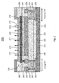
- Fig. 2 illustrates a cross-sectional view of a pixel structure 200 of an AMOLED display according to one embodiment of the invention.
- the pixel 200 of the AMOLED display includes at least structures as set forth below.
- a supporting substrate 210 has a first end portion corresponding to a driving TFT 240 and an opposite, second end portion corresponding to a read-out TFT 250.
- a semiconductor layer having a first portion 242 and a second portion 252 is correspondingly disposed on the first and second end portions of the substrate 210.
- a gate insulator layer 220 is formed on the substrate 210 and covers the semiconductor layer.
- a gate metal layer having a first portion 241 and a second portion 251 is correspondingly disposed on the two end portions of the gate insulator layer 220 via an interlayer dielectric (ILD) 230.
- ILD interlayer dielectric
- a first source metal layer 243 and a first drain metal layer 244 are electrically connected to the first portion 242 of the semiconductor layer and correspondingly disposed on the first end portion of the interlayer dielectric 230.
- a second source metal layer 253 and a second drain metal layer 254 are electrically connected to the second portion 252 of the semiconductor layer and correspondingly disposed on the second end portion of the interlayer dielectric 230.
- the first portion 241 of the gate metal layer, the first portion 242 of the semiconductor layer, the first source metal layer 243 and a first drain metal layer 244 constitute the driving TFT 240.
- the second portion 251 of the gate metal layer, the second portion 252 of the semiconductor layer, the second source metal layer 253 and a second drain metal layer 254 constitute the driving TFT 250.
- a photo sensor includes a photosensitive (Si-rich dielectric) layer 260 disposed on an extending portion 253a of the second source metal layer 253 extending to an emission region of the pixel 200 of the display.
- a first passivation layer 281 correspondingly disposed on the first and second end portions of the interlayer dielectric 230, so as to define a space therebetween in which the extending portion 253a of the second source metal layer 253 and the photosensitive layer 260 are deposed.
- a second passivation layer 282 correspondingly disposed on the first passivation layer 281.
- An OLED 270 has an anode layer 271 deposed on the photosensitive layer 260 and electrically connected to the first source metal layer 243 over the emission region of the pixel 200 of the display, an OLED emissive layer 272 disposed on and covered both the second passivation layer 282 and the anode layer 271, and a cathode layer 273 disposed on and covered the OLED emissive layer 272.
- the anode layer 271 of the OLED 270 is formed such that at least a portion that overlaps the photosensitive layer 260 of the photo sensor is partially transparent to light emitted from the emissive layer 272 of the OLED 270.
- the other portion of the anode layer 271 of the OLED 270 may or may not be transparent to light emitted from the emissive layer 272 of the OLED 270.
- the OLED 270 is a top emission OLED, i.e., the majority portion 275 of light emitted from the OLED emissive layer 272 transmits out from the cathode layer 273.
- the remaining portion 276 of the light emitted from the OLED emissive layer 272 transmits out from the anode layer 271 and to the photosensitive layer 260.
- the photo sensor measures the brightness of the remaining portion 276 of the light, i.e., an ambient light to the photo sensor, which is proportional to the light emitted from the OLED emissive layer 272, and generating a sensing signal corresponding to the measured brightness of the ambient light.
- the read-out TFT 250 reads and outputs the sensing signal.
- the sensing signal in turn, is utilized to adjust a driving voltage of the OLED 270 through the driving TFT 240 accordingly.
- Fig. 3 shows a pixel structure 300 of an AMOLED display according to another embodiment of the invention.
- the pixel structure 300 are similar to the pixel structure 200 disclosed above and shown in Fig. 2 , except that the OLED 370 is a bottom emission OLED, i.e., the light 375 emitted from the OLED emissive layer 372 transmits out from the anode layer 371.
- the anode layer 371 is formed to be transparent to light emitted from the emissive layer 372 of the OLED 370.
- the photosensitive layer 360 defines a photo sensing area that is much less than that corresponding to the top emission OLED shown in Fig. 2 .
- the photosensitive layer 360 is formed between the anode layer 371 of the OLED 370 and the second source layer 353 of the read-out TFT 350, as such the majority portion of the space defined between the diving TFT 340 and the read-out TFT 350 is corresponding to an emission region of the OLED 370.
- the majority portion of the light 375 emitted from the OLED emissive layer372 transmits out from the emission region, while the remaining portion of the light 375 transmits out from the anode layer 371 and to the photosensitive layer 360.
- the photo sensor measures the brightness of the remaining portion of the light 375, i.e., an ambient light to the photo sensor, which is proportional to the light 375 emitted from the OLED emissive layer 372, and generating a sensing signal corresponding to the measured brightness of the ambient light.
- the read-out TFT 350 reads and outputs the sensing signal.
- the sensing signal in turn, is utilized to adjust a driving voltage of the OLED 370 through the driving TFT 340 accordingly.
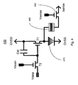
- Fig. 4 shows a circuit diagram of a pixel 400 of an AMOLED display according to yet another embodiment of the invention.
- the AMOLED display has an AMOLED panel having a plurality of pixels 400 arranged in an array.
- Each pixel 400 includes an OLED 470 having a cathode electrically coupled to a first supply voltage, OVSS, an anode and an emissive layer formed between the cathode and the anode.
- the OLED 470 can be a top-emitting OLED or a bottom-emitting OLED.
- Each pixel 400 also includes a first transistor T1 having a gate, a drain electrically coupled to a second supply voltage, OVDD, and a source electrically coupled to the anode of the OLED 470, a second transistor T2 having a gate electrically coupled to a scan signal, Vscan(N), a drain electrode electrically coupled to the gate of the first transistor T1, and a source electrode electrically coupled to a data signal, Vdata, and a storage capacitor Cst electrically connected between the gate and the drain of the first transistor T1.
- the first supply voltage OVSS and the second supply voltage OVDD are a negative supply voltage and a positive supply voltage, respectively.
- each pixel 400 includes a read-out TFT 450 having a gate electrically coupled to a sensing control voltage, Vsense, a drain for outputting a sensing signal, Isense, and a source, and a photo sensor 460 electrically coupled between the anode of the OLED 470 and the source of the read-out transistor 450.
- the photo sensor 460 is adapted for optical feedback compensation, specifically, for measuring brightness of an ambient light that is proportional to light emitted from the OLED 470 and generating the sensing signal Isense corresponding to the measured brightness of the ambient light.
- the sensing signal Isense in turn, is utilized to adjust the data signal Vdata.
- Each of the first transistor T1, the second transistor T2 and the read-out transistor 450 comprises an NMOS transistor or PMOS transistor.
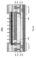
- Fig. 5 shows a pixel structure 500 of an AMOLED display according to one non-claimed embodiment.
- the display has a substrate 510, and a plurality of pixels 500 formed on the substrate 510 and arranged in an array.
- the pixel 500 includes a driving transistor 540 having a gate layer 541, a drain layer 544 and a source layer 543, formed on the substrate 510.
- the pixel 500 also includes an OLED 570 having a cathode layer 573, a anode layer 571 and an emissive layer 572 formed between the cathode layer 573 and the anode layer 571, and formed over the driving transistor 540 such that the anode layer 571 of the OLED 570 is electrically connected to the source layer 544 of the driving transistor 540.
- the pixel 500 includes a bias layer 550 formed over the substrate 510, and a photo sensor having a photosensitive layer 560 formed between the anode layer 571 of the OLED 570 and the bias layer 550.
- the driving TFT 540 is formed on one end portion of the supporting substrate 510.
- a semiconductor layer 542 is disposed on the one end portion of the substrate 510.
- a gate insulator layer 420 is disposed on the substrate 412 and covers the semiconductor layer 542.
- the gate metal layer 541 is disposed on the gate insulator layer 520 at a location that is over the semiconductor layer 542.
- An interlayer dielectric (ILD) layer 530 is deposed on the gate insulator layer 520 and covers the gate metal layer 541.
- the drain layer 544 and the source layer 543 of the driving TFT 540 are spatially formed on the interlayer dielectric layer 530 and are connected to the semiconductor layer 542.
- a metal bias electrode layer 550 is disposed on the interlayer dielectric layer 530 over the other end potion of the substrate 510 and extends into the emission region of the pixel 500.
- a photosensitive layer 560 is disposed on the metal bias electrode layer 550 at an emission region of the pixel 500.
- the anode layer 571 of the OLED 570 is disposed on the photosensitive layer 560 having one end portion electrically connected to the source layer 543 of the driving TFT 540, and the other end portion extended over the other end portion of the substrate 510.
- a first passivation layer 581 is correspondingly disposed on the two ends of the interlayer dielectric 530 so that the emission region of the pixel 500 is defined therebetween.
- a second passivation layer 582 is correspondingly disposed on the first passivation layer 581.
- the OLED emissive layer 572 of the OLED 570 is disposed on the anode layer 571 and covers both the second passivation layer 582 and the anode layer 571.
- the cathode layer 573 of the OLED 570 is disposed on and covers the OLED emissive layer 572 of the OLED 570.
- the OLED 570 is a top emission OLED, i.e., the majority portion 575 of light emitted from the OLED emissive layer 572 transmits out from the cathode layer 573.
- the remaining portion 576 of the light emitted from the OLED emissive layer 572 transmits out from the anode layer 573 and to the photosensitive layer 560.
- the photo sensor measures the brightness of the remaining portion 576 of the light, an ambient light to the photo sensor, which is proportional to the light emitted from the OLED emissive layer 572, and generating a sensing signal corresponding to the measured brightness of the ambient light.
- the read-out TFT 550 reads and outputs the sensing signal.
- the sensing signal is output from the bias electrode 560 and utilized to adjust a driving voltage of the OLED 570 through the driving TFT 540 accordingly.
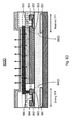
- Fig. 6 shows a pixel structure 600 of an AMOLED display according to another non-claimed embodiment.
- the pixel structure 600 are similar to the pixel structure 500 disclosed above and shown in Fig. 5 , except that the OLED 670 is a bottom emission OLED, i.e., the light 675 emitted from the OLED emissive layer 672 transmits out from the anode layer 671.
- the photosensitive layer 660 defines a photo sensing area that is much less than that corresponding to the top emission OLED shown in Fig. 5 .
- the photosensitive layer 660 is formed between the anode layer 671 of the OLED 670 and the bias electrode 650, as such the majority portion of the space defined between the diving TFT 640 and the bias electrode 650 is corresponding to an emission region of the OLED 670.
- the majority portion of the light 675 emitted from the OLED emissive layer 672 transmits out from the emission region, while the remaining portion of the light 675 transmits out from the anode layer 671 and to the photosensitive layer 660.
- the photo sensor measures the brightness of the remaining portion of the light 675, i.e., an ambient light to the photo sensor, which is proportional to the light 675 emitted from the OLED emissive layer 672, and generating a sensing signal corresponding to the measured brightness of the ambient light.
- the bias electrode 650 outputs the sensing signal.
- the sensing signal in turn, is utilized to adjust a driving voltage of the OLED 670 through the driving TFT 640 accordingly.
- Fig. 7 shows a circuit diagram of a pixel 700 of an AMOLED display according to yet another non-claimed embodiment.
- the AMOLED display has an AMOLED panel having a plurality of pixels 700 arranged in an array.
- Each pixel 700 includes an OLED 770 having a cathode electrically coupled to a first supply voltage, OVSS, an anode and an emissive layer formed between the cathode and the anode.
- the OLED 770 can be a top-emitting OLED or a bottom-emitting OLED.
- Each pixel 700 also includes a first transistor T1 having a gate, a drain electrically coupled to a second supply voltage, OVDD, and a source electrically coupled to the anode of the OLED 770, a second transistor T2 having a gate electrically coupled to a scan signal, Vscan(N), a drain electrode electrically coupled to the gate of the first transistor T1, and a source electrode electrically coupled to a data signal, Vdata, and a storage capacitor Cst electrically connected between the gate and the drain of the first transistor T1.
- the first supply voltage OVSS and the second supply voltage OVDD are a negative supply voltage and a positive supply voltage, respectively.
- Each of the first transistor T1 and the second transistor T2 comprises an NMOS transistor or PMOS transistor.
- each pixel 700 includes a photo sensor 760 electrically coupled to the anode of the OLED 770 for measuring brightness of an ambient light that is proportional to light emitted from the OLED 770 and generating the sensing signal I 2 corresponding to the measured brightness of the ambient light, and a bias electrode (line) 750 electrically coupled to the photo sensor 760 for outputting the sensing signal I 2 .
- the generated current of the OLED 770, I OLED (I 1 - I 2 ), where I 1 is the current flow from the drain to the source of the first TFT T1, and I 2 is the sensing current of the photo sensor 760 that is output from the bias line 750.
- the sensing current I 2 is adapted for optical feedback compensation.
- the photo sensor current I2 increases, which in turn, results in a decrease of the OLED current I OLED , so that the light of the OLED 770 become darker.
- the photo sensor current I2 decreases, which in turn, results in an increase of the OLED current I OLED , so that the light of the OLED 770 become brighter.
- the AMOLED display panel will not generate line mura during operation, largely improving the display quality of the AMOLED display panel.
- Figs. 8A-8D disclose a pixel structure of an AMOLED display according to four different embodiments 800A-800D of the invention. Each embodiment corresponds to a different type of the driving TFT and the read-out TFT. In these embodiments, each of the driving TFT and the read-out TFT is formed with a semiconductive layer 842/852, a gate layer841/851, a source layer 843/853 and a drain layer 844/854. Different fabrication processes produce different type TFTs.
- the driving TFT 840A and the read-out TFT 850A are respectively formed in a bottom gate type TFT.
- Fig. 8B shows the driving TFT 840B and the read-out TFT 850B respectively formed in a coplanar type TFT.
- Fig. 8C shows the driving TFT 840C and the read-out TFT 850C respectively formed in a back channel etched (BCE) type TFT.
- Fig. 8D shows the driving TFT 840D and the read-out TFT 850D respectively formed in an IS type TFT, where an etch stop layer 845/855 is deposed on the semiconductive layer 842/852.
- the supporting substrate which can include, but not limited to, glass, plastic, semiconductor materials, silicon, ceramics, and circuit board materials.
- the semiconductor layer can include, but not limited to, polysilicon, (coplanar/IS/BCE structure) metal oxide materials such as IZO, IGZO, AnO and In 2 O 3 .
- the gate insulator layer can include, but not limited to, SiOx, SiNx, SiOx/SiNx and AlOx.
- the gate metal layer can include, but not limited to, Mo, AlNd, Ti/AlTi, Mo/Al/Mo and Cu.
- the interlayer dielectric layer can include, but not limited to, SiOx, SiNx and SiOx/SiNx.
- the etch stop layer can include, but not limited to, SiOx, SiNx and AlOx.
- the source/drain metal layer can include, but not limited to, Mo, AINd, Ti/Al/Ti, Mo/AI/Mo and Cu.
- the metal bias line layer can include, but not limited to, Mo, AiNd, Ti/Al/Ti, Mo/AI/Mo and Cu.
- the photsenstive layer can include, but not limited to, Si-rch dielectric or other photosensitive materials.
- the anode layer can include, but not limited to, ITO, IZO, AI, Ag, AI/ITO, Ag/ITO, ITO/Ag/ITO and Mo/Al/ITO.
- the first passivation layer can include, but not limited to, SiOx, SiNx, SiOx/organic materials, SiNx/organic materials and organic materials.
- the second passivation layer can include, but not limited to, SiOX, SiNx and organice materials.
- One aspect of the present invention relates to a method of driving a display in accordance with claim 1 and having an active matrix organic light emitting diode (AMOLED) panel having a plurality of pixels arranged in an array, each pixel comprising an organic light emitting diode (OLED).
- the method includes the steps of measuring brightness of an ambient light that is proportional to light emitted from the OLED so as to generate a sensing signal corresponding to the measured brightness of the ambient light, and adjusting a driving voltage of the OLED according to the sensing signal.
- the measuring step is performed with a photo sensor coupled to the OLED.
- the present invention discloses an AMOLED display with each pixel incorporated with a photo sensor for optical feedback compensation so as to improve the performance of the AMOLED display.
Description
- The present invention relates generally to an organic light emitting diode (OLED) display, and more particularly, to an active matrix organic light emitting diode (AMOLED) display having each pixel structure incorporated with a photo sensor for optical feedback compensation so as to improve the performance of the AMOLED display.
- Organic light emitting diode (OLED) panel has a faster response, lighter weight, lesser viewing angle restrictions and greater contrast compared with a liquid crystal display panel, and thus has drawn great attention of the display industry. The OLED panel can be classified as a passive matrix organic light emitting diode (PMOLED) panel or an active matrix organic light emitting diode (AMOLED) panel. Generally, the AMOLED panel is particularly adapted to the production of high resolution and large size display panels.
- The brightness of a pixel in the AMOLED panel is proportional to the conducting current of the organic light emitting diode and the conducting current is decided by thin film transistors (TFTs). In other words, the emission property, such as brightness and uniformity of emitted light, of the AMOLED is very sensitive to the performance of the TFTs.
- Particularly, for an AMOLED display panel having a low-temperature polysilicon (LTPS) backplane crystallized by the excimer laser anneling (ELA), crystallization and non-uniformity of defeats may result in a line mura effect in the display panel, as shown in
Fig. 1 . The mura defects are defects that exhibit as non-uniform contract regions on OLED display pane and are attributed to pulse-to-pulse variations in the laser beam energy that is used to crystallize the amorphous silicon film. These defects are more pronounced when a constant gray value image or pattern is displayed. In AMOLED display panels, the laser annal irradiation of the non-TFT regions, such as the OLED circuit portion, on the TFT back panel often results in line-shaped mura defects. The non-uniform laser beam energy caused by pulse-to-pulse variations in the laser beam energy results in a non-uniform performance of polycrystalline silicon. Since the TFT characteristic is sensitive to the performance of the polycrystalline silicon, and the TFT devices drive the OLED devices, the non-uniform TFT characteristics result in non-uniformity in OLED's brightness. This non-uniformity causes the line mura defects, which deteriorate the display quality of the AMOLED display panel. - Therefore, a heretofore unaddressed need exists in the art to address the aforementioned deficiencies and inadequacies.
-
US 2001/028060 A1 relates to a semiconductor display device including a plurality of pixels. Each pixel includes an electroluminescence element a plurality of transistors and a photo sensing diode. However, document D1 does not refer to a control mechanism for the intensity of the diode. Further examples for display devices are described by Xue J. et al. ("Organic optical bistable switch", Applied Physics Letters, AIP, Melville, US, vol.82, No.1, January 6, 2003, pages 136 to 138, XP012033419),US 2004/031966 A1 ,US 2006/097296 A1 andUS 2007/257250 A1 . - Starting from the prior art, it is the object of the present application to provide a display which has improved performance properties.
- The above-mentioned object is solved by the display according to
claim 1, which incorporates a photo sensor for optical feedback compensation. Advantageous improvements of the invention are described by dependant claims. - The anode layer of the OLED may be formed such that at least a portion that overlaps the photosensitive layer of the photo sensor is partially transparent to light emitted from the emissive layer of the OLED. The photo sensor is adapted for measuring brightness of an ambient light that is proportional to light emitted from the OLED and generates a sensing signal corresponding to the measured brightness of the ambient light, wherein the sensing signal is utilized to adjust a driving voltage of the OLED accordingly.
- The OLED may include a top-emitting OLED or a bottom-emitting OLED. In one embodiment, the photosensitive layer defines a photo sensing area, where the photo sensing area for the top-emitting OLED is larger than that for bottom-emitting OLED. In one embodiment, the photosensitive layer is formed of a Si-rich dielectric material.
- In one embodiment, each of the driving transistor and the read-out transistor comprises an NMOS transistor or PMOS transistor. Each of the driving transistor and the read-out transistor comprises a back channel etched (BCE) type thin film transistor (TFT), an IS type TFT, a coplanar type TFT, a bottom-gate type TFT, or a top-gate type TFT.
- The first supply voltage OVSS and the second supply voltage OVDD may be a negative supply voltage and a positive supply voltage, respectively.
- In one aspect, the present invention relates to a method of driving a display as recited in
claim 1, the display having an active matrix organic light emitting diode (AMOLED) panel having a plurality of pixels arranged in an array, each pixel comprising an organic light emitting diode (OLED). In one embodiment, the method includes the steps of measuring brightness of an ambient light that is proportional to light emitted from the OLED so as to generate a sensing signal corresponding to the measured brightness of the ambient light, and adjusting a driving voltage of the OLED according to the sensing signal. - In one embodiment, the measuring step is performed with a photo sensor coupled to the OLED.
- The accompanying drawings illustrate one or more embodiments of the invention and, together with the written description, serve to explain the principles of the invention. Wherever possible, the same reference numbers are used throughout the drawings to refer to the same or like elements of an embodiment, and wherein:
-
Fig. 1 shows a conventional AMOLED display panel with the line mura defect problem; -
Fig. 2 shows a schematic cross-sectional view illustrating a top emission AMOLED pixel structure according to one embodiment of the invention; -
Fig. 3 shows a schematic cross-sectional view illustrating a bottom emission AMOLED pixel structure according to another embodiment of the invention; -
Fig. 4 shows a schematic circuit diagram of a pixel structure of the AMOLED display according to one embodiment of the invention; -
Fig. 5 shows a schematic cross-sectional view illustrating a top emission AMOLED pixel structure according to one non-claimed embodiment; -
Fig. 6 shows a schematic cross-sectional view illustrating a bottom emission AMOLED pixel structure according to another non-claimed embodiment; -
Fig. 7 shows a schematic circuit diagram of a pixel structure of the AMOLED display according to one non-claimed embodiment; and -
Figs. 8A-8D show schematically cross-sectional views illustrating a top emission AMOLED pixel structure according to various embodiments of the invention. - The present disclosure is more particularly described in the following examples that are intended as illustrative only since numerous modifications and variations therein will be apparent to those skilled in the art. Various embodiments of the disclosure are now described in detail. Referring to the drawings, like numbers indicate like components throughout the views. As used in the description herein and throughout the claims that follow, the meaning of "a", "an", and "the" includes plural reference unless the context clearly dictates otherwise. Also, as used in the description herein and throughout the claims that follow, the meaning of "in" includes "in" and "on" unless the context clearly dictates otherwise.
- The terms used in this specification generally have their ordinary meanings in the art, within the context of the disclosure, and in the specific context where each term is used. Certain terms that are used to describe the disclosure are discussed below, or elsewhere in the specification, to provide additional guidance to the practitioner regarding the description of the disclosure. The use of examples anywhere in this specification, including examples of any terms discussed herein, is illustrative only, and in no way limits the scope and meaning of the disclosure or of any exemplified term. Likewise, the disclosure is not limited to various embodiments given in this specification.
- As used herein, the terms "comprising," "including," "having," "containing," "involving," and the like are to be understood to be open-ended, i.e., to mean including but not limited to.
- The present invention can be employed in most OLED display configurations. These include very simple structures comprising single anode and cathode to more complex displays, such as passive matrix displays including orthogoanl arrays of anodes and cathodes to form light emitting elements, and active matrix displays where each light emitting element is controlled independently, for example, within thin film transistors. In accordance with the purposes of this invention, as embodied and broadly described herein, this invention, in one aspect, relates to an improved layout of AMOLED pixel structure which incorporates a photo sensitive layer to serve as a photo sensor for optical feedback compensation.
-
Fig. 2 illustrates a cross-sectional view of apixel structure 200 of an AMOLED display according to one embodiment of the invention. In this exemplary embodiment, thepixel 200 of the AMOLED display includes at least structures as set forth below. A supportingsubstrate 210 has a first end portion corresponding to a drivingTFT 240 and an opposite, second end portion corresponding to a read-out TFT 250. A semiconductor layer having afirst portion 242 and asecond portion 252 is correspondingly disposed on the first and second end portions of thesubstrate 210. Agate insulator layer 220 is formed on thesubstrate 210 and covers the semiconductor layer. A gate metal layer having afirst portion 241 and asecond portion 251 is correspondingly disposed on the two end portions of thegate insulator layer 220 via an interlayer dielectric (ILD) 230. A firstsource metal layer 243 and a firstdrain metal layer 244 are electrically connected to thefirst portion 242 of the semiconductor layer and correspondingly disposed on the first end portion of theinterlayer dielectric 230. A secondsource metal layer 253 and a seconddrain metal layer 254 are electrically connected to thesecond portion 252 of the semiconductor layer and correspondingly disposed on the second end portion of theinterlayer dielectric 230. Thefirst portion 241 of the gate metal layer, thefirst portion 242 of the semiconductor layer, the firstsource metal layer 243 and a firstdrain metal layer 244 constitute the drivingTFT 240. Thesecond portion 251 of the gate metal layer, thesecond portion 252 of the semiconductor layer, the secondsource metal layer 253 and a seconddrain metal layer 254 constitute the drivingTFT 250. - A photo sensor includes a photosensitive (Si-rich dielectric)
layer 260 disposed on an extendingportion 253a of the secondsource metal layer 253 extending to an emission region of thepixel 200 of the display. Afirst passivation layer 281 correspondingly disposed on the first and second end portions of theinterlayer dielectric 230, so as to define a space therebetween in which the extendingportion 253a of the secondsource metal layer 253 and thephotosensitive layer 260 are deposed. Asecond passivation layer 282 correspondingly disposed on thefirst passivation layer 281. - An
OLED 270 has ananode layer 271 deposed on thephotosensitive layer 260 and electrically connected to the firstsource metal layer 243 over the emission region of thepixel 200 of the display, an OLEDemissive layer 272 disposed on and covered both thesecond passivation layer 282 and theanode layer 271, and acathode layer 273 disposed on and covered the OLEDemissive layer 272. Theanode layer 271 of theOLED 270 is formed such that at least a portion that overlaps thephotosensitive layer 260 of the photo sensor is partially transparent to light emitted from theemissive layer 272 of theOLED 270. The other portion of theanode layer 271 of theOLED 270 may or may not be transparent to light emitted from theemissive layer 272 of theOLED 270. - In this embodiment, the
OLED 270 is a top emission OLED, i.e., themajority portion 275 of light emitted from the OLEDemissive layer 272 transmits out from thecathode layer 273. The remainingportion 276 of the light emitted from the OLEDemissive layer 272 transmits out from theanode layer 271 and to thephotosensitive layer 260. Accordingly, the photo sensor measures the brightness of the remainingportion 276 of the light, i.e., an ambient light to the photo sensor, which is proportional to the light emitted from the OLEDemissive layer 272, and generating a sensing signal corresponding to the measured brightness of the ambient light. The read-outTFT 250 reads and outputs the sensing signal. The sensing signal in turn, is utilized to adjust a driving voltage of theOLED 270 through the drivingTFT 240 accordingly. -
Fig. 3 shows apixel structure 300 of an AMOLED display according to another embodiment of the invention. Thepixel structure 300 are similar to thepixel structure 200 disclosed above and shown inFig. 2 , except that theOLED 370 is a bottom emission OLED, i.e., the light 375 emitted from the OLEDemissive layer 372 transmits out from theanode layer 371. Theanode layer 371 is formed to be transparent to light emitted from theemissive layer 372 of theOLED 370. Accordingly, thephotosensitive layer 360 defines a photo sensing area that is much less than that corresponding to the top emission OLED shown inFig. 2 . Thephotosensitive layer 360 is formed between theanode layer 371 of theOLED 370 and thesecond source layer 353 of the read-outTFT 350, as such the majority portion of the space defined between thediving TFT 340 and the read-outTFT 350 is corresponding to an emission region of theOLED 370. In operation, the majority portion of the light 375 emitted from the OLED emissive layer372 transmits out from the emission region, while the remaining portion of the light 375 transmits out from theanode layer 371 and to thephotosensitive layer 360. Accordingly, the photo sensor measures the brightness of the remaining portion of the light 375, i.e., an ambient light to the photo sensor, which is proportional to the light 375 emitted from the OLEDemissive layer 372, and generating a sensing signal corresponding to the measured brightness of the ambient light. The read-outTFT 350 reads and outputs the sensing signal. The sensing signal in turn, is utilized to adjust a driving voltage of theOLED 370 through the drivingTFT 340 accordingly. -
Fig. 4 shows a circuit diagram of apixel 400 of an AMOLED display according to yet another embodiment of the invention. The AMOLED display has an AMOLED panel having a plurality ofpixels 400 arranged in an array. Eachpixel 400 includes anOLED 470 having a cathode electrically coupled to a first supply voltage, OVSS, an anode and an emissive layer formed between the cathode and the anode. TheOLED 470 can be a top-emitting OLED or a bottom-emitting OLED. Eachpixel 400 also includes a first transistor T1 having a gate, a drain electrically coupled to a second supply voltage, OVDD, and a source electrically coupled to the anode of theOLED 470, a second transistor T2 having a gate electrically coupled to a scan signal, Vscan(N), a drain electrode electrically coupled to the gate of the first transistor T1, and a source electrode electrically coupled to a data signal, Vdata, and a storage capacitor Cst electrically connected between the gate and the drain of the first transistor T1. The first supply voltage OVSS and the second supply voltage OVDD are a negative supply voltage and a positive supply voltage, respectively. - Further, each
pixel 400 includes a read-outTFT 450 having a gate electrically coupled to a sensing control voltage, Vsense, a drain for outputting a sensing signal, Isense, and a source, and aphoto sensor 460 electrically coupled between the anode of theOLED 470 and the source of the read-outtransistor 450. Thephoto sensor 460 is adapted for optical feedback compensation, specifically, for measuring brightness of an ambient light that is proportional to light emitted from theOLED 470 and generating the sensing signal Isense corresponding to the measured brightness of the ambient light. The sensing signal Isense in turn, is utilized to adjust the data signal Vdata. - Each of the first transistor T1, the second transistor T2 and the read-out
transistor 450 comprises an NMOS transistor or PMOS transistor. -
Fig. 5 shows apixel structure 500 of an AMOLED display according to one non-claimed embodiment. The display has asubstrate 510, and a plurality ofpixels 500 formed on thesubstrate 510 and arranged in an array. Thepixel 500 includes a drivingtransistor 540 having agate layer 541, adrain layer 544 and asource layer 543, formed on thesubstrate 510. Thepixel 500 also includes anOLED 570 having acathode layer 573, aanode layer 571 and anemissive layer 572 formed between thecathode layer 573 and theanode layer 571, and formed over the drivingtransistor 540 such that theanode layer 571 of theOLED 570 is electrically connected to thesource layer 544 of the drivingtransistor 540. Further, thepixel 500 includes abias layer 550 formed over thesubstrate 510, and a photo sensor having aphotosensitive layer 560 formed between theanode layer 571 of theOLED 570 and thebias layer 550. - More specifically, the driving
TFT 540 is formed on one end portion of the supportingsubstrate 510. Asemiconductor layer 542 is disposed on the one end portion of thesubstrate 510. A gate insulator layer 420 is disposed on the substrate 412 and covers thesemiconductor layer 542. Thegate metal layer 541 is disposed on thegate insulator layer 520 at a location that is over thesemiconductor layer 542. An interlayer dielectric (ILD)layer 530 is deposed on thegate insulator layer 520 and covers thegate metal layer 541. Thedrain layer 544 and thesource layer 543 of the drivingTFT 540 are spatially formed on theinterlayer dielectric layer 530 and are connected to thesemiconductor layer 542. Further, a metalbias electrode layer 550 is disposed on theinterlayer dielectric layer 530 over the other end potion of thesubstrate 510 and extends into the emission region of thepixel 500. - A
photosensitive layer 560 is disposed on the metalbias electrode layer 550 at an emission region of thepixel 500. Theanode layer 571 of theOLED 570 is disposed on thephotosensitive layer 560 having one end portion electrically connected to thesource layer 543 of the drivingTFT 540, and the other end portion extended over the other end portion of thesubstrate 510. Afirst passivation layer 581 is correspondingly disposed on the two ends of theinterlayer dielectric 530 so that the emission region of thepixel 500 is defined therebetween. Asecond passivation layer 582 is correspondingly disposed on thefirst passivation layer 581. The OLEDemissive layer 572 of theOLED 570 is disposed on theanode layer 571 and covers both thesecond passivation layer 582 and theanode layer 571. Thecathode layer 573 of theOLED 570 is disposed on and covers the OLEDemissive layer 572 of theOLED 570. - In the exemplary embodiment shown in
Fig. 5 , theOLED 570 is a top emission OLED, i.e., themajority portion 575 of light emitted from the OLEDemissive layer 572 transmits out from thecathode layer 573. The remainingportion 576 of the light emitted from the OLEDemissive layer 572 transmits out from theanode layer 573 and to thephotosensitive layer 560. Accordingly, the photo sensor measures the brightness of the remainingportion 576 of the light, an ambient light to the photo sensor, which is proportional to the light emitted from the OLEDemissive layer 572, and generating a sensing signal corresponding to the measured brightness of the ambient light. The read-outTFT 550 reads and outputs the sensing signal. The sensing signal is output from thebias electrode 560 and utilized to adjust a driving voltage of theOLED 570 through the drivingTFT 540 accordingly. -
Fig. 6 shows apixel structure 600 of an AMOLED display according to another non-claimed embodiment. Thepixel structure 600 are similar to thepixel structure 500 disclosed above and shown inFig. 5 , except that theOLED 670 is a bottom emission OLED, i.e., the light 675 emitted from the OLEDemissive layer 672 transmits out from theanode layer 671. Accordingly, thephotosensitive layer 660 defines a photo sensing area that is much less than that corresponding to the top emission OLED shown inFig. 5 . Thephotosensitive layer 660 is formed between theanode layer 671 of theOLED 670 and thebias electrode 650, as such the majority portion of the space defined between thediving TFT 640 and thebias electrode 650 is corresponding to an emission region of theOLED 670. In operation, the majority portion of the light 675 emitted from the OLEDemissive layer 672 transmits out from the emission region, while the remaining portion of the light 675 transmits out from theanode layer 671 and to thephotosensitive layer 660. Accordingly, the photo sensor measures the brightness of the remaining portion of the light 675, i.e., an ambient light to the photo sensor, which is proportional to the light 675 emitted from the OLEDemissive layer 672, and generating a sensing signal corresponding to the measured brightness of the ambient light. Thebias electrode 650 outputs the sensing signal. The sensing signal in turn, is utilized to adjust a driving voltage of theOLED 670 through the drivingTFT 640 accordingly. -
Fig. 7 shows a circuit diagram of apixel 700 of an AMOLED display according to yet another non-claimed embodiment. The AMOLED display has an AMOLED panel having a plurality ofpixels 700 arranged in an array. Eachpixel 700 includes anOLED 770 having a cathode electrically coupled to a first supply voltage, OVSS, an anode and an emissive layer formed between the cathode and the anode. TheOLED 770 can be a top-emitting OLED or a bottom-emitting OLED. Eachpixel 700 also includes a first transistor T1 having a gate, a drain electrically coupled to a second supply voltage, OVDD, and a source electrically coupled to the anode of theOLED 770, a second transistor T2 having a gate electrically coupled to a scan signal, Vscan(N), a drain electrode electrically coupled to the gate of the first transistor T1, and a source electrode electrically coupled to a data signal, Vdata, and a storage capacitor Cst electrically connected between the gate and the drain of the first transistor T1. The first supply voltage OVSS and the second supply voltage OVDD are a negative supply voltage and a positive supply voltage, respectively. Each of the first transistor T1 and the second transistor T2 comprises an NMOS transistor or PMOS transistor. - Further, each
pixel 700 includes aphoto sensor 760 electrically coupled to the anode of theOLED 770 for measuring brightness of an ambient light that is proportional to light emitted from theOLED 770 and generating the sensing signal I2 corresponding to the measured brightness of the ambient light, and a bias electrode (line) 750 electrically coupled to thephoto sensor 760 for outputting the sensing signal I2. The generated current of theOLED 770, IOLED = (I1 - I2), where I1 is the current flow from the drain to the source of the first TFT T1, and I2 is the sensing current of thephoto sensor 760 that is output from thebias line 750. According to the invention, the sensing current I2 is adapted for optical feedback compensation. For example, for a pixel driven under the same value of Vdata, if a small value of Vth_T1 results in a large I1, the light emitted from theOLED 770 will be brighter. Accordingly, the photo sensor current I2 increases, which in turn, results in a decrease of the OLED current IOLED, so that the light of theOLED 770 become darker. On the other hand, if a large value of Vth_T1 results in a small I1, the light emitted from theOLED 770 will be darker. Accordingly, the photo sensor current I2 decreases, which in turn, results in an increase of the OLED current IOLED, so that the light of theOLED 770 become brighter. As a result, the AMOLED display panel will not generate line mura during operation, largely improving the display quality of the AMOLED display panel. - The above disclosed driving TFT and the read-out TFT, as shown in
Figs. 2 ,3 ,5 and6 , are corresponding to top-gate type TFTs. Other types of TFFs can also be used as the driving TFT and the read-out TFT to practice the invention.Figs. 8A-8D disclose a pixel structure of an AMOLED display according to fourdifferent embodiments 800A-800D of the invention. Each embodiment corresponds to a different type of the driving TFT and the read-out TFT. In these embodiments, each of the driving TFT and the read-out TFT is formed with asemiconductive layer 842/852, a gate layer841/851, asource layer 843/853 and adrain layer 844/854. Different fabrication processes produce different type TFTs. - For example, as shown in
Fig. 8A , the drivingTFT 840A and the read-outTFT 850A are respectively formed in a bottom gate type TFT.Fig. 8B shows the driving TFT 840B and the read-out TFT 850B respectively formed in a coplanar type TFT.Fig. 8C shows the drivingTFT 840C and the read-outTFT 850C respectively formed in a back channel etched (BCE) type TFT. AndFig. 8D shows the drivingTFT 840D and the read-outTFT 850D respectively formed in an IS type TFT, where anetch stop layer 845/855 is deposed on thesemiconductive layer 842/852. - As to the materials forming the pixel structure, the supporting substrate, which can include, but not limited to, glass, plastic, semiconductor materials, silicon, ceramics, and circuit board materials. The semiconductor layer can include, but not limited to, polysilicon, (coplanar/IS/BCE structure) metal oxide materials such as IZO, IGZO, AnO and In2O3. The gate insulator layer can include, but not limited to, SiOx, SiNx, SiOx/SiNx and AlOx. The gate metal layer can include, but not limited to, Mo, AlNd, Ti/AlTi, Mo/Al/Mo and Cu. The interlayer dielectric layer can include, but not limited to, SiOx, SiNx and SiOx/SiNx. The etch stop layer, as shown in
Fig. 8D , can include, but not limited to, SiOx, SiNx and AlOx. The source/drain metal layer can include, but not limited to, Mo, AINd, Ti/Al/Ti, Mo/AI/Mo and Cu. The metal bias line layer can include, but not limited to, Mo, AiNd, Ti/Al/Ti, Mo/AI/Mo and Cu. The photsenstive layer can include, but not limited to, Si-rch dielectric or other photosensitive materials. The anode layer can include, but not limited to, ITO, IZO, AI, Ag, AI/ITO, Ag/ITO, ITO/Ag/ITO and Mo/Al/ITO. The first passivation layer can include, but not limited to, SiOx, SiNx, SiOx/organic materials, SiNx/organic materials and organic materials. The second passivation layer can include, but not limited to, SiOX, SiNx and organice materials. - One aspect of the present invention relates to a method of driving a display in accordance with
claim 1 and having an active matrix organic light emitting diode (AMOLED) panel having a plurality of pixels arranged in an array, each pixel comprising an organic light emitting diode (OLED). In one embodiment, the method includes the steps of measuring brightness of an ambient light that is proportional to light emitted from the OLED so as to generate a sensing signal corresponding to the measured brightness of the ambient light, and adjusting a driving voltage of the OLED according to the sensing signal. - The measuring step is performed with a photo sensor coupled to the OLED.
- In sum, the present invention discloses an AMOLED display with each pixel incorporated with a photo sensor for optical feedback compensation so as to improve the performance of the AMOLED display.
Claims (4)
- A display, comprising:an active matrix organic light emitting diode (AMOLED) panel having a plurality of pixels (400) arranged in an array, each pixel (400) comprising:(a) an organic light emitting diode (470) having a cathode electrically coupled to a first supply voltage (OVSS), a anode and an emissive layer formed between the cathode and the anode;(b) a driving circuit having:(i) a first transistor (T1) having a gate, a drain electrically coupled to a second supply voltage( OVDD) and a source electrically coupled to the anode of the organic light emitting diode (470);(ii) a second transistor (T2) having a gate electrically coupled to a scan signal (Vscan(N)), a drain electrode electrically coupled to the gate of the first transistor (T1), and a source electrode electrically coupled to a data signal (Vdata); and(iii) a storage capacitor (Cst) electrically connected between the gate and the drain of the first transistor (T1);(c) a read-out transistor (450) having a gate electrically a sensing control voltage (Vsense), a drain for outputting a sensing signal (Isense), and a source; and(d) a photo sensor (460)characterized in thatthe photo sensor (460) is electrically coupled between the anode of the organic light emitting diode (450) and the source of the read-out transistor (450),wherein the photo sensor (460) is adapted for measuring brightness of an ambient light that is proportional to light emitted from the organic light emitting diode (450) and for generating a sensing signal (Vbias) corresponding to the measured brightness of the ambient light, wherein the data signal (Vdata) is adjusted according to the sensing signal (Vbias).
- The display of claim 1, wherein the organic light emitting diode (470) comprises a top-emitting OLED or a bottom-emitting OLED.
- The display of claim 2, wherein the photosensitive layer defines a photo sensing area, wherein the photo sensing area for the top-emitting OLED is larger than that for bottom-emitting OLED.
- The display of claim 1, wherein each of the transistors (T1, T2, 460) comprises an NMOS transistor or PMOS transistor.
Priority Applications (2)
| Application Number | Priority Date | Filing Date | Title |
|---|---|---|---|
| EP15180452.3A EP2998996B1 (en) | 2010-03-11 | 2010-08-16 | Amoled display with optical feedback compensation |
| EP18193904.2A EP3499575A1 (en) | 2010-03-11 | 2010-08-16 | Amoled display with optical feedback compensation |
Applications Claiming Priority (1)
| Application Number | Priority Date | Filing Date | Title |
|---|---|---|---|
| US12/722,040 US8669924B2 (en) | 2010-03-11 | 2010-03-11 | Amoled display with optical feedback compensation |
Related Child Applications (3)
| Application Number | Title | Priority Date | Filing Date |
|---|---|---|---|
| EP18193904.2A Division EP3499575A1 (en) | 2010-03-11 | 2010-08-16 | Amoled display with optical feedback compensation |
| EP15180452.3A Division EP2998996B1 (en) | 2010-03-11 | 2010-08-16 | Amoled display with optical feedback compensation |
| EP15180452.3A Division-Into EP2998996B1 (en) | 2010-03-11 | 2010-08-16 | Amoled display with optical feedback compensation |
Publications (3)
| Publication Number | Publication Date |
|---|---|
| EP2365529A2 EP2365529A2 (en) | 2011-09-14 |
| EP2365529A3 EP2365529A3 (en) | 2012-08-01 |
| EP2365529B1 true EP2365529B1 (en) | 2015-09-16 |
Family
ID=43431979
Family Applications (3)
| Application Number | Title | Priority Date | Filing Date |
|---|---|---|---|
| EP15180452.3A Active EP2998996B1 (en) | 2010-03-11 | 2010-08-16 | Amoled display with optical feedback compensation |
| EP10172977.0A Active EP2365529B1 (en) | 2010-03-11 | 2010-08-16 | AMOLED display with optical feedback compensation |
| EP18193904.2A Withdrawn EP3499575A1 (en) | 2010-03-11 | 2010-08-16 | Amoled display with optical feedback compensation |
Family Applications Before (1)
| Application Number | Title | Priority Date | Filing Date |
|---|---|---|---|
| EP15180452.3A Active EP2998996B1 (en) | 2010-03-11 | 2010-08-16 | Amoled display with optical feedback compensation |
Family Applications After (1)
| Application Number | Title | Priority Date | Filing Date |
|---|---|---|---|
| EP18193904.2A Withdrawn EP3499575A1 (en) | 2010-03-11 | 2010-08-16 | Amoled display with optical feedback compensation |
Country Status (4)
| Country | Link |
|---|---|
| US (2) | US8669924B2 (en) |
| EP (3) | EP2998996B1 (en) |
| CN (1) | CN101976679B (en) |
| TW (1) | TWI496279B (en) |
Families Citing this family (62)
| Publication number | Priority date | Publication date | Assignee | Title |
|---|---|---|---|---|
| US9183779B2 (en) | 2012-02-23 | 2015-11-10 | Broadcom Corporation | AMOLED light sensing |
| TWI480998B (en) * | 2012-05-24 | 2015-04-11 | Au Optronics Corp | Structure, manufacturing method and driving circuit of organic light emitting pixel |
| CN102664187B (en) * | 2012-05-29 | 2016-01-20 | 南京中电熊猫液晶显示科技有限公司 | Organic light emitting diode display and manufacture method thereof |
| CN102760755B (en) * | 2012-07-27 | 2015-07-15 | 南京中电熊猫液晶显示科技有限公司 | Metal oxide organic light-emitting diode (OLED) display device and manufacturing method thereof |
| US9666119B2 (en) | 2012-08-30 | 2017-05-30 | Apple Inc. | Systems and methods for controlling current in display devices |
| US9019253B2 (en) | 2012-08-30 | 2015-04-28 | Apple Inc. | Methods and systems for adjusting color gamut in response to ambient conditions |
| KR20140064328A (en) * | 2012-11-20 | 2014-05-28 | 엘지디스플레이 주식회사 | Organic electro-luminescent device and method of fabricating the same |
| US8952947B2 (en) * | 2012-12-07 | 2015-02-10 | Htc Corporation | Display method for sunlight readable and electronic device using the same |
| US9111757B2 (en) | 2013-04-25 | 2015-08-18 | Apple Inc. | Display having a backplane with interlaced laser crystallized regions |
| TWI486839B (en) * | 2013-06-03 | 2015-06-01 | Ye Xin Technology Consulting Co Ltd | Touch display device |
| TWI516028B (en) * | 2013-06-20 | 2016-01-01 | 財團法人工業技術研究院 | Embedded power module for high/low voltage insulation |
| EP2860720A1 (en) * | 2013-10-10 | 2015-04-15 | Nederlandse Organisatie voor toegepast- natuurwetenschappelijk onderzoek TNO | Electro-optical unit for a picture element that can be programmed by electromagnetic radiation |
| KR102116896B1 (en) | 2013-10-14 | 2020-06-01 | 삼성디스플레이 주식회사 | Organic light emitting diode display |
| KR20150043136A (en) | 2013-10-14 | 2015-04-22 | 삼성디스플레이 주식회사 | Organic light emitting display device and manufacturing method thereof |
| KR102207563B1 (en) | 2013-10-29 | 2021-01-27 | 삼성디스플레이 주식회사 | Organic light emitting display devices and methods of manufacturing organic light emitting display devices |
| KR102144084B1 (en) | 2013-11-19 | 2020-08-14 | 삼성디스플레이 주식회사 | display device integrated touch screen panel |
| CN103646629B (en) * | 2013-12-18 | 2016-06-08 | 信利半导体有限公司 | The pixel driving device of a kind of active matrix organic light-emitting display |
| CN103956142B (en) * | 2014-05-15 | 2016-03-09 | 深圳市华星光电技术有限公司 | Panel drive circuit and panel driving method |
| CN104157237B (en) * | 2014-07-18 | 2016-05-11 | 京东方科技集团股份有限公司 | A kind of display driver circuit and driving method thereof, display unit |
| CN105468205B (en) * | 2014-09-03 | 2018-08-31 | 上海和辉光电有限公司 | The touch device and preparation method thereof being integrated in AMOLED panel |
| KR102553156B1 (en) * | 2014-12-29 | 2023-07-06 | 엘지디스플레이 주식회사 | Organic light emitting diode display device and driving method thereof |
| TWI563489B (en) * | 2015-02-24 | 2016-12-21 | Au Optronics Corp | Display and operation method thereof |
| CN104966718B (en) * | 2015-05-04 | 2017-12-29 | 深圳市华星光电技术有限公司 | The preparation method and its structure of AMOLED backboards |
| CN105185351B (en) * | 2015-10-13 | 2017-07-28 | 深圳市华星光电技术有限公司 | Lift the method and system of OLED display panel contrast |
| CN105633171A (en) | 2016-03-22 | 2016-06-01 | 京东方科技集团股份有限公司 | Thin film transistor and manufacturing method therefor, and display apparatus |
| TWI569249B (en) * | 2016-07-01 | 2017-02-01 | 友達光電股份有限公司 | Pixel circuit |
| CN107390406B (en) * | 2017-06-20 | 2019-06-18 | 惠科股份有限公司 | The manufacturing method and display device of a kind of display panel, display panel |
| CN107591425B (en) * | 2017-08-23 | 2020-02-14 | 深圳市华星光电半导体显示技术有限公司 | AMOLED display panel and display device |
| CN107644892B (en) * | 2017-09-15 | 2020-04-14 | 京东方科技集团股份有限公司 | OLED light source, display device and preparation method |
| WO2019075746A1 (en) * | 2017-10-20 | 2019-04-25 | 深圳市柔宇科技有限公司 | Light sensor and organic light emitting diode display screen |
| MX2018014782A (en) * | 2017-12-07 | 2019-08-14 | Boe Technology Group Co Ltd | Display panel having light modulation region, display apparatus, method of modulating display contrast of display panel, and method of fabricating display panel. |
| CN108493214A (en) * | 2018-03-15 | 2018-09-04 | 业成科技(成都)有限公司 | Organic luminuous dipolar object display and its optical compensation method |
| CN110164370B (en) * | 2018-05-14 | 2021-08-10 | 京东方科技集团股份有限公司 | Pixel circuit, compensation assembly, display device and driving method thereof |
| CN108831912B (en) | 2018-06-15 | 2020-11-24 | 京东方科技集团股份有限公司 | OLED array substrate, method for manufacturing OLED array substrate, OLED pixel circuit and display device |
| CN108807495B (en) * | 2018-07-20 | 2021-01-26 | 京东方科技集团股份有限公司 | Array substrate, display panel, light measuring method and control method of display panel |
| CN108922918B (en) * | 2018-09-10 | 2021-01-26 | 京东方科技集团股份有限公司 | OLED display panel, manufacturing method thereof and OLED display device |
| KR102554283B1 (en) * | 2018-10-30 | 2023-07-10 | 엘지디스플레이 주식회사 | Display device |
| CN109147663A (en) * | 2018-11-28 | 2019-01-04 | 南京中电熊猫平板显示科技有限公司 | A kind of organic light-emitting display device and its luminance compensation method |
| CN109728050A (en) | 2019-01-02 | 2019-05-07 | 京东方科技集团股份有限公司 | A kind of array substrate and preparation method thereof, display panel and display device |
| CN109728060B (en) * | 2019-01-04 | 2021-02-02 | 京东方科技集团股份有限公司 | Array substrate, electroluminescent panel and display device |
| CN109742126B (en) * | 2019-01-11 | 2022-02-11 | 京东方科技集团股份有限公司 | Display substrate, preparation method thereof, display panel and display device |
| WO2020154894A1 (en) | 2019-01-29 | 2020-08-06 | 京东方科技集团股份有限公司 | Display substrate, display panel, preparation method of display substrate and drive method |
| US11740723B2 (en) | 2019-05-02 | 2023-08-29 | Apple Inc. | Electronic devices having light sensors overlapped by displays |
| CN110197842B (en) * | 2019-05-30 | 2022-09-27 | 京东方科技集团股份有限公司 | OLED bottom emission structure and driving method thereof |
| CN110164946B (en) * | 2019-06-06 | 2022-04-29 | 京东方科技集团股份有限公司 | Display substrate, manufacturing method and display device |
| CN110245610A (en) | 2019-06-14 | 2019-09-17 | 京东方科技集团股份有限公司 | Show backboard and preparation method thereof and comprehensively screen fingerprint recognition display device |
| CN110428766A (en) * | 2019-06-27 | 2019-11-08 | 福建华佳彩有限公司 | The irregular screen of irregular screen uniform display method and uniform display |
| CN110536082B (en) * | 2019-08-30 | 2021-11-02 | 上海中航光电子有限公司 | Active pixel sensing circuit, active pixel sensing sensor, display panel and device |
| CN110634929B (en) * | 2019-09-26 | 2022-02-08 | 京东方科技集团股份有限公司 | Display substrate, preparation method thereof, brightness compensation method and display device |
| US10796639B1 (en) * | 2019-09-27 | 2020-10-06 | Int Tech Co., Ltd. | Display device and method for calibrating the same |
| CN110689831A (en) * | 2019-11-07 | 2020-01-14 | 京东方科技集团股份有限公司 | Display panel, brightness compensation method thereof and display device |
| CN110867473B (en) * | 2019-11-26 | 2022-09-30 | 京东方科技集团股份有限公司 | Display substrate, display panel and display device |
| WO2021102997A1 (en) * | 2019-11-29 | 2021-06-03 | 京东方科技集团股份有限公司 | Display substrate and manufacturing method therefor, and display device |
| CN111293154A (en) * | 2020-02-21 | 2020-06-16 | 武汉华星光电半导体显示技术有限公司 | Display panel and display device |
| CN111540775B (en) * | 2020-05-11 | 2023-07-18 | 京东方科技集团股份有限公司 | Display substrate, preparation method thereof, brightness compensation method and display device |
| CN111951732B (en) * | 2020-08-21 | 2021-12-17 | 京东方科技集团股份有限公司 | Pixel circuit, display panel and display device |
| TWI770750B (en) * | 2020-12-31 | 2022-07-11 | 友達光電股份有限公司 | Pixel array substrate |
| CN113990900B (en) * | 2021-10-12 | 2023-05-30 | 武汉华星光电半导体显示技术有限公司 | Display panel and mobile terminal |
| US20230122765A1 (en) * | 2021-10-19 | 2023-04-20 | Huizhou China Star Optoelectronics Display Co., Ltd. | Display panel and brightness compensation method thereof |
| CN114005405A (en) * | 2021-10-19 | 2022-02-01 | 惠州华星光电显示有限公司 | Display panel and brightness compensation method thereof |
| CN114420051B (en) * | 2022-01-28 | 2023-08-22 | 京东方科技集团股份有限公司 | Man-machine interaction pixel circuit and OLED display screen |
| CN114566126B (en) * | 2022-03-10 | 2023-08-22 | 武汉华星光电半导体显示技术有限公司 | display panel |
Family Cites Families (21)
| Publication number | Priority date | Publication date | Assignee | Title |
|---|---|---|---|---|
| JP2003509728A (en) * | 1999-09-11 | 2003-03-11 | コーニンクレッカ フィリップス エレクトロニクス エヌ ヴィ | Active matrix EL display device |
| TW480727B (en) | 2000-01-11 | 2002-03-21 | Semiconductor Energy Laboratro | Semiconductor display device |
| US6774578B2 (en) * | 2000-09-19 | 2004-08-10 | Semiconductor Energy Laboratory Co., Ltd. | Self light emitting device and method of driving thereof |
| JP2002162934A (en) * | 2000-09-29 | 2002-06-07 | Eastman Kodak Co | Flat-panel display with luminance feedback |
| JP2002278504A (en) | 2001-03-19 | 2002-09-27 | Mitsubishi Electric Corp | Self-luminous display device |
| US20040031966A1 (en) | 2002-08-16 | 2004-02-19 | Forrest Stephen R. | Organic photonic integrated circuit using a photodetector and a transparent organic light emitting device |
| GB0307789D0 (en) * | 2003-04-04 | 2003-05-07 | Koninkl Philips Electronics Nv | Electroluminescent display devices |
| US7053412B2 (en) * | 2003-06-27 | 2006-05-30 | The Trustees Of Princeton University And Universal Display Corporation | Grey scale bistable display |
| US20050200291A1 (en) * | 2004-02-24 | 2005-09-15 | Naugler W. E.Jr. | Method and device for reading display pixel emission and ambient luminance levels |
| GB0406540D0 (en) | 2004-03-24 | 2004-04-28 | Koninkl Philips Electronics Nv | Electroluminescent display devices |
| WO2005093838A1 (en) * | 2004-03-24 | 2005-10-06 | Koninklijke Philips Electronics N.V. | Electroluminescent display devices |
| US20060007249A1 (en) * | 2004-06-29 | 2006-01-12 | Damoder Reddy | Method for operating and individually controlling the luminance of each pixel in an emissive active-matrix display device |
| KR100621561B1 (en) | 2004-11-05 | 2006-09-19 | 삼성전자주식회사 | CMOS Image sensor and method for operating thereof |
| WO2006078898A2 (en) * | 2005-01-18 | 2006-07-27 | Nuelight Corporation | Top emission flat panel display with sensor feedback stabilization |
| JP2006253316A (en) * | 2005-03-09 | 2006-09-21 | Sony Corp | Solid-state image sensing device |
| US7449697B2 (en) * | 2006-01-04 | 2008-11-11 | Tpo Displays Corp. | Organic electroluminescent devices and fabrication methods thereof |
| KR20070083352A (en) * | 2006-02-21 | 2007-08-24 | 삼성전자주식회사 | Display device and driving method thereof |
| EP1837912A1 (en) * | 2006-03-22 | 2007-09-26 | Toppoly Optoelectronics Corp. | Organic electroluminescent device and fabrication methods thereof |
| US7397065B2 (en) | 2006-05-02 | 2008-07-08 | Tpo Displays Corp. | Organic electroluminescent device and fabrication methods thereof |
| KR100762682B1 (en) * | 2006-05-03 | 2007-10-01 | 삼성에스디아이 주식회사 | Organic light emitting display device and method for fabricating the same |
| TWI333275B (en) | 2008-05-09 | 2010-11-11 | Au Optronics Corp | Method for fabricating light sensor |
-
2010
- 2010-03-11 US US12/722,040 patent/US8669924B2/en active Active
- 2010-08-13 TW TW099127191A patent/TWI496279B/en active
- 2010-08-16 EP EP15180452.3A patent/EP2998996B1/en active Active
- 2010-08-16 EP EP10172977.0A patent/EP2365529B1/en active Active
- 2010-08-16 EP EP18193904.2A patent/EP3499575A1/en not_active Withdrawn
- 2010-09-06 CN CN2010102763023A patent/CN101976679B/en active Active
-
2014
- 2014-01-13 US US14/153,881 patent/US9007353B2/en active Active
Also Published As
| Publication number | Publication date |
|---|---|
| EP2998996B1 (en) | 2018-11-07 |
| EP2365529A3 (en) | 2012-08-01 |
| TWI496279B (en) | 2015-08-11 |
| US8669924B2 (en) | 2014-03-11 |
| EP2365529A2 (en) | 2011-09-14 |
| US20110221720A1 (en) | 2011-09-15 |
| EP3499575A1 (en) | 2019-06-19 |
| TW201131752A (en) | 2011-09-16 |
| EP2998996A2 (en) | 2016-03-23 |
| CN101976679B (en) | 2012-06-27 |
| US9007353B2 (en) | 2015-04-14 |
| CN101976679A (en) | 2011-02-16 |
| EP2998996A3 (en) | 2016-04-06 |
| US20140125643A1 (en) | 2014-05-08 |
Similar Documents
| Publication | Publication Date | Title |
|---|---|---|
| EP2365529B1 (en) | AMOLED display with optical feedback compensation | |
| US9978313B2 (en) | Organic light emitting diode display, driving method thereof, and manufacturing method thereof | |
| US6762564B2 (en) | Display apparatus | |
| JP7171738B2 (en) | Thin film transistor with metal oxide switch and small storage capacitor | |
| US8842058B2 (en) | Organic light emitting display | |
| KR100941836B1 (en) | Organic light emitting display device | |
| US7688292B2 (en) | Organic light emitting diode display device and driving method thereof | |
| KR100906964B1 (en) | Element for driving organic light emitting device and display panel for organic light emitting device with the same | |
| US10651256B2 (en) | Thin film transistor substrate for organic light-emitting diode display and manufacturing method thereof | |
| US20160190220A1 (en) | Manufacture method of amoled back plate and sturcture thereof | |
| WO2020113857A1 (en) | Flexible organic light-emitting diode device and forming method therefor | |
| KR20120090190A (en) | Organic light emitting diode display and method for manufacturing the same | |
| US20110057181A1 (en) | Organic light emitting diode display | |
| KR102268493B1 (en) | Organic light emitting diode device and method of fabricating the same | |
| KR20190107256A (en) | Display apparatus | |
| KR20210014817A (en) | Display device and method of fabricating the same | |
| KR100482328B1 (en) | Active Matrix Organic Electro-Luminescence Display Panel And Method Of Fabricating The Same | |
| US20200043953A1 (en) | Array substrate and display device | |
| KR102273542B1 (en) | Display device | |
| KR101267077B1 (en) | Organic electro-luminescence display device and fabricating method thereof | |
| KR20200077322A (en) | Display device | |
| KR20050068232A (en) | Active matrix type organic electro luminescence device and fabrication method thereof |
Legal Events
| Date | Code | Title | Description |
|---|---|---|---|
| PUAI | Public reference made under article 153(3) epc to a published international application that has entered the european phase |
Free format text: ORIGINAL CODE: 0009012 |
|
| 17P | Request for examination filed |
Effective date: 20100916 |
|
| AK | Designated contracting states |
Kind code of ref document: A2 Designated state(s): AL AT BE BG CH CY CZ DE DK EE ES FI FR GB GR HR HU IE IS IT LI LT LU LV MC MK MT NL NO PL PT RO SE SI SK SM TR |
|
| AX | Request for extension of the european patent |
Extension state: BA ME RS |
|
| PUAL | Search report despatched |
Free format text: ORIGINAL CODE: 0009013 |
|
| AK | Designated contracting states |
Kind code of ref document: A3 Designated state(s): AL AT BE BG CH CY CZ DE DK EE ES FI FR GB GR HR HU IE IS IT LI LT LU LV MC MK MT NL NO PL PT RO SE SI SK SM TR |
|
| AX | Request for extension of the european patent |
Extension state: BA ME RS |
|
| RIC1 | Information provided on ipc code assigned before grant |
Ipc: H01L 27/32 20060101AFI20120628BHEP |
|
| RIC1 | Information provided on ipc code assigned before grant |
Ipc: H01L 27/32 20060101AFI20150210BHEP Ipc: G09G 5/10 20060101ALI20150210BHEP Ipc: G09G 3/32 20060101ALI20150210BHEP |
|
| GRAP | Despatch of communication of intention to grant a patent |
Free format text: ORIGINAL CODE: EPIDOSNIGR1 |
|
| INTG | Intention to grant announced |
Effective date: 20150409 |
|
| GRAS | Grant fee paid |
Free format text: ORIGINAL CODE: EPIDOSNIGR3 |
|
| GRAA | (expected) grant |
Free format text: ORIGINAL CODE: 0009210 |
|
| AK | Designated contracting states |
Kind code of ref document: B1 Designated state(s): AL AT BE BG CH CY CZ DE DK EE ES FI FR GB GR HR HU IE IS IT LI LT LU LV MC MK MT NL NO PL PT RO SE SI SK SM TR |
|
| REG | Reference to a national code |
Ref country code: GB Ref legal event code: FG4D |
|
| REG | Reference to a national code |
Ref country code: CH Ref legal event code: EP |
|
| REG | Reference to a national code |
Ref country code: IE Ref legal event code: FG4D |
|
| REG | Reference to a national code |
Ref country code: AT Ref legal event code: REF Ref document number: 750400 Country of ref document: AT Kind code of ref document: T Effective date: 20151015 |
|
| REG | Reference to a national code |
Ref country code: DE Ref legal event code: R096 Ref document number: 602010027519 Country of ref document: DE |
|
| REG | Reference to a national code |
Ref country code: NL Ref legal event code: MP Effective date: 20150916 |
|
| PG25 | Lapsed in a contracting state [announced via postgrant information from national office to epo] |
Ref country code: FI Free format text: LAPSE BECAUSE OF FAILURE TO SUBMIT A TRANSLATION OF THE DESCRIPTION OR TO PAY THE FEE WITHIN THE PRESCRIBED TIME-LIMIT Effective date: 20150916 Ref country code: GR Free format text: LAPSE BECAUSE OF FAILURE TO SUBMIT A TRANSLATION OF THE DESCRIPTION OR TO PAY THE FEE WITHIN THE PRESCRIBED TIME-LIMIT Effective date: 20151217 Ref country code: LT Free format text: LAPSE BECAUSE OF FAILURE TO SUBMIT A TRANSLATION OF THE DESCRIPTION OR TO PAY THE FEE WITHIN THE PRESCRIBED TIME-LIMIT Effective date: 20150916 Ref country code: NO Free format text: LAPSE BECAUSE OF FAILURE TO SUBMIT A TRANSLATION OF THE DESCRIPTION OR TO PAY THE FEE WITHIN THE PRESCRIBED TIME-LIMIT Effective date: 20151216 Ref country code: LV Free format text: LAPSE BECAUSE OF FAILURE TO SUBMIT A TRANSLATION OF THE DESCRIPTION OR TO PAY THE FEE WITHIN THE PRESCRIBED TIME-LIMIT Effective date: 20150916 |
|
| REG | Reference to a national code |
Ref country code: LT Ref legal event code: MG4D |
|
| REG | Reference to a national code |
Ref country code: AT Ref legal event code: MK05 Ref document number: 750400 Country of ref document: AT Kind code of ref document: T Effective date: 20150916 |
|
| PG25 | Lapsed in a contracting state [announced via postgrant information from national office to epo] |
Ref country code: HR Free format text: LAPSE BECAUSE OF FAILURE TO SUBMIT A TRANSLATION OF THE DESCRIPTION OR TO PAY THE FEE WITHIN THE PRESCRIBED TIME-LIMIT Effective date: 20150916 Ref country code: SE Free format text: LAPSE BECAUSE OF FAILURE TO SUBMIT A TRANSLATION OF THE DESCRIPTION OR TO PAY THE FEE WITHIN THE PRESCRIBED TIME-LIMIT Effective date: 20150916 |
|
| PG25 | Lapsed in a contracting state [announced via postgrant information from national office to epo] |
Ref country code: NL Free format text: LAPSE BECAUSE OF FAILURE TO SUBMIT A TRANSLATION OF THE DESCRIPTION OR TO PAY THE FEE WITHIN THE PRESCRIBED TIME-LIMIT Effective date: 20150916 |
|
| PG25 | Lapsed in a contracting state [announced via postgrant information from national office to epo] |
Ref country code: ES Free format text: LAPSE BECAUSE OF FAILURE TO SUBMIT A TRANSLATION OF THE DESCRIPTION OR TO PAY THE FEE WITHIN THE PRESCRIBED TIME-LIMIT Effective date: 20150916 Ref country code: IT Free format text: LAPSE BECAUSE OF FAILURE TO SUBMIT A TRANSLATION OF THE DESCRIPTION OR TO PAY THE FEE WITHIN THE PRESCRIBED TIME-LIMIT Effective date: 20150916 Ref country code: CZ Free format text: LAPSE BECAUSE OF FAILURE TO SUBMIT A TRANSLATION OF THE DESCRIPTION OR TO PAY THE FEE WITHIN THE PRESCRIBED TIME-LIMIT Effective date: 20150916 Ref country code: EE Free format text: LAPSE BECAUSE OF FAILURE TO SUBMIT A TRANSLATION OF THE DESCRIPTION OR TO PAY THE FEE WITHIN THE PRESCRIBED TIME-LIMIT Effective date: 20150916 Ref country code: SK Free format text: LAPSE BECAUSE OF FAILURE TO SUBMIT A TRANSLATION OF THE DESCRIPTION OR TO PAY THE FEE WITHIN THE PRESCRIBED TIME-LIMIT Effective date: 20150916 Ref country code: IS Free format text: LAPSE BECAUSE OF FAILURE TO SUBMIT A TRANSLATION OF THE DESCRIPTION OR TO PAY THE FEE WITHIN THE PRESCRIBED TIME-LIMIT Effective date: 20160116 |
|
| PG25 | Lapsed in a contracting state [announced via postgrant information from national office to epo] |
Ref country code: PT Free format text: LAPSE BECAUSE OF FAILURE TO SUBMIT A TRANSLATION OF THE DESCRIPTION OR TO PAY THE FEE WITHIN THE PRESCRIBED TIME-LIMIT Effective date: 20160118 Ref country code: RO Free format text: LAPSE BECAUSE OF FAILURE TO SUBMIT A TRANSLATION OF THE DESCRIPTION OR TO PAY THE FEE WITHIN THE PRESCRIBED TIME-LIMIT Effective date: 20150916 Ref country code: AT Free format text: LAPSE BECAUSE OF FAILURE TO SUBMIT A TRANSLATION OF THE DESCRIPTION OR TO PAY THE FEE WITHIN THE PRESCRIBED TIME-LIMIT Effective date: 20150916 Ref country code: PL Free format text: LAPSE BECAUSE OF FAILURE TO SUBMIT A TRANSLATION OF THE DESCRIPTION OR TO PAY THE FEE WITHIN THE PRESCRIBED TIME-LIMIT Effective date: 20150916 |
|
| REG | Reference to a national code |
Ref country code: DE Ref legal event code: R097 Ref document number: 602010027519 Country of ref document: DE |
|
| REG | Reference to a national code |
Ref country code: FR Ref legal event code: PLFP Year of fee payment: 7 |
|
| PLBE | No opposition filed within time limit |
Free format text: ORIGINAL CODE: 0009261 |
|
| STAA | Information on the status of an ep patent application or granted ep patent |
Free format text: STATUS: NO OPPOSITION FILED WITHIN TIME LIMIT |
|
| 26N | No opposition filed |
Effective date: 20160617 |
|
| PG25 | Lapsed in a contracting state [announced via postgrant information from national office to epo] |
Ref country code: DK Free format text: LAPSE BECAUSE OF FAILURE TO SUBMIT A TRANSLATION OF THE DESCRIPTION OR TO PAY THE FEE WITHIN THE PRESCRIBED TIME-LIMIT Effective date: 20150916 |
|
| PG25 | Lapsed in a contracting state [announced via postgrant information from national office to epo] |
Ref country code: SI Free format text: LAPSE BECAUSE OF FAILURE TO SUBMIT A TRANSLATION OF THE DESCRIPTION OR TO PAY THE FEE WITHIN THE PRESCRIBED TIME-LIMIT Effective date: 20150916 |
|
| PG25 | Lapsed in a contracting state [announced via postgrant information from national office to epo] |
Ref country code: BE Free format text: LAPSE BECAUSE OF FAILURE TO SUBMIT A TRANSLATION OF THE DESCRIPTION OR TO PAY THE FEE WITHIN THE PRESCRIBED TIME-LIMIT Effective date: 20150916 |
|
| PG25 | Lapsed in a contracting state [announced via postgrant information from national office to epo] |
Ref country code: MC Free format text: LAPSE BECAUSE OF FAILURE TO SUBMIT A TRANSLATION OF THE DESCRIPTION OR TO PAY THE FEE WITHIN THE PRESCRIBED TIME-LIMIT Effective date: 20150916 |
|
| REG | Reference to a national code |
Ref country code: CH Ref legal event code: PL |
|
| PG25 | Lapsed in a contracting state [announced via postgrant information from national office to epo] |
Ref country code: LI Free format text: LAPSE BECAUSE OF NON-PAYMENT OF DUE FEES Effective date: 20160831 Ref country code: CH Free format text: LAPSE BECAUSE OF NON-PAYMENT OF DUE FEES Effective date: 20160831 |
|
| REG | Reference to a national code |
Ref country code: IE Ref legal event code: MM4A |
|
| REG | Reference to a national code |
Ref country code: FR Ref legal event code: PLFP Year of fee payment: 8 |
|
| PG25 | Lapsed in a contracting state [announced via postgrant information from national office to epo] |
Ref country code: IE Free format text: LAPSE BECAUSE OF NON-PAYMENT OF DUE FEES Effective date: 20160816 |
|
| PG25 | Lapsed in a contracting state [announced via postgrant information from national office to epo] |
Ref country code: LU Free format text: LAPSE BECAUSE OF NON-PAYMENT OF DUE FEES Effective date: 20160816 |
|
| PG25 | Lapsed in a contracting state [announced via postgrant information from national office to epo] |
Ref country code: HU Free format text: LAPSE BECAUSE OF FAILURE TO SUBMIT A TRANSLATION OF THE DESCRIPTION OR TO PAY THE FEE WITHIN THE PRESCRIBED TIME-LIMIT; INVALID AB INITIO Effective date: 20100816 Ref country code: SM Free format text: LAPSE BECAUSE OF FAILURE TO SUBMIT A TRANSLATION OF THE DESCRIPTION OR TO PAY THE FEE WITHIN THE PRESCRIBED TIME-LIMIT Effective date: 20150916 Ref country code: CY Free format text: LAPSE BECAUSE OF FAILURE TO SUBMIT A TRANSLATION OF THE DESCRIPTION OR TO PAY THE FEE WITHIN THE PRESCRIBED TIME-LIMIT Effective date: 20150916 |
|
| PG25 | Lapsed in a contracting state [announced via postgrant information from national office to epo] |
Ref country code: MK Free format text: LAPSE BECAUSE OF FAILURE TO SUBMIT A TRANSLATION OF THE DESCRIPTION OR TO PAY THE FEE WITHIN THE PRESCRIBED TIME-LIMIT Effective date: 20150916 Ref country code: MT Free format text: LAPSE BECAUSE OF NON-PAYMENT OF DUE FEES Effective date: 20160831 Ref country code: TR Free format text: LAPSE BECAUSE OF FAILURE TO SUBMIT A TRANSLATION OF THE DESCRIPTION OR TO PAY THE FEE WITHIN THE PRESCRIBED TIME-LIMIT Effective date: 20150916 |
|
| REG | Reference to a national code |
Ref country code: FR Ref legal event code: PLFP Year of fee payment: 9 |
|
| PG25 | Lapsed in a contracting state [announced via postgrant information from national office to epo] |
Ref country code: BG Free format text: LAPSE BECAUSE OF FAILURE TO SUBMIT A TRANSLATION OF THE DESCRIPTION OR TO PAY THE FEE WITHIN THE PRESCRIBED TIME-LIMIT Effective date: 20150916 |
|
| PG25 | Lapsed in a contracting state [announced via postgrant information from national office to epo] |
Ref country code: AL Free format text: LAPSE BECAUSE OF FAILURE TO SUBMIT A TRANSLATION OF THE DESCRIPTION OR TO PAY THE FEE WITHIN THE PRESCRIBED TIME-LIMIT Effective date: 20150916 |
|
| REG | Reference to a national code |
Ref country code: DE Ref legal event code: R079 Ref document number: 602010027519 Country of ref document: DE Free format text: PREVIOUS MAIN CLASS: H01L0027320000 Ipc: H10K0059000000 |
|
| P01 | Opt-out of the competence of the unified patent court (upc) registered |
Effective date: 20230516 |
|
| REG | Reference to a national code |
Ref country code: DE Ref legal event code: R081 Ref document number: 602010027519 Country of ref document: DE Owner name: AUO CORPORATION, TW Free format text: FORMER OWNER: AU OPTRONICS CORP., HSINCHU, TW Ref country code: DE Ref legal event code: R081 Ref document number: 602010027519 Country of ref document: DE Owner name: OPTRONIC SCIENCES LLC, ALLEN, US Free format text: FORMER OWNER: AU OPTRONICS CORP., HSINCHU, TW |
|
| PGFP | Annual fee paid to national office [announced via postgrant information from national office to epo] |
Ref country code: GB Payment date: 20230822 Year of fee payment: 14 |
|
| PGFP | Annual fee paid to national office [announced via postgrant information from national office to epo] |
Ref country code: FR Payment date: 20230824 Year of fee payment: 14 Ref country code: DE Payment date: 20230821 Year of fee payment: 14 |
|
| REG | Reference to a national code |
Ref country code: GB Ref legal event code: 732E Free format text: REGISTERED BETWEEN 20231109 AND 20231115 |
|
| REG | Reference to a national code |
Ref country code: DE Ref legal event code: R082 Ref document number: 602010027519 Country of ref document: DE Representative=s name: KELLER SCHNEIDER PATENTANWALTS GMBH, DE Ref country code: DE Ref legal event code: R081 Ref document number: 602010027519 Country of ref document: DE Owner name: OPTRONIC SCIENCES LLC, ALLEN, US Free format text: FORMER OWNER: AUO CORPORATION, HSINCHU, TW |