EP2362448A1 - Dispositif électroluminescent, son procédé de fabrication, conditionnement de dispositif électroluminescent et système d'éclairage - Google Patents
Dispositif électroluminescent, son procédé de fabrication, conditionnement de dispositif électroluminescent et système d'éclairage Download PDFInfo
- Publication number
- EP2362448A1 EP2362448A1 EP20100188775 EP10188775A EP2362448A1 EP 2362448 A1 EP2362448 A1 EP 2362448A1 EP 20100188775 EP20100188775 EP 20100188775 EP 10188775 A EP10188775 A EP 10188775A EP 2362448 A1 EP2362448 A1 EP 2362448A1
- Authority
- EP
- European Patent Office
- Prior art keywords
- light emitting
- emitting device
- layer
- semiconductor layer
- type semiconductor
- Prior art date
- Legal status (The legal status is an assumption and is not a legal conclusion. Google has not performed a legal analysis and makes no representation as to the accuracy of the status listed.)
- Granted
Links
- 238000004519 manufacturing process Methods 0.000 title description 10
- 239000004065 semiconductor Substances 0.000 claims abstract description 99
- 239000000463 material Substances 0.000 claims description 22
- XLOMVQKBTHCTTD-UHFFFAOYSA-N Zinc monoxide Chemical compound [Zn]=O XLOMVQKBTHCTTD-UHFFFAOYSA-N 0.000 claims description 16
- 239000007769 metal material Substances 0.000 claims description 9
- 230000000903 blocking effect Effects 0.000 claims description 8
- VYPSYNLAJGMNEJ-UHFFFAOYSA-N Silicium dioxide Chemical compound O=[Si]=O VYPSYNLAJGMNEJ-UHFFFAOYSA-N 0.000 claims description 7
- 229910052719 titanium Inorganic materials 0.000 claims description 7
- 229910052759 nickel Inorganic materials 0.000 claims description 6
- 229910052697 platinum Inorganic materials 0.000 claims description 5
- GWEVSGVZZGPLCZ-UHFFFAOYSA-N Titan oxide Chemical compound O=[Ti]=O GWEVSGVZZGPLCZ-UHFFFAOYSA-N 0.000 claims description 4
- 229910019897 RuOx Inorganic materials 0.000 claims description 3
- 229910052581 Si3N4 Inorganic materials 0.000 claims description 3
- 229910052681 coesite Inorganic materials 0.000 claims description 3
- 229910052906 cristobalite Inorganic materials 0.000 claims description 3
- VRIVJOXICYMTAG-IYEMJOQQSA-L iron(ii) gluconate Chemical compound [Fe+2].OC[C@@H](O)[C@@H](O)[C@H](O)[C@@H](O)C([O-])=O.OC[C@@H](O)[C@@H](O)[C@H](O)[C@@H](O)C([O-])=O VRIVJOXICYMTAG-IYEMJOQQSA-L 0.000 claims description 3
- 239000000377 silicon dioxide Substances 0.000 claims description 3
- 229910052682 stishovite Inorganic materials 0.000 claims description 3
- 229910052905 tridymite Inorganic materials 0.000 claims description 3
- KRHYYFGTRYWZRS-UHFFFAOYSA-M Fluoride anion Chemical compound [F-] KRHYYFGTRYWZRS-UHFFFAOYSA-M 0.000 claims description 2
- 229910052741 iridium Inorganic materials 0.000 claims description 2
- 229910001635 magnesium fluoride Inorganic materials 0.000 claims description 2
- 150000004767 nitrides Chemical class 0.000 claims description 2
- PNEYBMLMFCGWSK-UHFFFAOYSA-N aluminium oxide Inorganic materials [O-2].[O-2].[O-2].[Al+3].[Al+3] PNEYBMLMFCGWSK-UHFFFAOYSA-N 0.000 claims 1
- 229910052593 corundum Inorganic materials 0.000 claims 1
- 229910052703 rhodium Inorganic materials 0.000 claims 1
- 229910001845 yogo sapphire Inorganic materials 0.000 claims 1
- 239000010410 layer Substances 0.000 description 274
- 230000010287 polarization Effects 0.000 description 56
- 230000001939 inductive effect Effects 0.000 description 53
- 239000000758 substrate Substances 0.000 description 26
- 238000013016 damping Methods 0.000 description 15
- 238000000034 method Methods 0.000 description 14
- 229910052751 metal Inorganic materials 0.000 description 10
- 239000002184 metal Substances 0.000 description 10
- PXHVJJICTQNCMI-UHFFFAOYSA-N Nickel Chemical compound [Ni] PXHVJJICTQNCMI-UHFFFAOYSA-N 0.000 description 9
- 230000003287 optical effect Effects 0.000 description 8
- 239000010936 titanium Substances 0.000 description 8
- 239000011787 zinc oxide Substances 0.000 description 7
- 238000000151 deposition Methods 0.000 description 6
- BASFCYQUMIYNBI-UHFFFAOYSA-N platinum Chemical compound [Pt] BASFCYQUMIYNBI-UHFFFAOYSA-N 0.000 description 6
- 239000011347 resin Substances 0.000 description 6
- 229920005989 resin Polymers 0.000 description 6
- 239000011651 chromium Substances 0.000 description 5
- 238000009792 diffusion process Methods 0.000 description 5
- 229910052782 aluminium Inorganic materials 0.000 description 4
- JAONJTDQXUSBGG-UHFFFAOYSA-N dialuminum;dizinc;oxygen(2-) Chemical compound [O-2].[O-2].[O-2].[O-2].[O-2].[Al+3].[Al+3].[Zn+2].[Zn+2] JAONJTDQXUSBGG-UHFFFAOYSA-N 0.000 description 4
- 238000000465 moulding Methods 0.000 description 4
- 238000000623 plasma-assisted chemical vapour deposition Methods 0.000 description 4
- GYHNNYVSQQEPJS-UHFFFAOYSA-N Gallium Chemical compound [Ga] GYHNNYVSQQEPJS-UHFFFAOYSA-N 0.000 description 3
- 238000005229 chemical vapour deposition Methods 0.000 description 3
- 229910052804 chromium Inorganic materials 0.000 description 3
- 239000010949 copper Substances 0.000 description 3
- 230000008021 deposition Effects 0.000 description 3
- 229910052733 gallium Inorganic materials 0.000 description 3
- 239000010931 gold Substances 0.000 description 3
- 238000012986 modification Methods 0.000 description 3
- 230000004048 modification Effects 0.000 description 3
- 239000004038 photonic crystal Substances 0.000 description 3
- 229910002601 GaN Inorganic materials 0.000 description 2
- 229910001218 Gallium arsenide Inorganic materials 0.000 description 2
- RTAQQCXQSZGOHL-UHFFFAOYSA-N Titanium Chemical compound [Ti] RTAQQCXQSZGOHL-UHFFFAOYSA-N 0.000 description 2
- 229910045601 alloy Inorganic materials 0.000 description 2
- 239000000956 alloy Substances 0.000 description 2
- 229910052802 copper Inorganic materials 0.000 description 2
- 230000003247 decreasing effect Effects 0.000 description 2
- 239000002019 doping agent Substances 0.000 description 2
- 230000000694 effects Effects 0.000 description 2
- 230000002708 enhancing effect Effects 0.000 description 2
- 238000005530 etching Methods 0.000 description 2
- 229910052732 germanium Inorganic materials 0.000 description 2
- 238000002248 hydride vapour-phase epitaxy Methods 0.000 description 2
- 229910052738 indium Inorganic materials 0.000 description 2
- APFVFJFRJDLVQX-UHFFFAOYSA-N indium atom Chemical compound [In] APFVFJFRJDLVQX-UHFFFAOYSA-N 0.000 description 2
- AMGQUBHHOARCQH-UHFFFAOYSA-N indium;oxotin Chemical compound [In].[Sn]=O AMGQUBHHOARCQH-UHFFFAOYSA-N 0.000 description 2
- 229910003465 moissanite Inorganic materials 0.000 description 2
- 238000000206 photolithography Methods 0.000 description 2
- 238000007747 plating Methods 0.000 description 2
- 229920000515 polycarbonate Polymers 0.000 description 2
- 239000004417 polycarbonate Substances 0.000 description 2
- -1 polyethylene Polymers 0.000 description 2
- 238000002310 reflectometry Methods 0.000 description 2
- 229910052710 silicon Inorganic materials 0.000 description 2
- 229910010271 silicon carbide Inorganic materials 0.000 description 2
- 229910052709 silver Inorganic materials 0.000 description 2
- 239000002356 single layer Substances 0.000 description 2
- SKRWFPLZQAAQSU-UHFFFAOYSA-N stibanylidynetin;hydrate Chemical compound O.[Sn].[Sb] SKRWFPLZQAAQSU-UHFFFAOYSA-N 0.000 description 2
- 238000001039 wet etching Methods 0.000 description 2
- YVTHLONGBIQYBO-UHFFFAOYSA-N zinc indium(3+) oxygen(2-) Chemical compound [O--].[Zn++].[In+3] YVTHLONGBIQYBO-UHFFFAOYSA-N 0.000 description 2
- VYZAMTAEIAYCRO-UHFFFAOYSA-N Chromium Chemical compound [Cr] VYZAMTAEIAYCRO-UHFFFAOYSA-N 0.000 description 1
- RYGMFSIKBFXOCR-UHFFFAOYSA-N Copper Chemical compound [Cu] RYGMFSIKBFXOCR-UHFFFAOYSA-N 0.000 description 1
- 229920000089 Cyclic olefin copolymer Polymers 0.000 description 1
- 239000004713 Cyclic olefin copolymer Substances 0.000 description 1
- ZOKXTWBITQBERF-UHFFFAOYSA-N Molybdenum Chemical compound [Mo] ZOKXTWBITQBERF-UHFFFAOYSA-N 0.000 description 1
- 239000004698 Polyethylene Substances 0.000 description 1
- 229910020286 SiOxNy Inorganic materials 0.000 description 1
- 229910000577 Silicon-germanium Inorganic materials 0.000 description 1
- BQCADISMDOOEFD-UHFFFAOYSA-N Silver Chemical compound [Ag] BQCADISMDOOEFD-UHFFFAOYSA-N 0.000 description 1
- 229910003087 TiOx Inorganic materials 0.000 description 1
- DZLPZFLXRVRDAE-UHFFFAOYSA-N [O--].[O--].[O--].[O--].[Al+3].[Zn++].[In+3] Chemical compound [O--].[O--].[O--].[O--].[Al+3].[Zn++].[In+3] DZLPZFLXRVRDAE-UHFFFAOYSA-N 0.000 description 1
- 239000000853 adhesive Substances 0.000 description 1
- 230000001070 adhesive effect Effects 0.000 description 1
- XAGFODPZIPBFFR-UHFFFAOYSA-N aluminium Chemical compound [Al] XAGFODPZIPBFFR-UHFFFAOYSA-N 0.000 description 1
- 229910052788 barium Inorganic materials 0.000 description 1
- 229910052791 calcium Inorganic materials 0.000 description 1
- 239000011575 calcium Substances 0.000 description 1
- 239000000919 ceramic Substances 0.000 description 1
- 239000003086 colorant Substances 0.000 description 1
- 230000009977 dual effect Effects 0.000 description 1
- 238000010292 electrical insulation Methods 0.000 description 1
- 238000000313 electron-beam-induced deposition Methods 0.000 description 1
- 238000000605 extraction Methods 0.000 description 1
- YZZNJYQZJKSEER-UHFFFAOYSA-N gallium tin Chemical compound [Ga].[Sn] YZZNJYQZJKSEER-UHFFFAOYSA-N 0.000 description 1
- PCHJSUWPFVWCPO-UHFFFAOYSA-N gold Chemical compound [Au] PCHJSUWPFVWCPO-UHFFFAOYSA-N 0.000 description 1
- 229910052737 gold Inorganic materials 0.000 description 1
- 239000012535 impurity Substances 0.000 description 1
- HRHKULZDDYWVBE-UHFFFAOYSA-N indium;oxozinc;tin Chemical compound [In].[Sn].[Zn]=O HRHKULZDDYWVBE-UHFFFAOYSA-N 0.000 description 1
- 239000012212 insulator Substances 0.000 description 1
- 229910052749 magnesium Inorganic materials 0.000 description 1
- 239000011777 magnesium Substances 0.000 description 1
- PNHVEGMHOXTHMW-UHFFFAOYSA-N magnesium;zinc;oxygen(2-) Chemical compound [O-2].[O-2].[Mg+2].[Zn+2] PNHVEGMHOXTHMW-UHFFFAOYSA-N 0.000 description 1
- 238000001451 molecular beam epitaxy Methods 0.000 description 1
- 229910052750 molybdenum Inorganic materials 0.000 description 1
- 239000011733 molybdenum Substances 0.000 description 1
- 229910052763 palladium Inorganic materials 0.000 description 1
- 238000000059 patterning Methods 0.000 description 1
- 229920003207 poly(ethylene-2,6-naphthalate) Polymers 0.000 description 1
- 229920000573 polyethylene Polymers 0.000 description 1
- 239000011112 polyethylene naphthalate Substances 0.000 description 1
- 239000002096 quantum dot Substances 0.000 description 1
- 238000009877 rendering Methods 0.000 description 1
- 229910052594 sapphire Inorganic materials 0.000 description 1
- 239000010980 sapphire Substances 0.000 description 1
- 229910052814 silicon oxide Inorganic materials 0.000 description 1
- 239000002210 silicon-based material Substances 0.000 description 1
- 239000004332 silver Substances 0.000 description 1
- 238000004544 sputter deposition Methods 0.000 description 1
- 229910052712 strontium Inorganic materials 0.000 description 1
- 239000002344 surface layer Substances 0.000 description 1
- 229920003002 synthetic resin Polymers 0.000 description 1
- 239000000057 synthetic resin Substances 0.000 description 1
- 229910052718 tin Inorganic materials 0.000 description 1
- 229910001887 tin oxide Inorganic materials 0.000 description 1
- HLLICFJUWSZHRJ-UHFFFAOYSA-N tioxidazole Chemical compound CCCOC1=CC=C2N=C(NC(=O)OC)SC2=C1 HLLICFJUWSZHRJ-UHFFFAOYSA-N 0.000 description 1
- WFKWXMTUELFFGS-UHFFFAOYSA-N tungsten Chemical compound [W] WFKWXMTUELFFGS-UHFFFAOYSA-N 0.000 description 1
- 229910052721 tungsten Inorganic materials 0.000 description 1
- 239000010937 tungsten Substances 0.000 description 1
- 229910052725 zinc Inorganic materials 0.000 description 1
- 239000011701 zinc Substances 0.000 description 1
Images


Classifications
-
- H—ELECTRICITY
- H01—ELECTRIC ELEMENTS
- H01L—SEMICONDUCTOR DEVICES NOT COVERED BY CLASS H10
- H01L33/00—Semiconductor devices having potential barriers specially adapted for light emission; Processes or apparatus specially adapted for the manufacture or treatment thereof or of parts thereof; Details thereof
- H01L33/36—Semiconductor devices having potential barriers specially adapted for light emission; Processes or apparatus specially adapted for the manufacture or treatment thereof or of parts thereof; Details thereof characterised by the electrodes
- H01L33/38—Semiconductor devices having potential barriers specially adapted for light emission; Processes or apparatus specially adapted for the manufacture or treatment thereof or of parts thereof; Details thereof characterised by the electrodes with a particular shape
-
- H—ELECTRICITY
- H01—ELECTRIC ELEMENTS
- H01L—SEMICONDUCTOR DEVICES NOT COVERED BY CLASS H10
- H01L33/00—Semiconductor devices having potential barriers specially adapted for light emission; Processes or apparatus specially adapted for the manufacture or treatment thereof or of parts thereof; Details thereof
- H01L33/36—Semiconductor devices having potential barriers specially adapted for light emission; Processes or apparatus specially adapted for the manufacture or treatment thereof or of parts thereof; Details thereof characterised by the electrodes
- H01L33/40—Materials therefor
- H01L33/405—Reflective materials
-
- H—ELECTRICITY
- H01—ELECTRIC ELEMENTS
- H01L—SEMICONDUCTOR DEVICES NOT COVERED BY CLASS H10
- H01L2224/00—Indexing scheme for arrangements for connecting or disconnecting semiconductor or solid-state bodies and methods related thereto as covered by H01L24/00
- H01L2224/01—Means for bonding being attached to, or being formed on, the surface to be connected, e.g. chip-to-package, die-attach, "first-level" interconnects; Manufacturing methods related thereto
- H01L2224/42—Wire connectors; Manufacturing methods related thereto
- H01L2224/47—Structure, shape, material or disposition of the wire connectors after the connecting process
- H01L2224/48—Structure, shape, material or disposition of the wire connectors after the connecting process of an individual wire connector
- H01L2224/4805—Shape
- H01L2224/4809—Loop shape
- H01L2224/48091—Arched
-
- H—ELECTRICITY
- H01—ELECTRIC ELEMENTS
- H01L—SEMICONDUCTOR DEVICES NOT COVERED BY CLASS H10
- H01L2924/00—Indexing scheme for arrangements or methods for connecting or disconnecting semiconductor or solid-state bodies as covered by H01L24/00
- H01L2924/10—Details of semiconductor or other solid state devices to be connected
- H01L2924/11—Device type
- H01L2924/12—Passive devices, e.g. 2 terminal devices
- H01L2924/1203—Rectifying Diode
- H01L2924/12032—Schottky diode
-
- H—ELECTRICITY
- H01—ELECTRIC ELEMENTS
- H01L—SEMICONDUCTOR DEVICES NOT COVERED BY CLASS H10
- H01L2933/00—Details relating to devices covered by the group H01L33/00 but not provided for in its subgroups
- H01L2933/0083—Periodic patterns for optical field-shaping in or on the semiconductor body or semiconductor body package, e.g. photonic bandgap structures
Definitions
- Embodiments relate to a light emitting device, a method of manufacturing the same, a light emitting device package, and a lighting system.
- a light emitting diode is a semiconductor light emitting device that converts current into light.
- the use of the LED as a light source for a display, a light source for a vehicle, and a light source for a lighting system have increased.
- An LED emitting white light and having superior efficiency may be implemented by using a fluorescent material or by combining individual LEDs that emit three primary colors.
- the luminance of the LED depends on various conditions, such as the structure of an active layer, a light extracting structure capable of effectively extracting light to an outside, semiconductor material used in the LED, a chip size, and a type of a molding member enclosing the LED.
- Embodiments provide a light emitting device having a novel structure, a method of manufacturing the same, a light emitting device package, and a lighting system.
- Embodiments also provide a light emitting device capable of emitting more polarized component in a specific direction than in other directions, a method of manufacturing the same, a light emitting device package, and a lighting system.
- Embodiments also provide a light emitting device with an enhanced light emitting efficiency, a method of manufacturing the same, a light emitting device package, and a lighting system.
- a light emitting device comprises a light emitting structure including a first conductive type semiconductor layer, a second conductive type semiconductor layer, an active layer between the first conductive type semiconductor layer and the second conductive type semiconductor layer, and a plurality of polarizers, where a distance between a polarizer and an adjacent polarizer along a first direction is different from the polarizer and an adjacent polarizer in a second direction.
- a method of manufacturing a light emitting device comprises forming a second conductive type semiconductor layer, an active layer and a first conductive type semiconductor layer; forming an ohmic layer on the second conductive type semiconductor layer; forming a plurality of polarizers on the ohmic layer such that a distance between a polarizer and an adjacent polarizer along a first direction is different from the polarizer and an adjacent polarizer in a second direction; forming a reflective layer on the plurality of polarizers; forming a second electrode on the reflective layer; and forming a first electrode on the first conductive semiconductor layer.
- a light emitting device package comprises a package body on which a light emitting device is mounted; and an electrode layer electrically connected to the light emitting device.
- a lighting system comprises a substrate; and a light emitting module including a light emitting device disposed on the substrate.
- FIG. 1 is a graph showing a damping rate varying with gap distance between an active layer and a reflective layer in a dipole source vibrating vertically to the active layer and the reflective layer.
- FIG. 2 is a graph showing a damping rate varying with gap distance between an active layer and a reflective layer in a dipole source vibrating horizontally to the active layer and the reflective layer.
- FIG. 3 is a cross-sectional view of a light emitting device according to a first embodiment.
- FIG. 4 is a cross-sectional view of a light emitting device according to a modified example of the first embodiment.
- FIG. 5 is a cross-sectional view of a light emitting device according to a second embodiment.
- FIG. 6 is a cross-sectional view of a light emitting device according to a third embodiment.
- FIG. 7 a cross-sectional view of a light emitting device according to a fourth embodiment.
- FIGs. 8 to 10 are plan views exemplarily illustrating polarization inducing patterns in light emitting devices according to embodiments.
- FIGs. 11 to 16 are cross-sectional views illustrating a method of manufacturing a light emitting device according to the first embodiment.
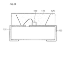
- FIG. 17 is a cross-sectional view of a light emitting device package including a light emitting device according to embodiments.
- FIG. 18 is a disassembled perspective view of a backlight unit including a light emitting device or a light emitting device package according to an embodiment.
- FIG. 19 is a perspective view of a lighting unit including a light emitting device or a light emitting device package according to an embodiment.
- a vertical type light emitting device that includes a light emitting semiconductor layer including a second conductive type semiconductor layer, an active layer and a first conductive semiconductor layer sequentially stacked, a first electrode on the light emitting semiconductor layer (i.e., on the first conductive type semiconductor layer), and a second electrode under the light emitting semiconductor layer (i.e., under the second conductive semiconductor layer).
- the second electrode may be formed under the light emitting semiconductor layer in a single layer.
- a reflective layer having a high reflectivity may be formed between the second conductive type semiconductor layer and the second electrode to thus enhance the light efficiency.
- the distance between the active layer and the semiconductor layer is very close, the distance between the active layer and the reflective layer is shorter than a wavelength of light emitted from the active layer. Therefore, by changing the distance between the active layer and the reflective layer, a quantum interference effect may be generated to change optical characteristics of the light emitting device. For example, as the distance between the active layer and the reflective layer is changed, the damping rate of a dipole source in the light emitted from the light emitting device is changed.
- FIGs. 1 and 2 are graphs describing a variation in the damping rate according to a vibration direction of a dipole source of light emitted from a light emitting device according to a variation in the distance between an active layer and a reflective layer.
- the damping rate indicates the reciprocal of time taken while electrons of the light emitting device receive energy and emit the received energy in a form of light.
- the damping rate is increased, the probability that the dipole source proceeds to a light emitting process is increased, so that the internal quantum efficiency can be enhanced.
- the damping rate of the light emitted from the light emitting device is changed depending on the gap distance D between the active layer and the reflective layer, the refractive index of a material constituting the light emitting device, and the wavelength of the light emitted from the light emitting device.
- a Y-axis indicates the damping rate
- an upper X-axis indicates the gap distance D between the active layer and the reflective layer
- a lower X-axis indicates a relative value obtained by dividing the gap distance between the active layer and the reflective layer by ⁇ /n, where ⁇ is a peak wavelength of light emitted from the light emitting device and n is a refractive index of a material constituting the light emitting device.
- the light emitting device exemplified in FIGs. 1 and 2 is a GaN-based light emitting device which emits blue light having the peak wavelength ( ⁇ ) of 450 nm and has the refractive index (n) of 2.46.
- the damping rate shows a maximum value at a specific distance (e.g., 50 nm).
- the optical characteristics may be changed with a variation in the gap distance between the active layer and the reflective layer.
- the damping rate of the dipole source vibrating vertically to the x-y plane and the damping rate of the dipole source vibrating horizontally to the x-y plane may be changed by changing the gap distance between the active layer and the reflective layer.
- a polarizer is formed between a second conductive semiconductor layer and a reflective layer to change the damping rate of the dipole source vibrating in the x direction and the damping rate of the dipole source vibrating in the y direction, so that light having a superior polarized component in a specific direction is emitted.
- FIG. 3 is a side sectional view of a light emitting device according to a first embodiment.
- the light emitting device includes a second electrode 10, a reflective layer 20 on the second electrode 10, a polarizer such as a polarization inducing pattern 80 on the reflective layer 20, an ohmic layer 25 on the reflective layer 20 and the polarization inducing pattern 80, a second conductive type semiconductor layer 30 on the ohmic layer 25, an active layer 40 on the second conductive type semiconductor layer 30, a first conductive type semiconductor layer 50 on the active layer 40, and a first electrode 70 on the first conductive type semiconductor layer 50.
- an undoped semiconductor layer 60 may be formed on the first conductive type semiconductor layer 50 and may be spaced apart from the first electrode 70.
- the second electrode 10 may be formed of copper (Cu), titanium (Ti), chromium (Cr), nickel (Ni), aluminum (Al), platinum (Pt), molybdenum (Mo), gold (Au), tungsten (W) or a semiconductor substrate (e.g., Si, Ge, GaAs, ZnO, SiC, SiGe, GaN, etc.) doped with an impurity.
- the second electrode 10 supplies electric power to the active layer 40 together with the first electrode 70.
- the reflective layer 20 may be formed on the second electrode 10.
- the reflective layer 20 may partially contact the ohmic layer 25, and may be formed of a metal or alloy having a high reflectance.
- the metal of alloy may includes at least one selected from the group comprising Ag, Al, Pd, and Pt.
- a junction metal layer (not shown) may be formed between the second electrode 10 and the reflective layer 20 so as to reinforce an interface junction force between the second electrode 10 and the reflective layer 20.
- the junction metal layer may include nickel (Ni), titanium (Ti), etc.
- the polarization inducing pattern 80 is formed on the reflective layer 20 and under the ohmic layer 25. A side surface of the polarization inducing pattern 80 may be formed such that at least some portion thereof is enclosed by the reflective layer 20.
- the polarization inducing pattern 80 may be formed of a nonmetallic material or metallic material having a refractive index which is different from that of the reflective layer 20.
- the polarization inducing pattern 80 may be formed of a nonmetallic material, such as, at least one of oxide, nitride, or fluoride.
- the polarization inducing pattern 80 may be formed of at least one of indium tin oxide (ITO), indium zinc oxide (IZO), aluminum zinc oxide (AZO), magnesium zinc oxide (MZO), gallium zinc oxide (GZO), RuO x , IrO x , ZnO, SiO 2 , MgF 2 , SOG, TiO 2 , A1 2 O 3 , or Si 3 N 4 .
- the polarization inducing pattern 80 may be formed of a metallic material different from that of the reflective layer 20, for example, may be formed of at least one of Ti, Ni, Pt, Ir, or Rh.
- the polarization inducing pattern 80 may include a plurality of protrusion patterns, which protrudes toward an inside of the reflective layer 20 in a direction (a negative Z-axis direction in the drawings) vertical to the reflective layer and spaced apart from each other.
- the invention is not limited thereto.
- the polarization inducing pattern 80 may be formed of a material having electrical conductivity and current flows through the polarization inducing pattern 80
- the polarization inducing pattern 82 may be formed on an entire surface of the reflective layer 20, as shown in FIG. 4 . That is, the polarization inducing pattern 80 may include a flat portion 82a which is a single body formed on the entire surface of the reflective layer 20 with a plurality of protrusion patterns 82b protruded toward the inside of the reflective layer 20 from the flat portion 82a.
- the polarization of the light emitted from the active layer 40 is controlled by the reflective layer 20 and the polarization inducing pattern 80. That is, the light emitted from the light emitting device has more polarized component in a specific direction than other directions.
- the polarization inducing pattern 80 is disposed at a distance shorter than the wavelength of the light emitted from the light emitting device, the light having superior polarized component in a specific direction may be emitted.
- light efficiency may be decreased.
- the foregoing light efficiency decrease can be prevented. That is, according to the embodiment, the light having superior polarized component in a specific direction may be emitted with a superior efficiency.
- the ohmic layer 25 may be formed on the reflective layer 20.
- the ohmic layer 25 may be formed on the reflective layer 20 and the polarization inducing pattern 80 as shown in FIG. 3 .
- the ohmic layer 25 forms an ohmic contact between the second electrode 10 and the second conductive type semiconductor layer 30 so that current may flow smoothly between the second electrode 10 and the second conductive type semiconductor layer 30, thereby enhancing the light emitting efficiency.
- the ohmic layer 25 may, for example, include at least one of Ni, Pt, Cr, Ti, indium tin oxide (ITO), indium zinc oxide (IZO), indium zinc tin oxide (IZTO), indium aluminum zinc oxide (IAZO), indium gallium zinc oxide (IGZO), indium gallium tin oxide (IGTO), aluminum zinc oxide (AZO), antimony tin oxide (ATO), gallium zinc oxide (GZO), IrO x , or RuO x .
- the ohmic layer 25 may be formed at a thickness ranging from 1 nm to 30 nm.
- the metallic material may have transparency to thus minimize the light being absorbed by the ohmic layer 25 and being lost.
- the ohmic layer 25 may have a thickness ranging from 10 nm to 300 nm.
- the second conductive type semiconductor layer 30 may be formed on the ohmic layer 25.
- the second conductive type semiconductor layer 30 may be, for example, implemented by a p-type semiconductor layer having a compositional formula of In x AlyGa 1-x-y N (0 ⁇ x ⁇ 1, 0 ⁇ y ⁇ 1, 0 ⁇ x+y ⁇ 1).
- the p-type semiconductor layer may be, for example, selected from InAlGaN, GaN, AIGaN, AlInN, InGaN, AIN, InN, or the like, and may be doped with a p-type dopant, such as Mg, Zn, Ca, Sr, Ba, or the like.
- the active layer 40 may be formed on the second conductive type semiconductor layer 30.
- the active layer 40 may be formed including a semiconductor material having a compositional formula of In x Al y Ga 1-x-y N (0 ⁇ x ⁇ 1,0 ⁇ y ⁇ 1, 0 ⁇ x+y ⁇ 1), and may be formed in at least one of a single quantum well structure, a multi quantum well (MQW) structure, a quantum dot structure, or a quantum-wire structure.
- MQW multi quantum well
- the active layer 40 may generate light from energy generated while electrons and holes provided from the first conductive type semiconductor layer 50 and the second conductive type semiconductor layer 30 are recombined.
- the first conductive type semiconductor layer 50 may be formed on the active layer 40.
- the first conductive type semiconductor layer 50 may, for example, include an n-type semiconductor layer having a compositional formula of In x Al y Ga 1-x-y N (0 ⁇ x ⁇ 1, 0 ⁇ y ⁇ 1, 0 ⁇ x+y ⁇ 1).
- the n-type semiconductor layer may be, for example, selected from InAIGaN, GaN, AIGaN, AlInN, InGaN, A1N, InN, or the like, and may be doped with an n-type dopant, such as Si, Ge, Sn, or the like.
- an n-type or a p-type semiconductor layer may be further formed under the second conductive type semiconductor layer 30.
- the first conductive type semiconductor layer may be implemented by a p-type semiconductor layer and the second conductive type semiconductor layer may be implemented by an n-type semiconductor layer. Therefore, the light emitting device may include at least one of np junction, pn junction, npn junction, or pnp junction structures, but the present invention is not limited thereto.
- the undoped semiconductor layer 60 may be formed on the first conductive type semiconductor layer 50.
- the undoped semiconductor layer 60 indicates a semiconductor layer having a lower electrical conductivity than the first conductive type semiconductor layer 50 and the second conductive type semiconductor layer 30.
- the undoped semiconductor layer 60 may be an undoped GaN layer.
- the first electrode 70 may be formed in a single layer or multi-layer structure including at least one of Al, Ti, Cr, Ni, Cu, or Au, and may supply power provided from an external power source to the light emitting device.
- FIG. 5 is a cross-sectional view of a light emitting device according to a second embodiment. In describing the second embodiment, the description overlapping that in the first embodiment will be omitted.
- the light emitting device includes a second electrode 10, a reflective layer 20 on the second electrode 10, an ohmic layer 25 having a protrusion pattern 84 on the reflective layer 20, a second conductive type semiconductor layer 30 on the ohmic layer 25, an active layer 40 on the second conductive type semiconductor layer 30, a first conductive type semiconductor layer 50 on the active layer 40, and a first electrode 70 on the first conductive type semiconductor layer 50.
- an undoped semiconductor layer 60 may be formed on the first conductive type semiconductor layer 50.
- the protrusion pattern 84 formed integrally with the ohmic layer 25 forms a polarization inducing pattern. That is, in this embodiment, the protrusion pattern 84 is formed integrally with the ohmic layer 25 such that the ohmic layer 25 may function not only as a layer for ohmic contact but also as a polarization inducing pattern.
- the protrusion patterns 84 protrude toward the reflective layer 20, and may be spaced apart by a predetermined distance from each other. That is, the protrusion patterns 84 are formed such that lower surfaces and side surfaces thereof protrude toward the inside of the reflective layer 20.
- the protrusion pattern 84 may be, for example, formed by forming the ohmic layer 25 and selectively etching the ohmic layer 25, but the invention is not limited thereto.
- FIG. 6 is a cross-sectional view of a light emitting device according to a third embodiment. In describing the third embodiment, the description overlapping that in the first embodiment will be omitted.
- the light emitting device includes a second electrode 10, a reflective layer 20 on the second electrode 10, a polarization inducing pattern 80 on the reflective layer 20, an ohmic layer 25 on the reflective layer 20 and the polarization inducing pattern 80, a second conductive type semiconductor layer 30 on the ohmic layer 25, an active layer 40 on the second conductive type semiconductor layer 30, a first conductive type semiconductor layer 50 on the active layer 40, a first electrode 70 on the first conductive type semiconductor layer 50, and an undoped semiconductor layer 60 on the first conductive type semiconductor layer 50.
- the undoped semiconductor layer 60 may have a pillar-shaped or hole-shaped photonic crystal structure 63.
- holes 61 are formed in the undoped semiconductor layer 60.
- the pillar or holes 61 are arranged with a period ranging from 50 nm to 3000 nm to selectively transmit or reflect light having a predetermined wavelength band, thereby enhancing light extraction efficiency.
- the undoped semiconductor layer 60 may have a random roughness formed by wet etching, but the invention is not limited thereto.
- FIG. 6 exemplarily shows the light emitting device provided with the polarization inducing pattern 80 of FIG. 3
- the photonic crystal structure 63 may be formed at an upper portion of the undoped semiconductor layer 60 of the light emitting device shown in FIGs. 4 and 5 .
- FIG. 7 is a cross-sectional view of a light emitting device according to a fourth embodiment.
- the description overlapping that in the first embodiment will be omitted.
- the light emitting device includes a second electrode 10, a reflective layer 20 on the second electrode 10, a polarization inducing pattern 80 on the reflective layer 20, an ohmic layer 25 on the reflective layer 20 and the polarization inducing pattern 80, a current blocking layer 28 on the ohmic layer 25, a second conductive type semiconductor layer 30 on the ohmic layer 25 and the current blocking layer 28, an active layer 40 on the second conductive type semiconductor layer 30, a first conductive type semiconductor layer 50 on the active layer 40, a first electrode 70 on the first conductive type semiconductor layer 50, and an undoped semiconductor layer 60 on the first conductive type semiconductor layer 50.
- the current blocking layer 28 may be formed between the ohmic layer 25 and the second conductive type semiconductor layer 30 such that the current blocking layer 28 partially overlaps the first electrode 70 in a vertical direction. Therefore, the current blocking layer 28 can prevent current from being concentrated along the shortest path so that the current is distributed into the entire region of the light emitting device, thereby contributing to the enhancement in the light emitting efficiency.
- the current blocking layer 28 may be formed of a material forming a Shottkey contact with the second conductive type semiconductor layer 30, a material having an electrical insulation property, or a material having an electrical conductivity lower than the ohmic layer 25.
- the current blocking layer 28 may include at least one of ZnO, SiO 2 , SiO x , SiO x N y , Si 3 N 4 , A1 2 O 3 , TiO x , Ti, Al, or Cr, but the invention is not limited thereto.
- FIGs. 8 to 10 are plan views exemplarily illustrating polarization inducing patterns in light emitting devices according to embodiments.
- the polarization inducing patterns 80, 86, 88 shown respectively in FIGs. 8 to 10 are shapes on the x-y plane as viewed from a top side.
- the polarization inducing patterns 80, 86, 88 shown respectively in FIGs. 8 to 10 are only one example, and the embodiments are not limited thereto.
- FIGs. 8 to 10 exemplarily show that the polarization inducing patterns 80, 86, 88 spaced apart from one another are formed on the reflective layer 20.
- the protrusion pattern 82a of FIG. 4 or the protrusion pattern 84 of FIG. 5 may have the shapes shown in FIGs. 8 to 10 .
- polarization inducing pattern 80, 86, 88 is exchanged with the pattern of the reflective layer 20 may be also included in this embodiment.
- the polarization inducing pattern 80 is formed in a line shape on the reflective layer 20.
- the polarization inducing pattern 80 is formed in plurality in a line shape in a first direction, and the plurality of polarization inducing patterns 80 are spaced apart from one another.
- the polarization inducing patterns 80 extend in the first direction, and are disposed spaced apart from one another in a second direction perpendicular to the first direction.
- the polarization inducing pattern 80 has a line shape extending in a y-axis direction, and is formed in plurality.
- the plurality of polarization inducing patterns 80 are spaced apart from one another in x-axis direction. Therefore, the polarization inducing pattern 80 may have a stripe shape.
- the polarization inducing pattern 86 of which the length in the x-axis direction is different from the length in the y-axis direction is formed on the reflective layer.
- the polarization inducing pattern 86 is formed such that the length r y in the y-axis direction is greater than the length r x in the x-axis direction. As shown in FIG. 9 , while the polarization inducing pattern 86 may be formed in an elliptical shape of which the length in the y-axis direction is greater than the length in the x-axis direction, the invention is not limited thereto.
- the polarization inducing patterns 88 are arranged on the reflective layer 20 such that the distance in a first direction is different from the distance in a second direction perpendicular to the first direction.
- the polarization inducing pattern 88 is formed in a circular shape, and the distance a x thereof in the x-axis direction may be less than the distance a y thereof in the y-axis direction.
- the polarization inducing pattern 88 may have a polygonal shape, such as a triangle, a rectangle, or the like.
- the polarization inducing patterns 80, 86, 88 shown in FIGs. 8 to 10 may be formed with a constant regularity in the first and second directions, and the regularity in the first direction may be different from the regularity in the second direction.
- FIGs. 11 to 16 are cross-sectional views illustrating a method of manufacturing a light emitting device according to the first embodiment.
- an undoped semiconductor layer 60, a first conductive type semiconductor layer 50, an active layer 40 and a second conductive type semiconductor layer 30 may be sequentially grown and formed on a growth substrate 15.
- the growth substrate 15 may be formed of at least one of sapphire (A1 2 O 3 ), SiC, GaAs, GaN, ZnO, Si, GaP, InP, or Ge, but the invention is not limited thereto.
- the growth substrate 15 may be formed by a method such as a metal organic chemical vapor deposition (MOCVD), a chemical vapor deposition (CVD), a plasma-enhanced chemical vapor deposition (PECVD), a molecular beam epitaxy (MBE), a hydride vapor phase epitaxy (HVPE), or the like, but the invention is not limited thereto.
- MOCVD metal organic chemical vapor deposition
- CVD chemical vapor deposition
- PECVD plasma-enhanced chemical vapor deposition
- MBE molecular beam epitaxy
- HVPE hydride vapor phase epitaxy
- a buffer layer (not shown) may be further formed between the first conductive type semiconductor layer 50 and the growth substrate 15 so as to buffer a difference in the lattice constant therebetween.
- an ohmic layer 25 may be formed on the second conductive type semiconductor layer 30.
- the ohmic layer 25 may be, for example, formed by a deposition method, such as a plasma enhanced chemical vapor deposition (PECVD), an electron beam deposition, a sputtering, or the like.
- PECVD plasma enhanced chemical vapor deposition
- electron beam deposition a sputtering, or the like.
- a polarization inducing pattern 80 may be formed on the ohmic layer 25.
- the polarization inducing pattern 80 may be formed by using a photolithography process or a deposition method.
- the polarization inducing pattern 80 may be formed by forming a metallic layer or a nonmetallic layer and selectively removing the metal layer or the nonmetallic layer through an etch process.
- the polarization inducing pattern 80 may be formed by forming a pattern mask corresponding to the polarization inducing pattern 80, aligning the pattern mask on the ohmic layer 25 and performing deposition.
- the polarization inducing pattern 80 may be formed by forming a metallic layer or a nonmetallic layer and patterning the metal layer or nonmetallic layer have a rough surface layer through wet etching.
- a reflective layer 20 may be formed on the ohmic layer 25 and the polarization inducing pattern 80, and a second electrode 10 may be formed on the reflective layer 20.
- the reflective layer 20 may be formed by plating or deposition.
- the reflective layer 20 may be formed by plating or deposition, but may be formed by preparing the second electrode in a sheet shape and bonding the prepared second electrode on the reflective layer 20.
- junction metal layer (not shown) may be further formed between the second electrode 10 and the reflective layer 20 so as to enhance an interfacial adhesive force.
- the growth substrate 15 may be removed.
- the growth substrate 15 may be, for example, removed by using a laser lift off process or an etching process.
- an etch process is performed such that the upper surface of the first conductive type semiconductor layer 50 is at least partially exposed, and then a first electrode 70 is formed on the exposed first conductive type semiconductor layer 50, so that the light emitting device according to the first embodiment can be provided.
- FIG. 17 is a cross-sectional view of a light emitting device package including a light emitting device according to embodiments.
- the light emitting device package includes a body 120, first and second electrode layers 131 and 132 mounted on the body 120, a light emitting device 100 according to the embodiments, which is mounted on the body 120 and electrically connected to the first and second electrode layers 131 and 132, and a molding member 140 enclosing the light emitting device 100.
- the body 120 may be formed including a silicon material, a synthetic resin material, or a metallic material, and may have an inclined surface around the light emitting device 100.
- the first electrode layer 131 and the second electrode layer 132 are electrically separated, and supply electric power to the light emitting device 100. Also, the first and second electrode layers 131 and 132 may reflect light generated from the light emitting device 100 to thus increase light efficiency, and may emit heat generated from the light emitting device 100 to an outside.
- the light emitting device 100 may be mounted on the body 120 or on the first electrode layer 131 or the second electrode layer 132.
- the light emitting device 100 may be electrically connected to the first electrode layer 131 and the second electrode layer 132 by using any one of a wire bonding method, a flip chip method, or a die bonding method.
- the molding member 140 may enclose and protect the light emitting device 100. Also, a fluorescent material may be included in the molding member 140 to change the wavelength of light emitted from the light emitting device 100.
- the light emitting device package may mount at least one of the light emitting devices according to the foregoing embodiments, but the present invention is not limited thereto.
- the light emitting device package may include a plurality of light emitting device packages which are arrayed on a substrate.
- a plurality of optical members such as a light guide panel, a prism sheet, a diffusion sheet, a fluorescent sheet, and the like may be arranged on a path of light emitted from the light emitting device package.
- the light emitting device package, substrate and optical members may function as a backlight unit or lighting unit, and a lighting system may include, for example, a backlight unit, a lighting unit, an indicator unit, a lamp, a streetlamp, etc.
- FIG. 18 is a disassembled perspective view of a backlight unit including a light emitting device or a light emitting device package according to an embodiment.
- the backlight unit 1100 of FIG. 18 is one example of lighting systems, and the present invention is not limited thereto.
- the backlight unit 1100 may include a bottom cover 1140, a light guide member 1120 disposed in the bottom cover 1140, and a light emitting module 1110 disposed on at least one side surface of the light guide member 1120 or under the light guide member 1120. Also, a reflective sheet 1130 may be disposed under the light guide member 1120.
- the bottom cover 1140 may be formed in a box shape a top surface of which is opened such that the light guide member 1120, the light emitting module 1110 and the reflective sheet 1130 can be received.
- the bottom cover 1140 may be formed of a metal or resin material, but the invention is not limited thereto.
- the light emitting module 1110 may include a substrate 700 and a plurality of light emitting device packages 600 mounted on the substrate 700.
- the plurality of light emitting device packages 600 may provide light to the light guide member 1120.
- the light emitting module 1110 according to the current embodiment it is exemplarily shown that the light emitting device packages 600 are mounted on the substrate 700, but the light emitting devices according to the embodiments may be mounted directly on the substrate 700.
- the light emitting module 1110 may be disposed on at least one of inner side surfaces of the bottom cover 1140, and thus may provide light to at least one of the side surfaces of the light guide member 1120.
- the light emitting module 1110 may be disposed under the light guide member 1120 inside the bottom cover 1140 to provide light toward a bottom surface of the light guide member 1120.
- the invention is not limited thereto.
- the light guide member 1120 may be disposed inside the bottom cover 1140.
- the light guide member 1120 may convert the light provided from the light emitting module to a planar light source and guide the converted plane light source to a display panel (not shown).
- the light guide member 1120 may be, for example, a light guide panel (LGP).
- LGP may be formed of, for example, one of acryl-series resin such as polymethyl metaacrylate (PMMA), polyethylene terephthlate (PET), poly carbonate (PC), COC, and polyethylene naphthalate resin.
- PMMA polymethyl metaacrylate
- PET polyethylene terephthlate
- PC poly carbonate
- COC polyethylene naphthalate resin
- An optical sheet 1150 may be disposed on the light guide member 1120.
- the optical sheet 1150 may include, for example, at least one of a diffusion sheet, a light-condensing sheet, a brightness enhancement sheet and a fluorescent sheet.
- the optical sheet 1150 may be configured by the diffusion sheet, the light-condensing sheet, the brightness enhancement sheet and the fluorescent sheet stacked.
- the diffusion sheet 1150 diffuses the light emitted from the light emitting module 1110 uniformly, and the diffused light may be condensed on the display panel (not shown) by the light-condensing sheet.
- the light emitted from the light-condensing sheet is a randomly polarized light
- the brightness enhancement sheet may increase the polarization of the light emitted from the light-condensing sheet.
- the light-condensing sheet may be, for example, a horizontal and/or vertical prism sheet.
- the brightness enhancement sheet may be, for example, a dual brightness enhancement film.
- the fluorescent sheet may be a transparent plate or film including a fluorescent material.
- the reflective sheet 1130 may be disposed under the light guide member 1120.
- the reflective sheet 1130 may reflect light emitted from the bottom surface of the light guide member 1120 toward a light emitting surface of the light guide member 1120.
- the reflective sheet 1130 may be formed of resin material having good reflectivity, for example, PET, PC, PVC resins, or the like, but the invention is not limited thereto.
- FIG. 19 is a perspective view of a lighting unit including the light emitting device or light emitting device package according to the embodiment.
- the lighting unit 1200 of FIG. 19 is an example of lighting systems and the invention is not limited thereto.
- the lighting unit 1200 may include a case body 1210, a light emitting module 1230 installed in the case body 1210, and a connection terminal installed in the case body 1210 to be supplied with electric power from an external power source.
- the case body 1210 may be preferably formed of a material having good heat shielding characteristic, for example, a metal material or a resin material.
- the light emitting module 1230 may include a substrate 700, and a light emitting device package 600 mounted on the substrate 700.
- a light emitting device package 600 mounted on the substrate 700, but the light emitting devices according to the embodiments may be mounted directly on the substrate 700.
- the substrate 700 may be an insulator substrate on which a circuit pattern is printed, and may include, for example, a general printed circuit board (PCB), a metal core PCB, a flexible PCB, a ceramic PCB, etc.
- PCB general printed circuit board
- metal core PCB metal core PCB
- flexible PCB flexible PCB
- ceramic PCB ceramic PCB
- the substrate 700 may be formed of a material to efficiently reflect light, and a surface thereof may be formed in a color capable of efficiently reflecting light, for example, white color, silver color, or the like.
- At least one light emitting device package may be mounted on the substrate 700.
- Each of the light emitting device packages 200 may include at least one light emitting diode (LED).
- the light emitting diode may include a color LED emitting red, green, blue or white light, and a UV LED emitting ultraviolet (UV).
- the light emitting module 1230 may have a combination of several LEDs so as to obtain desired color and luminance.
- the light emitting module 1234 may have a combination of a white LED, a red LED, and a green LED so as to obtain a high color rendering index (CRI).
- a fluorescent sheet may be further disposed on a path of light emitted from the light emitting module 1230.
- the fluorescent sheet converts the wavelength of the light emitted from the light emitting module.
- the fluorescent sheet may include a yellow fluorescent material, so that the light, which is emitted from the light emitting module 1230 and passes through the fluorescent sheet, finally appears as white light.
- connection terminal 1220 may be electrically connected to the light emitting module 1230 to supply an electric power to the light emitting module 1230. As shown in FIG. 19 , the connection terminal 1220 may be screwed and coupled to an external power, but the invention is not limited thereto. For example, the connection terminal 1220 may be made in a pin type and inserted into an external power, or may be connected to the external power through a power line.
- the lighting system may include at least one of a light guide member, a diffusion sheet, a light-condensing sheet, a brightness enhancement sheet and a fluorescent sheet on a traveling path of light to obtain a desired optical effect.
- the lighting system since the lighting system according to this embodiment includes the light emitting device or light emitting device package capable of emitting light having a superior polarized component in a specific direction at a superior efficiency, the lighting system can show superior characteristics. Also, while several embodiments were described with reference to the reflective layer, the polarization inducing pattern may be on any suitable layer near the active layer where a distance between the active layer and the suitable layer is shorter than a wavelength of light emitted from the active layer.
- any reference in this specification to "one embodiment,” “an embodiment,” “example embodiment,” etc. means that a particular feature, structure, or characteristic described in connection with the embodiment is included in at least one embodiment of the invention.
- the appearances of such phrases in various places in the specification are not necessarily all referring to the same embodiment.
Landscapes
- Engineering & Computer Science (AREA)
- Manufacturing & Machinery (AREA)
- Computer Hardware Design (AREA)
- Microelectronics & Electronic Packaging (AREA)
- Power Engineering (AREA)
- Led Devices (AREA)
- Led Device Packages (AREA)
Applications Claiming Priority (1)
| Application Number | Priority Date | Filing Date | Title |
|---|---|---|---|
| KR1020100014440A KR101667815B1 (ko) | 2010-02-18 | 2010-02-18 | 발광 소자, 발광 소자 제조방법 및 발광 소자 패키지 |
Publications (2)
| Publication Number | Publication Date |
|---|---|
| EP2362448A1 true EP2362448A1 (fr) | 2011-08-31 |
| EP2362448B1 EP2362448B1 (fr) | 2014-07-02 |
Family
ID=43416397
Family Applications (1)
| Application Number | Title | Priority Date | Filing Date |
|---|---|---|---|
| EP20100188775 Active EP2362448B1 (fr) | 2010-02-18 | 2010-10-25 | Dispositif électroluminescent, son procédé de fabrication, conditionnement de dispositif électroluminescent et système d'éclairage |
Country Status (6)
| Country | Link |
|---|---|
| US (1) | US8384094B2 (fr) |
| EP (1) | EP2362448B1 (fr) |
| JP (1) | JP5479384B2 (fr) |
| KR (1) | KR101667815B1 (fr) |
| CN (1) | CN102163674B (fr) |
| TW (1) | TWI413280B (fr) |
Cited By (3)
| Publication number | Priority date | Publication date | Assignee | Title |
|---|---|---|---|---|
| EP2360747A2 (fr) * | 2010-02-23 | 2011-08-24 | LG Innotek Co., Ltd. | Dispositif électroluminescent, paquet de dispositif électroluminescent, procédé de fabrication de dispositif électroluminescent et système d'éclairage |
| FR3105586A1 (fr) * | 2019-12-23 | 2021-06-25 | Commissariat à l'Energie Atomique et aux Energies Alternatives | Procédé de fabrication d’une diode électroluminescente comportant une étape de dimensionnement d’une couche semiconductrice |
| FR3105587A1 (fr) * | 2019-12-23 | 2021-06-25 | Commissariat à l'Energie Atomique et aux Energies Alternatives | Procédé de fabrication d’une diode électroluminescente a couche d’extraction comportant une étape de dimensionnement d’une couche semiconductrice |
Families Citing this family (12)
| Publication number | Priority date | Publication date | Assignee | Title |
|---|---|---|---|---|
| DE102011017196A1 (de) * | 2011-04-15 | 2012-10-18 | Osram Opto Semiconductors Gmbh | Polarisierte Strahlung emittierender Halbleiterchip |
| JP2014049603A (ja) * | 2012-08-31 | 2014-03-17 | Toshiba Corp | 半導体発光装置 |
| WO2014175564A1 (fr) * | 2013-04-22 | 2014-10-30 | 한국산업기술대학교산학협력단 | Procédé de fabrication d'une diode électroluminescente de type vertical, diode électroluminescente de type vertical, procédé de fabrication d'une diode électroluminescente à rayonnement ultraviolet, et diode électroluminescente à rayonnement ultraviolet |
| KR101506961B1 (ko) * | 2013-05-06 | 2015-03-30 | 한국산업기술대학교산학협력단 | 수직형 발광다이오드 제조 방법 및 수직형 발광다이오드 |
| CN110047865B (zh) * | 2013-09-03 | 2024-02-23 | 晶元光电股份有限公司 | 具有多个发光结构的发光元件 |
| KR101615564B1 (ko) * | 2015-02-23 | 2016-04-28 | 한국산업기술대학교산학협력단 | 수직형 발광다이오드 제조 방법 및 수직형 발광다이오드 |
| CN104635991B (zh) * | 2015-03-11 | 2019-01-11 | 合肥鑫晟光电科技有限公司 | 一种消影结构、触摸屏及其制备方法 |
| US10892381B2 (en) * | 2018-02-28 | 2021-01-12 | Sensor Electronic Technology, Inc. | Semiconductor structure with layer having protrusions |
| KR20200076969A (ko) * | 2018-12-20 | 2020-06-30 | 엘지디스플레이 주식회사 | 유기 발광 소자를 이용한 조명 장치 |
| JP2020108087A (ja) * | 2018-12-28 | 2020-07-09 | セイコーエプソン株式会社 | 振動デバイス、電子機器および移動体 |
| US11949043B2 (en) | 2020-10-29 | 2024-04-02 | PlayNitride Display Co., Ltd. | Micro light-emitting diode |
| TWI779378B (zh) * | 2020-10-29 | 2022-10-01 | 錼創顯示科技股份有限公司 | 微型發光二極體 |
Citations (5)
| Publication number | Priority date | Publication date | Assignee | Title |
|---|---|---|---|---|
| US20050087884A1 (en) * | 2003-10-24 | 2005-04-28 | Stokes Edward B. | Flip-chip light emitting diode |
| US20050151145A1 (en) * | 2004-01-08 | 2005-07-14 | Chung-Hsiang Lin | Light emitting device with a photonic crystal |
| US20080054283A1 (en) * | 2006-08-30 | 2008-03-06 | Samsung Electronics Co., Ltd. | Polarized light emitting diode and method of forming the same |
| DE102007059621A1 (de) * | 2007-09-28 | 2009-04-02 | Osram Opto Semiconductors Gmbh | Verfahren zum Erzeugen von linear polarisiertem Licht und strahlungsemittierende Bauelemente |
| US20090128004A1 (en) * | 2007-11-21 | 2009-05-21 | Industrial Technology Research Institute | Light-emitting device |
Family Cites Families (14)
| Publication number | Priority date | Publication date | Assignee | Title |
|---|---|---|---|---|
| JP2961964B2 (ja) * | 1991-07-10 | 1999-10-12 | 日本電気株式会社 | 半導体レーザ装置 |
| JP3541539B2 (ja) * | 1996-02-01 | 2004-07-14 | 富士通株式会社 | 面発光半導体レーザ |
| JP4824270B2 (ja) * | 2003-09-29 | 2011-11-30 | 浜松ホトニクス株式会社 | 半導体基板 |
| US7808011B2 (en) | 2004-03-19 | 2010-10-05 | Koninklijke Philips Electronics N.V. | Semiconductor light emitting devices including in-plane light emitting layers |
| TWI244228B (en) * | 2005-02-03 | 2005-11-21 | United Epitaxy Co Ltd | Light emitting device and manufacture method thereof |
| JP4589805B2 (ja) * | 2005-05-23 | 2010-12-01 | 株式会社リコー | 偏光制御素子 |
| JP2007109689A (ja) * | 2005-10-11 | 2007-04-26 | Seiko Epson Corp | 発光素子、発光素子の製造方法及び画像表示装置 |
| KR101229834B1 (ko) * | 2006-09-25 | 2013-02-04 | 서울옵토디바이스주식회사 | 수직형 발광 다이오드 및 그 제조방법 |
| KR101337617B1 (ko) | 2006-11-08 | 2013-12-06 | 서울바이오시스 주식회사 | 오믹 전극 패턴을 갖는 수직형 발광 다이오드 및 그제조방법 |
| JP2008283028A (ja) * | 2007-05-11 | 2008-11-20 | Fuji Xerox Co Ltd | 面発光型半導体レーザ、面発光型半導体レーザの製造方法、モジュール、光源装置、情報処理装置、光送信装置、光空間伝送装置および光空間伝送システム。 |
| DE102007060202A1 (de) | 2007-12-14 | 2009-06-25 | Osram Opto Semiconductors Gmbh | Polarisierte Strahlung emittierendes Halbleiterbauelement |
| TWI370560B (en) * | 2007-12-14 | 2012-08-11 | Delta Electronics Inc | Light-emitting diode device and manufacturing method thereof |
| JP5206029B2 (ja) * | 2008-03-04 | 2013-06-12 | ソニー株式会社 | 液晶表示装置 |
| KR101007099B1 (ko) * | 2008-04-21 | 2011-01-10 | 엘지이노텍 주식회사 | 반도체 발광소자 및 그 제조방법 |
-
2010
- 2010-02-18 KR KR1020100014440A patent/KR101667815B1/ko active IP Right Grant
- 2010-10-25 EP EP20100188775 patent/EP2362448B1/fr active Active
- 2010-11-17 TW TW99139530A patent/TWI413280B/zh active
- 2010-11-24 US US12/954,153 patent/US8384094B2/en active Active
- 2010-12-29 CN CN201010621719.9A patent/CN102163674B/zh not_active Expired - Fee Related
-
2011
- 2011-02-18 JP JP2011032766A patent/JP5479384B2/ja not_active Expired - Fee Related
Patent Citations (5)
| Publication number | Priority date | Publication date | Assignee | Title |
|---|---|---|---|---|
| US20050087884A1 (en) * | 2003-10-24 | 2005-04-28 | Stokes Edward B. | Flip-chip light emitting diode |
| US20050151145A1 (en) * | 2004-01-08 | 2005-07-14 | Chung-Hsiang Lin | Light emitting device with a photonic crystal |
| US20080054283A1 (en) * | 2006-08-30 | 2008-03-06 | Samsung Electronics Co., Ltd. | Polarized light emitting diode and method of forming the same |
| DE102007059621A1 (de) * | 2007-09-28 | 2009-04-02 | Osram Opto Semiconductors Gmbh | Verfahren zum Erzeugen von linear polarisiertem Licht und strahlungsemittierende Bauelemente |
| US20090128004A1 (en) * | 2007-11-21 | 2009-05-21 | Industrial Technology Research Institute | Light-emitting device |
Non-Patent Citations (1)
| Title |
|---|
| JUNG M R ET AL: "Theoretical analysis of polarization characteristics of InGaN/GaN LEDs with photonic crystals", NUMERICAL SIMULATION OF OPTOELECTRONIC DEVICES, 2009. NUSOD 2009. 9TH INTERNATIONAL CONFERENCE ON, IEEE, PISCATAWAY, NJ, USA, 14 September 2009 (2009-09-14), pages 25 - 26, XP031551971, ISBN: 978-1-4244-4180-8 * |
Cited By (7)
| Publication number | Priority date | Publication date | Assignee | Title |
|---|---|---|---|---|
| EP2360747A2 (fr) * | 2010-02-23 | 2011-08-24 | LG Innotek Co., Ltd. | Dispositif électroluminescent, paquet de dispositif électroluminescent, procédé de fabrication de dispositif électroluminescent et système d'éclairage |
| FR3105586A1 (fr) * | 2019-12-23 | 2021-06-25 | Commissariat à l'Energie Atomique et aux Energies Alternatives | Procédé de fabrication d’une diode électroluminescente comportant une étape de dimensionnement d’une couche semiconductrice |
| FR3105587A1 (fr) * | 2019-12-23 | 2021-06-25 | Commissariat à l'Energie Atomique et aux Energies Alternatives | Procédé de fabrication d’une diode électroluminescente a couche d’extraction comportant une étape de dimensionnement d’une couche semiconductrice |
| EP3843162A1 (fr) * | 2019-12-23 | 2021-06-30 | Commissariat à l'Energie Atomique et aux Energies Alternatives | Procede de fabrication d'une diode electroluminescente a couche d'extraction comportant une etape de dimensionnement d'une couche semiconductrice |
| EP3843161A1 (fr) * | 2019-12-23 | 2021-06-30 | Commissariat à l'Energie Atomique et aux Energies Alternatives | Procede de fabrication d'une diode electroluminescente comportant une etape de dimensionnement d'une couche semiconductrice |
| US11430972B2 (en) | 2019-12-23 | 2022-08-30 | Commissariat A L'energie Atomique Et Aux Energies Alternatives | Method for producing a light-emitting diode comprising a step of dimensioning a semiconductor layer |
| US11482652B2 (en) | 2019-12-23 | 2022-10-25 | Commissariat A L'energie Atomique Et Aux Energies Alternatives | Method for producing an extraction-layer light-emitting diode comprising a step of dimensioning a semiconductor layer |
Also Published As
| Publication number | Publication date |
|---|---|
| JP2011171738A (ja) | 2011-09-01 |
| CN102163674B (zh) | 2014-09-10 |
| US20110198642A1 (en) | 2011-08-18 |
| KR20110094810A (ko) | 2011-08-24 |
| CN102163674A (zh) | 2011-08-24 |
| KR101667815B1 (ko) | 2016-10-19 |
| EP2362448B1 (fr) | 2014-07-02 |
| TW201130159A (en) | 2011-09-01 |
| US8384094B2 (en) | 2013-02-26 |
| JP5479384B2 (ja) | 2014-04-23 |
| TWI413280B (zh) | 2013-10-21 |
Similar Documents
| Publication | Publication Date | Title |
|---|---|---|
| EP2362448B1 (fr) | Dispositif électroluminescent, son procédé de fabrication, conditionnement de dispositif électroluminescent et système d'éclairage | |
| EP2432036B1 (fr) | Diode électroluminescente | |
| EP2333852B1 (fr) | Dispositif électroluminescent et paquet électroluminescent | |
| EP2402995B1 (fr) | Dispositif électroluminescent et unité d'éclairage | |
| EP2323181B1 (fr) | Dispositif électroluminescent et emballage de dispositif électroluminescent | |
| EP2378573B1 (fr) | Diode électroluminescente et boîtier de diode électroluminescente | |
| US9537056B2 (en) | Light emitting device | |
| KR101154709B1 (ko) | 발광 소자, 발광 소자 제조방법, 발광 소자 패키지 및 조명 시스템 | |
| US8916891B2 (en) | Light emitting device, light emitting device package, method of manufacturing light emitting device, and lighting system | |
| US8368107B2 (en) | Light emitting device, method of manufacturing the same, and light emitting device package | |
| US9595647B2 (en) | Light emitting device and light emitting device package | |
| US8686456B2 (en) | Light emitting device, light emitting device package, and light unit | |
| US20120299047A1 (en) | Light emitting device, light emitting device package, and light unit | |
| KR101803569B1 (ko) | 발광 소자 | |
| EP2369644A2 (fr) | Diode électroluminescente, son procédé de fabrication, boîtier pour diode électroluminescente et système d'éclairage l'incorporant | |
| US8350274B2 (en) | Light emitting device, method of manufacturing the light emitting device, light emitting device package, and lighting unit | |
| EP2390934A2 (fr) | Dispositif électroluminescent et emballage du dispositif électroluminescent | |
| KR20110115384A (ko) | 발광 소자 및 그 제조방법, 발광 소자 패키지 및 조명 시스템 | |
| KR20120020599A (ko) | 발광 소자 및 발광 소자 패키지 | |
| KR20120029868A (ko) | 발광 소자, 발광 소자 패키지 및 조명 시스템 | |
| KR20120022091A (ko) | 발광 소자, 발광 소자 제조방법, 발광 소자 패키지 및 조명 시스템 | |
| KR20120015882A (ko) | 발광소자 패키지 | |
| KR20120038338A (ko) | 발광 소자, 발광 소자 제조방법, 발광 소자 패키지 및 조명 시스템 | |
| KR20120052789A (ko) | 발광 소자 | |
| KR20120088046A (ko) | 발광 소자, 발광 소자 패키지 및 조명 시스템 |
Legal Events
| Date | Code | Title | Description |
|---|---|---|---|
| PUAI | Public reference made under article 153(3) epc to a published international application that has entered the european phase |
Free format text: ORIGINAL CODE: 0009012 |
|
| 17P | Request for examination filed |
Effective date: 20101025 |
|
| AK | Designated contracting states |
Kind code of ref document: A1 Designated state(s): AL AT BE BG CH CY CZ DE DK EE ES FI FR GB GR HR HU IE IS IT LI LT LU LV MC MK MT NL NO PL PT RO RS SE SI SK SM TR |
|
| AX | Request for extension of the european patent |
Extension state: BA ME |
|
| 17Q | First examination report despatched |
Effective date: 20120614 |
|
| GRAP | Despatch of communication of intention to grant a patent |
Free format text: ORIGINAL CODE: EPIDOSNIGR1 |
|
| INTG | Intention to grant announced |
Effective date: 20140116 |
|
| GRAS | Grant fee paid |
Free format text: ORIGINAL CODE: EPIDOSNIGR3 |
|
| GRAA | (expected) grant |
Free format text: ORIGINAL CODE: 0009210 |
|
| RAP1 | Party data changed (applicant data changed or rights of an application transferred) |
Owner name: LG INNOTEK CO., LTD. |
|
| AK | Designated contracting states |
Kind code of ref document: B1 Designated state(s): AL AT BE BG CH CY CZ DE DK EE ES FI FR GB GR HR HU IE IS IT LI LT LU LV MC MK MT NL NO PL PT RO RS SE SI SK SM TR |
|
| REG | Reference to a national code |
Ref country code: GB Ref legal event code: FG4D |
|
| REG | Reference to a national code |
Ref country code: CH Ref legal event code: EP |
|
| REG | Reference to a national code |
Ref country code: IE Ref legal event code: FG4D |
|
| REG | Reference to a national code |
Ref country code: DE Ref legal event code: R096 Ref document number: 602010017173 Country of ref document: DE Effective date: 20140814 |
|
| REG | Reference to a national code |
Ref country code: NL Ref legal event code: T3 |
|
| REG | Reference to a national code |
Ref country code: LT Ref legal event code: MG4D |
|
| PG25 | Lapsed in a contracting state [announced via postgrant information from national office to epo] |
Ref country code: PT Free format text: LAPSE BECAUSE OF FAILURE TO SUBMIT A TRANSLATION OF THE DESCRIPTION OR TO PAY THE FEE WITHIN THE PRESCRIBED TIME-LIMIT Effective date: 20141103 Ref country code: LT Free format text: LAPSE BECAUSE OF FAILURE TO SUBMIT A TRANSLATION OF THE DESCRIPTION OR TO PAY THE FEE WITHIN THE PRESCRIBED TIME-LIMIT Effective date: 20140702 Ref country code: FI Free format text: LAPSE BECAUSE OF FAILURE TO SUBMIT A TRANSLATION OF THE DESCRIPTION OR TO PAY THE FEE WITHIN THE PRESCRIBED TIME-LIMIT Effective date: 20140702 Ref country code: BG Free format text: LAPSE BECAUSE OF FAILURE TO SUBMIT A TRANSLATION OF THE DESCRIPTION OR TO PAY THE FEE WITHIN THE PRESCRIBED TIME-LIMIT Effective date: 20141002 Ref country code: SE Free format text: LAPSE BECAUSE OF FAILURE TO SUBMIT A TRANSLATION OF THE DESCRIPTION OR TO PAY THE FEE WITHIN THE PRESCRIBED TIME-LIMIT Effective date: 20140702 Ref country code: ES Free format text: LAPSE BECAUSE OF FAILURE TO SUBMIT A TRANSLATION OF THE DESCRIPTION OR TO PAY THE FEE WITHIN THE PRESCRIBED TIME-LIMIT Effective date: 20140702 Ref country code: NO Free format text: LAPSE BECAUSE OF FAILURE TO SUBMIT A TRANSLATION OF THE DESCRIPTION OR TO PAY THE FEE WITHIN THE PRESCRIBED TIME-LIMIT Effective date: 20141002 Ref country code: GR Free format text: LAPSE BECAUSE OF FAILURE TO SUBMIT A TRANSLATION OF THE DESCRIPTION OR TO PAY THE FEE WITHIN THE PRESCRIBED TIME-LIMIT Effective date: 20141003 Ref country code: CZ Free format text: LAPSE BECAUSE OF FAILURE TO SUBMIT A TRANSLATION OF THE DESCRIPTION OR TO PAY THE FEE WITHIN THE PRESCRIBED TIME-LIMIT Effective date: 20140702 |
|
| PG25 | Lapsed in a contracting state [announced via postgrant information from national office to epo] |
Ref country code: RS Free format text: LAPSE BECAUSE OF FAILURE TO SUBMIT A TRANSLATION OF THE DESCRIPTION OR TO PAY THE FEE WITHIN THE PRESCRIBED TIME-LIMIT Effective date: 20140702 Ref country code: IS Free format text: LAPSE BECAUSE OF FAILURE TO SUBMIT A TRANSLATION OF THE DESCRIPTION OR TO PAY THE FEE WITHIN THE PRESCRIBED TIME-LIMIT Effective date: 20141102 Ref country code: LV Free format text: LAPSE BECAUSE OF FAILURE TO SUBMIT A TRANSLATION OF THE DESCRIPTION OR TO PAY THE FEE WITHIN THE PRESCRIBED TIME-LIMIT Effective date: 20140702 Ref country code: PL Free format text: LAPSE BECAUSE OF FAILURE TO SUBMIT A TRANSLATION OF THE DESCRIPTION OR TO PAY THE FEE WITHIN THE PRESCRIBED TIME-LIMIT Effective date: 20140702 Ref country code: HR Free format text: LAPSE BECAUSE OF FAILURE TO SUBMIT A TRANSLATION OF THE DESCRIPTION OR TO PAY THE FEE WITHIN THE PRESCRIBED TIME-LIMIT Effective date: 20140702 Ref country code: CY Free format text: LAPSE BECAUSE OF FAILURE TO SUBMIT A TRANSLATION OF THE DESCRIPTION OR TO PAY THE FEE WITHIN THE PRESCRIBED TIME-LIMIT Effective date: 20140702 |
|
| REG | Reference to a national code |
Ref country code: DE Ref legal event code: R097 Ref document number: 602010017173 Country of ref document: DE |
|
| PG25 | Lapsed in a contracting state [announced via postgrant information from national office to epo] |
Ref country code: SK Free format text: LAPSE BECAUSE OF FAILURE TO SUBMIT A TRANSLATION OF THE DESCRIPTION OR TO PAY THE FEE WITHIN THE PRESCRIBED TIME-LIMIT Effective date: 20140702 Ref country code: RO Free format text: LAPSE BECAUSE OF FAILURE TO SUBMIT A TRANSLATION OF THE DESCRIPTION OR TO PAY THE FEE WITHIN THE PRESCRIBED TIME-LIMIT Effective date: 20140702 Ref country code: DK Free format text: LAPSE BECAUSE OF FAILURE TO SUBMIT A TRANSLATION OF THE DESCRIPTION OR TO PAY THE FEE WITHIN THE PRESCRIBED TIME-LIMIT Effective date: 20140702 Ref country code: IT Free format text: LAPSE BECAUSE OF FAILURE TO SUBMIT A TRANSLATION OF THE DESCRIPTION OR TO PAY THE FEE WITHIN THE PRESCRIBED TIME-LIMIT Effective date: 20140702 Ref country code: EE Free format text: LAPSE BECAUSE OF FAILURE TO SUBMIT A TRANSLATION OF THE DESCRIPTION OR TO PAY THE FEE WITHIN THE PRESCRIBED TIME-LIMIT Effective date: 20140702 |
|
| PLBE | No opposition filed within time limit |
Free format text: ORIGINAL CODE: 0009261 |
|
| STAA | Information on the status of an ep patent application or granted ep patent |
Free format text: STATUS: NO OPPOSITION FILED WITHIN TIME LIMIT |
|
| PG25 | Lapsed in a contracting state [announced via postgrant information from national office to epo] |
Ref country code: MC Free format text: LAPSE BECAUSE OF FAILURE TO SUBMIT A TRANSLATION OF THE DESCRIPTION OR TO PAY THE FEE WITHIN THE PRESCRIBED TIME-LIMIT Effective date: 20140702 Ref country code: LU Free format text: LAPSE BECAUSE OF FAILURE TO SUBMIT A TRANSLATION OF THE DESCRIPTION OR TO PAY THE FEE WITHIN THE PRESCRIBED TIME-LIMIT Effective date: 20141025 |
|
| REG | Reference to a national code |
Ref country code: CH Ref legal event code: PL |
|
| 26N | No opposition filed |
Effective date: 20150407 |
|
| PG25 | Lapsed in a contracting state [announced via postgrant information from national office to epo] |
Ref country code: BE Free format text: LAPSE BECAUSE OF NON-PAYMENT OF DUE FEES Effective date: 20141031 |
|
| REG | Reference to a national code |
Ref country code: IE Ref legal event code: MM4A |
|
| PG25 | Lapsed in a contracting state [announced via postgrant information from national office to epo] |
Ref country code: LI Free format text: LAPSE BECAUSE OF NON-PAYMENT OF DUE FEES Effective date: 20141031 Ref country code: CH Free format text: LAPSE BECAUSE OF NON-PAYMENT OF DUE FEES Effective date: 20141031 |
|
| REG | Reference to a national code |
Ref country code: FR Ref legal event code: PLFP Year of fee payment: 6 |
|
| PG25 | Lapsed in a contracting state [announced via postgrant information from national office to epo] |
Ref country code: IE Free format text: LAPSE BECAUSE OF NON-PAYMENT OF DUE FEES Effective date: 20141025 |
|
| PG25 | Lapsed in a contracting state [announced via postgrant information from national office to epo] |
Ref country code: SI Free format text: LAPSE BECAUSE OF FAILURE TO SUBMIT A TRANSLATION OF THE DESCRIPTION OR TO PAY THE FEE WITHIN THE PRESCRIBED TIME-LIMIT Effective date: 20140702 |
|
| PG25 | Lapsed in a contracting state [announced via postgrant information from national office to epo] |
Ref country code: SM Free format text: LAPSE BECAUSE OF FAILURE TO SUBMIT A TRANSLATION OF THE DESCRIPTION OR TO PAY THE FEE WITHIN THE PRESCRIBED TIME-LIMIT Effective date: 20140702 |
|
| PG25 | Lapsed in a contracting state [announced via postgrant information from national office to epo] |
Ref country code: TR Free format text: LAPSE BECAUSE OF FAILURE TO SUBMIT A TRANSLATION OF THE DESCRIPTION OR TO PAY THE FEE WITHIN THE PRESCRIBED TIME-LIMIT Effective date: 20140702 Ref country code: BE Free format text: LAPSE BECAUSE OF FAILURE TO SUBMIT A TRANSLATION OF THE DESCRIPTION OR TO PAY THE FEE WITHIN THE PRESCRIBED TIME-LIMIT Effective date: 20140702 Ref country code: HU Free format text: LAPSE BECAUSE OF FAILURE TO SUBMIT A TRANSLATION OF THE DESCRIPTION OR TO PAY THE FEE WITHIN THE PRESCRIBED TIME-LIMIT; INVALID AB INITIO Effective date: 20101025 Ref country code: MT Free format text: LAPSE BECAUSE OF FAILURE TO SUBMIT A TRANSLATION OF THE DESCRIPTION OR TO PAY THE FEE WITHIN THE PRESCRIBED TIME-LIMIT Effective date: 20140702 |
|
| REG | Reference to a national code |
Ref country code: FR Ref legal event code: PLFP Year of fee payment: 7 |
|
| REG | Reference to a national code |
Ref country code: FR Ref legal event code: PLFP Year of fee payment: 8 |
|
| PG25 | Lapsed in a contracting state [announced via postgrant information from national office to epo] |
Ref country code: MK Free format text: LAPSE BECAUSE OF FAILURE TO SUBMIT A TRANSLATION OF THE DESCRIPTION OR TO PAY THE FEE WITHIN THE PRESCRIBED TIME-LIMIT Effective date: 20140702 |
|
| REG | Reference to a national code |
Ref country code: FR Ref legal event code: PLFP Year of fee payment: 9 |
|
| PG25 | Lapsed in a contracting state [announced via postgrant information from national office to epo] |
Ref country code: AL Free format text: LAPSE BECAUSE OF FAILURE TO SUBMIT A TRANSLATION OF THE DESCRIPTION OR TO PAY THE FEE WITHIN THE PRESCRIBED TIME-LIMIT Effective date: 20140702 |
|
| PGFP | Annual fee paid to national office [announced via postgrant information from national office to epo] |
Ref country code: FR Payment date: 20180927 Year of fee payment: 9 |
|
| PGFP | Annual fee paid to national office [announced via postgrant information from national office to epo] |
Ref country code: NL Payment date: 20180921 Year of fee payment: 9 Ref country code: GB Payment date: 20180921 Year of fee payment: 9 |
|
| PGFP | Annual fee paid to national office [announced via postgrant information from national office to epo] |
Ref country code: DE Payment date: 20180920 Year of fee payment: 9 |
|
| REG | Reference to a national code |
Ref country code: DE Ref legal event code: R119 Ref document number: 602010017173 Country of ref document: DE |
|
| REG | Reference to a national code |
Ref country code: NL Ref legal event code: MM Effective date: 20191101 |
|
| PG25 | Lapsed in a contracting state [announced via postgrant information from national office to epo] |
Ref country code: DE Free format text: LAPSE BECAUSE OF NON-PAYMENT OF DUE FEES Effective date: 20200501 |
|
| PG25 | Lapsed in a contracting state [announced via postgrant information from national office to epo] |
Ref country code: NL Free format text: LAPSE BECAUSE OF NON-PAYMENT OF DUE FEES Effective date: 20191101 |
|
| GBPC | Gb: european patent ceased through non-payment of renewal fee |
Effective date: 20191025 |
|
| PG25 | Lapsed in a contracting state [announced via postgrant information from national office to epo] |
Ref country code: GB Free format text: LAPSE BECAUSE OF NON-PAYMENT OF DUE FEES Effective date: 20191025 Ref country code: FR Free format text: LAPSE BECAUSE OF NON-PAYMENT OF DUE FEES Effective date: 20191031 |