EP2330637A2 - Fotonischer Mischer und dessen Verwendung - Google Patents
Fotonischer Mischer und dessen Verwendung Download PDFInfo
- Publication number
- EP2330637A2 EP2330637A2 EP10187389A EP10187389A EP2330637A2 EP 2330637 A2 EP2330637 A2 EP 2330637A2 EP 10187389 A EP10187389 A EP 10187389A EP 10187389 A EP10187389 A EP 10187389A EP 2330637 A2 EP2330637 A2 EP 2330637A2
- Authority
- EP
- European Patent Office
- Prior art keywords
- semiconductor substrate
- substrate
- region
- detector
- zone
- Prior art date
- Legal status (The legal status is an assumption and is not a legal conclusion. Google has not performed a legal analysis and makes no representation as to the accuracy of the status listed.)
- Granted
Links
- 239000000758 substrate Substances 0.000 claims abstract description 173
- 239000004065 semiconductor Substances 0.000 claims abstract description 76
- 238000007493 shaping process Methods 0.000 claims abstract description 67
- 239000002019 doping agent Substances 0.000 claims abstract description 49
- 239000000969 carrier Substances 0.000 claims description 20
- 230000005670 electromagnetic radiation Effects 0.000 claims description 19
- 230000005684 electric field Effects 0.000 claims description 16
- 238000005259 measurement Methods 0.000 claims description 14
- 229910021420 polycrystalline silicon Inorganic materials 0.000 claims description 3
- 229920005591 polysilicon Polymers 0.000 claims description 3
- 238000005215 recombination Methods 0.000 claims description 3
- 230000006798 recombination Effects 0.000 claims description 3
- 238000011065 in-situ storage Methods 0.000 claims description 2
- 230000001939 inductive effect Effects 0.000 claims description 2
- 230000005855 radiation Effects 0.000 claims description 2
- 238000013461 design Methods 0.000 description 25
- 230000000670 limiting effect Effects 0.000 description 8
- 230000008901 benefit Effects 0.000 description 7
- 239000002184 metal Substances 0.000 description 7
- 230000009286 beneficial effect Effects 0.000 description 4
- 239000002800 charge carrier Substances 0.000 description 4
- 238000001514 detection method Methods 0.000 description 4
- 238000002513 implantation Methods 0.000 description 4
- 230000001965 increasing effect Effects 0.000 description 4
- XUIMIQQOPSSXEZ-UHFFFAOYSA-N Silicon Chemical compound [Si] XUIMIQQOPSSXEZ-UHFFFAOYSA-N 0.000 description 3
- 238000012883 sequential measurement Methods 0.000 description 3
- 229910052710 silicon Inorganic materials 0.000 description 3
- 239000010703 silicon Substances 0.000 description 3
- 238000009792 diffusion process Methods 0.000 description 2
- 239000000463 material Substances 0.000 description 2
- 230000009467 reduction Effects 0.000 description 2
- 101100184147 Caenorhabditis elegans mix-1 gene Proteins 0.000 description 1
- 229910002601 GaN Inorganic materials 0.000 description 1
- 229910001218 Gallium arsenide Inorganic materials 0.000 description 1
- 229910000577 Silicon-germanium Inorganic materials 0.000 description 1
- 230000000295 complement effect Effects 0.000 description 1
- 239000003989 dielectric material Substances 0.000 description 1
- 230000000694 effects Effects 0.000 description 1
- 238000002474 experimental method Methods 0.000 description 1
- 239000011521 glass Substances 0.000 description 1
- 230000000873 masking effect Effects 0.000 description 1
- 238000000034 method Methods 0.000 description 1
- 229910003465 moissanite Inorganic materials 0.000 description 1
- BPUBBGLMJRNUCC-UHFFFAOYSA-N oxygen(2-);tantalum(5+) Chemical compound [O-2].[O-2].[O-2].[O-2].[O-2].[Ta+5].[Ta+5] BPUBBGLMJRNUCC-UHFFFAOYSA-N 0.000 description 1
- 238000012545 processing Methods 0.000 description 1
- 229910052594 sapphire Inorganic materials 0.000 description 1
- 239000010980 sapphire Substances 0.000 description 1
- 229910010271 silicon carbide Inorganic materials 0.000 description 1
- 229910001936 tantalum oxide Inorganic materials 0.000 description 1
- 238000002366 time-of-flight method Methods 0.000 description 1
- 230000007704 transition Effects 0.000 description 1
Images


Classifications
-
- G—PHYSICS
- G01—MEASURING; TESTING
- G01S—RADIO DIRECTION-FINDING; RADIO NAVIGATION; DETERMINING DISTANCE OR VELOCITY BY USE OF RADIO WAVES; LOCATING OR PRESENCE-DETECTING BY USE OF THE REFLECTION OR RERADIATION OF RADIO WAVES; ANALOGOUS ARRANGEMENTS USING OTHER WAVES
- G01S7/00—Details of systems according to groups G01S13/00, G01S15/00, G01S17/00
- G01S7/48—Details of systems according to groups G01S13/00, G01S15/00, G01S17/00 of systems according to group G01S17/00
- G01S7/483—Details of pulse systems
- G01S7/486—Receivers
- G01S7/487—Extracting wanted echo signals, e.g. pulse detection
-
- G—PHYSICS
- G01—MEASURING; TESTING
- G01S—RADIO DIRECTION-FINDING; RADIO NAVIGATION; DETERMINING DISTANCE OR VELOCITY BY USE OF RADIO WAVES; LOCATING OR PRESENCE-DETECTING BY USE OF THE REFLECTION OR RERADIATION OF RADIO WAVES; ANALOGOUS ARRANGEMENTS USING OTHER WAVES
- G01S7/00—Details of systems according to groups G01S13/00, G01S15/00, G01S17/00
- G01S7/48—Details of systems according to groups G01S13/00, G01S15/00, G01S17/00 of systems according to group G01S17/00
- G01S7/491—Details of non-pulse systems
- G01S7/4912—Receivers
- G01S7/4913—Circuits for detection, sampling, integration or read-out
-
- H—ELECTRICITY
- H01—ELECTRIC ELEMENTS
- H01L—SEMICONDUCTOR DEVICES NOT COVERED BY CLASS H10
- H01L27/00—Devices consisting of a plurality of semiconductor or other solid-state components formed in or on a common substrate
- H01L27/14—Devices consisting of a plurality of semiconductor or other solid-state components formed in or on a common substrate including semiconductor components sensitive to infrared radiation, light, electromagnetic radiation of shorter wavelength or corpuscular radiation and specially adapted either for the conversion of the energy of such radiation into electrical energy or for the control of electrical energy by such radiation
- H01L27/144—Devices controlled by radiation
- H01L27/146—Imager structures
- H01L27/14601—Structural or functional details thereof
- H01L27/14609—Pixel-elements with integrated switching, control, storage or amplification elements
-
- H—ELECTRICITY
- H01—ELECTRIC ELEMENTS
- H01L—SEMICONDUCTOR DEVICES NOT COVERED BY CLASS H10
- H01L31/00—Semiconductor devices sensitive to infrared radiation, light, electromagnetic radiation of shorter wavelength or corpuscular radiation and specially adapted either for the conversion of the energy of such radiation into electrical energy or for the control of electrical energy by such radiation; Processes or apparatus specially adapted for the manufacture or treatment thereof or of parts thereof; Details thereof
- H01L31/0248—Semiconductor devices sensitive to infrared radiation, light, electromagnetic radiation of shorter wavelength or corpuscular radiation and specially adapted either for the conversion of the energy of such radiation into electrical energy or for the control of electrical energy by such radiation; Processes or apparatus specially adapted for the manufacture or treatment thereof or of parts thereof; Details thereof characterised by their semiconductor bodies
- H01L31/0352—Semiconductor devices sensitive to infrared radiation, light, electromagnetic radiation of shorter wavelength or corpuscular radiation and specially adapted either for the conversion of the energy of such radiation into electrical energy or for the control of electrical energy by such radiation; Processes or apparatus specially adapted for the manufacture or treatment thereof or of parts thereof; Details thereof characterised by their semiconductor bodies characterised by their shape or by the shapes, relative sizes or disposition of the semiconductor regions
- H01L31/035272—Semiconductor devices sensitive to infrared radiation, light, electromagnetic radiation of shorter wavelength or corpuscular radiation and specially adapted either for the conversion of the energy of such radiation into electrical energy or for the control of electrical energy by such radiation; Processes or apparatus specially adapted for the manufacture or treatment thereof or of parts thereof; Details thereof characterised by their semiconductor bodies characterised by their shape or by the shapes, relative sizes or disposition of the semiconductor regions characterised by at least one potential jump barrier or surface barrier
-
- H—ELECTRICITY
- H01—ELECTRIC ELEMENTS
- H01L—SEMICONDUCTOR DEVICES NOT COVERED BY CLASS H10
- H01L31/00—Semiconductor devices sensitive to infrared radiation, light, electromagnetic radiation of shorter wavelength or corpuscular radiation and specially adapted either for the conversion of the energy of such radiation into electrical energy or for the control of electrical energy by such radiation; Processes or apparatus specially adapted for the manufacture or treatment thereof or of parts thereof; Details thereof
- H01L31/08—Semiconductor devices sensitive to infrared radiation, light, electromagnetic radiation of shorter wavelength or corpuscular radiation and specially adapted either for the conversion of the energy of such radiation into electrical energy or for the control of electrical energy by such radiation; Processes or apparatus specially adapted for the manufacture or treatment thereof or of parts thereof; Details thereof in which radiation controls flow of current through the device, e.g. photoresistors
- H01L31/10—Semiconductor devices sensitive to infrared radiation, light, electromagnetic radiation of shorter wavelength or corpuscular radiation and specially adapted either for the conversion of the energy of such radiation into electrical energy or for the control of electrical energy by such radiation; Processes or apparatus specially adapted for the manufacture or treatment thereof or of parts thereof; Details thereof in which radiation controls flow of current through the device, e.g. photoresistors characterised by at least one potential-jump barrier or surface barrier, e.g. phototransistors
- H01L31/101—Devices sensitive to infrared, visible or ultraviolet radiation
- H01L31/102—Devices sensitive to infrared, visible or ultraviolet radiation characterised by only one potential barrier or surface barrier
- H01L31/103—Devices sensitive to infrared, visible or ultraviolet radiation characterised by only one potential barrier or surface barrier the potential barrier being of the PN homojunction type
-
- G—PHYSICS
- G01—MEASURING; TESTING
- G01S—RADIO DIRECTION-FINDING; RADIO NAVIGATION; DETERMINING DISTANCE OR VELOCITY BY USE OF RADIO WAVES; LOCATING OR PRESENCE-DETECTING BY USE OF THE REFLECTION OR RERADIATION OF RADIO WAVES; ANALOGOUS ARRANGEMENTS USING OTHER WAVES
- G01S17/00—Systems using the reflection or reradiation of electromagnetic waves other than radio waves, e.g. lidar systems
- G01S17/02—Systems using the reflection of electromagnetic waves other than radio waves
- G01S17/06—Systems determining position data of a target
Definitions
- the invention relates to a photonic mixer and to use of such a photonic mixer.
- Such a photonic mixer is known from EP-A 1513202 .
- Such a photonic mixer is for instance intended for "time of flight” (TOF) range-finding applications.
- TOF time of flight
- Prior art documents W098/10255 and W099/60629 explain the general principle of time of flight measurements for range finding applications.
- a light source is modulated at a frequency in the range of 1 MHz to 1 GHz. The light illuminates an object, scene and part of the reflected light enters the range finder camera through a focused lens. By measuring in each pixel the phase of the incident light, a distance can be estimated between the pixel and its conjugate (light-reflecting) pixel area in the scene. In this way the distances of objects and shape of objects can be estimated and recorded.
- the photonic mixer is a device for measuring the phase of the reflected light accurately. This phase accuracy is very important, since it is linked to the precision of estimating the distance.
- the photonic mixer mixes the incident light right away in the detector, instead of in a connected electronic mixer. Therewith, low noise is achieved, and thus a better signal to noise ratio and a smaller error on the estimated distance.
- Particularly relevant in the operation of the photonic mixer is that the electric signal is applied to the substrate with the same modulation frequency as the electromagnetic radiation. In this manner, the mixing of the signal occurs directly in the substrate. In traditional photodetectors, the mixing is carried out at a later stage in a separate mixer.
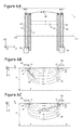
- Fig. 6A illustrates an embodiment of the prior art photonic mixer, that mixes incident amplitude modulated electromagnetic radiation with an electrical signal applied to the substrate 1 ⁇ typically an epi-layer thereof - through source 90.
- Fig 6B shows a cross-section through line lll-lll' of the device illustrated in Fig. 6A .
- the electrical signal applied by source 90 generates a majority current, e.g. majority hole current 99, through the substrate 1.
- the applied electrical signal is typically modulated with the same frequency as the electromagnetic radiation, typically light.
- Electromagnetic masking such as metal regions 60 can be used to prevent that the impinging electromagnetic radiation, such as light penetrates in unwanted areas.
- the present invention relates to a photonic mixer provided with a semiconductor substrate having a field area and means for generating a majority carrier current and an associated electric field in the semiconductor substrate that is doped with a first conductivity type, such that when electromagnetic radiation impinges on the substrate within said field area, pairs of majority and minority carriers are generated in the substrate, resulting in a photocurrent of the minority carriers, said substrate comprising:
- the provision of these zones leads to an increase in the modulation frequency. It is believed that the provision of the zones results therein that the field extends deeper into the substrate. It is has been found relevant that the detection region forms a pn-junction with the substrate, e.g. that the at least one field shaping zone is not present below the detector region. Such undesired presence would hamper the diffusion of minority charge carriers, typically electrons, to the detector region.
- the limiting of the depleted substrate zone laterally may occur in that the field shaping zone delimits the depleted substrate zone.
- the limiting may occur electrically, i.e. in that the field extending through the field shaping zone limits the extension of the depleted substrate zone.
- the limiting may occur geometrically, i.e. in that the junction has a planar or parabolic or similar shape and the depleted substrate zone conforms thereto. Clearly, a combination of these limiting effects may occur as well. A design such that the junction has a parabolic shape, in a cross-sectional view, is deemed to be highly beneficial.
- the detector region comprises detector contact region and a detector collector region sharing a mutual interface, which detector collector region is doped at a lower concentration than the detector contact region and is delimited by the junction with the substrate.
- the provision of a detector collector region results in that the junction has a larger interfacial area and that the junction is present at a deeper level in the substrate. Both effects support an effective collection of the photocurrent.
- the depth at which the junction is present may be smaller, equal to, or larger than the depth to which the field shaping zone extends.
- the junction is present at approximately the same depth as that to which the field shaping regions extend.
- the detector zone may form a pn-junction with the at least one field shaping zones around it. However, this is not necessary and lightly doped substrate (typically p--) could be present between the detector zone (typically n-) and the at least one field shaping zone (typically p-).
- the field area is laterally delimited by at least one contact.
- This contact is preferably a contact region defined in the semiconductor substrate and doped with a dopant of the first conductivity type. More suitably, the dopant concentration is identical to that of the injecting contact region.
- this contact region may have an interface with an additional field shaping zone. This field shaping region preferably laterally delimits the field area.
- the at least one contact may have a ring-shape, but alternatively, could be U-shaped, L-shaped and could further be composed of more than one contact, such as a first and a second U shaped contact, or a first and a second rectangular contact.
- any field shaping region preferably would be ring-shaped
- the contact may be a metal contact on top the semiconductor substrate or a contact within a trench in the semiconductor substrate.
- the semiconductor substrate comprises an active layer with a first side and an opposed second side, wherein said detector region and said injecting correct region are located at the first side and a contact for collecting the majority carrier current is located at the opposed second side of the active layer.
- this embodiment has a field that is primarily vertically oriented, e.g. perpendicular to the first side of the active layer.
- the embodiments will hereinafter also be referred to as those with a lateral contact and with a vertical contact.
- a further option is that there is both a lateral contact and a vertical contact are present.
- the vertical contact is present at the second side of the active layer.
- the contact may be a metal contact on the second side of the semiconductor substrate, in which case the active layer constitutes the body of the substrate.
- the metal contact may cover the complete second side, but that is not deemed necessary.
- the metal contact could also be present in a cavity etched in the semiconductor substrate from the second side.
- the vertical contact may alternatively be a buried region of the first conductivity type. This region may be coupled with a plug or other vertical connection to the first side of the active layer, e.g. the main surface of the semiconductor substrate.
- the vertical contact may in again another version be a top interface of a conductive (e.g. doped) substrate layer, for instance a p+ substrate. More specific implementations hereof will be apparent to the skilled person in the art.
- the advantage of the vertical contact is a higher resolution, which may be easily a factor of 10.
- the higher resolution may be used to provide more individual mixers per unit surface area, or to reduce the size of the photonic mixer.
- the photonic mixer is a differential photonic mixer.
- at least two couples of a current injecting contact region and at least one detector region are present within said field area.
- the advantage of a differential photonic mixer over a photonic mixer with merely one couple, i.e. a single ended photonic mixer is the reduction of measurement time.
- three or more of such couples may be present within the field area.
- a third couple allows further tuning of the frequency range.
- the presence of four couples is advantageous in order to reduce measurement time.
- localizing an object in three dimensions can be carried out within a single measurement. With two couples, localizing an object in three dimensions requires two measurements.
- the four couples are preferably activated in pairs, i.e. as a differential photonic mixer. Individual actuation is however not excluded.
- the photonic mixer can have an optically transparent electrode on the field area for inducing a charge distribution in the field area so as to limit surface recombination.
- the optically transparent electrode can comprise a polysilicon layer
- either a vertical contact or a lateral contact or both are present.
- This embodiment allows to generate a field with both a DC and an AC component.
- the AC component is generated in that the majority carrier current is alternatingly injected from the contact regions of the couples.
- these contact regions are provided at a different voltage, particularly an opposite voltage around a reference level.
- the reference level is typically ground (OV), but that it may have another value.
- the device with a first and a second couple and a contact ⁇ either a lateral contact or a vertical contact ⁇ is found to be very advantageous. It has been found that the demodulation efficiency has increased with 10-20%. This demodulation efficiency defines the efficiency at which charges are separated in the photonic mixer and is hence a measure for the influence of the electric field on the charge carriers forming the photocurrent. This increase is substantial, as it gives rise to threefold improvements in the speed of the measurement system. In addition of being simply better, it is an additional advantage that the number of light emitters in the system may be reduced. Particularly, with a twofold increase in speed, the number of light emitters can be reduced fourfold.
- the contact region laterally limiting is put at a voltage that does not oscillate, but has a constant value during the photonic mixing operation. It thus provides the DC component.
- the voltage of this laterally limiting contact region is preferably such that the photocurrent is directed to the center of the field.
- the laterally limiting contact region is not a current injecting contact region, when used for providing a counterelectrode at a specified DC voltage level.
- a field shaping region may be present below this contact region, but that is not deemed necessary.
- the vertical contact or the lateral contact is preferably operated as a shutter. Thereto, the voltage on the contacts is varied to shut down the DC component of the field, and therewith to ensure that minority carriers will not be attracted by the contact regions.
- the shutter function on the lateral contact or the vertical contact it may be further implemented through the injecting contact region of the couple, particularly in case that more than one couple is present.
- each of said couples has a substantially rectangular shape, when seen in top view, with an edge, a length and a width defining a length/width ratio between 0.05 and 20, said edge being formed by the at least one field shaping zone.
- the design is such that wherein the rectangular shaped couple is provided with a centre, at which a contact region with an underlying field shaping region is present, one ring-shaped or a plurality of detector regions being present on opposed sides of said contact region within said edge.
- the term 'substantially rectangular' includes the specific implementation of a rectangular shape with trimmed corners.
- the injecting current region and the detector region have an elongated shape, or have portions with elongated shape. Therewith, the effective area is increased, leading to improved performance.
- the invention provides a photonic mixer provided with a semiconductor substrate having a field area and means for generating a majority carrier current and an associated electric field in the semiconductor substrate that is doped with a first conductivity type, such that when electromagnetic radiation impinges on the substrate within said field area, pairs of majority and minority carriers are generated in the substrate, resulting in a photocurrent of the minority carriers, said substrate comprising a couple of an injecting contact region for injecting the majority carrier current into the semiconductor substrate and a detector region for collecting the photocurrent, which injecting contact region is doped with a dopant of the first conductivity type at a higher dopant concentration than the semiconductor substrate, and which detector region is doped with a dopant of a second conductivity type opposite to the first conductivity type and that has a junction with the semiconductor substrate, a zone of the semiconductor substrate around said junction being a depleted substrate zone, wherein the detector region is ring shaped and extends around the injecting contact region, a field shaping zone of the first conductivity type with
- the invention provides a photonic mixer provided with a semiconductor substrate having a field area and means for generating a majority carrier current and an associated electric field in the semiconductor substrate that is doped with a first conductivity type, such that when electromagnetic radiation impinges on the substrate within said field area, pairs of majority and minority carriers are generated in the substrate, resulting in a photocurrent of the minority carriers, said substrate comprising a couple of an injecting contact region for injecting the majority carrier current into the semiconductor substrate and a detector region for collecting the photocurrent, which injecting contact region is doped with a dopant of the first conductivity type at a higher dopant concentration than the semiconductor substrate, and which detector region is doped with a dopant of a second conductivity type opposite the first conductivity type and has a junction with the semiconductor substrate, a zone of the semiconductor substrate around said junction being a depleted substrate zone, wherein the semiconductor substrate comprises an active layer with a first side and an opposed second side, wherein said detector region and said injecting correct region are located at the
- the invention relates to a system for measurement of distances between a first and a second object, in particular for a time of flight (TOF) application.
- This system comprises at least one emitter emitting modulated electromagnetic radiation at a first modulation frequency. It further comprises a photonic mixer for detecting said emitted and optionally reflected modulated electromagnetic radiation and in situ mixing a resulting photocurrent with an applied oscillating signal, which oscillates at the modulation frequency, said photonic mixer providing an output signal representative of a phase of the detected radiation.
- the photonic mixer according to the invention is present.
- the invention relates to a method of using a photonic mixer of any of the above aspects of the invention, for time-of-flight range finding applications.
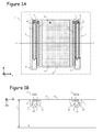
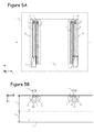
- Fig. 1A is a diagrammatical top view of a first embodiment of the invention
- Fig. 1B is a diagrammatical cross-sectional view of the first embodiment as shown in Fig. 1A , taken along the line D in Fig. 1A
- the photonic mixer comprises a semiconductor substrate 1.
- the semiconductor substrate 1 comprises for instance a bulk silicon substrate that is p-type -doped. It may comprise alternatively another carrier, including glass, sapphire.
- the substrate may further be a SOl-type substrate with a buried insulating layer.
- the shown portion of the semiconductor substrate 1 is in this example a lowly doped epitaxially grown silicon layer (epi-layer) such as typically applied for the definition of semiconductor devices.
- epi-layer epitaxially grown silicon layer
- the epi-layer is p -- -doped, as known per se to the skilled person. It suitably has a thickness between 10 and 50 microns.
- the semiconductor substrate 1 may contain another material than Si, such as SiGe, SiC, GaN, GaAs, InP.
- Contact regions 3, 4 and detector regions 7,8 are formed by implantation of dopant atoms into the substrate, in a manner known per se.
- the contact regions 3,4 are p + or p ++ doped.
- the detector regions 7,8 comprise, in this example, detector contact regions (n + ) and detector collector regions (n - ), which share a mutual interface.
- the detector regions 7,8 are doped with a dopant of the second conductivity type opposite to the first conductivity type, e.g. n-type doped.
- the dopant concentration of the detector contact regions (n + ) is higher than that of the detector collector regions (n - ).
- the detector regions 7,8 ⁇ in this example the detector collector regions thereof - have an interface with the substrate 1, which is a junction, i.e. a pn-junction. In operation, the pn-junction is typically reversed biased. Depleted substrate zones 101, 102 are present around said junction 11, 12 in the substrate 1.
- field shaping zones 13, 14 are present.
- the field shaping zones 13, 14 are of the first conductivity type (p-type). They extend substantially perpendicularly into the semiconductor substrate 1.
- the field shaping zones 13, 14 have a dopant concentration (p - ) higher than the dopant concentration of the substrate 1 (p -- ), for example between the dopant concentrations of the substrate 1 (p -- ) and the injecting contact regions 3,4 (p + ).
- the at least one detector region 7,8 is located, when viewed in a top view, between a first and a second field shaping zones 13, 14, so as to limit laterally said depleted substrate zone 101, 102.
- the field shaping regions 13, 14 extend into the substrate 1 to a depth of for instance 0.5-5 microns, preferably 1-2 microns.
- the field shaping zones 13, 14 of the first conductivity type define a lateral edge 113 of a couple of an injecting contact region 3,4 and a detection region 7,8.
- the depleted substrate zones 101, 102 would extend much more widely, particularly as a sphere extending up to the substrate surface. It would moreover have an asymmetrical shape; the presence of the contact region 3,4 would set a limit on one side, but not on the other.
- the junction 11, 12 has in cross-sectional view as shown in Fig. 1B , a parabolic shape.
- the depleted regions 101, 102 are effectively shells around this junctions 11, 12. Hence they extend more perpendicularly to the substrate surface (also referred to as vertical) than lateral. This is also the case, when the detector region 7,8 extends deeper into the substrate 1 than the field shaping regions 13, 14.
- the shape of the junction is not parabolic or something similar to that.
- the field shaping regions 13, 14 laterally limit the depleted regions directly in this case, e.g. to the substrate area between them.
- an optically transparent electrode 50 is present on a surface of the substrate 1. It is separated from the substrate surface by an insulating layer 52, such as an oxide. However, high-K dielectrics such as tantalumoxide and other materials could be used alternatively.
- the optically transparent electrode 50 is suitably a layer of polysilicon. This may be doped in order to increase the conductivity with a suitable dopant.
- the electrode 50 may be applied to reduce surface recombination by applying a repulsive force on the electrons. Suitably, in operation, a voltage is applied on this electrode 50 in order to enhance the repulsive force. Thereto, a terminal 51 is present.
- the electrode 50 is patterned so as not to overlie the detector regions 7,8, the contact regions 3,4 and the field shaping zones 13, 14. It does not need to cover the complete field area 2.
- the top view of Fig. 1A shows the layout of this first embodiment.
- the field shaping zones 13, 14 are at opposite edges of the field area 2, at which electromagnetic radiation will impinge the substrate so as to be converted into minority and majority carriers.
- the detector regions 7,8 and the contact regions 3,4 are elongate regions extending parallel to each other and are provided with terminals 9,10 and 5,6 respectively. These terminals 9,10, 5,6 are in this example limited to areas at an end of the regions 7,8, 3,4 but they not need to be located exactly there. There can be multiple terminals on the same contact region.
- Masks 21 overlie the detector regions 7,8 in order to shield those from incoming electromagnetic radiation.
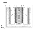
- Fig. 2 is a diagrammatical top view of a second embodiment of the invention.
- this embodiment comprises four contact regions 3,4,15,16 and merely two detector regions 7,8.
- the additional contact regions 15,16 are located at extreme edges of the field area 2.
- Field shaping zones 19, 20 are defined below the additional contact regions 15, 16 and terminals 17, 18 are defined thereon.
- the additional contact regions 15,16 are designed to be put on a constant voltage during the photonic mixing operation.
- the contact regions 3,4 are intended to be put on alternating voltages. Therewith, one may apply a field with both a AC component and a DC component. The application of such field is found to limit crosstalk.
- This option is not limited to the presently shown layout, but is effectively an option for any of the embodiments having a first and a second couple of both detector region and contact region in combination with laterally remote contact regions acting as a DC counterelectrode.
- leaving out one detector region may have a substantially negative impact on the overall collected photocurrent, and hence the efficiency of the photonic mixer.
- the detector is elongate, and the impact is expected to be small.
- Another consequence of removal of the second detector region is that the number of measurements to be carried out sequentially may increase. Measurement of at least three different phases is required in order to obtain a distance measurement of an object in a time of flight method. With one detector region, there is merely one output, and thus three sequential measurements are needed. With two detector regions, two sequential measurements are sufficient. With four detector regions, one sequential measurement appears sufficient .
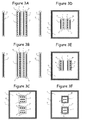
- Fig. 3A-3F and Fig. 4A-4F show in total twelve designs for use in the invention, in simplified diagrammatical topviews.
- Fig. 3B shows a simplified diagrammatical topview representation of the photonic mixer represented in Fig 2 , whereby only the necessary subset of elements is represented.
- the thick solid lines represent the contact regions of the first conductivity type, p + -regions 3,4, 15,16 for applying the majority current.
- the thick dashed line represents the detection regions 7,8.
- the dotted line represents the junction interface 11, 12 of the detector collector regions with the surrounding regions.
- the dashed lines around the thick solid lines represent the outside of the field shaping zones 13, 14, 19, 20.
- Fig. 3A is a design largely corresponding to the design of Fig. 3B . The difference relates to the positioning of the detector region and contact regions within the field shaping zones.
- the detector regions 7,8 are defined between the contact regions 3,4 and the additional contact regions 15, 16 at the edges of the field area 2.
- the contact regions 3,4 are defined between the detector regions 7,8 and the additional contact regions 15, 16 at the edges of the field area 2.
- the set up of Fig. 3A tends to enhance the speed of the diffusion process in which the minority charge carriers diffuse to the detector regions 7,8 to make up the photocurrent.
- Fig. 3C-3F and Fig.4A-4F show designs comprising a ring-shaped additional contact region 30 at the edge of the field area 2.
- the advantage of the designs here is that the field is oriented to the center instead of between a first and a second elongated and parallel contact regions. Such center-oriented field is deemed to be beneficial for further increasing the modulation frequency.
- the additional contact region 30 is present within a field shaping zone 31.
- Fig. 4E and 4F are identical to those of Fig. 3E and Fig. 4A respectively, except that the field shaping zone below the ring shaped contact region at the edge of the field area 2 has been left out.
- the contact regions and detector regions are present in couples having a rectangular shape defined by the field shaping zone.
- FIG. 3C A first group of the designs is shown in Fig. 3C , Fig 4A and Fig. 4D .
- These designs comprise couples of at least one contact region 3, 4 and two detector regions 32, 33 and 36, 37.
- the edge of the couple is defined by the field shaping zone 13, 14.
- Windows 34, 35 and 38, 39 are present within the single field shaping zone 13, 14 around the detector regions 32,33 and 36,37.
- a contact region 3, 4 is present between a first and a second detector region.
- the contact region 3,4 and detector regions 32, 33, 36, 37 are all of elongated shape, or comprise elongated portions.
- the orientation of the couples is identical, and more specifically such that a detector regions 32, 33, 36, 37 in the two couples are oriented in parallel and in a single row, with their long sides towards each other. This is however not deemed necessary.
- the orientation of all of them may be such that the detector regions 32, 33, 36, 37 in the two couples are present in two rows of two, with their short sides towards each other. The one couple may be shifted towards the other.
- the two couples may also be located on a diagonal.
- the orientation of the two couples may include an angle of anything between ⁇ 90 and +90 degrees.
- the design is such that the contact regions 3, 4 in the couples are oriented in parallel to a portion of the ring-shaped contact region 30 at the edge of the field area 2. It is moreover preferred that the couples are present with their centres on a middle line or a diagonal line of the field area 2.
- Such orientation leads to most regular, preferably symmetric set up of the electric field, and hence with a field that is least disturbed.
- Fig. 4A comprises two additional contact regions 40, 41 and 42, 43 per couple.
- the additional contact regions 40-43 are defined between the detector regions 32, 33, 36, 37 and the edge of the couple 13, 14. While the shown U-shape is preferred, a rectangular shape or an L-shape is not excluded.
- the design of Fig 4D has even more contact regions. In this design, the three contact regions per couple 3,41,42 and 4,43,44 shown in Fig.4A are merged into a 8-shaped contact region 3,4. This is beneficial for the distribution of the field.
- FIG. 3F shows a design wherein the detector 7,8 is present at the heart of the couple.
- a ring-shaped contact region 3,4 circumvents the detector 7,8.
- Fig.4B shows a design with an inner contact region 3,4 within a first field shaping zone 13, 14, a ring shaped detector region 7,8 and ring shaped contact region 44, 45 within a second field shaping zone 23, 24.
- Fig. 4C shows a similar design, in which the outer ring-shaped contact region is absent, leaving the second field shaping region 23, 24 floating.
- the advantage of this type of designs is that the radial symmetry extends into each couple.
- the field shaping zones 13,14 extend deeper into the semiconductor substrate than the laterally limiting field shaping regions 23,24. This can be achieved, for example, by using an implantation type known to the skilled person as a Deep Pwell for field shaping zones 13,14. This deeper extension of the inner field shaping zones further improves the distribution of the electric field. Additionally, the deeper extension improves the quality of the contact region 3,4 with the substrate 1. Particularly, said quality is improved by preventing or at least reducing any negative impact resulting from a depletion of the typically n-type detector region 7,8.
- the deeper extension is specifically advantageous for this second subset of designs, and most suitable in combination with a design in which the second field shaping region 23, 24 is left floating.
- the use of an implantation extending deeper into the substrate may also be applied to any of the other subsets.
- the deeper implantation could be present below contact region 4, e.g. In that case, there is a gradual transition from the deep well to the rest of the field shaping zone.
- the deep well is herein preferably applied locally at a centre of the couple.
- FIG. 3D and 3E A third subset of designs is constituted by Fig. 3D and 3E .
- the elongate couples also shown in Fig. 3A and 3B are located within the field area limited by a ring-shaped contact region.
- Fig. 7 is a graph showing the relationship between the modulation contrast C and the modulation frequency f for a prior art photonic mixer and an embodiment of the photonic mixer according to the invention.
- the photonic mixer used to generate the experimental data had the design as shown in Fig. 4A .
- the modulation contrast or modulation efficiency defines the efficiency at which charges are separated in the photonic mixer and is hence a measure for the influence of the electric field on the charge carriers forming the photocurrent.
- the modulation contrast for the prior art photonic mixer reduces substantially already below 1 MHz. At 1 MHz it is approximately 85%. At 10 MHz, it has reduced to approximately 40%. At 100MHz, the contrast is less than 20%. Such low contrast leads a considerable disadvantage.
- the modulation contrast for the photonic mixer according to the invention reduces slowly. At 5 MHz, it is still 80%. Around 50 MHz, the contrast is 60%, and at 100 MHz, the contrast is still 50%. These are contrasts that are sufficiently good to do an appropriate distance measurement.
- the increase in contrast at higher modulation frequencies leads to substantial increases in the speed of the measurement system. In addition of being simply better, it is an additional advantage that the number of light emitters in the system may be reduced. Particularly, with a twofold increase in speed, the number of light emitters can be reduced fourfold.
- Fig. 5A is a diagrammatical top view of a third embodiment of the invention
- Fig. 5B is a diagrammatical cross-sectional view of the third embodiment as shown in Fig. 5A , taken along the line D in Fig. 5A.
- Fig. 5 shows a substrate with an active layer 1 with p -- doping and a bottom substrate layer 80 with in this example p-doping.
- the bottom substrate layer 80 may have a higher doping, such as p + to be electrically conductive.
- Such substrates are commercially available and known to the skilled person. The exact doping level is a matter of implementation.
- the bottom substrate layer 80 is a typical monocrystalline p-doped silicon substrate and the active layer 1 is an epi-layer.
- the bottom contact is effectively constituted by the bottom substrate layer 80 plus a metal contact 81 thereon. It is thus a vertical contact, as discussed in the introduction.
- the field will be extending between the injecting contact regions 3,4 and ultimately the metal contact 81.
- the field effectively extends between the injecting contact regions 3,4 and the top of the bottom substrate layer 80.
- current is injected through the contact regions 3,4 into the active layer 1 at a modulation frequency, alternating between the first contact region 3 and the second region 4.
- read out circuits and control circuits are suitably monolithically integrated, i.e. transistors and/or other semiconductor components are defined in the (active layer) of the semiconductor substrate, and interconnect structure is provided to define the desired circuit topology.
- Control of the photonic mixer not merely relates to the provision of the voltages to the contact regions, but also includes the provision of signals so as to reset the photonic mixer, particularly before a subsequent measurement. Such signal provision is typically achieved with a shutter function, as explained above.
- the electromagnetic radiation may be provided to the front side of the substrate, but alternatively also to the backside of the substrate, particularly in combination with reduction of substrate thickness and optionally application of a carrier to the front side.
- More than two couples may be present within the field area.
- Terms vertical, above and below are defined with reference to the orientation of a semiconductor substrate during processing, in which the front side is at the top (above) and the substrate surface defines the laterally extending direction. The vertical is then the normal to this substrate surface. Subdivision of one elongate contact region, detector region and also of the field shaping zones into several smaller regions/zones is not excluded
- the invention may be alternatively characterized in the following way: a photonic mixer provided with a semiconductor substrate having a field area and means for generating a majority carrier current and an associated electric field in the semiconductor substrate that is doped with a first conductivity type, such that when electromagnetic radiation impinges on the substrate within said field area, pairs of majority and minority carriers are generated in the substrate, resulting in a photocurrent of the minority carriers, said substrate comprising:
Applications Claiming Priority (3)
| Application Number | Priority Date | Filing Date | Title |
|---|---|---|---|
| GB0918040A GB2474631A (en) | 2009-10-14 | 2009-10-14 | Photonic Mixer |
| GB0920866A GB0920866D0 (en) | 2009-11-27 | 2009-11-27 | Photonic mixer and use thereof |
| GB0922319A GB0922319D0 (en) | 2009-12-21 | 2009-12-21 | Photonic mixer and use thereof |
Publications (3)
| Publication Number | Publication Date |
|---|---|
| EP2330637A2 true EP2330637A2 (de) | 2011-06-08 |
| EP2330637A3 EP2330637A3 (de) | 2014-07-23 |
| EP2330637B1 EP2330637B1 (de) | 2019-07-24 |
Family
ID=43910547
Family Applications (1)
| Application Number | Title | Priority Date | Filing Date |
|---|---|---|---|
| EP10187389.1A Active EP2330637B1 (de) | 2009-10-14 | 2010-10-13 | Photonischer mischer, dessen verwendung und system das den photonischen mischer beinhaltet |
Country Status (9)
| Country | Link |
|---|---|
| US (1) | US8294882B2 (de) |
| EP (1) | EP2330637B1 (de) |
| JP (1) | JP5593487B2 (de) |
| KR (1) | KR101747420B1 (de) |
| CN (1) | CN102044547B (de) |
| CA (1) | CA2760709A1 (de) |
| GB (1) | GB2474631A (de) |
| IL (1) | IL208698A (de) |
| TW (1) | TWI545792B (de) |
Cited By (34)
| Publication number | Priority date | Publication date | Assignee | Title |
|---|---|---|---|---|
| WO2013104718A3 (en) * | 2012-01-10 | 2013-09-06 | Softkinetic Sensors Nv | Multispectral sensor |
| WO2015197685A1 (en) * | 2014-06-27 | 2015-12-30 | Softkinetic Sensors Nv | Majority current assisted radiation detector device |
| WO2017079536A1 (en) * | 2015-11-06 | 2017-05-11 | Artilux Corporation | High-speed light sensing apparatus |
| US9786715B2 (en) | 2015-07-23 | 2017-10-10 | Artilux Corporation | High efficiency wide spectrum sensor |
| US9893112B2 (en) | 2015-08-27 | 2018-02-13 | Artilux Corporation | Wide spectrum optical sensor |
| US9954016B2 (en) | 2015-08-04 | 2018-04-24 | Artilux Corporation | Germanium-silicon light sensing apparatus |
| WO2018160721A1 (en) * | 2017-02-28 | 2018-09-07 | Artilux Corporation | High-speed light sensing apparatus ii |
| WO2018206606A1 (en) * | 2017-05-08 | 2018-11-15 | Vrije Universiteit Brussel | Detector for fast-gated detection of electromagnetic radiation |
| EP3518418A1 (de) * | 2018-01-30 | 2019-07-31 | Vrije Universiteit Brussel | Elektronischer mischer |
| US10418407B2 (en) | 2015-11-06 | 2019-09-17 | Artilux, Inc. | High-speed light sensing apparatus III |
| US10564718B2 (en) | 2015-08-04 | 2020-02-18 | Artilux, Inc. | Eye gesture tracking |
| EP3525449A4 (de) * | 2017-08-30 | 2020-05-27 | Sony Semiconductor Solutions Corporation | Bilderfassungselement und bilderfassungsvorrichtung |
| US10707260B2 (en) | 2015-08-04 | 2020-07-07 | Artilux, Inc. | Circuit for operating a multi-gate VIS/IR photodiode |
| US10739443B2 (en) | 2015-11-06 | 2020-08-11 | Artilux, Inc. | High-speed light sensing apparatus II |
| US10741598B2 (en) | 2015-11-06 | 2020-08-11 | Atrilux, Inc. | High-speed light sensing apparatus II |
| CN111638402A (zh) * | 2020-05-21 | 2020-09-08 | 山西大学 | 测量微波电场中微波信号的频率的方法及系统 |
| US10777692B2 (en) | 2018-02-23 | 2020-09-15 | Artilux, Inc. | Photo-detecting apparatus and photo-detecting method thereof |
| EP3640989A4 (de) * | 2018-07-18 | 2020-10-21 | Sony Semiconductor Solutions Corporation | Lichtempfangselement und entfernungsmessmodul |
| CN111965661A (zh) * | 2020-08-10 | 2020-11-20 | 苏州离娄科技有限公司 | 双栅结构间接飞行时间器件、主动光电探测组件和光电系统 |
| US10854770B2 (en) | 2018-05-07 | 2020-12-01 | Artilux, Inc. | Avalanche photo-transistor |
| US10861888B2 (en) | 2015-08-04 | 2020-12-08 | Artilux, Inc. | Silicon germanium imager with photodiode in trench |
| US10886311B2 (en) | 2018-04-08 | 2021-01-05 | Artilux, Inc. | Photo-detecting apparatus |
| US10886312B2 (en) | 2015-11-06 | 2021-01-05 | Artilux, Inc. | High-speed light sensing apparatus II |
| US10969877B2 (en) | 2018-05-08 | 2021-04-06 | Artilux, Inc. | Display apparatus |
| US11081509B2 (en) | 2017-05-08 | 2021-08-03 | Vrije Universiteit Brussel | Detector for fast-gated detection of electromagnetic radiation |
| US11102433B2 (en) | 2017-08-09 | 2021-08-24 | Sony Semiconductor Solutions Corporation | Solid-state imaging device having a photoelectric conversion element with multiple electrodes |
| US11105928B2 (en) | 2018-02-23 | 2021-08-31 | Artilux, Inc. | Light-sensing apparatus and light-sensing method thereof |
| EP3907526A1 (de) * | 2020-05-08 | 2021-11-10 | Melexis Technologies NV | Photonische mischvorrichtung |
| US11398519B2 (en) | 2017-12-09 | 2022-07-26 | National University Corporation Shizuoka University | Charge modulation element and solid-state imaging device |
| WO2022194571A1 (en) * | 2021-03-17 | 2022-09-22 | Sony Semiconductor Solutions Corporation | A pixel unit, a pixel array, a time-of-flight imaging sensor and an electronic device |
| US11482553B2 (en) | 2018-02-23 | 2022-10-25 | Artilux, Inc. | Photo-detecting apparatus with subpixels |
| US11480658B2 (en) | 2016-03-04 | 2022-10-25 | Sony Corporation | Imaging apparatus and distance measurement system |
| US11574942B2 (en) | 2018-12-12 | 2023-02-07 | Artilux, Inc. | Semiconductor device with low dark noise |
| US11652184B2 (en) | 2019-08-28 | 2023-05-16 | Artilux, Inc. | Photo-detecting apparatus with low dark current |
Families Citing this family (30)
| Publication number | Priority date | Publication date | Assignee | Title |
|---|---|---|---|---|
| US9190540B2 (en) * | 2011-12-21 | 2015-11-17 | Infineon Technologies Ag | Photo cell devices for phase-sensitive detection of light signals |
| JP5977366B2 (ja) * | 2013-01-10 | 2016-08-24 | ソフトキネティック センサー エヌブイ | カラー不可視光センサ、例えば、irセンサ、すなわち、マルチスペクトルセンサ |
| EP3193190B1 (de) * | 2016-01-15 | 2023-04-12 | Sony Depthsensing Solutions N.V. | Detektorvorrichtung mit majoritätsstrom und schaltung zur steuerung des stroms |
| US10191154B2 (en) | 2016-02-11 | 2019-01-29 | Massachusetts Institute Of Technology | Methods and apparatus for time-of-flight imaging |
| TWI806127B (zh) * | 2016-02-12 | 2023-06-21 | 光程研創股份有限公司 | 光學裝置及光學系統 |
| US10337993B2 (en) | 2016-04-15 | 2019-07-02 | Massachusetts Institute Of Technology | Methods and apparatus for fluorescence lifetime imaging with periodically modulated light |
| KR102632100B1 (ko) * | 2016-09-09 | 2024-02-01 | 주식회사 디비하이텍 | 광 검출 장치 |
| JP6691101B2 (ja) | 2017-01-19 | 2020-04-28 | ソニーセミコンダクタソリューションズ株式会社 | 受光素子 |
| WO2018135320A1 (ja) * | 2017-01-19 | 2018-07-26 | ソニーセミコンダクタソリューションズ株式会社 | 受光素子、撮像素子、および、撮像装置 |
| EP3602109B1 (de) * | 2017-03-19 | 2021-01-20 | Kovilta Oy | Systeme und verfahren zur modulierten bildaufnahme |
| KR20200062075A (ko) | 2017-09-28 | 2020-06-03 | 소니 세미컨덕터 솔루션즈 가부시키가이샤 | 촬상 소자 및 촬상 장치 |
| DE102019101752B4 (de) * | 2018-02-05 | 2020-08-06 | pmdtechnologies ag | Pixelarray für eine Kamera, Kamera und Lichtlaufzeitkamerasystem mit einer derartigen Kamera |
| JP7054639B2 (ja) * | 2018-03-16 | 2022-04-14 | ソニーセミコンダクタソリューションズ株式会社 | 受光素子および電子機器 |
| CN110739321A (zh) | 2018-07-18 | 2020-01-31 | 索尼半导体解决方案公司 | 受光元件以及测距模块 |
| TW202006788A (zh) * | 2018-07-18 | 2020-02-01 | 日商索尼半導體解決方案公司 | 受光元件及測距模組 |
| CN210325800U (zh) | 2018-07-18 | 2020-04-14 | 索尼半导体解决方案公司 | 受光元件以及测距模块 |
| JP7175655B2 (ja) | 2018-07-18 | 2022-11-21 | ソニーセミコンダクタソリューションズ株式会社 | 受光素子および測距モジュール |
| CN110739322A (zh) | 2018-07-18 | 2020-01-31 | 索尼半导体解决方案公司 | 受光元件以及测距模块 |
| JP7362198B2 (ja) | 2018-07-18 | 2023-10-17 | ソニーセミコンダクタソリューションズ株式会社 | 受光素子、測距モジュール、および、電子機器 |
| CN110739324A (zh) | 2018-07-18 | 2020-01-31 | 索尼半导体解决方案公司 | 受光元件以及测距模块 |
| KR102613095B1 (ko) | 2018-07-18 | 2023-12-14 | 소니 세미컨덕터 솔루션즈 가부시키가이샤 | 수광 소자 및 거리 측정 모듈 |
| JP2020013906A (ja) | 2018-07-18 | 2020-01-23 | ソニーセミコンダクタソリューションズ株式会社 | 受光素子および測距モジュール |
| JP2020088142A (ja) | 2018-11-26 | 2020-06-04 | ソニーセミコンダクタソリューションズ株式会社 | 受光素子および電子機器 |
| TW202032773A (zh) | 2019-02-01 | 2020-09-01 | 日商索尼半導體解決方案公司 | 受光元件、固體攝像裝置及測距裝置 |
| KR20210002880A (ko) * | 2019-07-01 | 2021-01-11 | 에스케이하이닉스 주식회사 | 픽셀 및 이를 포함하는 이미지 센서 |
| TW202114241A (zh) | 2019-09-25 | 2021-04-01 | 日商索尼半導體解決方案公司 | 光接收元件、距離測量模組及電子儀器 |
| US20220406827A1 (en) | 2019-10-30 | 2022-12-22 | Sony Semiconductor Solutions Corporation | Light receiving element, distance measurement module, and electronic equipment |
| CN114365287A (zh) | 2019-10-30 | 2022-04-15 | 索尼半导体解决方案公司 | 受光元件、测距模块和电子设备 |
| TW202133460A (zh) | 2020-01-20 | 2021-09-01 | 日商索尼半導體解決方案公司 | 受光元件、攝像元件及攝像裝置 |
| WO2022200055A1 (en) * | 2021-03-25 | 2022-09-29 | Sony Semiconductor Solutions Corporation | Time-of-flight demodulation circuitry and a time-of-flight demodulation method |
Citations (3)
| Publication number | Priority date | Publication date | Assignee | Title |
|---|---|---|---|---|
| WO1998010255A1 (de) | 1996-09-05 | 1998-03-12 | Rudolf Schwarte | Verfahren und vorrichtung zur bestimmung der phasen- und/oder amplitudeninformation einer elektromagnetischen welle |
| WO1999060629A1 (de) | 1998-05-18 | 1999-11-25 | Rudolf Schwarte | Vorrichtung und verfahren zur erfassung von phase und amplitude elektromagnetischer wellen |
| EP1513202A1 (de) | 2003-09-02 | 2005-03-09 | Vrije Universiteit Brussel | Ein durch einen Strom aus Majoritätsträgern unterstützter Detektor für elektromagnetische Strahlung |
Family Cites Families (8)
| Publication number | Priority date | Publication date | Assignee | Title |
|---|---|---|---|---|
| EP0883187A1 (de) * | 1997-06-04 | 1998-12-09 | Interuniversitair Micro-Elektronica Centrum Vzw | Detektor für elektromagnetische Strahlung, Pixelstruktur mit höher Empfindlichkeit mit Verwendung dieses Detektors und Verfahren zu dessen Herstellung |
| EP0875939A1 (de) * | 1997-04-30 | 1998-11-04 | Interuniversitair Micro-Elektronica Centrum Vzw | Räumlich modulierter Detektor für elektromagnetische Strahlung |
| JP4241527B2 (ja) * | 1999-02-25 | 2009-03-18 | キヤノン株式会社 | 光電変換素子 |
| JP2002083993A (ja) * | 2000-09-06 | 2002-03-22 | Toshiba Corp | 光半導体受光素子およびその製造方法 |
| JP2004512723A (ja) * | 2000-10-16 | 2004-04-22 | シュワルテ ルドルフ | 信号波を検出して処理する方法およびデバイス |
| CN100580940C (zh) * | 2003-09-18 | 2010-01-13 | Ic-豪斯有限公司 | 光电传感器和用于三维距离测量的装置 |
| JP4971891B2 (ja) * | 2007-07-03 | 2012-07-11 | 浜松ホトニクス株式会社 | 裏面入射型測距センサ及び測距装置 |
| EP2081004A1 (de) * | 2008-01-17 | 2009-07-22 | Vrije Universiteit Brussel | Lichtspektrometer |
-
2009
- 2009-10-14 GB GB0918040A patent/GB2474631A/en not_active Withdrawn
-
2010
- 2010-02-26 CN CN201010134987.8A patent/CN102044547B/zh active Active
- 2010-03-25 JP JP2010069876A patent/JP5593487B2/ja active Active
- 2010-10-13 TW TW099134825A patent/TWI545792B/zh active
- 2010-10-13 KR KR1020100099815A patent/KR101747420B1/ko active IP Right Grant
- 2010-10-13 EP EP10187389.1A patent/EP2330637B1/de active Active
- 2010-10-14 IL IL208698A patent/IL208698A/en active IP Right Grant
- 2010-10-14 US US12/904,204 patent/US8294882B2/en active Active
-
2011
- 2011-12-06 CA CA2760709A patent/CA2760709A1/en not_active Abandoned
Patent Citations (3)
| Publication number | Priority date | Publication date | Assignee | Title |
|---|---|---|---|---|
| WO1998010255A1 (de) | 1996-09-05 | 1998-03-12 | Rudolf Schwarte | Verfahren und vorrichtung zur bestimmung der phasen- und/oder amplitudeninformation einer elektromagnetischen welle |
| WO1999060629A1 (de) | 1998-05-18 | 1999-11-25 | Rudolf Schwarte | Vorrichtung und verfahren zur erfassung von phase und amplitude elektromagnetischer wellen |
| EP1513202A1 (de) | 2003-09-02 | 2005-03-09 | Vrije Universiteit Brussel | Ein durch einen Strom aus Majoritätsträgern unterstützter Detektor für elektromagnetische Strahlung |
Cited By (71)
| Publication number | Priority date | Publication date | Assignee | Title |
|---|---|---|---|---|
| WO2013104718A3 (en) * | 2012-01-10 | 2013-09-06 | Softkinetic Sensors Nv | Multispectral sensor |
| US10056416B2 (en) | 2014-06-27 | 2018-08-21 | Softkinetic Sensors Nv | Majority current assisted radiation detector device |
| WO2015197685A1 (en) * | 2014-06-27 | 2015-12-30 | Softkinetic Sensors Nv | Majority current assisted radiation detector device |
| EP2960952A1 (de) * | 2014-06-27 | 2015-12-30 | Softkinetic Sensors N.V. | Strahlungsdetektor mit Unterstützung durch einen Stromfluss von Majoritätsladungsträgern |
| KR20170040124A (ko) * | 2014-06-27 | 2017-04-12 | 소프트키네틱 센서스 엔브이 | 다수 전류에 의해 보조되는 방사선 검출기 장치 |
| BE1023562B1 (fr) * | 2014-06-27 | 2017-05-04 | Softkinetic Sensors Nv | Un dispositif detecteur assiste par un courant majoritaire. |
| US10615219B2 (en) | 2015-07-23 | 2020-04-07 | Artilux, Inc. | High efficiency wide spectrum sensor |
| US9786715B2 (en) | 2015-07-23 | 2017-10-10 | Artilux Corporation | High efficiency wide spectrum sensor |
| US10269862B2 (en) | 2015-07-23 | 2019-04-23 | Artilux Corporation | High efficiency wide spectrum sensor |
| US11335725B2 (en) | 2015-07-23 | 2022-05-17 | Artilux, Inc. | High efficiency wide spectrum sensor |
| US11756969B2 (en) | 2015-08-04 | 2023-09-12 | Artilux, Inc. | Germanium-silicon light sensing apparatus |
| US10056415B2 (en) | 2015-08-04 | 2018-08-21 | Artilux Corporation | Germanium-silicon light sensing apparatus |
| US10964742B2 (en) | 2015-08-04 | 2021-03-30 | Artilux, Inc. | Germanium-silicon light sensing apparatus II |
| US10861888B2 (en) | 2015-08-04 | 2020-12-08 | Artilux, Inc. | Silicon germanium imager with photodiode in trench |
| US9954016B2 (en) | 2015-08-04 | 2018-04-24 | Artilux Corporation | Germanium-silicon light sensing apparatus |
| US10256264B2 (en) | 2015-08-04 | 2019-04-09 | Artilux Corporation | Germanium-silicon light sensing apparatus |
| US10761599B2 (en) | 2015-08-04 | 2020-09-01 | Artilux, Inc. | Eye gesture tracking |
| US10269838B2 (en) | 2015-08-04 | 2019-04-23 | Artilux Corporation | Germanium-silicon light sensing apparatus |
| US11755104B2 (en) | 2015-08-04 | 2023-09-12 | Artilux, Inc. | Eye gesture tracking |
| US10756127B2 (en) | 2015-08-04 | 2020-08-25 | Artilux, Inc. | Germanium-silicon light sensing apparatus |
| US10707260B2 (en) | 2015-08-04 | 2020-07-07 | Artilux, Inc. | Circuit for operating a multi-gate VIS/IR photodiode |
| US10685994B2 (en) | 2015-08-04 | 2020-06-16 | Artilux, Inc. | Germanium-silicon light sensing apparatus |
| US10564718B2 (en) | 2015-08-04 | 2020-02-18 | Artilux, Inc. | Eye gesture tracking |
| US10770504B2 (en) | 2015-08-27 | 2020-09-08 | Artilux, Inc. | Wide spectrum optical sensor |
| US10157954B2 (en) | 2015-08-27 | 2018-12-18 | Artilux Corporation | Wide spectrum optical sensor |
| US9893112B2 (en) | 2015-08-27 | 2018-02-13 | Artilux Corporation | Wide spectrum optical sensor |
| US11749696B2 (en) | 2015-11-06 | 2023-09-05 | Artilux, Inc. | High-speed light sensing apparatus II |
| US10418407B2 (en) | 2015-11-06 | 2019-09-17 | Artilux, Inc. | High-speed light sensing apparatus III |
| US11637142B2 (en) | 2015-11-06 | 2023-04-25 | Artilux, Inc. | High-speed light sensing apparatus III |
| US10353056B2 (en) | 2015-11-06 | 2019-07-16 | Artilux Corporation | High-speed light sensing apparatus |
| US11579267B2 (en) | 2015-11-06 | 2023-02-14 | Artilux, Inc. | High-speed light sensing apparatus |
| US10741598B2 (en) | 2015-11-06 | 2020-08-11 | Atrilux, Inc. | High-speed light sensing apparatus II |
| US10310060B2 (en) | 2015-11-06 | 2019-06-04 | Artilux Corporation | High-speed light sensing apparatus |
| US11131757B2 (en) | 2015-11-06 | 2021-09-28 | Artilux, Inc. | High-speed light sensing apparatus |
| US10886309B2 (en) | 2015-11-06 | 2021-01-05 | Artilux, Inc. | High-speed light sensing apparatus II |
| US10254389B2 (en) | 2015-11-06 | 2019-04-09 | Artilux Corporation | High-speed light sensing apparatus |
| WO2017079536A1 (en) * | 2015-11-06 | 2017-05-11 | Artilux Corporation | High-speed light sensing apparatus |
| US10795003B2 (en) | 2015-11-06 | 2020-10-06 | Artilux, Inc. | High-speed light sensing apparatus |
| US11747450B2 (en) | 2015-11-06 | 2023-09-05 | Artilux, Inc. | High-speed light sensing apparatus |
| US10739443B2 (en) | 2015-11-06 | 2020-08-11 | Artilux, Inc. | High-speed light sensing apparatus II |
| US10886312B2 (en) | 2015-11-06 | 2021-01-05 | Artilux, Inc. | High-speed light sensing apparatus II |
| EP3404717A1 (de) * | 2015-11-06 | 2018-11-21 | Artilux Corporation | Hochgeschwindigkeitslichtmessvorrichtung |
| US11480658B2 (en) | 2016-03-04 | 2022-10-25 | Sony Corporation | Imaging apparatus and distance measurement system |
| CN110870070A (zh) * | 2017-02-28 | 2020-03-06 | 奥特逻科公司 | 高速光感测设备ii |
| WO2018160721A1 (en) * | 2017-02-28 | 2018-09-07 | Artilux Corporation | High-speed light sensing apparatus ii |
| WO2018206606A1 (en) * | 2017-05-08 | 2018-11-15 | Vrije Universiteit Brussel | Detector for fast-gated detection of electromagnetic radiation |
| US11081509B2 (en) | 2017-05-08 | 2021-08-03 | Vrije Universiteit Brussel | Detector for fast-gated detection of electromagnetic radiation |
| US11102433B2 (en) | 2017-08-09 | 2021-08-24 | Sony Semiconductor Solutions Corporation | Solid-state imaging device having a photoelectric conversion element with multiple electrodes |
| US11309346B2 (en) | 2017-08-30 | 2022-04-19 | Sony Semiconductor Solutions Corporation | Imaging element and imaging apparatus |
| EP3525449A4 (de) * | 2017-08-30 | 2020-05-27 | Sony Semiconductor Solutions Corporation | Bilderfassungselement und bilderfassungsvorrichtung |
| US11398519B2 (en) | 2017-12-09 | 2022-07-26 | National University Corporation Shizuoka University | Charge modulation element and solid-state imaging device |
| WO2019149788A1 (en) * | 2018-01-30 | 2019-08-08 | Vrije Universiteit Brussel | Electronic mixer |
| US11271526B2 (en) | 2018-01-30 | 2022-03-08 | Vrije Universiteit Brussel | Electronic mixer |
| EP3518418A1 (de) * | 2018-01-30 | 2019-07-31 | Vrije Universiteit Brussel | Elektronischer mischer |
| US11482553B2 (en) | 2018-02-23 | 2022-10-25 | Artilux, Inc. | Photo-detecting apparatus with subpixels |
| US11105928B2 (en) | 2018-02-23 | 2021-08-31 | Artilux, Inc. | Light-sensing apparatus and light-sensing method thereof |
| US11630212B2 (en) | 2018-02-23 | 2023-04-18 | Artilux, Inc. | Light-sensing apparatus and light-sensing method thereof |
| US10777692B2 (en) | 2018-02-23 | 2020-09-15 | Artilux, Inc. | Photo-detecting apparatus and photo-detecting method thereof |
| US10886311B2 (en) | 2018-04-08 | 2021-01-05 | Artilux, Inc. | Photo-detecting apparatus |
| US11329081B2 (en) | 2018-04-08 | 2022-05-10 | Artilux, Inc. | Photo-detecting apparatus |
| US10854770B2 (en) | 2018-05-07 | 2020-12-01 | Artilux, Inc. | Avalanche photo-transistor |
| US10969877B2 (en) | 2018-05-08 | 2021-04-06 | Artilux, Inc. | Display apparatus |
| EP3640989A4 (de) * | 2018-07-18 | 2020-10-21 | Sony Semiconductor Solutions Corporation | Lichtempfangselement und entfernungsmessmodul |
| US11574942B2 (en) | 2018-12-12 | 2023-02-07 | Artilux, Inc. | Semiconductor device with low dark noise |
| US11777049B2 (en) | 2019-08-28 | 2023-10-03 | Artilux, Inc. | Photo-detecting apparatus with low dark current |
| US11652184B2 (en) | 2019-08-28 | 2023-05-16 | Artilux, Inc. | Photo-detecting apparatus with low dark current |
| EP3907526A1 (de) * | 2020-05-08 | 2021-11-10 | Melexis Technologies NV | Photonische mischvorrichtung |
| CN111638402A (zh) * | 2020-05-21 | 2020-09-08 | 山西大学 | 测量微波电场中微波信号的频率的方法及系统 |
| US11754601B2 (en) | 2020-05-21 | 2023-09-12 | Shanxi University | Measuring frequency of microwave signal |
| CN111965661A (zh) * | 2020-08-10 | 2020-11-20 | 苏州离娄科技有限公司 | 双栅结构间接飞行时间器件、主动光电探测组件和光电系统 |
| WO2022194571A1 (en) * | 2021-03-17 | 2022-09-22 | Sony Semiconductor Solutions Corporation | A pixel unit, a pixel array, a time-of-flight imaging sensor and an electronic device |
Also Published As
| Publication number | Publication date |
|---|---|
| US20110255071A1 (en) | 2011-10-20 |
| JP2011086904A (ja) | 2011-04-28 |
| IL208698A (en) | 2015-10-29 |
| EP2330637B1 (de) | 2019-07-24 |
| CA2760709A1 (en) | 2013-06-06 |
| IL208698A0 (en) | 2011-02-28 |
| GB0918040D0 (en) | 2009-12-02 |
| TW201140865A (en) | 2011-11-16 |
| CN102044547B (zh) | 2015-02-18 |
| JP5593487B2 (ja) | 2014-09-24 |
| GB2474631A (en) | 2011-04-27 |
| CN102044547A (zh) | 2011-05-04 |
| KR20110040720A (ko) | 2011-04-20 |
| US8294882B2 (en) | 2012-10-23 |
| EP2330637A3 (de) | 2014-07-23 |
| KR101747420B1 (ko) | 2017-06-14 |
| TWI545792B (zh) | 2016-08-11 |
Similar Documents
| Publication | Publication Date | Title |
|---|---|---|
| US8294882B2 (en) | Photonic mixer and use thereof | |
| US11329185B2 (en) | Avalanche diode along with vertical PN junction and method for manufacturing the same field | |
| US9780247B2 (en) | SPAD-type photodiode | |
| US11145780B2 (en) | Single photon avalanche gate sensor device | |
| US8076749B2 (en) | Semiconductor device | |
| CN105448945B (zh) | 同面电极光电二极管阵列及其制作方法 | |
| US10541261B2 (en) | Optical sensor device having a depleted doping region adjacent to a control electrode and method for manufacturing the optical sensor device | |
| CN114207846B (zh) | 雪崩光电二极管和用于制造雪崩光电二极管的方法 | |
| CN110349982A (zh) | 包含单个光子雪崩二极管spad结构的半导体装置及传感器 | |
| US20190131479A1 (en) | Avalanche diode and method of manufacturing an avalanche diode | |
| CN113690337A (zh) | 单光子雪崩二极管及其制作方法、单光子雪崩二极管阵列 | |
| CN114361284A (zh) | 二极管装置及形成二极管装置的方法 | |
| US20200287071A1 (en) | Time of Flight Sensor Device and Time of Flight Sensor Arrangement | |
| US20240097052A1 (en) | Systems and methods for stacked sensors with electrical insulation | |
| CN116845121A (zh) | 光电转换器件、装置及其制造方法 | |
| WO2024017793A1 (en) | Current assisted photonic demodulator type indirect time of flight pixel for iii-v materials, imaging sensor, and method of production | |
| JPH04151873A (ja) | 半導体装置 |
Legal Events
| Date | Code | Title | Description |
|---|---|---|---|
| PUAI | Public reference made under article 153(3) epc to a published international application that has entered the european phase |
Free format text: ORIGINAL CODE: 0009012 |
|
| AK | Designated contracting states |
Kind code of ref document: A2 Designated state(s): AL AT BE BG CH CY CZ DE DK EE ES FI FR GB GR HR HU IE IS IT LI LT LU LV MC MK MT NL NO PL PT RO RS SE SI SK SM TR |
|
| AX | Request for extension of the european patent |
Extension state: BA ME |
|
| RAP1 | Party data changed (applicant data changed or rights of an application transferred) |
Owner name: VRIJE UNIVERSITEIT BRUSSEL Owner name: SOFTKINETIC SENSORS |
|
| REG | Reference to a national code |
Ref country code: HK Ref legal event code: DE Ref document number: 1160549 Country of ref document: HK |
|
| PUAL | Search report despatched |
Free format text: ORIGINAL CODE: 0009013 |
|
| AK | Designated contracting states |
Kind code of ref document: A3 Designated state(s): AL AT BE BG CH CY CZ DE DK EE ES FI FR GB GR HR HU IE IS IT LI LT LU LV MC MK MT NL NO PL PT RO RS SE SI SK SM TR |
|
| AX | Request for extension of the european patent |
Extension state: BA ME |
|
| RIC1 | Information provided on ipc code assigned before grant |
Ipc: H01L 31/0352 20060101ALI20140619BHEP Ipc: H01L 31/101 20060101AFI20140619BHEP |
|
| 17P | Request for examination filed |
Effective date: 20141103 |
|
| RBV | Designated contracting states (corrected) |
Designated state(s): AL AT BE BG CH CY CZ DE DK EE ES FI FR GB GR HR HU IE IS IT LI LT LU LV MC MK MT NL NO PL PT RO RS SE SI SK SM TR |
|
| STAA | Information on the status of an ep patent application or granted ep patent |
Free format text: STATUS: EXAMINATION IS IN PROGRESS |
|
| 17Q | First examination report despatched |
Effective date: 20181019 |
|
| GRAP | Despatch of communication of intention to grant a patent |
Free format text: ORIGINAL CODE: EPIDOSNIGR1 |
|
| STAA | Information on the status of an ep patent application or granted ep patent |
Free format text: STATUS: GRANT OF PATENT IS INTENDED |
|
| RIC1 | Information provided on ipc code assigned before grant |
Ipc: H01L 27/146 20060101ALI20181221BHEP Ipc: G01S 7/487 20060101ALN20181221BHEP Ipc: H01L 31/103 20060101ALI20181221BHEP Ipc: H01L 31/0352 20060101ALI20181221BHEP Ipc: G01S 7/491 20060101ALI20181221BHEP Ipc: H01L 31/101 20060101AFI20181221BHEP Ipc: G01S 17/06 20060101ALN20181221BHEP |
|
| RIC1 | Information provided on ipc code assigned before grant |
Ipc: G01S 7/491 20060101ALI20190107BHEP Ipc: H01L 31/103 20060101ALI20190107BHEP Ipc: H01L 27/146 20060101ALI20190107BHEP Ipc: G01S 17/06 20060101ALN20190107BHEP Ipc: G01S 7/487 20060101ALN20190107BHEP Ipc: H01L 31/0352 20060101ALI20190107BHEP Ipc: H01L 31/101 20060101AFI20190107BHEP |
|
| INTG | Intention to grant announced |
Effective date: 20190125 |
|
| GRAS | Grant fee paid |
Free format text: ORIGINAL CODE: EPIDOSNIGR3 |
|
| GRAA | (expected) grant |
Free format text: ORIGINAL CODE: 0009210 |
|
| STAA | Information on the status of an ep patent application or granted ep patent |
Free format text: STATUS: THE PATENT HAS BEEN GRANTED |
|
| RAP1 | Party data changed (applicant data changed or rights of an application transferred) |
Owner name: VRIJE UNIVERSITEIT BRUSSEL Owner name: SOFTKINETIC INTERNATIONAL |
|
| AK | Designated contracting states |
Kind code of ref document: B1 Designated state(s): AL AT BE BG CH CY CZ DE DK EE ES FI FR GB GR HR HU IE IS IT LI LT LU LV MC MK MT NL NO PL PT RO RS SE SI SK SM TR |
|
| RAP1 | Party data changed (applicant data changed or rights of an application transferred) |
Owner name: VRIJE UNIVERSITEIT BRUSSEL Owner name: SONY DEPTHSENSING SOLUTIONS SA/NV |
|
| REG | Reference to a national code |
Ref country code: GB Ref legal event code: FG4D |
|
| REG | Reference to a national code |
Ref country code: CH Ref legal event code: EP |
|
| REG | Reference to a national code |
Ref country code: DE Ref legal event code: R096 Ref document number: 602010060109 Country of ref document: DE |
|
| REG | Reference to a national code |
Ref country code: AT Ref legal event code: REF Ref document number: 1159247 Country of ref document: AT Kind code of ref document: T Effective date: 20190815 |
|
| REG | Reference to a national code |
Ref country code: IE Ref legal event code: FG4D |
|
| REG | Reference to a national code |
Ref country code: NL Ref legal event code: MP Effective date: 20190724 |
|
| REG | Reference to a national code |
Ref country code: LT Ref legal event code: MG4D |
|
| REG | Reference to a national code |
Ref country code: AT Ref legal event code: MK05 Ref document number: 1159247 Country of ref document: AT Kind code of ref document: T Effective date: 20190724 |
|
| PG25 | Lapsed in a contracting state [announced via postgrant information from national office to epo] |
Ref country code: BG Free format text: LAPSE BECAUSE OF FAILURE TO SUBMIT A TRANSLATION OF THE DESCRIPTION OR TO PAY THE FEE WITHIN THE PRESCRIBED TIME-LIMIT Effective date: 20191024 Ref country code: SE Free format text: LAPSE BECAUSE OF FAILURE TO SUBMIT A TRANSLATION OF THE DESCRIPTION OR TO PAY THE FEE WITHIN THE PRESCRIBED TIME-LIMIT Effective date: 20190724 Ref country code: HR Free format text: LAPSE BECAUSE OF FAILURE TO SUBMIT A TRANSLATION OF THE DESCRIPTION OR TO PAY THE FEE WITHIN THE PRESCRIBED TIME-LIMIT Effective date: 20190724 Ref country code: LT Free format text: LAPSE BECAUSE OF FAILURE TO SUBMIT A TRANSLATION OF THE DESCRIPTION OR TO PAY THE FEE WITHIN THE PRESCRIBED TIME-LIMIT Effective date: 20190724 Ref country code: FI Free format text: LAPSE BECAUSE OF FAILURE TO SUBMIT A TRANSLATION OF THE DESCRIPTION OR TO PAY THE FEE WITHIN THE PRESCRIBED TIME-LIMIT Effective date: 20190724 Ref country code: PT Free format text: LAPSE BECAUSE OF FAILURE TO SUBMIT A TRANSLATION OF THE DESCRIPTION OR TO PAY THE FEE WITHIN THE PRESCRIBED TIME-LIMIT Effective date: 20191125 Ref country code: NL Free format text: LAPSE BECAUSE OF FAILURE TO SUBMIT A TRANSLATION OF THE DESCRIPTION OR TO PAY THE FEE WITHIN THE PRESCRIBED TIME-LIMIT Effective date: 20190724 Ref country code: NO Free format text: LAPSE BECAUSE OF FAILURE TO SUBMIT A TRANSLATION OF THE DESCRIPTION OR TO PAY THE FEE WITHIN THE PRESCRIBED TIME-LIMIT Effective date: 20191024 Ref country code: AT Free format text: LAPSE BECAUSE OF FAILURE TO SUBMIT A TRANSLATION OF THE DESCRIPTION OR TO PAY THE FEE WITHIN THE PRESCRIBED TIME-LIMIT Effective date: 20190724 |
|
| PG25 | Lapsed in a contracting state [announced via postgrant information from national office to epo] |
Ref country code: AL Free format text: LAPSE BECAUSE OF FAILURE TO SUBMIT A TRANSLATION OF THE DESCRIPTION OR TO PAY THE FEE WITHIN THE PRESCRIBED TIME-LIMIT Effective date: 20190724 Ref country code: ES Free format text: LAPSE BECAUSE OF FAILURE TO SUBMIT A TRANSLATION OF THE DESCRIPTION OR TO PAY THE FEE WITHIN THE PRESCRIBED TIME-LIMIT Effective date: 20190724 Ref country code: LV Free format text: LAPSE BECAUSE OF FAILURE TO SUBMIT A TRANSLATION OF THE DESCRIPTION OR TO PAY THE FEE WITHIN THE PRESCRIBED TIME-LIMIT Effective date: 20190724 Ref country code: IS Free format text: LAPSE BECAUSE OF FAILURE TO SUBMIT A TRANSLATION OF THE DESCRIPTION OR TO PAY THE FEE WITHIN THE PRESCRIBED TIME-LIMIT Effective date: 20191124 Ref country code: GR Free format text: LAPSE BECAUSE OF FAILURE TO SUBMIT A TRANSLATION OF THE DESCRIPTION OR TO PAY THE FEE WITHIN THE PRESCRIBED TIME-LIMIT Effective date: 20191025 Ref country code: RS Free format text: LAPSE BECAUSE OF FAILURE TO SUBMIT A TRANSLATION OF THE DESCRIPTION OR TO PAY THE FEE WITHIN THE PRESCRIBED TIME-LIMIT Effective date: 20190724 |
|
| PG25 | Lapsed in a contracting state [announced via postgrant information from national office to epo] |
Ref country code: TR Free format text: LAPSE BECAUSE OF FAILURE TO SUBMIT A TRANSLATION OF THE DESCRIPTION OR TO PAY THE FEE WITHIN THE PRESCRIBED TIME-LIMIT Effective date: 20190724 |
|
| PG25 | Lapsed in a contracting state [announced via postgrant information from national office to epo] |
Ref country code: IT Free format text: LAPSE BECAUSE OF FAILURE TO SUBMIT A TRANSLATION OF THE DESCRIPTION OR TO PAY THE FEE WITHIN THE PRESCRIBED TIME-LIMIT Effective date: 20190724 Ref country code: RO Free format text: LAPSE BECAUSE OF FAILURE TO SUBMIT A TRANSLATION OF THE DESCRIPTION OR TO PAY THE FEE WITHIN THE PRESCRIBED TIME-LIMIT Effective date: 20190724 Ref country code: PL Free format text: LAPSE BECAUSE OF FAILURE TO SUBMIT A TRANSLATION OF THE DESCRIPTION OR TO PAY THE FEE WITHIN THE PRESCRIBED TIME-LIMIT Effective date: 20190724 Ref country code: EE Free format text: LAPSE BECAUSE OF FAILURE TO SUBMIT A TRANSLATION OF THE DESCRIPTION OR TO PAY THE FEE WITHIN THE PRESCRIBED TIME-LIMIT Effective date: 20190724 Ref country code: DK Free format text: LAPSE BECAUSE OF FAILURE TO SUBMIT A TRANSLATION OF THE DESCRIPTION OR TO PAY THE FEE WITHIN THE PRESCRIBED TIME-LIMIT Effective date: 20190724 |
|
| PG25 | Lapsed in a contracting state [announced via postgrant information from national office to epo] |
Ref country code: MC Free format text: LAPSE BECAUSE OF FAILURE TO SUBMIT A TRANSLATION OF THE DESCRIPTION OR TO PAY THE FEE WITHIN THE PRESCRIBED TIME-LIMIT Effective date: 20190724 Ref country code: IS Free format text: LAPSE BECAUSE OF FAILURE TO SUBMIT A TRANSLATION OF THE DESCRIPTION OR TO PAY THE FEE WITHIN THE PRESCRIBED TIME-LIMIT Effective date: 20200224 Ref country code: SM Free format text: LAPSE BECAUSE OF FAILURE TO SUBMIT A TRANSLATION OF THE DESCRIPTION OR TO PAY THE FEE WITHIN THE PRESCRIBED TIME-LIMIT Effective date: 20190724 Ref country code: SK Free format text: LAPSE BECAUSE OF FAILURE TO SUBMIT A TRANSLATION OF THE DESCRIPTION OR TO PAY THE FEE WITHIN THE PRESCRIBED TIME-LIMIT Effective date: 20190724 Ref country code: CZ Free format text: LAPSE BECAUSE OF FAILURE TO SUBMIT A TRANSLATION OF THE DESCRIPTION OR TO PAY THE FEE WITHIN THE PRESCRIBED TIME-LIMIT Effective date: 20190724 |
|
| REG | Reference to a national code |
Ref country code: CH Ref legal event code: PL |
|
| REG | Reference to a national code |
Ref country code: DE Ref legal event code: R097 Ref document number: 602010060109 Country of ref document: DE |
|
| PLBE | No opposition filed within time limit |
Free format text: ORIGINAL CODE: 0009261 |
|
| STAA | Information on the status of an ep patent application or granted ep patent |
Free format text: STATUS: NO OPPOSITION FILED WITHIN TIME LIMIT |
|
| PG2D | Information on lapse in contracting state deleted |
Ref country code: IS |
|
| PG25 | Lapsed in a contracting state [announced via postgrant information from national office to epo] |
Ref country code: CH Free format text: LAPSE BECAUSE OF NON-PAYMENT OF DUE FEES Effective date: 20191031 Ref country code: LU Free format text: LAPSE BECAUSE OF NON-PAYMENT OF DUE FEES Effective date: 20191013 Ref country code: LI Free format text: LAPSE BECAUSE OF NON-PAYMENT OF DUE FEES Effective date: 20191031 |
|
| 26N | No opposition filed |
Effective date: 20200603 |
|
| REG | Reference to a national code |
Ref country code: BE Ref legal event code: MM Effective date: 20191031 |
|
| PG25 | Lapsed in a contracting state [announced via postgrant information from national office to epo] |
Ref country code: BE Free format text: LAPSE BECAUSE OF NON-PAYMENT OF DUE FEES Effective date: 20191031 Ref country code: SI Free format text: LAPSE BECAUSE OF FAILURE TO SUBMIT A TRANSLATION OF THE DESCRIPTION OR TO PAY THE FEE WITHIN THE PRESCRIBED TIME-LIMIT Effective date: 20190724 |
|
| PG25 | Lapsed in a contracting state [announced via postgrant information from national office to epo] |
Ref country code: IE Free format text: LAPSE BECAUSE OF NON-PAYMENT OF DUE FEES Effective date: 20191013 |
|
| PG25 | Lapsed in a contracting state [announced via postgrant information from national office to epo] |
Ref country code: CY Free format text: LAPSE BECAUSE OF FAILURE TO SUBMIT A TRANSLATION OF THE DESCRIPTION OR TO PAY THE FEE WITHIN THE PRESCRIBED TIME-LIMIT Effective date: 20190724 |
|
| PG25 | Lapsed in a contracting state [announced via postgrant information from national office to epo] |
Ref country code: HU Free format text: LAPSE BECAUSE OF FAILURE TO SUBMIT A TRANSLATION OF THE DESCRIPTION OR TO PAY THE FEE WITHIN THE PRESCRIBED TIME-LIMIT; INVALID AB INITIO Effective date: 20101013 Ref country code: MT Free format text: LAPSE BECAUSE OF FAILURE TO SUBMIT A TRANSLATION OF THE DESCRIPTION OR TO PAY THE FEE WITHIN THE PRESCRIBED TIME-LIMIT Effective date: 20190724 |
|
| REG | Reference to a national code |
Ref country code: GB Ref legal event code: 746 Effective date: 20210920 |
|
| PG25 | Lapsed in a contracting state [announced via postgrant information from national office to epo] |
Ref country code: MK Free format text: LAPSE BECAUSE OF FAILURE TO SUBMIT A TRANSLATION OF THE DESCRIPTION OR TO PAY THE FEE WITHIN THE PRESCRIBED TIME-LIMIT Effective date: 20190724 |
|
| PGFP | Annual fee paid to national office [announced via postgrant information from national office to epo] |
Ref country code: GB Payment date: 20220922 Year of fee payment: 13 |
|
| PGFP | Annual fee paid to national office [announced via postgrant information from national office to epo] |
Ref country code: FR Payment date: 20220922 Year of fee payment: 13 |
|
| PGFP | Annual fee paid to national office [announced via postgrant information from national office to epo] |
Ref country code: DE Payment date: 20220616 Year of fee payment: 13 |