EP2292718A2 - Nanocristaux fusionné et méthode de leur préparation - Google Patents
Nanocristaux fusionné et méthode de leur préparation Download PDFInfo
- Publication number
- EP2292718A2 EP2292718A2 EP10186278A EP10186278A EP2292718A2 EP 2292718 A2 EP2292718 A2 EP 2292718A2 EP 10186278 A EP10186278 A EP 10186278A EP 10186278 A EP10186278 A EP 10186278A EP 2292718 A2 EP2292718 A2 EP 2292718A2
- Authority
- EP
- European Patent Office
- Prior art keywords
- nanocrystal
- zinc
- compound
- nanocrystals
- cadmium
- Prior art date
- Legal status (The legal status is an assumption and is not a legal conclusion. Google has not performed a legal analysis and makes no representation as to the accuracy of the status listed.)
- Withdrawn
Links
Images


Classifications
-
- C—CHEMISTRY; METALLURGY
- C01—INORGANIC CHEMISTRY
- C01B—NON-METALLIC ELEMENTS; COMPOUNDS THEREOF; METALLOIDS OR COMPOUNDS THEREOF NOT COVERED BY SUBCLASS C01C
- C01B19/00—Selenium; Tellurium; Compounds thereof
- C01B19/007—Tellurides or selenides of metals
-
- B—PERFORMING OPERATIONS; TRANSPORTING
- B82—NANOTECHNOLOGY
- B82Y—SPECIFIC USES OR APPLICATIONS OF NANOSTRUCTURES; MEASUREMENT OR ANALYSIS OF NANOSTRUCTURES; MANUFACTURE OR TREATMENT OF NANOSTRUCTURES
- B82Y20/00—Nanooptics, e.g. quantum optics or photonic crystals
-
- B—PERFORMING OPERATIONS; TRANSPORTING
- B82—NANOTECHNOLOGY
- B82Y—SPECIFIC USES OR APPLICATIONS OF NANOSTRUCTURES; MEASUREMENT OR ANALYSIS OF NANOSTRUCTURES; MANUFACTURE OR TREATMENT OF NANOSTRUCTURES
- B82Y30/00—Nanotechnology for materials or surface science, e.g. nanocomposites
-
- C—CHEMISTRY; METALLURGY
- C09—DYES; PAINTS; POLISHES; NATURAL RESINS; ADHESIVES; COMPOSITIONS NOT OTHERWISE PROVIDED FOR; APPLICATIONS OF MATERIALS NOT OTHERWISE PROVIDED FOR
- C09K—MATERIALS FOR MISCELLANEOUS APPLICATIONS, NOT PROVIDED FOR ELSEWHERE
- C09K11/00—Luminescent, e.g. electroluminescent, chemiluminescent materials
- C09K11/08—Luminescent, e.g. electroluminescent, chemiluminescent materials containing inorganic luminescent materials
- C09K11/56—Luminescent, e.g. electroluminescent, chemiluminescent materials containing inorganic luminescent materials containing sulfur
- C09K11/562—Chalcogenides
- C09K11/565—Chalcogenides with zinc cadmium
-
- C—CHEMISTRY; METALLURGY
- C30—CRYSTAL GROWTH
- C30B—SINGLE-CRYSTAL GROWTH; UNIDIRECTIONAL SOLIDIFICATION OF EUTECTIC MATERIAL OR UNIDIRECTIONAL DEMIXING OF EUTECTOID MATERIAL; REFINING BY ZONE-MELTING OF MATERIAL; PRODUCTION OF A HOMOGENEOUS POLYCRYSTALLINE MATERIAL WITH DEFINED STRUCTURE; SINGLE CRYSTALS OR HOMOGENEOUS POLYCRYSTALLINE MATERIAL WITH DEFINED STRUCTURE; AFTER-TREATMENT OF SINGLE CRYSTALS OR A HOMOGENEOUS POLYCRYSTALLINE MATERIAL WITH DEFINED STRUCTURE; APPARATUS THEREFOR
- C30B7/00—Single-crystal growth from solutions using solvents which are liquid at normal temperature, e.g. aqueous solutions
- C30B7/005—Epitaxial layer growth
-
- H—ELECTRICITY
- H05—ELECTRIC TECHNIQUES NOT OTHERWISE PROVIDED FOR
- H05B—ELECTRIC HEATING; ELECTRIC LIGHT SOURCES NOT OTHERWISE PROVIDED FOR; CIRCUIT ARRANGEMENTS FOR ELECTRIC LIGHT SOURCES, IN GENERAL
- H05B33/00—Electroluminescent light sources
- H05B33/12—Light sources with substantially two-dimensional radiating surfaces
- H05B33/14—Light sources with substantially two-dimensional radiating surfaces characterised by the chemical or physical composition or the arrangement of the electroluminescent material, or by the simultaneous addition of the electroluminescent material in or onto the light source
-
- H—ELECTRICITY
- H10—SEMICONDUCTOR DEVICES; ELECTRIC SOLID-STATE DEVICES NOT OTHERWISE PROVIDED FOR
- H10K—ORGANIC ELECTRIC SOLID-STATE DEVICES
- H10K50/00—Organic light-emitting devices
- H10K50/10—OLEDs or polymer light-emitting diodes [PLED]
- H10K50/11—OLEDs or polymer light-emitting diodes [PLED] characterised by the electroluminescent [EL] layers
- H10K50/115—OLEDs or polymer light-emitting diodes [PLED] characterised by the electroluminescent [EL] layers comprising active inorganic nanostructures, e.g. luminescent quantum dots
-
- C—CHEMISTRY; METALLURGY
- C01—INORGANIC CHEMISTRY
- C01P—INDEXING SCHEME RELATING TO STRUCTURAL AND PHYSICAL ASPECTS OF SOLID INORGANIC COMPOUNDS
- C01P2002/00—Crystal-structural characteristics
- C01P2002/80—Crystal-structural characteristics defined by measured data other than those specified in group C01P2002/70
- C01P2002/84—Crystal-structural characteristics defined by measured data other than those specified in group C01P2002/70 by UV- or VIS- data
-
- C—CHEMISTRY; METALLURGY
- C01—INORGANIC CHEMISTRY
- C01P—INDEXING SCHEME RELATING TO STRUCTURAL AND PHYSICAL ASPECTS OF SOLID INORGANIC COMPOUNDS
- C01P2004/00—Particle morphology
- C01P2004/01—Particle morphology depicted by an image
- C01P2004/04—Particle morphology depicted by an image obtained by TEM, STEM, STM or AFM
-
- C—CHEMISTRY; METALLURGY
- C01—INORGANIC CHEMISTRY
- C01P—INDEXING SCHEME RELATING TO STRUCTURAL AND PHYSICAL ASPECTS OF SOLID INORGANIC COMPOUNDS
- C01P2004/00—Particle morphology
- C01P2004/60—Particles characterised by their size
- C01P2004/64—Nanometer sized, i.e. from 1-100 nanometer
-
- C—CHEMISTRY; METALLURGY
- C01—INORGANIC CHEMISTRY
- C01P—INDEXING SCHEME RELATING TO STRUCTURAL AND PHYSICAL ASPECTS OF SOLID INORGANIC COMPOUNDS
- C01P2004/00—Particle morphology
- C01P2004/80—Particles consisting of a mixture of two or more inorganic phases
-
- C—CHEMISTRY; METALLURGY
- C01—INORGANIC CHEMISTRY
- C01P—INDEXING SCHEME RELATING TO STRUCTURAL AND PHYSICAL ASPECTS OF SOLID INORGANIC COMPOUNDS
- C01P2004/00—Particle morphology
- C01P2004/80—Particles consisting of a mixture of two or more inorganic phases
- C01P2004/82—Particles consisting of a mixture of two or more inorganic phases two phases having the same anion, e.g. both oxidic phases
- C01P2004/84—Particles consisting of a mixture of two or more inorganic phases two phases having the same anion, e.g. both oxidic phases one phase coated with the other
- C01P2004/88—Thick layer coatings
-
- H—ELECTRICITY
- H10—SEMICONDUCTOR DEVICES; ELECTRIC SOLID-STATE DEVICES NOT OTHERWISE PROVIDED FOR
- H10K—ORGANIC ELECTRIC SOLID-STATE DEVICES
- H10K50/00—Organic light-emitting devices
- H10K50/10—OLEDs or polymer light-emitting diodes [PLED]
- H10K50/18—Carrier blocking layers
Definitions
- the present invention relates, generally, to interfused nanocrystals and a method of preparing the same, and more particularly, to interfused nanocrystals comprising two or more materials, which further include a layer comprising an alloy of the above materials, and to a method of preparing the interfused nanocrystals.
- nanocrystals which are materials having nano meter sized crystals, are composed of hundreds to thousands of atoms. As such, since the small sized material has a large surface area per unit volume a large portion of the atoms is exposed on the surface of the material. Therefore, manifesting unique electrical, magnetic, optical, chemical, or mechanical properties, different from the inherent properties of the material itself, can be adjusted by controlling the physical size of the nanocrystals.
- U.S. Patent No. 6,322,901 discloses a semiconductor nanocrystal material having a core-shell structure and increased quantum efficiency
- U.S. Patent No. 6,207,229 discloses a method of preparing a semiconductor nanocrystal material having a core-shell structure.
- the semiconductor nanocrystals having a core-shell structure are reported to have quantum efficiency increased to 30-50%.
- the optical property of a nanocrystal emitting pure-wavelength light with high efficiency which is induced by the electron-hole recombination only at an edge of an energy band gap, may be applied to displays or to bio image sensors.
- an object of the present invention is to provide nanocrystals having a novel structure that is able to exhibit excellent quantum efficiency in the blue light range and superior material stability.
- interfused nanocrystals composed of two or more materials, further including a layer comprising an alloy of the two or more materials.
- a method of preparing interfused nanocrystals including (a) forming a first nanocrystal; (b) growing a second nanocrystal comprising a material different from that of the first nanocrystal on the surface of the first nanocrystal obtained in (a); and (c) forming an alloy layer at an interface between the first nanocrystal and the second nanocrystal through diffusion.
- interfused nanocrystals prepared using the above method.
- a diode including the interfused nanocrystals prepared using the above method.
- An aspect of embodiments of the present invention pertains to interfused nanocrystals comprising two or more materials, in which a layer comprising an alloy of the two or more materials is further included.
- the alloy layer which may be included in the interfused nanocrystals of embodiments of the present invention, is formed into an alloy interlayer at an interface of the materials constituting the nanocrystals. Also, the alloy layer functions to decrease a difference in a lattice constant of the materials constituting the nanocrystals, thus increasing material stability.
- FIG. 1 shows a structure of interfused spherical nanocrystals, according to embodiments of the present invention.
- a core, an alloy interlayer, and a shell may be sequentially formed. See, for example, FIG. 1 (a) .
- the alloy layer may be diffused up to the central portion of the core, resulting in an alloy core-shell structure. See, for example, FIG. 1(b) .
- the alloy layer may be diffused up to the outer surface of the shell, resulting in a core-alloy shell structure. See, for example, FIG. 1(c) .
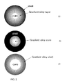
- FIG. 2 in a spherical nanocrystal structure of embodiments of the present invention, a corresponding alloy layer is shown in a gradient alloy structure, instead of a homogeneous alloy phase. See, for example, FIG. 2(a), (b), and (c) .
- FIG. 3 shows a structure of rod type interfused nanocrystals, according to embodiments of the present invention.
- a first rod, an alloy interlayer, and a second rod may be sequentially formed.
- the alloy interlayer may be in the form of a gradient alloy layer, instead of a homogenous alloy phase. See, for example, FIG. 3(b) .
- the alloy layer may be diffused up to the end of the first rod, thereby forming an alloy rod-second rod structure. See, for example, FIG. 3(c) .
- FIG. 4 shows a structure of tripod type interfused nanocrystals, according to embodiments of the present invention.
- a first rod, a second rod, and a third rod may be radially formed around a core, and an alloy interlayer may be formed at the interface of the core and the three rods.
- the alloy interlayer may be in the form of a gradient alloy layer, instead of a homogenous alloy phase. See, for example, FIG. 4(b) .
- a core rod, an alloy interlayer, and a shell rod may be formed.
- FIG. 5 shows a structure of tube type interfused nanocrystals, according to embodiments of the present invention.
- a core In the three-dimensional shapes of tubes, a core , an alloy interlayer, and a shell may be sequentially formed. See, for example, FIG. 5(a) .
- the alloy interlayer may be in the form of a gradient alloy layer, instead of a homogenous alloy phase. See, for example, FIG. 5(b) .
- an alloy core rod-shell structure or a core rodalloy shell structure may be formed by the diffusion of the alloy layer.
- the interfused nanocrystals may include a core, an alloy interlayer, and a shell, each of which is sequentially formed. Because the shell material or core material may diffuse into the adjacent core material or shell material, respectively, the actual size of a core for light emission decreases, and thus, an emission wavelength may be shifted into the blue light range. Even if a core having a relatively large size is used, it may emit light in the blue light range. The shift of the emission wavelength may result from the chemical composition of the core for emission varying with diffusion of the shell material or core material into the adjacent core material or shell material, respectively.
- the shell material has a wider band gap than the core, luminous efficiency in the blue light range may be drastically increased, by virtue of quantum confinement effects and passivation by the shell.
- the alloy layer which may be formed on the outer surface of the core, functions to decrease the difference in a lattice constant between the core and the shell and thereby increase the material stability.
- Each of the materials constituting the nanocrystals of embodiments of the present invention may be selected from the group consisting of Group II-VI semiconductor compounds, Group III-V semiconductor compounds, Group IV-VI semiconductor compounds, and mixtures thereof.
- materials constituting the nanocrystals may include, for example, CdS, CdSe, CdTe, ZnS, ZnSe, ZnTe, HgS, HgSe, HgTe, PbS, PbSe, PbTe, AIN, AIP, AlAs, GaN, GaP, GaAs, InN, InP, InAs, or mixtures thereof.
- each of the interfused nanocrystals may be selected from the group consisting of spheres, tetrahedra, cylinders, rods, triangles, discs, tripods, tetrapods, cubes, boxes, stars, and tubes, but is not limited thereto.
- CdSe//ZnS interfused nanocrystals according to embodiments of the present invention are represented by "CdSe//ZnS", which means a CdSe nanocrystal and a ZnS nanocrystal having an alloy interlayer therebetween.
- Another aspect of embodiments of the present invention pertains to a method of preparing the interfused nanocrystals.
- a method of preparing the interfused nanocrystals of embodiments of the present invention includes (a) forming a first nanocrystal, (b) growing a second nanocrystal comprising a material different from that of the first nanocrystal on the surface of the first nanocrystal obtained in (a), and (c) forming an alloy layer at an interface between the first nanocrystal and the second nanocrystal through diffusion.
- the formation of the first nanocrystal in (a) may be conducted by adding a metal precursor and a precursor of a Group V or VI compound to a solvent and a dispersant, and then mixing together to react.
- the formation of the second nanocrystal in (b) may be conducted by adding metal precursor and a precursor of a Group V or VI compound to a solvent and a dispersant, and then mixing together to react and grow on the first nanocrystal.
- the metal precursor and the precursor of a Group V or VI compound may be added to the solvent and the dispersant, and mixed together to react, to prepare a predetermined first nanocrystal.
- the first nanocrystal thus prepared may be added to a solution, containing precursors for a second nanocrystal in the solvent and the dispersant, and mixed together to react.
- the second nanocrystal may be grown on the surface of the first nanocrystal, and the alloy interlayer may be formed at the interface between the first nanocrystal and the second nanocrystal through diffusion.
- the alloy interlayer may be formed at the interface between the first nanocrystal and the second nanocrystal, through diffusion of the second nanocrystal material into the first nanocrystal material, or of the first nanocrystal material into the second nanocrystal material. Therefore, as one nanocrystal material diffuses into the other nanocrystal material, the amount of the one nanocrystal material is reduced, thus obtaining nanocrystals having a new structure comprising an alloy interlayer formed at an interface between the first nanocrystal and the second nanocrystal.
- Such an alloy layer may decrease the difference in a lattice constant of the materials constituting the nanocrystals, therefore increasing the material stability.
- a first nanocrystal-alloy layer structure or an alloy layer-second nanocrystal structure may be formed.
- (b) and (c) are repeatedly conducted once or more.
- the crystal growth reaction occurs on the surface of the second nanocrystal material to form another layer.
- the rod structure may be formed into tripods or tetrapods.
- the metal precursor used in (a) and (b) may include, for example, dimethyl zinc, diethyl zinc, zinc acetate, zinc acetylacetonate, zinc iodide, zinc bromide, zinc chloride, zinc fluoride, zinc carbonate, zinc cyanide, zinc nitrate, zinc oxide, zinc peroxide, zinc perchlorate, zinc sulfate, dimethyl cadmium, diethyl cadmium, cadmium acetate, cadmium acetylacetonate, cadmium iodide, cadmium bromide, cadmium chloride, cadmium fluoride, cadmium carbonate, cadmium nitrate, cadmium oxide, cadmium perchlorate, cadmium phosphide, cadmium sulfate, mercury acetate, mercury iod
- the Group V or VI compound used in (a) and (b) may include, for example, alkyl thiol compounds, such as hexanethiol, octanethiol, decanethiol, dodecanethiol, hexadecanethiol or mercaptopropylsilane, sulfur-trioctylphosphine (S-TOP), sulfur-tributylphosphine (S-TBP), sulfur-triphenylphosphine (S-TPP), sulfur-trioctylamine (S-TOA), trimethylsilyl sulfur, ammonium sulfide, sodium sulfide, selenium-trioctylphosphine (Se-TOP), selenium-tributylphosphine (Se-TBP), selenium-triphenylphosphine
- the concentration and rate of addition of the precursor be appropriately controlled depending on the reactivity of the precursor, so that undesired side-reactions, such as the separation of metal in the form of particles or the formation of additional particles by the reaction between the metal and the precursor of the Group V or VI compound, do not occur.
- the solvent used in (a) and (b) may include, for example, primary alkyl amines having 6 to 22 carbons, secondary alkyl amines having 6 to 22 carbons, and tertiary alkyl amines having 6 to 22 carbons; primary alcohols having 6 to 22 carbons, secondary alcohols having 6 to 22 carbons, and tertiary alcohols having 6 to 22 carbons; ketones and esters, either of which have 6 to 22 carbons; a heterocyclic compound including nitrogen or sulfur, which has 6 to 22 carbons; alkanes having 6 to 22 carbons, alkenes having 6 to 22 carbons, and alkynes having 6 to 22 carbons; trioctylphosphine; and trioctylphosphine oxide.
- the dispersant used in (a) and (b) may include, for example, alkanes or alkenes having 6 to 22 carbons and a COOH group at a terminal end thereof; alkanes or alkenes having 6 to 22 carbons and a POOH group at a terminal end thereof; alkanes or alkenes having 6 to 22 carbons and an SOOH group at a terminal end thereof; or alkanes or alkenes having 6 to 22 carbons and an NH 2 group at a terminal end thereof.
- the dispersant is exemplified by, but not limited to, oleic acid, stearic acid, palmitic acid, hexyl phosphonic acid, n-octyl phosphonic acid, tetradecyl phosphonic acid, octadecyl phosphonic acid, n-octyl amine, and hexadecyl amine.
- (a) and (b) may each be conducted at 100°C to 460°C, preferably 120°C to 390°C, and more preferably 150°C to 360°C, to assure the stability of the solvent while easily growing the crystals.
- (a) and (b) may each be conducted for a time period from 5 sec to 4 hr, preferably from 10 sec to 3 hr, and more preferably, from 20 sec to 2 hr, to easily control the reaction rate.
- the diffusion rate in (c) may be controlled by varying the reaction temperature, the reaction time, and the concentration of the metal precursor of the second nanocrystal in (b).
- the diffusion rate is controlled, therefore obtaining a material emitting light at a same wavelength.
- the diffusion rate in (c) may be controlled by stepwisely varying the reaction temperature in (b). Hence, even if a first nanocrystal having a consistent size is used, a material having a different emission wavelength may be obtained.
- the metal precursor used in (b) may have a concentration of 0.001 M to 2 M, and preferably 0.1 M to 1.6 M, to increase the luminous efficiency in the blue light wavelength range.
- the molar ratio of a metal precursor to a precursor of a Group V or VI compound used in (b) may range from 100:1 to 1:50, and preferably from 50:1 to 1:10, to increase the luminous efficiency in the blue light wavelength range.
- a further aspect of embodiments of the present invention pertains to interfused nanocrystals prepared using the above method.
- the shape of each of the nanocrystals may be selected from the group consisting of spheres, tetrahedra, cylinders, rods, triangles, discs, tripods, tetrapods, cubes, boxes, stars, and tubes, but is not limited thereto.
- the above nanocrystals may have an emission range from 350 nm to 700 nm, and preferably, from 380 nm to 490 nm and emit light with a maximum emission peak in the above range.
- the quantum efficiency of the nanocrystals is in the range of 0.1 % to 100%, and preferably, 20% to 100%.
- Interfused nanocrystals of embodiments of the present invention may be variously applied to displays, sensors, energy fields, etc., and, in particular, are useful in the formation of the light-emitting layer of a light-emitting diode for emitting blue light.
- Yet another aspect of embodiments of the present invention pertains to a diode including the interfused nanocrystals.
- a diode including the interfused nanocrystals may be provided.
- an organic-inorganic electrical light-emitting diode of embodiments of the present invention may comprise a substrate 10, a hole-injecting electrode 20, a hole-transporting layer 30, a light-emitting layer 40, an electron-transporting layer 50, and an electron-injecting layer 60, each of which is sequentially formed.
- the light-emitting layer 40 may include interfused semiconductor nanocrystals of embodiments of the present invention.
- Hole-transporting layer 30 and light-emitting layer 40 may be formed as a single layer. Also, electron-injecting layer 60 may be formed of two or more layers.
- a hole-inhibiting layer 70 may be selectively formed between the light-emitting layer 40 and the electron-transporting layer 50.
- the substrate 10 used in the electrical light-emitting diode of embodiments of the present invention may include commonly used substrates, for example, a glass substrate or a transparent plastic substrate, having excellent transparency, surface evenness, ease of handling and waterproofness. More particularly, it is exemplified by a glass substrate, a polyethyleneterephthalate substrate, or a polycarbonate substrate.
- a material for the hole-injecting electrode 20 may include conductive metals or oxides thereof, for example, ITO (Indium Tin Oxide), IZO (Indium Zinc Oxide), nickel (Ni), platinum (Pt), gold (Au), silver (Ag), iridium (Ir).
- ITO Indium Tin Oxide
- IZO Indium Zinc Oxide
- Ni nickel
- platinum Pt
- gold Au
- silver Au
- Ir iridium
- a material for the hole-transporting layer 30 may include all commonly used materials, for example, poly(3,4-ethylenediophene) (PEDOT)/polystyrene p-sulfonate (PSS), poly-N-vinylcarbazole derivatives, polyphenylenevinylene derivatives, polyparaphenylene derivatives, polymethacrylate derivatives, poly(9,9-octylfluorene) derivatives, poly(spiro-fluorene) derivatives, or TPD (N,N'-bis-(3-methylphenyl)-N,N'-bis-(phenyl)-benzidine), but is not limited thereto.
- the hole-transporting layer 30 of embodiments of the present invention is preferably 10 to 100 nm thick.
- a material for the electron-transporting layer 50 may include commonly used materials, for example, an oxazole compound, an iso-oxazole compound, a triazole compound, an iso-thiazole compound, an oxydiazole compound, a thiadiazole compound, a perylene compound, an aluminum complex, such as tris(8-hydroxyquinoline)-aluminum (Alq3), bis(2-methyl-8-quinolato)(p-phenylphenolato)aluminum (Balq), bis(2-methyl-8-quinolinato)(triphenylsiloxy)aluminum(III) (Salq), but is not limited thereto.
- the electron-transporting layer 50 is preferably 10 to 100 nm thick.
- a material for the electron-injecting electrode 60 may include metals having a low work function to easily inject an electron, for example, I, Ca, Ba, Ca/Al, LiF/Ca, LiF/Al, BaF2/Al, BaF2/Ca/Al, Al, Mg, Ag:Mg alloy, but is not limited thereto.
- the electron-injecting electrode 60 is preferably 50 to 300 nm thick.
- a material for the hole-inhibiting layer 70 may include materials commonly used in the art, for example, 3-(4-biphenylyl)-4-phenyl-5-(4- tert -butylphenyl)-1,2,4-triazole (TAZ), 2,9-dimethyl-1,10-phenanthroline (BCP), a phenanthroline compound, an imidazole compound, a triazole compound, an oxadiazole compound, an aluminum complex, but is not limited thereto.
- the hole-inhibiting layer 70 is preferably 5 to 50 nm thick.
- the nanocrystals thus obtained emitted blue light under a 365 nm UV lamp.
- the transmission electron micrograph of the interfused CdSe core and the CdSe//ZnS nanocrystals is shown in FIG. 6 and FIG. 7 , respectively.
- maximum emission peaks of the interfused CdSe//ZnS nanocrystals and the CdSe core appeared at 470 nm and 496 nm, respectively.
- the CdSe core had a maximum emission peak of 522 nm, and the interfused CdSe//ZnS nanocrystals emitted blue light at a wavelength that varied with the reaction temperature.
- the variation in emission peaks depending on the reaction temperature is summarized in Table 1, below.
- Table 1 Emission Wavelength of CdSe/Zns Synthesized at Different Reaction Temperatures using CdSe Core Emitting Light at 522 nm Reaction Temperature (°C) Emission Wavelength (nm) 220 498 260 476 300 440 320 442
- the nanocrystals thus obtained emitted blue light under a 365 nm UV lamp.
- the CdSe core had a maximum emission peak of 496 nm, and the interfused CdSe//ZnS nanocrystals emitted blue light at a wavelength that varied with the reaction time.
- the variation in emission peaks depending on the reaction time is summarized in Table 2, below.
- Table 2 Emission Wavelength of CdSe//ZnS Synthesized for Different Reaction Times using CdSe Core Emitting Light at 496 nm Reaction Time (min) Emission Wavelength (nm) 0 496 5 484 20 476 40 464 60 440
- the CdSe core had a maximum emission peak of 496 nm, and the interfused CdSe//ZnS nanocrystals emitted blue light at a wavelength that varied with the concentration of the precursor.
- the variation in emission peaks depending on the concentration of the precursor is summarized in Table 3, below.
- Table 3 Emission Wavelength of CdSe/rZns Synthesized at Different Precursor Concentrations for 30 min using CdSe Core Emitting Light at 496 nm Concentration of Zn Precursor in Synthesized Solution (mM) Emission Wavelength (nm) 4 474 20 468 40 459
- a photoluminescence spectra showing the excited light emission spectrum of the CdSe solution used as a core, the nanocrystal solution obtained through the reaction at 260°C for 1 hr, and the nanocrystal solution obtained through the reaction at 260°C for 1 hr and then 300°C for 1 hr, is shown in FIG. 9 .
- maximum emission peaks appeared at 498, 492 and 466 nm, respectively.
- the nanocrystals thus obtained emitted blue light under a 365 nm UV lamp.
- a photoluminescence spectra, showing the excited light emission spectrum of the above nanocrystal solution and the CdSe core, is shown in FIG. 10 .
- reaction mixture was cooled down to room temperature rapidly, and ethanol was added as a non-solvent. After centrifuging the obtained reaction solution, the supernatant of the solution was decanted, with the exception of the centrifuged precipitate, and the precipitate was dispersed in toluene to obtain a 1 wt% solution, to prepare a CdSeS nanocrystal solution.
- the nanocrystals thus obtained emitted blue light under a 365 nm UV lamp.
- a photoluminescence spectrum, showing the excited light emission spectrum of the above nanocrystal solution and the CdSeS core, is shown in FIG. 11 .
- the present example is a preparative example of manufacturing an organic-inorganic hybrid electrical light emitting diode using the CdSe//ZnS nanocrystals prepared in Example 1 as a light emitting material of the electrical light emitting diode.
- a chloroform solution of 3 wt% N,N'-bis-(3-methylphenyl)-N,N'-bis-(phenyl)-benzidine (TPD) serving as a hole transporting material and a chloroform solution of 1 wt% CdSe//ZnS prepared in Example 1 were mixed and spin-coated on a patterned ITO layer, and then dried, to form a single hole transporting and light emitting layer.
- 3-(4-biphenylyl)-4-phenyl-5-(4- tert -butylphenyl)-1,2,4-triazole (TAZ) was deposited to a thickness of 10 nm, to form a hole inhibiting layer, on which tris-(8-hydroxyquinoline)aluminum (Alq 3 ) serving as an electron transporting layer was deposited to a thickness of 30 nm.
- LiF was deposited to a thickness of 1 nm on the electron transporting layer, after which aluminum was deposited to a thickness of 200 nm to form a cathode, thereby completing an electrical light emitting diode.
- the structure of the organic-inorganic hybrid electrical light emitting diode thus manufactured is shown in FIG. 12 , and the electrical light emitting spectrum thereof is shown in FIG. 13 .
- the emission peak was about 470 nm
- FWHM was about 36 nm
- brightness was 500 Cd/m 2
- the efficiency of the device was 1.5 Cd/A.
- embodiments of the present invention provide interfused nanocrystals and a method of preparing the interfused nanocrystals.
- Interfused nanocrystals of embodiments of the present invention have an alloy layer between different crystals, thus increasing the material stability. Further, material having very excellent light emitting efficiency in the blue light range may be prepared.
Landscapes
- Chemical & Material Sciences (AREA)
- Engineering & Computer Science (AREA)
- Organic Chemistry (AREA)
- Crystallography & Structural Chemistry (AREA)
- Nanotechnology (AREA)
- Physics & Mathematics (AREA)
- Materials Engineering (AREA)
- Optics & Photonics (AREA)
- Inorganic Chemistry (AREA)
- Metallurgy (AREA)
- General Physics & Mathematics (AREA)
- Condensed Matter Physics & Semiconductors (AREA)
- Life Sciences & Earth Sciences (AREA)
- Biophysics (AREA)
- Composite Materials (AREA)
- Luminescent Compositions (AREA)
- Electroluminescent Light Sources (AREA)
- Manufacture Of Metal Powder And Suspensions Thereof (AREA)
- Powder Metallurgy (AREA)
- Led Devices (AREA)
Applications Claiming Priority (3)
| Application Number | Priority Date | Filing Date | Title |
|---|---|---|---|
| KR20040091894 | 2004-11-11 | ||
| KR1020050079284A KR100722086B1 (ko) | 2004-11-11 | 2005-08-29 | 다층구조의 나노결정 및 그의 제조방법 |
| EP05256775.7A EP1666562B1 (fr) | 2004-11-11 | 2005-11-02 | Nanocristaux fusionné et méthode de leur préparation |
Related Parent Applications (2)
| Application Number | Title | Priority Date | Filing Date |
|---|---|---|---|
| EP05256775.7 Division | 2005-11-02 | ||
| EP05256775.7A Division-Into EP1666562B1 (fr) | 2004-11-11 | 2005-11-02 | Nanocristaux fusionné et méthode de leur préparation |
Publications (2)
| Publication Number | Publication Date |
|---|---|
| EP2292718A2 true EP2292718A2 (fr) | 2011-03-09 |
| EP2292718A3 EP2292718A3 (fr) | 2011-06-22 |
Family
ID=35998502
Family Applications (2)
| Application Number | Title | Priority Date | Filing Date |
|---|---|---|---|
| EP05256775.7A Expired - Lifetime EP1666562B1 (fr) | 2004-11-11 | 2005-11-02 | Nanocristaux fusionné et méthode de leur préparation |
| EP10186278A Withdrawn EP2292718A3 (fr) | 2004-11-11 | 2005-11-02 | Nanocristaux fusionné et méthode de leur préparation |
Family Applications Before (1)
| Application Number | Title | Priority Date | Filing Date |
|---|---|---|---|
| EP05256775.7A Expired - Lifetime EP1666562B1 (fr) | 2004-11-11 | 2005-11-02 | Nanocristaux fusionné et méthode de leur préparation |
Country Status (3)
| Country | Link |
|---|---|
| US (2) | US20060236918A1 (fr) |
| EP (2) | EP1666562B1 (fr) |
| JP (1) | JP4800006B2 (fr) |
Cited By (10)
| Publication number | Priority date | Publication date | Assignee | Title |
|---|---|---|---|---|
| CN108269928A (zh) * | 2016-12-30 | 2018-07-10 | Tcl集团股份有限公司 | 一种正置底发射qled器件及其制备方法 |
| CN108269933A (zh) * | 2016-12-30 | 2018-07-10 | Tcl集团股份有限公司 | 一种反置底发射qled器件及其制备方法 |
| CN108269929A (zh) * | 2016-12-30 | 2018-07-10 | Tcl集团股份有限公司 | 一种正置顶发射qled器件及其制备方法 |
| CN108269927A (zh) * | 2016-12-30 | 2018-07-10 | Tcl集团股份有限公司 | 一种反置顶发射qled器件及其制备方法 |
| CN108264900A (zh) * | 2016-12-30 | 2018-07-10 | Tcl集团股份有限公司 | 一种量子点复合材料、制备方法及半导体器件 |
| CN108269892A (zh) * | 2016-12-30 | 2018-07-10 | Tcl集团股份有限公司 | 具有量子阱能级结构的合金材料、制备方法及半导体器件 |
| CN108269926A (zh) * | 2016-12-30 | 2018-07-10 | Tcl集团股份有限公司 | 一种量子点组成及其制备方法 |
| US20190006607A1 (en) * | 2016-12-30 | 2019-01-03 | Tcl Corporation | Quantum dot material, preparation method, and semiconductor device |
| US20190085238A1 (en) * | 2017-09-21 | 2019-03-21 | Raytheon Company | Process for producing quantum dots having broadened optical emission |
| US11168252B2 (en) | 2016-12-30 | 2021-11-09 | Tcl Technology Group Corporation | Quantum dot material, preparation method, and semiconductor device |
Families Citing this family (57)
| Publication number | Priority date | Publication date | Assignee | Title |
|---|---|---|---|---|
| GB2441699B (en) * | 2005-05-14 | 2011-04-06 | Atmos | Metal oxide particles for use as semiconductor materials and methods of producing them |
| WO2007086188A1 (fr) * | 2006-01-30 | 2007-08-02 | Konica Minolta Medical & Graphic, Inc. | Nanoparticule semi-conductrice triple couche et nanotige semi-conductrice triple couche |
| WO2007143197A2 (fr) | 2006-06-02 | 2007-12-13 | Qd Vision, Inc. | Dispositifs émetteurs de lumière et affichages à performances ameliorées |
| JPWO2007145089A1 (ja) * | 2006-06-14 | 2009-10-29 | コニカミノルタエムジー株式会社 | 3層型半導体粒子 |
| KR100901947B1 (ko) * | 2006-07-14 | 2009-06-10 | 삼성전자주식회사 | 반도체 나노결정을 이용하는 백색 발광 다이오드 및 그의제조방법 |
| JP2010508620A (ja) * | 2006-09-12 | 2010-03-18 | キユーデイー・ビジヨン・インコーポレーテツド | 所定のパターンを表示するために有用なエレクトロルミネセントディスプレイ |
| WO2008063657A2 (fr) * | 2006-11-21 | 2008-05-29 | Qd Vision, Inc. | Dispositifs luminescents et afficheurs à performance améliorée |
| WO2008133660A2 (fr) | 2006-11-21 | 2008-11-06 | Qd Vision, Inc. | Nanocristaux comprenant un élément du groupe iiia et un élément du groupe va, composition, dispositif et autres produits |
| JP5151993B2 (ja) * | 2007-01-22 | 2013-02-27 | コニカミノルタエムジー株式会社 | コア/シェル型半導体ナノ粒子とその製造方法 |
| JP4528985B2 (ja) * | 2007-02-07 | 2010-08-25 | 国立大学法人 筑波大学 | ZnPd系微粒子およびその製造方法 |
| KR100841186B1 (ko) | 2007-03-26 | 2008-06-24 | 삼성전자주식회사 | 다층 쉘 구조의 나노결정 및 그의 제조방법 |
| JP5773646B2 (ja) | 2007-06-25 | 2015-09-02 | キユーデイー・ビジヨン・インコーポレーテツド | ナノ材料を被着させることを含む組成物および方法 |
| US8361823B2 (en) * | 2007-06-29 | 2013-01-29 | Eastman Kodak Company | Light-emitting nanocomposite particles |
| JP5710255B2 (ja) * | 2007-09-12 | 2015-04-30 | キユーデイー・ビジヨン・インコーポレーテツド | 官能化ナノ粒子および方法 |
| US20100289003A1 (en) * | 2007-10-29 | 2010-11-18 | Kahen Keith B | Making colloidal ternary nanocrystals |
| US7777233B2 (en) * | 2007-10-30 | 2010-08-17 | Eastman Kodak Company | Device containing non-blinking quantum dots |
| WO2009081918A1 (fr) * | 2007-12-26 | 2009-07-02 | Idemitsu Kosan Co., Ltd. | Élément électroluminescent organique/inorganique hybride |
| JP2009176730A (ja) | 2007-12-28 | 2009-08-06 | Sumitomo Chemical Co Ltd | 高分子発光素子、製造方法及び高分子発光ディスプレイ装置 |
| JP5019052B2 (ja) * | 2007-12-28 | 2012-09-05 | 独立行政法人放射線医学総合研究所 | CdSe量子ドット及びその製造方法 |
| US9748422B2 (en) | 2008-01-23 | 2017-08-29 | Massachusetts Institute Of Technology | Semiconductor nanocrystals |
| US9525148B2 (en) | 2008-04-03 | 2016-12-20 | Qd Vision, Inc. | Device including quantum dots |
| KR20110008206A (ko) | 2008-04-03 | 2011-01-26 | 큐디 비젼, 인크. | 양자점들을 포함하는 발광 소자 |
| KR100973172B1 (ko) * | 2008-08-05 | 2010-08-02 | 한국과학기술연구원 | 단일 활성층 구조를 가지는 교류 구동형 발광소자 및 그제조방법 |
| JP5170469B2 (ja) * | 2010-02-25 | 2013-03-27 | 国立大学法人 筑波大学 | ZnPd系微粒子およびその製造方法 |
| KR101664180B1 (ko) * | 2010-03-22 | 2016-10-12 | 삼성디스플레이 주식회사 | 양자점 제조 방법 |
| JP5744468B2 (ja) * | 2010-10-20 | 2015-07-08 | シャープ株式会社 | 半導体ナノ粒子蛍光体 |
| WO2013058900A1 (fr) * | 2011-10-18 | 2013-04-25 | Eastman Kodak Company | Nanocristaux semi-conducteurs hautement confinés |
| US8784703B2 (en) | 2011-10-18 | 2014-07-22 | Eastman Kodak Company | Method of making highly-confined semiconductor nanocrystals |
| US20130112942A1 (en) | 2011-11-09 | 2013-05-09 | Juanita Kurtin | Composite having semiconductor structures embedded in a matrix |
| US20130112941A1 (en) | 2011-11-09 | 2013-05-09 | Juanita Kurtin | Semiconductor structure having nanocrystalline core and nanocrystalline shell with insulator coating |
| US9103009B2 (en) | 2012-07-04 | 2015-08-11 | Apple Inc. | Method of using core shell pre-alloy structure to make alloys in a controlled manner |
| US10752514B2 (en) | 2012-09-07 | 2020-08-25 | Cornell University | Metal chalcogenide synthesis method and applications |
| US20140117311A1 (en) | 2012-10-29 | 2014-05-01 | Juanita N. Kurtin | Semiconductor structure having nanocrystalline core and nanocrystalline shell pairing with compositional transition layer |
| CN104099095A (zh) * | 2013-04-09 | 2014-10-15 | 海洋王照明科技股份有限公司 | 钕镱共掺杂氟化锡玻璃上转换发光材料、制备方法及其应用 |
| KR102164628B1 (ko) | 2013-08-05 | 2020-10-13 | 삼성전자주식회사 | 나노 결정 합성 방법 |
| KR20160102394A (ko) * | 2013-10-17 | 2016-08-30 | 나노포토니카, 인크. | 빛 방출을 위한 양자점 및 이의 합성방법 |
| US10065396B2 (en) | 2014-01-22 | 2018-09-04 | Crucible Intellectual Property, Llc | Amorphous metal overmolding |
| US11205757B2 (en) | 2014-11-06 | 2021-12-21 | Sn Display Co., Ltd. | Core-shell structured perovskite particle light-emitter, method of preparing the same and light emitting device using the same |
| CN105153807B (zh) * | 2015-07-21 | 2016-10-19 | 京东方科技集团股份有限公司 | 量子点墨水 |
| CN105070848B (zh) | 2015-09-11 | 2017-06-16 | 上海天马有机发光显示技术有限公司 | 显示面板、有机发光器件及其制备方法 |
| EP3405550B1 (fr) * | 2016-01-19 | 2021-04-21 | Nanosys, Inc. | Procédé pour fabriquer points quantiques en inp avec coques en gap et alp |
| CN105800952A (zh) * | 2016-02-28 | 2016-07-27 | 桂林理工大学 | 一种CdSe纳米晶光电材料的制备方法 |
| CN108269930B (zh) | 2016-12-30 | 2020-05-26 | Tcl科技集团股份有限公司 | 一种合金纳米材料、制备方法及半导体器件 |
| US10096743B1 (en) * | 2017-05-26 | 2018-10-09 | Unique Materials Co., Ltd. | Gigantic quantum dots |
| EP3733812B1 (fr) * | 2017-12-29 | 2024-02-28 | TCL Technology Group Corporation | Point quantique, son procédé de préparation et son utilisation |
| CN110028963B (zh) | 2018-01-11 | 2024-01-02 | 三星电子株式会社 | 量子点、量子点-聚合物复合物、和显示装置 |
| EP3753651A4 (fr) | 2018-02-13 | 2021-12-15 | Murata Manufacturing Co., Ltd. | Structure magnétique |
| US12108615B2 (en) * | 2018-08-21 | 2024-10-01 | Georgia Tech Research Corporation | Infrared-emitting quantum dots and methods for making same |
| US11262584B2 (en) | 2018-10-25 | 2022-03-01 | Facebook Technologies, Llc | Color foveated display devices and methods of making the same |
| WO2020174604A1 (fr) * | 2019-02-27 | 2020-09-03 | シャープ株式会社 | Élément électroluminescent et dispositif d'affichage l'utilisant |
| KR102888211B1 (ko) | 2019-12-20 | 2025-11-21 | 삼성디스플레이 주식회사 | 양자점 조성물의 제조 방법 및 이를 포함하는 발광 소자의 제조 방법 |
| WO2021152720A1 (fr) * | 2020-01-29 | 2021-08-05 | シャープ株式会社 | Élément électroluminescent et procédé de production d'élément électroluminescent |
| TWI811582B (zh) * | 2020-11-09 | 2023-08-11 | 優美特創新材料股份有限公司 | 高穩定性半導體奈米材料 |
| CN114695749A (zh) * | 2020-12-31 | 2022-07-01 | Tcl科技集团股份有限公司 | 光电器件 |
| KR102597304B1 (ko) | 2021-01-18 | 2023-11-02 | 주식회사 신아티앤씨 | 코어-쉘 구조 양자점 입자의 제조방법, 이에 의해 제조된 코어-쉘 구조 양자점 입자, 상기 코어-쉘 구조 양자점 입자 집단 및 이를 포함하는 디스플레이장치 |
| CN119278677A (zh) * | 2022-07-19 | 2025-01-07 | 夏普显示科技株式会社 | 发光元件、显示装置、发光元件的制造方法以及发光元件的发光特性的恢复方法 |
| WO2024062628A1 (fr) * | 2022-09-22 | 2024-03-28 | シャープディスプレイテクノロジー株式会社 | Élément électroluminescent, dispositif d'affichage et procédé de production d'élément électroluminescent |
Citations (4)
| Publication number | Priority date | Publication date | Assignee | Title |
|---|---|---|---|---|
| US6207229B1 (en) | 1997-11-13 | 2001-03-27 | Massachusetts Institute Of Technology | Highly luminescent color-selective materials and method of making thereof |
| WO2002025745A2 (fr) * | 2000-09-14 | 2002-03-28 | Yissum Research Development Company Of The Hebrew University Of Jerusalem | Materiaux nanocristallins semi-conducteurs et leurs utilisations |
| US20030039860A1 (en) * | 2001-08-16 | 2003-02-27 | Cheon Jin Woo | Method for synthesis of core-shell type and solid solution alloy type metallic nanoparticles via transmetalation reactions and applications of same |
| WO2003092043A2 (fr) * | 2001-07-20 | 2003-11-06 | Quantum Dot Corporation | Nanoparticules luminescentes et techniques de preparation |
Family Cites Families (17)
| Publication number | Priority date | Publication date | Assignee | Title |
|---|---|---|---|---|
| US6607829B1 (en) * | 1997-11-13 | 2003-08-19 | Massachusetts Institute Of Technology | Tellurium-containing nanocrystalline materials |
| US7496670B1 (en) * | 1997-11-20 | 2009-02-24 | Amdocs (Israel) Ltd. | Digital asset monitoring system and method |
| CA2306814A1 (fr) * | 1997-11-20 | 1999-06-03 | Xacct Technologies, Inc. | Systeme d'imputation comptable et de comptabilisation des transactions reseau, et procede correspondant |
| US6797412B1 (en) * | 2000-04-11 | 2004-09-28 | University Of Connecticut | Full color display structures using pseudomorphic cladded quantum dot nanophosphor thin films |
| WO2002100805A2 (fr) * | 2001-06-13 | 2002-12-19 | University Of Rochester | Detecteurs a nanocristaux colorimetriques, procedes de fabrication et utilisation associee |
| US20030066998A1 (en) * | 2001-08-02 | 2003-04-10 | Lee Howard Wing Hoon | Quantum dots of Group IV semiconductor materials |
| US6710366B1 (en) * | 2001-08-02 | 2004-03-23 | Ultradots, Inc. | Nanocomposite materials with engineered properties |
| ATE448077T1 (de) * | 2001-09-17 | 2009-11-15 | Life Technologies Corp | Nanokristalle |
| US20030066938A1 (en) * | 2001-10-09 | 2003-04-10 | Zimmerman Arlen J. | Light string bracket |
| FR2838241B1 (fr) * | 2002-04-09 | 2004-06-25 | Commissariat Energie Atomique | Materiaux luminescents constitues de nanocristaux a structure coeur/coquille et leur procede de preparation |
| EP1537263B1 (fr) * | 2002-08-13 | 2010-11-17 | Massachusetts Institute Of Technology | Heterostructures de nanocristaux de semi-conducteur |
| US7534488B2 (en) * | 2003-09-10 | 2009-05-19 | The Regents Of The University Of California | Graded core/shell semiconductor nanorods and nanorod barcodes |
| US7056471B1 (en) * | 2002-12-16 | 2006-06-06 | Agency For Science Technology & Research | Ternary and quarternary nanocrystals, processes for their production and uses thereof |
| WO2004066361A2 (fr) * | 2003-01-22 | 2004-08-05 | The Board Of Trustees Of The University Of Arkansas | Nanocristaux a noyau/enveloppe monodisperses et autres nanocristaux structures complexes et leurs procedes de preparation |
| EP1627420B1 (fr) * | 2003-05-07 | 2020-07-15 | Indiana University Research and Technology Corporation | Points quantiques a alliage de semi-conducteurs et points quantiques a alliage a gradient de concentration, series comprenant ces points quantiques et procedes associes |
| KR100796122B1 (ko) * | 2003-09-09 | 2008-01-21 | 삼성전자주식회사 | 화합물 반도체 나노결정의 표면 처리를 통한 양자효율 향상 |
| US7253452B2 (en) * | 2004-03-08 | 2007-08-07 | Massachusetts Institute Of Technology | Blue light emitting semiconductor nanocrystal materials |
-
2005
- 2005-11-02 EP EP05256775.7A patent/EP1666562B1/fr not_active Expired - Lifetime
- 2005-11-02 EP EP10186278A patent/EP2292718A3/fr not_active Withdrawn
- 2005-11-07 JP JP2005322668A patent/JP4800006B2/ja not_active Expired - Lifetime
- 2005-11-09 US US11/269,685 patent/US20060236918A1/en not_active Abandoned
-
2007
- 2007-07-09 US US11/822,677 patent/US8247795B2/en active Active
Patent Citations (5)
| Publication number | Priority date | Publication date | Assignee | Title |
|---|---|---|---|---|
| US6207229B1 (en) | 1997-11-13 | 2001-03-27 | Massachusetts Institute Of Technology | Highly luminescent color-selective materials and method of making thereof |
| US6322901B1 (en) | 1997-11-13 | 2001-11-27 | Massachusetts Institute Of Technology | Highly luminescent color-selective nano-crystalline materials |
| WO2002025745A2 (fr) * | 2000-09-14 | 2002-03-28 | Yissum Research Development Company Of The Hebrew University Of Jerusalem | Materiaux nanocristallins semi-conducteurs et leurs utilisations |
| WO2003092043A2 (fr) * | 2001-07-20 | 2003-11-06 | Quantum Dot Corporation | Nanoparticules luminescentes et techniques de preparation |
| US20030039860A1 (en) * | 2001-08-16 | 2003-02-27 | Cheon Jin Woo | Method for synthesis of core-shell type and solid solution alloy type metallic nanoparticles via transmetalation reactions and applications of same |
Cited By (20)
| Publication number | Priority date | Publication date | Assignee | Title |
|---|---|---|---|---|
| US20220064528A1 (en) * | 2016-12-30 | 2022-03-03 | Tcl Technology Group Corporation | Quantum dot composite material, preparation method, and semiconductor device |
| CN108269933A (zh) * | 2016-12-30 | 2018-07-10 | Tcl集团股份有限公司 | 一种反置底发射qled器件及其制备方法 |
| CN108269929A (zh) * | 2016-12-30 | 2018-07-10 | Tcl集团股份有限公司 | 一种正置顶发射qled器件及其制备方法 |
| CN108269927A (zh) * | 2016-12-30 | 2018-07-10 | Tcl集团股份有限公司 | 一种反置顶发射qled器件及其制备方法 |
| CN108264900A (zh) * | 2016-12-30 | 2018-07-10 | Tcl集团股份有限公司 | 一种量子点复合材料、制备方法及半导体器件 |
| CN108269892A (zh) * | 2016-12-30 | 2018-07-10 | Tcl集团股份有限公司 | 具有量子阱能级结构的合金材料、制备方法及半导体器件 |
| CN108269926A (zh) * | 2016-12-30 | 2018-07-10 | Tcl集团股份有限公司 | 一种量子点组成及其制备方法 |
| US20190006607A1 (en) * | 2016-12-30 | 2019-01-03 | Tcl Corporation | Quantum dot material, preparation method, and semiconductor device |
| US11795394B2 (en) | 2016-12-30 | 2023-10-24 | Tcl Technology Group Corporation | Quantum dot composite material, preparation method, and semiconductor device |
| US20190071603A1 (en) * | 2016-12-30 | 2019-03-07 | Tcl Corporation | Quantum dot composite material, preparation method, and semiconductor device |
| US11121338B2 (en) * | 2016-12-30 | 2021-09-14 | Tcl Technology Group Corporation | Quantum dot material, preparation method, and semiconductor device |
| CN108269892B (zh) * | 2016-12-30 | 2021-06-22 | Tcl科技集团股份有限公司 | 具有量子阱能级结构的合金材料、制备方法及半导体器件 |
| US11746293B2 (en) * | 2016-12-30 | 2023-09-05 | Tcl Technology Group Corporation | Quantum dot composite material, preparation method, and semiconductor device |
| US11168252B2 (en) | 2016-12-30 | 2021-11-09 | Tcl Technology Group Corporation | Quantum dot material, preparation method, and semiconductor device |
| US11203715B2 (en) * | 2016-12-30 | 2021-12-21 | Tcl Technology Group Corporation | Quantum dot composite material, preparation method, and semiconductor device |
| CN108269928A (zh) * | 2016-12-30 | 2018-07-10 | Tcl集团股份有限公司 | 一种正置底发射qled器件及其制备方法 |
| US20220064530A1 (en) * | 2016-12-30 | 2022-03-03 | Tcl Technology Group Corporation | Quantum dot composite material, preparation method, and semiconductor device |
| US11746292B2 (en) * | 2016-12-30 | 2023-09-05 | Tcl Technology Group Corporation | Quantum dot composite material, preparation method, and semiconductor device |
| US10711188B2 (en) * | 2017-09-21 | 2020-07-14 | Raytheon Company | Process for producing quantum dots having broadened optical emission |
| US20190085238A1 (en) * | 2017-09-21 | 2019-03-21 | Raytheon Company | Process for producing quantum dots having broadened optical emission |
Also Published As
| Publication number | Publication date |
|---|---|
| JP2006186317A (ja) | 2006-07-13 |
| EP1666562A2 (fr) | 2006-06-07 |
| JP4800006B2 (ja) | 2011-10-26 |
| US8247795B2 (en) | 2012-08-21 |
| US20060236918A1 (en) | 2006-10-26 |
| EP1666562A3 (fr) | 2007-06-13 |
| EP1666562B1 (fr) | 2018-03-07 |
| EP2292718A3 (fr) | 2011-06-22 |
| US20080029760A1 (en) | 2008-02-07 |
Similar Documents
| Publication | Publication Date | Title |
|---|---|---|
| EP1666562B1 (fr) | Nanocristaux fusionné et méthode de leur préparation | |
| US10577716B2 (en) | Multilayer nanocrystal structure and method for producing the same | |
| US10202545B2 (en) | Interfused nanocrystals and method of preparing the same | |
| JP5602104B2 (ja) | 多層構造のナノ結晶およびその製造方法 | |
| US8247073B2 (en) | Core-shell nanocrystal comprising a non-semiconductor buffer layer, method for preparing the same and electronic device comprising the same | |
| US7658905B2 (en) | Method of preparing cadmium sulfide nanocrystals emitting light at multiple wavelengths, and cadmium sulfide nanocrystals prepared by the method | |
| US7455825B2 (en) | Method for manufacturing metal sulfide nanocrystals using thiol compound as sulfur precursor | |
| KR101738551B1 (ko) | 반도체 나노 결정 | |
| CN101208808B (zh) | 蓝光发射半导体纳米晶体材料 | |
| EP3760692B1 (fr) | Boites quantiques émettant dans le rouge ayant une largeur totale étroite à mi-hauteur et longueur d'onde d'émission pour application à un affichage à grande pureté de couleurs, et leur procédé de préparation | |
| KR101981975B1 (ko) | 청색 발광 양자점 및 제조방법 | |
| US7850943B2 (en) | Method of preparing cadmium sulfide nanocrystals emitting light at multiple wavelengths, and cadmium sulfide nanocrystals prepared by the method | |
| KR102866636B1 (ko) | 양자점, 양자점 제조방법 및 전자소자 | |
| US20250248178A1 (en) | PRODUCTION METHOD OF SEMICONDUCTOR NANOPARTICLE, and ELECTROLUMINESCENT DEVICE INCLUDING THE SEMICONDUCTOR NANOPARTICLE |
Legal Events
| Date | Code | Title | Description |
|---|---|---|---|
| PUAI | Public reference made under article 153(3) epc to a published international application that has entered the european phase |
Free format text: ORIGINAL CODE: 0009012 |
|
| AC | Divisional application: reference to earlier application |
Ref document number: 1666562 Country of ref document: EP Kind code of ref document: P |
|
| AK | Designated contracting states |
Kind code of ref document: A2 Designated state(s): DE FR GB |
|
| PUAL | Search report despatched |
Free format text: ORIGINAL CODE: 0009013 |
|
| AK | Designated contracting states |
Kind code of ref document: A3 Designated state(s): DE FR GB |
|
| 17P | Request for examination filed |
Effective date: 20111221 |
|
| 17Q | First examination report despatched |
Effective date: 20120229 |
|
| RAP1 | Party data changed (applicant data changed or rights of an application transferred) |
Owner name: SAMSUNG ELECTRONICS CO., LTD. |
|
| GRAP | Despatch of communication of intention to grant a patent |
Free format text: ORIGINAL CODE: EPIDOSNIGR1 |
|
| INTG | Intention to grant announced |
Effective date: 20170109 |
|
| STAA | Information on the status of an ep patent application or granted ep patent |
Free format text: STATUS: THE APPLICATION IS DEEMED TO BE WITHDRAWN |
|
| 18D | Application deemed to be withdrawn |
Effective date: 20170520 |