EP2291867B1 - Verfahren zum vereinzeln von silizium-solarzellen - Google Patents
Verfahren zum vereinzeln von silizium-solarzellen Download PDFInfo
- Publication number
- EP2291867B1 EP2291867B1 EP10719944A EP10719944A EP2291867B1 EP 2291867 B1 EP2291867 B1 EP 2291867B1 EP 10719944 A EP10719944 A EP 10719944A EP 10719944 A EP10719944 A EP 10719944A EP 2291867 B1 EP2291867 B1 EP 2291867B1
- Authority
- EP
- European Patent Office
- Prior art keywords
- silicon wafer
- laser beam
- solar cells
- groove
- cutting
- Prior art date
- Legal status (The legal status is an assumption and is not a legal conclusion. Google has not performed a legal analysis and makes no representation as to the accuracy of the status listed.)
- Not-in-force
Links
Images

Classifications
-
- H—ELECTRICITY
- H10—SEMICONDUCTOR DEVICES; ELECTRIC SOLID-STATE DEVICES NOT OTHERWISE PROVIDED FOR
- H10F—INORGANIC SEMICONDUCTOR DEVICES SENSITIVE TO INFRARED RADIATION, LIGHT, ELECTROMAGNETIC RADIATION OF SHORTER WAVELENGTH OR CORPUSCULAR RADIATION
- H10F71/00—Manufacture or treatment of devices covered by this subclass
- H10F71/121—The active layers comprising only Group IV materials
-
- B—PERFORMING OPERATIONS; TRANSPORTING
- B23—MACHINE TOOLS; METAL-WORKING NOT OTHERWISE PROVIDED FOR
- B23K—SOLDERING OR UNSOLDERING; WELDING; CLADDING OR PLATING BY SOLDERING OR WELDING; CUTTING BY APPLYING HEAT LOCALLY, e.g. FLAME CUTTING; WORKING BY LASER BEAM
- B23K26/00—Working by laser beam, e.g. welding, cutting or boring
- B23K26/02—Positioning or observing the workpiece, e.g. with respect to the point of impact; Aligning, aiming or focusing the laser beam
- B23K26/06—Shaping the laser beam, e.g. by masks or multi-focusing
- B23K26/062—Shaping the laser beam, e.g. by masks or multi-focusing by direct control of the laser beam
- B23K26/0622—Shaping the laser beam, e.g. by masks or multi-focusing by direct control of the laser beam by shaping pulses
-
- B—PERFORMING OPERATIONS; TRANSPORTING
- B23—MACHINE TOOLS; METAL-WORKING NOT OTHERWISE PROVIDED FOR
- B23K—SOLDERING OR UNSOLDERING; WELDING; CLADDING OR PLATING BY SOLDERING OR WELDING; CUTTING BY APPLYING HEAT LOCALLY, e.g. FLAME CUTTING; WORKING BY LASER BEAM
- B23K26/00—Working by laser beam, e.g. welding, cutting or boring
- B23K26/36—Removing material
- B23K26/362—Laser etching
- B23K26/364—Laser etching for making a groove or trench, e.g. for scribing a break initiation groove
-
- B—PERFORMING OPERATIONS; TRANSPORTING
- B23—MACHINE TOOLS; METAL-WORKING NOT OTHERWISE PROVIDED FOR
- B23K—SOLDERING OR UNSOLDERING; WELDING; CLADDING OR PLATING BY SOLDERING OR WELDING; CUTTING BY APPLYING HEAT LOCALLY, e.g. FLAME CUTTING; WORKING BY LASER BEAM
- B23K26/00—Working by laser beam, e.g. welding, cutting or boring
- B23K26/36—Removing material
- B23K26/40—Removing material taking account of the properties of the material involved
-
- B—PERFORMING OPERATIONS; TRANSPORTING
- B23—MACHINE TOOLS; METAL-WORKING NOT OTHERWISE PROVIDED FOR
- B23K—SOLDERING OR UNSOLDERING; WELDING; CLADDING OR PLATING BY SOLDERING OR WELDING; CUTTING BY APPLYING HEAT LOCALLY, e.g. FLAME CUTTING; WORKING BY LASER BEAM
- B23K2103/00—Materials to be soldered, welded or cut
- B23K2103/50—Inorganic materials other than metals or composite materials
-
- Y—GENERAL TAGGING OF NEW TECHNOLOGICAL DEVELOPMENTS; GENERAL TAGGING OF CROSS-SECTIONAL TECHNOLOGIES SPANNING OVER SEVERAL SECTIONS OF THE IPC; TECHNICAL SUBJECTS COVERED BY FORMER USPC CROSS-REFERENCE ART COLLECTIONS [XRACs] AND DIGESTS
- Y02—TECHNOLOGIES OR APPLICATIONS FOR MITIGATION OR ADAPTATION AGAINST CLIMATE CHANGE
- Y02E—REDUCTION OF GREENHOUSE GAS [GHG] EMISSIONS, RELATED TO ENERGY GENERATION, TRANSMISSION OR DISTRIBUTION
- Y02E10/00—Energy generation through renewable energy sources
- Y02E10/50—Photovoltaic [PV] energy
- Y02E10/547—Monocrystalline silicon PV cells
-
- Y—GENERAL TAGGING OF NEW TECHNOLOGICAL DEVELOPMENTS; GENERAL TAGGING OF CROSS-SECTIONAL TECHNOLOGIES SPANNING OVER SEVERAL SECTIONS OF THE IPC; TECHNICAL SUBJECTS COVERED BY FORMER USPC CROSS-REFERENCE ART COLLECTIONS [XRACs] AND DIGESTS
- Y02—TECHNOLOGIES OR APPLICATIONS FOR MITIGATION OR ADAPTATION AGAINST CLIMATE CHANGE
- Y02P—CLIMATE CHANGE MITIGATION TECHNOLOGIES IN THE PRODUCTION OR PROCESSING OF GOODS
- Y02P70/00—Climate change mitigation technologies in the production process for final industrial or consumer products
- Y02P70/50—Manufacturing or production processes characterised by the final manufactured product
Definitions
- the invention relates to a method for separating silicon solar cells.
- the invention is therefore based on the object to provide a method for separating silicon solar cells, with which the above-mentioned disadvantages are avoided.
- a groove is introduced which has a depth reaching at least to the pn junction and extends to a lateral edge of the silicon wafer.
- the silicon wafer is placed on the groove directed second laser beam cut along the dividing line, wherein the melting material formed during cutting is expelled with a cutting gas flowing at least approximately in the direction of the second laser beam from the cutting groove formed during cutting.
- the groove extends at least as far as a depth of the silicon wafer in which the pn junction is located, at least laser melting in the melting zone results in a melt containing p-dopant. Since this is expelled towards the back of the silicon wafer, this can not attach to the n-doped side wall of the groove. As a result, a short-circuiting of the silicon solar cell arising at the edge can be avoided.
- first and second laser beams are pulsed, wherein the pulse duration of the first laser beam is shorter than the pulse duration of the second laser beam.
- First and second laser beam can be generated by two different lasers as well as by a laser, which can work in correspondingly different modes.
- a plurality of finished silicon silicon solar cells 4 are arranged in a silicon wafer 2, which are separated from each other in a subsequent, explained below manufacturing step at predetermined separation lines 5, ie isolated.
- the silicon wafer 2 is made up of a p-doped silicon substrate 6 serving as a base, which is provided on a rear side 8 with a metallic base contact 10.
- a p-doped silicon substrate 6 serving as a base
- an n-doped emitter layer 12 has been produced by adding an n-dopant on the front side 14 opposite the rear side 8, which is only a few microns thick, so that in a depth T only a few microns dashed line pn junction 16 is located.
- the front side 14 of the silicon wafer 2 is also provided with an antireflection layer 18 and with a plurality of emitter contacts 20.
- a groove 22 is introduced (incised) in a first working step with a first laser beam L1 along one of the separating lines 5 by a laser ablation or laser ablation process into the front side 14 of the silicon wafer 2 adjacent to the pn junction 16, whose depth t extends at least to the depth T of the pn-junction 16, which is typically about 1 micron.
- the removal begins at a lateral edge 24 of the silicon wafer 2.
- the removal can, however, in principle also begin at a location spaced from the edge of the silicon wafer 2. It is essential, however, that the finished groove 22 extends to the lateral edges 24 of the silicon wafer 2.
- the first laser beam L1 is pulsed, wherein the pulse durations are preferably in the nanosecond range and wavelengths in the range between 200nm - 2000nm are used. In principle, shorter pulse durations are also suitable, which are below the nanosecond range.
- the depth t of the groove 22 in this case preferably exceeds the depth t of the pn junction by several micrometers, for example by more than 10 ⁇ m. In practice, a depth of the groove 22 of about 12-15 ⁇ m has been found to be suitable
- the substrate 2 After completion of the groove 22 is in accordance with 4 and 5 the substrate 2 in a second step with a directed into the groove 22 second, preferably also pulsed laser beam L2 beginning at the lateral edge 24 along the dividing line 5 cut.
- the pulse durations of the second laser beam L2 are typically in the microsecond range, wherein the wavelength of the second laser beam L2 is preferably in the near infrared range.
- the kerf 28 reaches the rear side 8, so that a separating gap which opens towards the rear 8 and spreads out by advancing the laser beam L2 in the direction of the parting line 5 arises, from which the melt M can be expelled towards the back 8. In this way, the pn junction on the side walls of the separation gap is maintained.
Landscapes
- Physics & Mathematics (AREA)
- Optics & Photonics (AREA)
- Engineering & Computer Science (AREA)
- Plasma & Fusion (AREA)
- Mechanical Engineering (AREA)
- Photovoltaic Devices (AREA)
- Laser Beam Processing (AREA)
Abstract
Description
- Die Erfindung bezieht sich auf ein Verfahren zum Vereinzeln von Silizium-Solarzellen.
- Bei der Herstellung von Silizium-Solarzellen werden in einem Siliziumwafer in der Regel eine große Anzahl einzelner Silizium-Solarzellen hergestellt, die in einem abschließenden Fertigungsschritt vereinzelt, d.h. voneinander getrennt werden müssen. Im Stand der Technik erfolgt dies entweder mit einem mechanischen Sägeverfahren oder mit einem beispielsweise aus der
WO 2008/084206 A1 bekannten Laserschneidverfahren. Das Dokument R. Mayerhafer et al., Photvoltaic Energy Conversion, Conference Record of the 2006 IEEE 4th World Conference on, IEEE, PI Mai 2006, Seiten 1115-1118 beschreibt ein Verfahren zum Vereinzeln von Solarzellen. Werden diese Verfahren einstufig durchgeführt, d.h. erfolgt eine Trennung in einem einzigen Prozessschritt, so kann es vorkommen, dass die einzelnen Silizium-Solarzellen insbesondere beim Laserschneiden kurzgeschlossen werden. Ursache hierfür ist, dass in der Schneidfuge eine Schmelzzone entsteht, die mit Dotierungselementen angereichert sein kann. Dadurch kann am Rand der Schneidfuge eine Zone entstehen, in der die Dotierungselemente vermischt sind und der pn-Übergang zerstört ist. Dies kann zu einem Kurzschluss zwischen der Vorderseite, d.h. der Flachseite der Solarzelle, in deren Nähe sich der pn-Übergang befindet, und der Rückseite führen. Dieses Problem tritt sowohl beim konventionellen Laserschneiden, bei dem mit einem in die Schneidfuge mit hoher Geschwindigkeit einströmenden Schneidgas die Schmelze ausgetrieben wird, als auch beim einstufigen Laserschneiden mit einem Laserablationsverfahren auf, bei dem das Material in erster Linie durch Verdampfen aus der Schneidfuge entweicht, und bei dem in der Regel ein güte-geschalteter Festkörperlaser eingesetzt wird. Auch beim mechanischen Trennen durch Sägen ist ein solcher Kurzschluss nicht ausgeschlossen, da der metallische Kontakt an der Rückseite der Silizium-Solarzelle ebenfalls an den Schnittflächen verschmiert wird. - Um dieses Problem zu vermeiden, ist es bekannt, beim Vereinzeln von Silizium-Solarzellen einen zweistufigen Prozess einzusetzen, bei dem im ersten Schritt mit einem Laserstrahl eine Nut in den Siliziumwafer eingebracht und anschließend der Siliziumwafer entlang dieser Nuten mechanisch aufgebrochen wird.
- Das anschließende Brechen des Siliziumwafers erfordert aber einen zusätzlichen Prozessschritt mit einer anderen Fertigungstechnik. Außerdem können beim Aufbrechen einzelne Silizium-Solarzellen zerstört werden.
- Der Erfindung liegt daher die Aufgabe zu Grunde, ein Verfahren zum Vereinzeln von Silizium-Solarzellen anzugeben, mit dem die vorstehend genannten Nachteile vermieden sind.
- Die genannte Aufgabe wird gemäß der Erfindung gelöst mit einem Verfahren mit den Merkmalen des Patentanspruches 1. Bei diesem Verfahren wird in einem ersten Arbeitsschritt in einen die Silizium-Solarzellen enthaltenden Siliziumwafer mit einem ersten Laserstrahl entlang einer Trennlinie in eine einem pn-Übergang im Siliziumwafer benachbarte Vorderseite des Siliziumwafers eine Nut eingebracht, die eine zumindest bis zum pn-Übergang reichende Tiefe aufweist und sich bis zu einem seitlichen Rand des Siliziumwafers erstreckt. In einem zweiten Arbeitsschritt wird der Siliziumwafer mit einem auf die Nut gerichtete zweiten Laserstrahl entlang der Trennlinie geschnitten, wobei das während des Schneidens entstehende Schmelzgut mit einem zumindest annähernd in Richtung des zweiten Laserstrahls strömenden Schneidgas aus der beim Schneiden entstehenden Schneidfuge ausgetrieben wird.
- Da sich die Nut zumindest bis in eine Tiefe des Siliziumwafers erstreckt, in der sich der pn-Übergang befindet, entsteht beim Laserschneiden in der Schmelzzone allenfalls ein p-Dotierstoff enthaltendes Schmelzgut. Da dieses in Richtung zur Rückseite des Siliziumwafers ausgetrieben wird, kann sich dieses nicht an der n-dotierten Seitenwand der Nut anlagern. Dadurch kann ein am Rand entstehender Kurzschluss der Silizium-Solarzelle vermieden werden.
- Besonders gute Ergebnisse werden erzielt, wenn sowohl erster als auch zweiter Laserstrahl gepulst sind, wobei die Pulsdauer des ersten Laserstrahls kürzer ist als die Pulsdauer des zweiten Laserstrahls. Erster und zweiter Laserstrahl können dabei sowohl von zwei unterschiedlichen Lasern als auch von einem Laser erzeugt werden, der in entsprechend unterschiedlichen Betriebsarten arbeiten kann.
- Zur weiteren Erläuterung der Erfindung wird auf das Ausführungsbeispiel der Zeichnung verwiesen. Es zeigen:
-
Fig.1 einen eine Mehrzahl von Silizium-Solarzellen enthaltenden Siliziumwafer in einer schematischen Draufsicht auf eine seiner Flachseiten, -
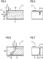
Fig. 2 ,4 und 6 jeweils einen Silizium-Solarzellen enthaltenden Siliziumwafer an einem seiner Ränder in einem Längsschnitt entlang einer Trennlinie während der Durchführung des ersten Arbeitsschrittes, am Beginn des zweiten Arbeitsschrittes bzw. während dem Durchführen des zweiten Arbeitsschrittes, -
Fig. 3 ,5 und 7 den zu denFig. 1, 3 und5 jeweils korrespondierenden Arbeitsschritt in einer Draufsicht in Richtung der Trennlinie auf eine Schmalseite des Siliziumwafers. - Gemäß
Fig. 1 sind in einem Siliziumwafer 2 eine Mehrzahl fertig prozessierter Silizium-Solarzellen 4 angeordnet, die in einem anschließenden, nachfolgend erläuterten Fertigungsschritt an vorgegebenen Trennlinien 5 voneinander getrennt, d.h. vereinzelt werden. - Gemäß
Fig. 2 und 3 ist der Siliziumwafer 2 aus einem als Basis dienenden p-dotierten Siliziumsubstrat 6 aufgebaut, das auf einer Rückseite 8 mit einem metallischem Basiskontakt 10 versehen ist. In dem p-dotierten Siliziumsubstrat 6 ist durch Zugabe eines n-Dotierstoffes auf der der Rückseite 8 gegenüberliegenden Vorderseite 14 eine n-dotierte Emitterschicht 12 hergestellt worden, die nur wenige µm dick ist, so dass sich in einer nur wenige µm betragenden Tiefe T ein gestrichelt eingezeichneter pn-Übergang 16 befindet. Die Vorderseite 14 des Siliziumwafers 2 ist außerdem mit einer Antireflexionsschicht 18 sowie mit einer Mehrzahl von Emitterkontakten 20 versehen. - Zum Vereinzeln der Silizium-Solarzellen 4 wird in einem ersten Arbeitsschritt mit einem ersten Laserstrahl L1 entlang einer der Trennlinien 5 durch ein Laserabtrags- bzw. Laserablationsverfahren in die dem pn-Übergang 16 benachbarte Vorderseite 14 des Siliziumwafers 2 eine Nut 22 eingebracht (eingeritzt), deren Tiefe t sich zumindest bis zur Tiefe T des pn-Überganges 16, die typisch etwa 1 µm beträgt erstreckt. Im Beispiel der
Fig. 2 und 3 beginnt der Abtrag an einem seitlichen Rand 24 des Siliziumwafers 2. Der Abtrag kann aber grundsätzlich auch an einer vom Rand des Siliziumwafers 2 beabstandeten Stelle beginnen. Wesentlich ist aber, dass sich die fertiggestellte Nut 22 bis zu den seitlichen Rändern 24 des Siliziumwafers 2 erstreckt. Der erste Laserstrahl L1 ist gepulst, wobei die Pulsdauern vorzugsweise im Nanosekundenbereich liegen und Wellenlängen im Bereich zwischen 200nm - 2000nm verwendet werden. Grundsätzlich sind auch kürzere Pulsdauern geeignet, die unterhalb des Nanosekundenbereichs liegen. Die Tiefe t der Nut 22 überschreitet dabei die Tiefe t des pn-Überganges vorzugsweise um mehrere Mikrometer, beispielsweise um mehr als 10µm. In der Praxis hat sich eine Tiefe der Nut 22 von etwa 12-15µm als geeignet herausgestellt - Nach Fertigstellen der Nut 22 wird gemäß
Fig. 4 und 5 das Substrat 2 in einem zweiten Arbeitsschritt mit einem in die Nut 22 gerichteten zweiten, vorzugsweise ebenfalls gepulsten Laserstrahl L2 beginnend am seitlichen Rand 24 entlang der Trennlinie 5 geschnitten. Dabei wird das während des Laserschneidens entstehende Schmelzgut M mit einem annähernd in Richtung des zweiten Laserstrahls L2 mit hoher Geschwindigkeit strömenden Schneidgas G aus einer am Beginn des Laserschneidens entstehenden und noch nicht bis zur Rückseite 8 reichenden Schneidfuge 28 seitlich am Rand 24, d.h. mit einer in Richtung des zweiten Laserstrahls L2 orientierten, zur Rückseite hin gerichteten Strömungskomponente ausgetrieben. Auf diese Weise wird verhindert, dass sich beim Aufschmelzen der Basis, d.h. des p-dotierten Bereiches des Siliziumsubstrates 6 eine mit p-Dotierstoff angereicherte Schmelzzone ausbildet, die sich bis zur n-dotierten Seitenwand der Nut 22 ausbreitet und diese benetzt. Mit anderen Worten: Das mit p-Dotierstoffen angereicherte Schmelzgut M kommt nicht in Kontakt mit der n-dotierten Emitterschicht 12. Die Pulsdauern des zweiten Laserstrahls L2 liegen typisch im Mikrosekundenbereich, wobei die Wellenlänge des zweiten Laserstrahls L2 vorzugsweise im nahen Infrarotbereich liegt. - Gemäß
Fig. 6 und 7 erreicht die Schneidfuge 28 die Rückseite 8, so dass ein zur Rückseite 8 hin offener und sich durch Vorschub des Laserstahls L2 in Richtung der Trennlinie 5 ausbreitender Trennspalt entsteht, aus dem das Schmelzgut M zur Rückseite 8 hin ausgetrieben werden kann. Auf diese Weise bleibt der pn-Übergang an den Seitenwänden des Trennspaltes erhalten.
Claims (2)
- Verfahren zum Vereinzeln von Silizium-Solarzellen (4), bei dem in einem ersten Arbeitsschritt in einen die Silizium-Solarzellen (4) enthaltenden Siliziumwafer (2) mit einem ersten Laserstrahl (L1) entlang einer Trennlinie (5) in eine einem pn-Übergang (16) im Siliziumwafer (2) benachbarte Vorderseite (14) des Siliziumwafers (2) eine Nut (22) eingebracht wird, die eine zumindest bis zum pn-Übergang (16) reichende Tiefe (t) aufweist und sich bis zu einem seitlichen Rand (24) des Siliziumwafers (2) erstreckt, und bei dem in einem zweiten Arbeitsschritt der Siliziumwafer (2) mit einem in die Nut (22) gerichteten zweiten Laserstrahl (L2) beginnend am seitlichen Rand (24) entlang der Trennlinie (5) geschnitten wird, wobei das während des Schneidens entstehende Schmelzgut (M) mit einem zumindest annähernd in Richtung des zweiten Laserstrahls (L2) strömenden Schneidgas (G) aus der beim Schneiden entstehenden Schneidfuge (28) ausgetrieben wird.
- Verfahren nach Anspruch 1, bei dem erster und zweiter Laserstrahl gepulst sind, wobei die Pulsdauer des ersten Laserstrahls kürzer ist als die Pulsdauer des zweiten Laserstrahls (L2).
Applications Claiming Priority (2)
| Application Number | Priority Date | Filing Date | Title |
|---|---|---|---|
| DE102009026410A DE102009026410A1 (de) | 2009-05-20 | 2009-05-20 | Verfahren zum Vereinzeln von Silizium-Solarzellen |
| PCT/EP2010/056708 WO2010133536A1 (de) | 2009-05-20 | 2010-05-17 | Verfahren zum vereinzeln von silizium-solarzellen |
Publications (2)
| Publication Number | Publication Date |
|---|---|
| EP2291867A1 EP2291867A1 (de) | 2011-03-09 |
| EP2291867B1 true EP2291867B1 (de) | 2012-05-16 |
Family
ID=42309524
Family Applications (1)
| Application Number | Title | Priority Date | Filing Date |
|---|---|---|---|
| EP10719944A Not-in-force EP2291867B1 (de) | 2009-05-20 | 2010-05-17 | Verfahren zum vereinzeln von silizium-solarzellen |
Country Status (5)
| Country | Link |
|---|---|
| US (1) | US20110124147A1 (de) |
| EP (1) | EP2291867B1 (de) |
| JP (1) | JP5462936B2 (de) |
| DE (1) | DE102009026410A1 (de) |
| WO (1) | WO2010133536A1 (de) |
Families Citing this family (16)
| Publication number | Priority date | Publication date | Assignee | Title |
|---|---|---|---|---|
| DE102011012275A1 (de) * | 2011-02-24 | 2012-08-30 | Ritek Corp. | Verfahren zum Schneiden eines Solarzellenpanels und Ausrüstung dafür |
| DE102012214335A1 (de) * | 2012-08-10 | 2014-02-13 | Fraunhofer-Gesellschaft zur Förderung der angewandten Forschung e.V. | Verfahren zur Ablation einer Schicht |
| DE102012217766B4 (de) * | 2012-09-28 | 2016-06-16 | Trumpf Werkzeugmaschinen Gmbh + Co. Kg | Verfahren und Vorrichtung zum Dampfdruck-Abtragschneiden eines metallischen Werkstücks |
| EP2905814B1 (de) * | 2012-10-02 | 2020-04-01 | Kaneka Corporation | Verfahren zur herstellung einer kristallinen siliciumsolarzelle, und verfahren zur herstellung eines solarzellenmoduls |
| JP2014194977A (ja) * | 2013-03-28 | 2014-10-09 | Kaneka Corp | 結晶シリコン系太陽電池およびその製造方法 |
| JP6181979B2 (ja) * | 2013-05-29 | 2017-08-16 | 株式会社カネカ | 太陽電池およびその製造方法、ならびに太陽電池モジュール |
| JP6313086B2 (ja) * | 2014-03-27 | 2018-04-18 | 株式会社カネカ | 結晶シリコン太陽電池およびその製造方法、太陽電池モジュールの製造方法、集光型太陽電池モジュールの製造方法 |
| US9776906B2 (en) * | 2014-03-28 | 2017-10-03 | Electro Scientific Industries, Inc. | Laser machining strengthened glass |
| DE102018123485B4 (de) * | 2018-09-24 | 2021-04-08 | Fraunhofer-Gesellschaft zur Förderung der angewandten Forschung e.V. | Verfahren zum Auftrennen eines Halbleiterbauelements mit einem pn-Übergang |
| DE102018123484A1 (de) * | 2018-09-24 | 2020-03-26 | Fraunhofer-Gesellschaft zur Förderung der angewandten Forschung e.V. | Verfahren zum Vereinzeln eines Halbleiterbauelementes mit einem pn-Übergang und Halbleiterbauelement mit einem pn-Übergang |
| EP3965990B1 (de) | 2019-05-08 | 2024-09-11 | WSoptics technologies GmbH | Verfahren und strahlbearbeitungsvorrichtung zur strahlbearbeitung eines werkstücks |
| US12062733B2 (en) | 2019-06-04 | 2024-08-13 | Jusung Engineering Co., Ltd. | Substrate for solar cell, solar cell, and solar cell manufacturing method |
| WO2021094481A1 (en) * | 2019-11-13 | 2021-05-20 | Nederlandse Organisatie Voor Toegepast-Natuurwetenschappelijk Onderzoek Tno | Method for creating shunt free translucent flexible thin-film photovoltaic module |
| CN113555463A (zh) * | 2020-04-23 | 2021-10-26 | 苏州阿特斯阳光电力科技有限公司 | 太阳能电池的制备方法与太阳能电池 |
| US11764315B2 (en) * | 2020-09-16 | 2023-09-19 | Maxeon Solar Pte. Ltd. | Solar cell separation with edge coating |
| CN112054096A (zh) * | 2020-09-29 | 2020-12-08 | 天合光能股份有限公司 | 一种切片单晶硅电池的制备方法 |
Family Cites Families (13)
| Publication number | Priority date | Publication date | Assignee | Title |
|---|---|---|---|---|
| JPH07120646B2 (ja) * | 1990-05-16 | 1995-12-20 | 株式会社東芝 | メサ型半導体ペレットの製造方法 |
| DE19624677A1 (de) * | 1996-06-20 | 1998-01-02 | Siemens Ag | Verfahren zur Vereinzelung von optoelektrischen Bauelementen |
| JP3516156B2 (ja) * | 1997-12-16 | 2004-04-05 | シャープ株式会社 | 太陽電池の製造方法および保護カバー用素材板 |
| US6420245B1 (en) * | 1999-06-08 | 2002-07-16 | Kulicke & Soffa Investments, Inc. | Method for singulating semiconductor wafers |
| JP4786010B2 (ja) * | 2000-03-23 | 2011-10-05 | 株式会社カネカ | 集積型ハイブリッド薄膜太陽電池の製造方法 |
| JP2003151921A (ja) * | 2001-11-09 | 2003-05-23 | Sanyo Electric Co Ltd | 化合物半導体とその製造方法 |
| JP2005523583A (ja) * | 2002-04-19 | 2005-08-04 | エグシル テクノロジー リミテッド | パルスレーザを用いる、基板のプログラム制御ダイシング |
| GB2402230B (en) * | 2003-05-30 | 2006-05-03 | Xsil Technology Ltd | Focusing an optical beam to two foci |
| JP4369259B2 (ja) * | 2004-02-19 | 2009-11-18 | シャープ株式会社 | 太陽電池セルの製造方法 |
| JP2006027025A (ja) * | 2004-07-14 | 2006-02-02 | Seiko Epson Corp | 基板の切断方法、および半導体チップの製造方法 |
| JP4439477B2 (ja) * | 2005-03-29 | 2010-03-24 | 三洋電機株式会社 | 光起電力素子及びその製造方法 |
| JP4717545B2 (ja) * | 2005-08-01 | 2011-07-06 | シャープ株式会社 | 光電変換素子の製造方法 |
| WO2008084206A1 (en) * | 2007-01-08 | 2008-07-17 | Spi Lasers Uk Limited | A process for laser cutting a non-metallic material |
-
2009
- 2009-05-20 DE DE102009026410A patent/DE102009026410A1/de not_active Withdrawn
-
2010
- 2010-05-17 WO PCT/EP2010/056708 patent/WO2010133536A1/de not_active Ceased
- 2010-05-17 EP EP10719944A patent/EP2291867B1/de not_active Not-in-force
- 2010-05-17 JP JP2012511246A patent/JP5462936B2/ja active Active
-
2011
- 2011-02-04 US US13/020,972 patent/US20110124147A1/en not_active Abandoned
Also Published As
| Publication number | Publication date |
|---|---|
| JP2012527753A (ja) | 2012-11-08 |
| DE102009026410A1 (de) | 2011-03-17 |
| WO2010133536A1 (de) | 2010-11-25 |
| JP5462936B2 (ja) | 2014-04-02 |
| US20110124147A1 (en) | 2011-05-26 |
| EP2291867A1 (de) | 2011-03-09 |
Similar Documents
| Publication | Publication Date | Title |
|---|---|---|
| WO2010133536A1 (de) | Verfahren zum vereinzeln von silizium-solarzellen | |
| DE102004024643B4 (de) | Werkstückteilungsverfahren unter Verwendung eines Laserstrahls | |
| EP1924392B1 (de) | Verfahren zum durchtrennen von spröden flachmaterialien mittels laser entlang einer zuvor erzeugten spur | |
| DE602004012999T2 (de) | Fokussierung eines optischen strahles auf zwei fokusse | |
| DE102006000720B4 (de) | Laserstrahlbearbeitungsmaschine | |
| DE102013221822B4 (de) | Chip mit Rückseitenmetall und Verfahren zu seiner Herstellung und Halbleiterscheibe mit Rückseitenmetall | |
| DE112007001278T5 (de) | Infrarotlaser-Waferritzen unter Verwendung von kurzen Impulsen | |
| WO2015010706A1 (de) | Verfahren und vorrichtung zur trennung eines flachen werkstücks in mehrere teilstücke | |
| DE102004055443A1 (de) | Waferbearbeitungsverfahren | |
| DE102007049553B4 (de) | Laserbearbeitungsverfahren für Galliumarsenid-Wafer | |
| DE102013105426A1 (de) | Verfahren zum Laserritzen einer Solarzelle | |
| WO2011060764A2 (de) | Emitterbildung mit einem laser | |
| EP3356078A1 (de) | Verfahren zur herstellung eines metall-keramik substrates mit picolaser | |
| DE3617141A1 (de) | Halbleiterbaueinheit mit integrierter schaltung und schmelzsicherungsstrecke | |
| DE102018102108B4 (de) | Verfahren zum laserbasierten Erzeugen einer Struktur an einer Spanfläche eines spanenden Werkzeugs | |
| DE112016004420T5 (de) | Laserbearbeitungsverfahren und laserbearbeitungsvorrichtung | |
| EP2177302B1 (de) | Verfahren zum Abtragen von Schichtmaterial eines Schichtaufbaus mittels Laserstrahlung mit einem Hilfsgrabenschritt und einem Abtragschritt | |
| EP3787044B1 (de) | Vereinzelungsverfahren zur vereinzelung einer mehrere solarzellenstapel umfassenden halbleiterscheibe | |
| DE10326505B4 (de) | Laserritzen von Dünnschichthalbleiterbauelementen | |
| DE102015118042A1 (de) | Verfahren und Vorrichtung zum Herstellen einer Halbleiterschicht | |
| DE102010020974A1 (de) | Verfahren zum Herstellen von Spezialsolarzellen aus einem Wafer | |
| EP4388593A1 (de) | Verfahren zum vereinzeln von halbleiterbauelementen | |
| DE102012216740B4 (de) | Silizium-Solarzelle, die durch Zerteilen einer auf einem Silizium-Wafer ausgebildeten Ausgangssolarzelle erzeugt ist, Photovoltaikmodul und Verfahren zur Herstellung einer Solarzelle | |
| DE102009026411A1 (de) | Verfahren zum Vereinzeln von Dünnschichtsolarzellen | |
| EP3192135B1 (de) | Verfahren zum herstellen eines laserchips |
Legal Events
| Date | Code | Title | Description |
|---|---|---|---|
| PUAI | Public reference made under article 153(3) epc to a published international application that has entered the european phase |
Free format text: ORIGINAL CODE: 0009012 |
|
| 17P | Request for examination filed |
Effective date: 20101221 |
|
| AK | Designated contracting states |
Kind code of ref document: A1 Designated state(s): AL AT BE BG CH CY CZ DE DK EE ES FI FR GB GR HR HU IE IS IT LI LT LU LV MC MK MT NL NO PL PT RO SE SI SK SM TR |
|
| AX | Request for extension of the european patent |
Extension state: BA ME RS |
|
| GRAP | Despatch of communication of intention to grant a patent |
Free format text: ORIGINAL CODE: EPIDOSNIGR1 |
|
| GRAS | Grant fee paid |
Free format text: ORIGINAL CODE: EPIDOSNIGR3 |
|
| GRAA | (expected) grant |
Free format text: ORIGINAL CODE: 0009210 |
|
| AK | Designated contracting states |
Kind code of ref document: B1 Designated state(s): AL AT BE BG CH CY CZ DE DK EE ES FI FR GB GR HR HU IE IS IT LI LT LU LV MC MK MT NL NO PL PT RO SE SI SK SM TR |
|
| DAX | Request for extension of the european patent (deleted) | ||
| REG | Reference to a national code |
Ref country code: GB Ref legal event code: FG4D Free format text: NOT ENGLISH |
|
| REG | Reference to a national code |
Ref country code: CH Ref legal event code: EP |
|
| REG | Reference to a national code |
Ref country code: AT Ref legal event code: REF Ref document number: 558445 Country of ref document: AT Kind code of ref document: T Effective date: 20120615 |
|
| REG | Reference to a national code |
Ref country code: IE Ref legal event code: FG4D Free format text: LANGUAGE OF EP DOCUMENT: GERMAN |
|
| REG | Reference to a national code |
Ref country code: DE Ref legal event code: R096 Ref document number: 502010000764 Country of ref document: DE Effective date: 20120712 |
|
| REG | Reference to a national code |
Ref country code: NL Ref legal event code: VDEP Effective date: 20120516 |
|
| REG | Reference to a national code |
Ref country code: LT Ref legal event code: MG4D Effective date: 20120516 |
|
| PG25 | Lapsed in a contracting state [announced via postgrant information from national office to epo] |
Ref country code: PL Free format text: LAPSE BECAUSE OF FAILURE TO SUBMIT A TRANSLATION OF THE DESCRIPTION OR TO PAY THE FEE WITHIN THE PRESCRIBED TIME-LIMIT Effective date: 20120516 Ref country code: NO Free format text: LAPSE BECAUSE OF FAILURE TO SUBMIT A TRANSLATION OF THE DESCRIPTION OR TO PAY THE FEE WITHIN THE PRESCRIBED TIME-LIMIT Effective date: 20120816 Ref country code: IS Free format text: LAPSE BECAUSE OF FAILURE TO SUBMIT A TRANSLATION OF THE DESCRIPTION OR TO PAY THE FEE WITHIN THE PRESCRIBED TIME-LIMIT Effective date: 20120916 Ref country code: LT Free format text: LAPSE BECAUSE OF FAILURE TO SUBMIT A TRANSLATION OF THE DESCRIPTION OR TO PAY THE FEE WITHIN THE PRESCRIBED TIME-LIMIT Effective date: 20120516 Ref country code: SE Free format text: LAPSE BECAUSE OF FAILURE TO SUBMIT A TRANSLATION OF THE DESCRIPTION OR TO PAY THE FEE WITHIN THE PRESCRIBED TIME-LIMIT Effective date: 20120516 Ref country code: FI Free format text: LAPSE BECAUSE OF FAILURE TO SUBMIT A TRANSLATION OF THE DESCRIPTION OR TO PAY THE FEE WITHIN THE PRESCRIBED TIME-LIMIT Effective date: 20120516 Ref country code: CY Free format text: LAPSE BECAUSE OF FAILURE TO SUBMIT A TRANSLATION OF THE DESCRIPTION OR TO PAY THE FEE WITHIN THE PRESCRIBED TIME-LIMIT Effective date: 20120516 |
|
| BERE | Be: lapsed |
Owner name: ROFIN-BAASEL LASERTECH G.M.B.H. & CO. KG Effective date: 20120531 |
|
| PG25 | Lapsed in a contracting state [announced via postgrant information from national office to epo] |
Ref country code: SI Free format text: LAPSE BECAUSE OF FAILURE TO SUBMIT A TRANSLATION OF THE DESCRIPTION OR TO PAY THE FEE WITHIN THE PRESCRIBED TIME-LIMIT Effective date: 20120516 Ref country code: GR Free format text: LAPSE BECAUSE OF FAILURE TO SUBMIT A TRANSLATION OF THE DESCRIPTION OR TO PAY THE FEE WITHIN THE PRESCRIBED TIME-LIMIT Effective date: 20120817 Ref country code: HR Free format text: LAPSE BECAUSE OF FAILURE TO SUBMIT A TRANSLATION OF THE DESCRIPTION OR TO PAY THE FEE WITHIN THE PRESCRIBED TIME-LIMIT Effective date: 20120516 Ref country code: PT Free format text: LAPSE BECAUSE OF FAILURE TO SUBMIT A TRANSLATION OF THE DESCRIPTION OR TO PAY THE FEE WITHIN THE PRESCRIBED TIME-LIMIT Effective date: 20120917 Ref country code: LV Free format text: LAPSE BECAUSE OF FAILURE TO SUBMIT A TRANSLATION OF THE DESCRIPTION OR TO PAY THE FEE WITHIN THE PRESCRIBED TIME-LIMIT Effective date: 20120516 |
|
| PG25 | Lapsed in a contracting state [announced via postgrant information from national office to epo] |
Ref country code: MC Free format text: LAPSE BECAUSE OF NON-PAYMENT OF DUE FEES Effective date: 20120531 |
|
| PG25 | Lapsed in a contracting state [announced via postgrant information from national office to epo] |
Ref country code: SK Free format text: LAPSE BECAUSE OF FAILURE TO SUBMIT A TRANSLATION OF THE DESCRIPTION OR TO PAY THE FEE WITHIN THE PRESCRIBED TIME-LIMIT Effective date: 20120516 Ref country code: EE Free format text: LAPSE BECAUSE OF FAILURE TO SUBMIT A TRANSLATION OF THE DESCRIPTION OR TO PAY THE FEE WITHIN THE PRESCRIBED TIME-LIMIT Effective date: 20120516 Ref country code: RO Free format text: LAPSE BECAUSE OF FAILURE TO SUBMIT A TRANSLATION OF THE DESCRIPTION OR TO PAY THE FEE WITHIN THE PRESCRIBED TIME-LIMIT Effective date: 20120516 Ref country code: CZ Free format text: LAPSE BECAUSE OF FAILURE TO SUBMIT A TRANSLATION OF THE DESCRIPTION OR TO PAY THE FEE WITHIN THE PRESCRIBED TIME-LIMIT Effective date: 20120516 Ref country code: DK Free format text: LAPSE BECAUSE OF FAILURE TO SUBMIT A TRANSLATION OF THE DESCRIPTION OR TO PAY THE FEE WITHIN THE PRESCRIBED TIME-LIMIT Effective date: 20120516 Ref country code: NL Free format text: LAPSE BECAUSE OF FAILURE TO SUBMIT A TRANSLATION OF THE DESCRIPTION OR TO PAY THE FEE WITHIN THE PRESCRIBED TIME-LIMIT Effective date: 20120516 |
|
| REG | Reference to a national code |
Ref country code: IE Ref legal event code: MM4A |
|
| PG25 | Lapsed in a contracting state [announced via postgrant information from national office to epo] |
Ref country code: MK Free format text: LAPSE BECAUSE OF FAILURE TO SUBMIT A TRANSLATION OF THE DESCRIPTION OR TO PAY THE FEE WITHIN THE PRESCRIBED TIME-LIMIT Effective date: 20120516 Ref country code: BE Free format text: LAPSE BECAUSE OF NON-PAYMENT OF DUE FEES Effective date: 20120531 Ref country code: IT Free format text: LAPSE BECAUSE OF FAILURE TO SUBMIT A TRANSLATION OF THE DESCRIPTION OR TO PAY THE FEE WITHIN THE PRESCRIBED TIME-LIMIT Effective date: 20120516 |
|
| PLBE | No opposition filed within time limit |
Free format text: ORIGINAL CODE: 0009261 |
|
| STAA | Information on the status of an ep patent application or granted ep patent |
Free format text: STATUS: NO OPPOSITION FILED WITHIN TIME LIMIT |
|
| REG | Reference to a national code |
Ref country code: FR Ref legal event code: ST Effective date: 20130307 |
|
| 26N | No opposition filed |
Effective date: 20130219 |
|
| PG25 | Lapsed in a contracting state [announced via postgrant information from national office to epo] |
Ref country code: ES Free format text: LAPSE BECAUSE OF FAILURE TO SUBMIT A TRANSLATION OF THE DESCRIPTION OR TO PAY THE FEE WITHIN THE PRESCRIBED TIME-LIMIT Effective date: 20120827 Ref country code: IE Free format text: LAPSE BECAUSE OF NON-PAYMENT OF DUE FEES Effective date: 20120517 Ref country code: FR Free format text: LAPSE BECAUSE OF NON-PAYMENT OF DUE FEES Effective date: 20120716 |
|
| REG | Reference to a national code |
Ref country code: DE Ref legal event code: R097 Ref document number: 502010000764 Country of ref document: DE Effective date: 20130219 |
|
| PG25 | Lapsed in a contracting state [announced via postgrant information from national office to epo] |
Ref country code: MT Free format text: LAPSE BECAUSE OF FAILURE TO SUBMIT A TRANSLATION OF THE DESCRIPTION OR TO PAY THE FEE WITHIN THE PRESCRIBED TIME-LIMIT Effective date: 20120516 Ref country code: BG Free format text: LAPSE BECAUSE OF FAILURE TO SUBMIT A TRANSLATION OF THE DESCRIPTION OR TO PAY THE FEE WITHIN THE PRESCRIBED TIME-LIMIT Effective date: 20120816 |
|
| PG25 | Lapsed in a contracting state [announced via postgrant information from national office to epo] |
Ref country code: AL Free format text: LAPSE BECAUSE OF FAILURE TO SUBMIT A TRANSLATION OF THE DESCRIPTION OR TO PAY THE FEE WITHIN THE PRESCRIBED TIME-LIMIT Effective date: 20120516 |
|
| REG | Reference to a national code |
Ref country code: DE Ref legal event code: R082 Ref document number: 502010000764 Country of ref document: DE Representative=s name: MEISSNER BOLTE & PARTNER GBR, DE Ref country code: DE Ref legal event code: R082 Ref document number: 502010000764 Country of ref document: DE Representative=s name: MEISSNER BOLTE PATENTANWAELTE RECHTSANWAELTE P, DE |
|
| PG25 | Lapsed in a contracting state [announced via postgrant information from national office to epo] |
Ref country code: TR Free format text: LAPSE BECAUSE OF FAILURE TO SUBMIT A TRANSLATION OF THE DESCRIPTION OR TO PAY THE FEE WITHIN THE PRESCRIBED TIME-LIMIT Effective date: 20120516 |
|
| PG25 | Lapsed in a contracting state [announced via postgrant information from national office to epo] |
Ref country code: LU Free format text: LAPSE BECAUSE OF NON-PAYMENT OF DUE FEES Effective date: 20120517 Ref country code: SM Free format text: LAPSE BECAUSE OF FAILURE TO SUBMIT A TRANSLATION OF THE DESCRIPTION OR TO PAY THE FEE WITHIN THE PRESCRIBED TIME-LIMIT Effective date: 20120516 |
|
| PG25 | Lapsed in a contracting state [announced via postgrant information from national office to epo] |
Ref country code: HU Free format text: LAPSE BECAUSE OF FAILURE TO SUBMIT A TRANSLATION OF THE DESCRIPTION OR TO PAY THE FEE WITHIN THE PRESCRIBED TIME-LIMIT Effective date: 20100517 |
|
| REG | Reference to a national code |
Ref country code: CH Ref legal event code: PL |
|
| GBPC | Gb: european patent ceased through non-payment of renewal fee |
Effective date: 20140517 |
|
| PG25 | Lapsed in a contracting state [announced via postgrant information from national office to epo] |
Ref country code: CH Free format text: LAPSE BECAUSE OF NON-PAYMENT OF DUE FEES Effective date: 20140531 Ref country code: LI Free format text: LAPSE BECAUSE OF NON-PAYMENT OF DUE FEES Effective date: 20140531 |
|
| PG25 | Lapsed in a contracting state [announced via postgrant information from national office to epo] |
Ref country code: GB Free format text: LAPSE BECAUSE OF NON-PAYMENT OF DUE FEES Effective date: 20140517 |
|
| PGFP | Annual fee paid to national office [announced via postgrant information from national office to epo] |
Ref country code: DE Payment date: 20150521 Year of fee payment: 6 |
|
| REG | Reference to a national code |
Ref country code: DE Ref legal event code: R082 Ref document number: 502010000764 Country of ref document: DE Representative=s name: MEISSNER BOLTE PATENTANWAELTE RECHTSANWAELTE P, DE |
|
| REG | Reference to a national code |
Ref country code: AT Ref legal event code: MM01 Ref document number: 558445 Country of ref document: AT Kind code of ref document: T Effective date: 20150517 |
|
| PG25 | Lapsed in a contracting state [announced via postgrant information from national office to epo] |
Ref country code: AT Free format text: LAPSE BECAUSE OF NON-PAYMENT OF DUE FEES Effective date: 20150517 |
|
| REG | Reference to a national code |
Ref country code: DE Ref legal event code: R119 Ref document number: 502010000764 Country of ref document: DE |
|
| PG25 | Lapsed in a contracting state [announced via postgrant information from national office to epo] |
Ref country code: DE Free format text: LAPSE BECAUSE OF NON-PAYMENT OF DUE FEES Effective date: 20161201 |