EP2286579B1 - Image sensor having reduced well bounce - Google Patents
Image sensor having reduced well bounce Download PDFInfo
- Publication number
- EP2286579B1 EP2286579B1 EP09755230.1A EP09755230A EP2286579B1 EP 2286579 B1 EP2286579 B1 EP 2286579B1 EP 09755230 A EP09755230 A EP 09755230A EP 2286579 B1 EP2286579 B1 EP 2286579B1
- Authority
- EP
- European Patent Office
- Prior art keywords
- pixel
- pixels
- image sensor
- inactive state
- active state
- Prior art date
- Legal status (The legal status is an assumption and is not a legal conclusion. Google has not performed a legal analysis and makes no representation as to the accuracy of the status listed.)
- Active
Links
Images


Classifications
-
- H—ELECTRICITY
- H04—ELECTRIC COMMUNICATION TECHNIQUE
- H04N—PICTORIAL COMMUNICATION, e.g. TELEVISION
- H04N25/00—Circuitry of solid-state image sensors [SSIS]; Control thereof
- H04N25/60—Noise processing, e.g. detecting, correcting, reducing or removing noise
- H04N25/67—Noise processing, e.g. detecting, correcting, reducing or removing noise applied to fixed-pattern noise, e.g. non-uniformity of response
- H04N25/671—Noise processing, e.g. detecting, correcting, reducing or removing noise applied to fixed-pattern noise, e.g. non-uniformity of response for non-uniformity detection or correction
-
- H—ELECTRICITY
- H04—ELECTRIC COMMUNICATION TECHNIQUE
- H04N—PICTORIAL COMMUNICATION, e.g. TELEVISION
- H04N25/00—Circuitry of solid-state image sensors [SSIS]; Control thereof
- H04N25/70—SSIS architectures; Circuits associated therewith
- H04N25/709—Circuitry for control of the power supply
-
- H—ELECTRICITY
- H04—ELECTRIC COMMUNICATION TECHNIQUE
- H04N—PICTORIAL COMMUNICATION, e.g. TELEVISION
- H04N25/00—Circuitry of solid-state image sensors [SSIS]; Control thereof
- H04N25/70—SSIS architectures; Circuits associated therewith
- H04N25/76—Addressed sensors, e.g. MOS or CMOS sensors
- H04N25/766—Addressed sensors, e.g. MOS or CMOS sensors comprising control or output lines used for a plurality of functions, e.g. for pixel output, driving, reset or power
Definitions
- the present invention relates generally to electronic image sensors for use in digital cameras and other types of imaging devices, and more particularly to sampling and readout techniques for use with an electronic image sensor.
- a typical electronic image sensor comprises a number of light sensitive picture elements ("pixels") arranged in a two-dimensional array. Such an image sensor may be configured to produce a color image by forming an appropriate color filter array (CFA) over the pixels.
- CFA color filter array
- an image sensor may be implemented using complementary metal-oxide-semiconductor (CMOS) circuitry.
- CMOS complementary metal-oxide-semiconductor
- each pixel typically comprises a photodiode and a number of transistors.
- the pixel transistors may be p-type MOS (PMOS) transistors, in which case the photodiode and the transistors are generally formed in an n-well region on a p-type substrate.
- the pixel transistors may be n-type MOS (NMOS) transistors, in which case the photodiode and the transistors are generally formed in a p-well region on an n-type substrate.
- PMOS p-type MOS
- NMOS n-type MOS
- well bounce A problem that arises in CMOS image sensors having pixels formed in n-well or p-well regions of the type described above is known as "well bounce.” This is an undesirable variation in well voltage that is typically due to the well bias voltage being introduced through well contacts in a ring around the periphery of the pixel array. These well contacts are close to edge pixels of the array but far from central pixels of the array. As a result, the resistance of the well from the edge of the array to its center can be very large, causing well bounce to occur in conjunction with switching operations associated with pixel sampling and readout.
- US 2007/0029465 discloses contacts and/or a transistor which are shared by neighboring pixel circuits in an image sensor.
- a common inter-connect line provides common control signals for minimizing metal wiring. Such minimization of space for the shared contacts, transistor, and control signals enhances the fill factor of photodiodes in the image sensor.
- Illustrative embodiments of the invention provide sampling and readout techniques that achieve substantial reductions in well bounce in a CMOS image sensor without the drawbacks of the techniques described above.
- the present invention provides an image sensor as set out in claim 1 and a method claim as set out in claim 7.
- the sampling and readout circuitry may comprise, for example, a controllable signal generator coupled to the pixel array and configured to generate at least one of the pixel power line signal and the reset signal.
- the pixel array comprises a plurality of pixels arranged in rows and columns, a pixel power line adapted to receive the pixel power line signal, and pixel output lines associated with respective ones of the columns.
- a given one of the pixels comprises a photodiode or other photosensitive element, and a first transistor having source and drain terminals coupled between the photosensitive element and a floating diffusion and having a gate terminal adapted to receive a transfer signal.
- the pixel array further includes a second transistor having source and drain terminals coupled between the pixel power line and one of the pixel output lines and a gate terminal coupled to the floating diffusion, and a third transistor having source and drain terminals coupled between the pixel power line and the floating diffusion and having a gate terminal adapted to receive the reset signal, with the photosensitive element and first, second and third transistors being formed in a well of a first conductivity type on a substrate of a second conductivity type.
- the image sensor is configured to satisfy a charge balance equation specifying estimated charge displacements in the well associated with the respective transitions in the pixel power line signal and the reset signal.
- the charge balance equation may be satisfied, for example, by adjusting one or more of a capacitance C RG between the gate terminal of the third transistor and the well, a capacitance C PP between the pixel power line and the well, a change ⁇ V RG in voltage level of the reset signal that occurs in the transition from its active state to its inactive state, and a change ⁇ V PP in voltage level of the pixel power line signal that occurs in the transition from its inactive state to its active state.
- An image sensor in accordance with the invention may be advantageously implemented in a digital camera or other type of imaging device, and provides improved performance in such a device through a substantial reduction in well bounce.
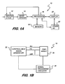
- FIG. 1A shows a digital camera 10 in an illustrative embodiment of the invention.
- the digital camera light from a subject scene is input to an imaging stage 12.
- the imaging stage may comprise conventional elements such as a lens, a neutral density filter, an iris and a shutter.
- the light is focused by the imaging stage 12 to form an image on an image sensor 14, which converts the incident light to electrical signals.
- the digital camera 10 further includes a processor 16, a memory 18, a display 20, and one or more additional input/output (I/O) elements 22.
- I/O input/output
- image sensor 14 is assumed in the present embodiment to be a CMOS image sensor, although other types of image sensors may be used in implementing the invention. As shown in FIG. 1B , image sensor 14 more particularly comprises a pixel array 30, a controllable signal generator 32 and signal processing circuitry 34. In other embodiments, one or both of elements 32 and 40 may be arranged external to the image sensor.
- the pixel array 30 generally comprises a plurality of pixels arranged in rows and columns.
- the pixel array may also incorporate at least a portion of the sampling and readout circuitry of the digital camera 10, as will be described below in conjunction with FIGS. 2, 3 , 5 and 8 .
- at least a portion of the sampling and readout circuitry may be formed integrally with the pixel array, for example, on a common integrated circuit with photodiodes and other elements of the pixel array.
- Elements 32 and 34 may also be viewed as part of the sampling and readout circuitry of the digital camera 10, and one or both of such elements may be formed integrally with the pixel array.
- Portions of the sampling and readout circuitry of the digital camera may also or alternatively be implemented in processor 16.
- sampling and readout circuitry as used herein is intended to be broadly construed so as to encompass any circuitry associated with the sampling and readout functionality of the digital camera 10, and portions of such circuitry may be arranged within image sensor 14 or elsewhere in the camera.
- a given readout process as described herein will typically incorporate sampling operations, and thus the circuitry that implements such a process is referred to as “sampling and readout circuitry.” This term should not be construed as requiring separate sampling and readout processes, or separate sampling circuitry and readout circuitry.
- the image sensor 14 will typically be implemented as a color image sensor having an associated CFA pattern.
- CFA patterns that may be used with the image sensor 14 include those described in the above-cited U.S. Patent Application Publication No. 2007/0024931 , although other CFA patterns may be used in other embodiments of the invention.
- the controllable signal generator 32 may operate under control of the processor 16 to generate signals associated with sampling and readout of the pixel array 30, including, by way of example, reset gate (RG), transfer gate (TG) and pixel power (VPP) signals. Other types of signals used to select particular rows and columns of the pixel array for processing may be generated by the signal generator 32.
- reset gate RG
- transfer gate TG
- VPP pixel power
- the signal processing circuitry 34 may comprise, for example, an analog signal processor for processing analog signals read out from the pixel array 30 and an analog-to-digital converter for converting such signals to a digital form suitable for processing by processor 16.
- the processor 16 may comprise, for example, a microprocessor, a central processing unit (CPU), an application-specific integrated circuit (ASIC), a digital signal processor (DSP), or other processing device, or combinations of multiple such devices.
- Various elements of the imaging stage 12 and the image sensor 14 may be controlled by timing signals or other signals supplied from the processor 16.
- the memory 18 may comprise any type of memory, such as, for example, random access memory (RAM), read-only memory (ROM), Flash memory, disk-based memory, or other types of storage elements, in any combination.
- RAM random access memory
- ROM read-only memory
- Flash memory disk-based memory
- Sampling and readout techniques as described herein may be implemented at least in part in the form of software that is stored in memory 18 and executed by processor 16.
- a given image captured by the image sensor 14 may be stored by the processor 16 in memory 18 and presented on display 20.
- the display 20 is typically an active matrix color liquid crystal display (LCD), although other types of displays may be used.
- the additional I/O elements 22 may comprise, for example, various on-screen controls, buttons or other user interfaces, network interfaces, memory card interfaces, etc.
- the digital camera as shown in FIG. 1A may comprise additional or alternative elements of a type known to those skilled in the art. Elements not specifically shown or described herein may be selected from those known in the art. As noted previously, the present invention may be implemented in a wide variety of other types of digital cameras or image capture devices. Also, as mentioned above, certain aspects of the embodiments described herein may be implemented at least in part in the form of software executed by one or more processing elements of an image capture device. Such software can be implemented in a straightforward manner given the teachings provided herein, as will be appreciated by those skilled in the art.
- the image sensor 14 as shown in FIG. 1B may be fabricated on a silicon substrate or other type of substrate.
- each pixel of the pixel array includes a photodiode and associated circuitry for measuring the light level at that pixel.
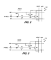
- FIG. 2 shows an illustrative embodiment of the circuitry associated with a given pixel 100 in the pixel array 30 of image sensor 14 of FIG. 1B .
- the pixel in this embodiment is assumed to be formed in an n-well on a p-type substrate of the image sensor.
- the pixel 100 comprises a photodiode 102 and three associated PMOS transistors P1, P2 and P3.
- the first transistor P1 transfers collected charge from the photodiode to a floating diffusion (FD) responsive to a transfer gate (TG) signal.
- TG transfer gate
- the transistor P1 itself is also commonly referred to as a transfer gate.
- the second transistor P2 is an output transistor configured to amplify the signal on the floating diffusion and to supply the amplified signal to an output voltage column line VOut.
- the third transistor P3 resets the floating diffusion by coupling it to a pixel power supply voltage VPP responsive to a reset gate (RG) signal.
- RG reset gate
- each pixel need not include its own reset transistor and output transistor as in the FIG. 2 arrangement.
- a given reset transistor and a given output transistor are shared among multiple pixels.
- An example of such a sharing arrangement will be described below in conjunction with FIG. 8 .
- the term "pixel" as used herein is intended to encompass, for example, a grouping of circuitry elements such as 102, P1, P2 and P3, or an alternative grouping comprising just 102 and P1 in an embodiment where pixel 100 shares P2 and P3 with other pixels. Numerous alternative arrangements of pixel circuitry may be used in these and other embodiments of the invention.
- the element R in FIG. 2 denotes the resistance of the n-well between the pixel 100 and the nearest n-well contact.
- the well bias voltage is typically introduced through well contacts in a ring around the periphery of the pixel array. These well contacts are close to edge pixels of the array but far from central pixels of the array, and thus the value of R for a pixel near the center of the array can be very large, leading to well bounce issues that are addressed in a manner to be described in greater detail below.
- At least a portion of the pixel circuitry of FIG. 2 may be repeated for each of the other pixels of the array 30. Pixels in the same row of the array share a common RG signal, while pixels in the same column of the array share the output voltage column line VOut. As indicated previously, the output transistor P2 and reset transistor P3 of the pixel circuitry may be shared between multiple pixels.
- FIG. 3 shows an NMOS equivalent of the PMOS pixel 100 described in conjunction with FIG. 2 .
- NMOS pixel 110 comprises photodiode 112 and NMOS transistors N1, N2 and N3. These elements are assumed to be formed in a p-well on an n-type substrate of the image sensor 14. The operation of the NMOS pixel 110 is analogous to that described previously for the PMOS pixel 100.
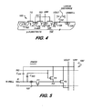
- FIG. 4 shows a cross-sectional view of the PMOS pixel 100 of FIG. 2 . It can be seen that the photodiode 102 and the three PMOS transistors are formed in an n-well 120 on a p-type substrate 122. The transistors P1, P2 and P3 are formed utilizing p+ diffusion regions 124, 126 and 128 as indicated. VNwell denotes a bias voltage applied to the n-well 120 via an n+ contact 130. As mentioned above, there may be a large distance between the bias voltage contact and the circuitry of the pixel 100, as illustrated by arrow 132 in FIG. 4 . This large resistance, represented by R in FIG. 2 , can make the n-well voltage unstable, leading to the well bounce problem previously described.
- FIG. 5 shows a PMOS pixel 100' that is similar to the PMOS pixel 100 of FIGS. 2 and 4 but includes capacitances that may be adjusted in accordance with an illustrative embodiment of the invention.
- the capacitance C PP represents the capacitance between the VPP signal line and the n-well 120.
- the capacitance C PP may more specifically indicate, for example, the capacitance between the p+ diffusion region 126, associated with reset transistor P3 and output transistor P2, and the well.
- the capacitance C RG represents the capacitance between the gate terminal of the reset transistor P3 and the n-well 120.
- FIG. 6 illustrates an exemplary row readout process for a pixel array 30 constructed using PMOS pixels 100' configured as shown in FIG. 5 .
- the RG signals for the respective rows of the pixel array are all in an active state. This connects all floating diffusions to the VPP line which is in an inactive state. Thus, all output transistors P2 are in an inactive state because their inputs are inactive.
- active state and “inactive state” will be used herein to refer to the binary logic states of a given signal, signal line, transistor or floating diffusion.
- the active and inactive states of a transistor may be viewed as generally corresponding to “on” and “off' states, respectively.
- PMOS transistors such as P1, P2 and P3
- logic low input signals will turn these devices on, and logic high input signals will turn these devices off.
- the active states of the TG, RG and VPP signals and their associated signal lines in the PMOS pixel circuitry of FIG. 5 correspond to low voltages
- the inactive states of these signals and associated signal lines correspond to higher voltages.
- the higher voltage level associated with an inactive state of a given signal or signal line is typically slightly less than the bias voltage of the n-well in order to prevent charge leakage from the floating diffusion over the transfer gate P1 and into the photodiode 102.
- the n-well bias voltage is 2.7 volts
- a given inactive state voltage level may be on the order of about 2.2 volts.
- all RG signals other than that of the given row are switched to an inactive state at time T1.
- the VPP voltage is switched to an active state at time T2. Since the RG signal of the selected row is still active, all floating diffusions and output transistors of that row also switch to their active states. The floating diffusions and output transistors of all other rows remain in their inactive states.
- RG signals other than that of the selected row it is desirable for all RG signals other than that of the selected row to transition from active to inactive prior to the VPP signal transitioning from inactive to active. This ensures that all of the floating diffusions in the non-selected rows remain in their inactive states, which advantageously tends to reduce well bounce.
- at least one of the RG signals other than that of the selected row transitions from its active state to its inactive state within a predetermined time prior to the transition of the VPP line from its inactive state to its active state.
- This predetermined time prior to the transition of the VPP line from its inactive state to its active state is preferably less than or equal to approximately 500 nanoseconds (ns). For example, a value on the order of 200 ns may be used in a given embodiment.
- the RG signal of the selected row is then switched to the inactive state at time T3 and the output voltage column line VOut is sampled to obtain a first output voltage level 150.
- the TG signal of the selected row is pulsed from inactive to active and back to inactive. This transfers charge from the photodiodes of that row to their respective floating diffusions.
- the duration of the pulse is from time T4 to time T5.
- the output voltage column line VOut is then sampled again to obtain a second voltage level 160.
- the difference between the first and second voltage levels 150 and 160 provides a measure of the charge magnitude for the corresponding photodiode. This difference may be determined, for example, in other circuitry associated with the image sensor 14, such as the signal processing circuitry 34, or in another element of the digital camera of FIG. 1A , such as processor 16.
- the charge magnitudes for the other photodiodes in the selected row are determined in a similar manner.
- the VPP voltage is switched back to the inactive state at time T6, and then all of the RG signals are switched to the active state at time T7. It is desirable for the VPP signal to transition from active to inactive prior to the RG signals transitioning from inactive to active. This prevents the floating diffusions of the non-selected rows from changing voltage, again tending to reduce well bounce.
- at least one of the RG signals other than that of the selected row transitions from its inactive state to its active state within a predetermined time after the transition of the VPP line from its active state to its inactive state.
- This predetermined time after the transition of the VPP line from its active state to its inactive state is preferably less than or equal to approximately 500 ns. Again, a value on the order of 200 ns may be used in a given embodiment, as one particular example, although other values could be used.
- the RG signals of all rows other than the selected row transition from an active state to an inactive state. This turns off the reset transistors P3 in all rows other than the selected row.
- the amount of charge in the n-well that is displaced by turning off the reset transistor P3 of a given pixel 100' in a non-selected row may be estimated as C RG ⁇ V RG , where ⁇ V RG is the change in voltage level of the RG signal as indicated in FIG. 6 .
- the amount of charge in the n-well that is displaced by transitioning the VPP signal for that pixel from its inactive state to its active state at time T2 may be estimated as C PP ⁇ V PP , where ⁇ V PP is the change in voltage level of the VPP signal as indicated in FIG. 6 . If T2 and T1 are separated by a sufficiently small time period, such as 500 ns or less as noted above, then the two charge displacements will substantially cancel each other out: C RG ⁇ ⁇ ⁇ V RG + C PP ⁇ ⁇ ⁇ V PP ⁇ 0. This equation is an example of what is more generally referred to herein as a charge balancing equation.
- a similar charge balancing can be achieved if times T6 and T7 are separated by a sufficiently small time period, again about 500 ns or less as previously indicated.
- the VPP signal transitions from its active state to its inactive state at time T6, followed at time T7 by the RG signals of all of the rows of the array transitioning from inactive to active states.
- transitioning RG and VPP with opposite polarities at nearly the same time cancels out the charge displacements on the n-well caused by the capacitances C PP and C RG .
- the charge balancing equation can be satisfied by adjusting one or more of the capacitances C PP and C RG or one or more of the voltage level changes ⁇ V RG and ⁇ V PP , in any combination.
- an embodiment of the invention may configure the image sensor 14 such that the values of the capacitances C PP and C RG of the pixels are adjusted based on given values of voltage level changes ⁇ V RG and ⁇ V PP so as to satisfy the charge balance equation.
- the capacitance C PP can be adjusted, for example, by changing the size of the source diffusion regions associated with the reset or output transistors.
- the capacitance C RG can be adjusted, for example, by changing the area of the reset transistor gate terminal or by connecting the reset transistor to an additional p+ diffusion region.
- the capacitances C PP and C RG may be given, for example, based on known parasitic capacitance values within the image sensor, and one or both of the voltage level changes ⁇ V RG and ⁇ V PP may be adjusted so as to satisfy the charge balance equation. Adjustments in the voltage level changes can be achieved, for example, by appropriate controlled generation of RG and VPP signals in controllable signal generator 32 or other signal generation circuitry associated with or incorporated in the image sensor 14. For example, a number of different selectable signal levels may be provided, with the selection of particular levels for use in a given image sensor being based on detected levels of well bounce.
- a given such adjustment in capacitances or voltage level changes may be made uniformly throughout the pixel array. It is also possible that such adjustments may be made only for certain portions of the array, such as central portions that are more susceptible to the well bounce problem.
- the above-noted exemplary charge balancing equation may alternatively be expressed as follows: C RG ⁇ ⁇ ⁇ V RG ⁇ C PP ⁇ ⁇ ⁇ V PP , with the approximation being met if the two magnitudes
- Other charge balancing equations specifying estimated charge displacements in the well associated with the relevant transitions in the RG and VPP signals may be used in alternative embodiments to provide the desired reduction in well bounce.
- FIG. 7 shows a timing diagram that is generally the same as FIG. 6 but for an embodiment with NMOS pixels. It can be seen that the voltage levels in the FIG. 7 timing diagram are complementary to those of the FIG. 6 diagram, but the signal transition timing and basic operation are otherwise the same.
- FIG. 8 shows a version of the NMOS pixel circuitry configured with sharing of an output transistor N2' and a reset transistor N3' by a group of four pixels.
- the four pixels include respective photodiodes 812-0, 812-1, 812-2 and 812-3 coupled to respective transfer gates N1-0, N1-1, N1-2 and N1-3 as shown.
- the resistance R' in this embodiment represents the resistance of the p-well in which the photodiodes and the NMOS transistors are formed.
- An analogous set of PMOS circuitry may be formed in a complementary manner.
- numerous alternative arrangements for sharing of output transistors, reset transistors, floating diffusions or other types of pixel circuitry among multiple pixels may be used. For example, more or fewer than four pixels may be part of a given group configured to share pixel circuitry.
- the image sensor 14 may include additional sampling and readout circuitry, such as, for example, otherwise conventional column circuitry and row circuitry commonly utilized in sampling and readout of pixel array. Such additional circuitry, being well understood by those skilled in the art, is not described in detail herein.
Landscapes
- Engineering & Computer Science (AREA)
- Multimedia (AREA)
- Signal Processing (AREA)
- Transforming Light Signals Into Electric Signals (AREA)
- Solid State Image Pick-Up Elements (AREA)
Applications Claiming Priority (2)
| Application Number | Priority Date | Filing Date | Title |
|---|---|---|---|
| US12/129,999 US7807955B2 (en) | 2008-05-30 | 2008-05-30 | Image sensor having reduced well bounce |
| PCT/US2009/002921 WO2009145867A1 (en) | 2008-05-30 | 2009-05-12 | Image sensor having reduced well bounce |
Publications (2)
| Publication Number | Publication Date |
|---|---|
| EP2286579A1 EP2286579A1 (en) | 2011-02-23 |
| EP2286579B1 true EP2286579B1 (en) | 2013-07-10 |
Family
ID=41040892
Family Applications (1)
| Application Number | Title | Priority Date | Filing Date |
|---|---|---|---|
| EP09755230.1A Active EP2286579B1 (en) | 2008-05-30 | 2009-05-12 | Image sensor having reduced well bounce |
Country Status (7)
| Country | Link |
|---|---|
| US (1) | US7807955B2 (enExample) |
| EP (1) | EP2286579B1 (enExample) |
| JP (1) | JP5520937B2 (enExample) |
| KR (1) | KR101460585B1 (enExample) |
| CN (1) | CN102037723B (enExample) |
| TW (1) | TWI514873B (enExample) |
| WO (1) | WO2009145867A1 (enExample) |
Families Citing this family (11)
| Publication number | Priority date | Publication date | Assignee | Title |
|---|---|---|---|---|
| US8139130B2 (en) | 2005-07-28 | 2012-03-20 | Omnivision Technologies, Inc. | Image sensor with improved light sensitivity |
| US8274715B2 (en) | 2005-07-28 | 2012-09-25 | Omnivision Technologies, Inc. | Processing color and panchromatic pixels |
| US7916362B2 (en) | 2006-05-22 | 2011-03-29 | Eastman Kodak Company | Image sensor with improved light sensitivity |
| US8031258B2 (en) | 2006-10-04 | 2011-10-04 | Omnivision Technologies, Inc. | Providing multiple video signals from single sensor |
| JP6132500B2 (ja) * | 2012-09-24 | 2017-05-24 | キヤノン株式会社 | 撮像装置、撮像装置の駆動方法、および撮像システム。 |
| US9344658B2 (en) * | 2014-07-31 | 2016-05-17 | Omnivision Technologies, Inc. | Negative biased substrate for pixels in stacked image sensors |
| KR102612194B1 (ko) * | 2016-12-14 | 2023-12-11 | 삼성전자주식회사 | 이벤트 기반 센서 및 이벤트 기반 센싱 방법 |
| CN113632453B (zh) * | 2019-03-27 | 2025-04-04 | 苹果公司 | 具有多个功率状态的传感器架构的硬件实现方式 |
| WO2020197956A1 (en) * | 2019-03-27 | 2020-10-01 | Ocelot Laboratories Llc | Sensor system architecture with feedback loop and multiple power states |
| CN114339084B (zh) * | 2020-09-30 | 2025-04-25 | 思特威(上海)电子科技股份有限公司 | Tof图像传感器像素结构及测距系统 |
| US12250099B2 (en) * | 2021-09-08 | 2025-03-11 | PassiveLogic, Inc. | External activation of quiescent device |
Family Cites Families (18)
| Publication number | Priority date | Publication date | Assignee | Title |
|---|---|---|---|---|
| JPH0775633A (ja) * | 1993-06-30 | 1995-03-20 | Shimadzu Corp | 画像処理装置 |
| US6115066A (en) * | 1997-06-12 | 2000-09-05 | International Business Machines Corporation | Image sensor with direct digital correlated sampling |
| JPH1126741A (ja) * | 1997-07-04 | 1999-01-29 | Toshiba Corp | 固体撮像装置 |
| US6369853B1 (en) * | 1997-11-13 | 2002-04-09 | Foveon, Inc. | Intra-pixel frame storage element, array, and electronic shutter method suitable for electronic still camera applications |
| US6727521B2 (en) * | 2000-09-25 | 2004-04-27 | Foveon, Inc. | Vertical color filter detector group and array |
| JP3467013B2 (ja) * | 1999-12-06 | 2003-11-17 | キヤノン株式会社 | 固体撮像装置 |
| US6995795B1 (en) * | 2000-09-12 | 2006-02-07 | Eastman Kodak Company | Method for reducing dark current |
| US6586784B1 (en) | 2002-10-02 | 2003-07-01 | Eastman Kodak Company | Accumulation mode clocking of a charge-coupled device |
| JP4120453B2 (ja) * | 2003-04-18 | 2008-07-16 | ソニー株式会社 | 固体撮像装置とその駆動制御方法 |
| JP4207659B2 (ja) * | 2003-05-16 | 2009-01-14 | ソニー株式会社 | 固体撮像装置およびその駆動方法、ならびにカメラ装置 |
| JP4075773B2 (ja) * | 2003-11-05 | 2008-04-16 | ソニー株式会社 | 固体撮像装置 |
| US7075129B2 (en) * | 2004-01-09 | 2006-07-11 | Eastman Kodak Company | Image sensor with reduced p-well conductivity |
| JP4424120B2 (ja) * | 2004-08-31 | 2010-03-03 | ソニー株式会社 | 固体撮像装置および固体撮像装置の製造方法 |
| JP4916101B2 (ja) * | 2004-09-01 | 2012-04-11 | キヤノン株式会社 | 光電変換装置、固体撮像装置及び固体撮像システム |
| JP4756839B2 (ja) * | 2004-09-01 | 2011-08-24 | キヤノン株式会社 | 固体撮像装置及びカメラ |
| KR100660865B1 (ko) * | 2005-06-08 | 2006-12-26 | 삼성전자주식회사 | 이미지 센서에서 공유된 배선/트랜지스터를 가지는 픽셀회로 및 구동 방법 |
| US8139130B2 (en) * | 2005-07-28 | 2012-03-20 | Omnivision Technologies, Inc. | Image sensor with improved light sensitivity |
| JP2007095917A (ja) * | 2005-09-28 | 2007-04-12 | Matsushita Electric Ind Co Ltd | 固体撮像装置 |
-
2008
- 2008-05-30 US US12/129,999 patent/US7807955B2/en active Active
-
2009
- 2009-05-12 CN CN200980118679.1A patent/CN102037723B/zh active Active
- 2009-05-12 KR KR1020107029758A patent/KR101460585B1/ko active Active
- 2009-05-12 EP EP09755230.1A patent/EP2286579B1/en active Active
- 2009-05-12 WO PCT/US2009/002921 patent/WO2009145867A1/en not_active Ceased
- 2009-05-12 JP JP2011511595A patent/JP5520937B2/ja active Active
- 2009-05-27 TW TW098117886A patent/TWI514873B/zh active
Also Published As
| Publication number | Publication date |
|---|---|
| WO2009145867A1 (en) | 2009-12-03 |
| JP5520937B2 (ja) | 2014-06-11 |
| US7807955B2 (en) | 2010-10-05 |
| US20090294631A1 (en) | 2009-12-03 |
| KR101460585B1 (ko) | 2014-11-13 |
| CN102037723A (zh) | 2011-04-27 |
| JP2011522483A (ja) | 2011-07-28 |
| TWI514873B (zh) | 2015-12-21 |
| EP2286579A1 (en) | 2011-02-23 |
| TW201004331A (en) | 2010-01-16 |
| CN102037723B (zh) | 2014-06-04 |
| KR20110025673A (ko) | 2011-03-10 |
Similar Documents
| Publication | Publication Date | Title |
|---|---|---|
| EP2286579B1 (en) | Image sensor having reduced well bounce | |
| US20230097274A1 (en) | Imaging device including photoelectric converters and capacitive element | |
| US8174601B2 (en) | Image sensor with controllable transfer gate off state voltage levels | |
| EP1515540B1 (en) | Semiconductor device, and control method and device for driving unit component of semiconductor device | |
| JP5154908B2 (ja) | Cmosイメージセンサのための、小サイズ、高利得及び低ノイズのピクセル | |
| US7427790B2 (en) | Image sensor with gain control | |
| US12266672B2 (en) | Image sensing device | |
| US11652117B2 (en) | Image sensing device | |
| CN212572732U (zh) | 图像传感器和放大电路 | |
| US20110267516A1 (en) | Electronic shutter control in image sensors | |
| US20110267517A1 (en) | Electronic shutter control in image sensors | |
| CN114143483B (zh) | 图像感测装置 | |
| US8106427B2 (en) | Image sensor with well bounce correction | |
| US8648950B2 (en) | Image sensor for minimizing variation of control signal level | |
| US8184186B2 (en) | Electronic shutter control in image sensors | |
| CN112135072A (zh) | 图像传感器 | |
| JP2004048813A (ja) | 固体撮像装置 | |
| JP4561651B2 (ja) | 固体撮像素子 | |
| JP2001119628A (ja) | 固体撮像素子 |
Legal Events
| Date | Code | Title | Description |
|---|---|---|---|
| PUAI | Public reference made under article 153(3) epc to a published international application that has entered the european phase |
Free format text: ORIGINAL CODE: 0009012 |
|
| 17P | Request for examination filed |
Effective date: 20101201 |
|
| AK | Designated contracting states |
Kind code of ref document: A1 Designated state(s): AT BE BG CH CY CZ DE DK EE ES FI FR GB GR HR HU IE IS IT LI LT LU LV MC MK MT NL NO PL PT RO SE SI SK TR |
|
| AX | Request for extension of the european patent |
Extension state: AL BA RS |
|
| DAX | Request for extension of the european patent (deleted) | ||
| RAP1 | Party data changed (applicant data changed or rights of an application transferred) |
Owner name: OMNIVISION TECHNOLOGIES, INC. |
|
| 17Q | First examination report despatched |
Effective date: 20120316 |
|
| REG | Reference to a national code |
Ref country code: DE Ref legal event code: R079 Ref document number: 602009017068 Country of ref document: DE Free format text: PREVIOUS MAIN CLASS: H04N0003150000 Ipc: H04N0005365000 |
|
| RIC1 | Information provided on ipc code assigned before grant |
Ipc: H04N 5/3745 20110101ALI20121029BHEP Ipc: H04N 5/365 20110101AFI20121029BHEP |
|
| GRAP | Despatch of communication of intention to grant a patent |
Free format text: ORIGINAL CODE: EPIDOSNIGR1 |
|
| GRAS | Grant fee paid |
Free format text: ORIGINAL CODE: EPIDOSNIGR3 |
|
| GRAA | (expected) grant |
Free format text: ORIGINAL CODE: 0009210 |
|
| AK | Designated contracting states |
Kind code of ref document: B1 Designated state(s): AT BE BG CH CY CZ DE DK EE ES FI FR GB GR HR HU IE IS IT LI LT LU LV MC MK MT NL NO PL PT RO SE SI SK TR |
|
| REG | Reference to a national code |
Ref country code: GB Ref legal event code: FG4D |
|
| REG | Reference to a national code |
Ref country code: AT Ref legal event code: REF Ref document number: 621519 Country of ref document: AT Kind code of ref document: T Effective date: 20130715 Ref country code: CH Ref legal event code: EP |
|
| REG | Reference to a national code |
Ref country code: IE Ref legal event code: FG4D |
|
| REG | Reference to a national code |
Ref country code: DE Ref legal event code: R096 Ref document number: 602009017068 Country of ref document: DE Effective date: 20130905 |
|
| PG25 | Lapsed in a contracting state [announced via postgrant information from national office to epo] |
Ref country code: SI Free format text: LAPSE BECAUSE OF FAILURE TO SUBMIT A TRANSLATION OF THE DESCRIPTION OR TO PAY THE FEE WITHIN THE PRESCRIBED TIME-LIMIT Effective date: 20130710 |
|
| REG | Reference to a national code |
Ref country code: AT Ref legal event code: MK05 Ref document number: 621519 Country of ref document: AT Kind code of ref document: T Effective date: 20130710 |
|
| REG | Reference to a national code |
Ref country code: NL Ref legal event code: VDEP Effective date: 20130710 |
|
| REG | Reference to a national code |
Ref country code: LT Ref legal event code: MG4D |
|
| PG25 | Lapsed in a contracting state [announced via postgrant information from national office to epo] |
Ref country code: PT Free format text: LAPSE BECAUSE OF FAILURE TO SUBMIT A TRANSLATION OF THE DESCRIPTION OR TO PAY THE FEE WITHIN THE PRESCRIBED TIME-LIMIT Effective date: 20131111 Ref country code: CY Free format text: LAPSE BECAUSE OF FAILURE TO SUBMIT A TRANSLATION OF THE DESCRIPTION OR TO PAY THE FEE WITHIN THE PRESCRIBED TIME-LIMIT Effective date: 20130918 Ref country code: NO Free format text: LAPSE BECAUSE OF FAILURE TO SUBMIT A TRANSLATION OF THE DESCRIPTION OR TO PAY THE FEE WITHIN THE PRESCRIBED TIME-LIMIT Effective date: 20131010 Ref country code: AT Free format text: LAPSE BECAUSE OF FAILURE TO SUBMIT A TRANSLATION OF THE DESCRIPTION OR TO PAY THE FEE WITHIN THE PRESCRIBED TIME-LIMIT Effective date: 20130710 Ref country code: LT Free format text: LAPSE BECAUSE OF FAILURE TO SUBMIT A TRANSLATION OF THE DESCRIPTION OR TO PAY THE FEE WITHIN THE PRESCRIBED TIME-LIMIT Effective date: 20130710 Ref country code: HR Free format text: LAPSE BECAUSE OF FAILURE TO SUBMIT A TRANSLATION OF THE DESCRIPTION OR TO PAY THE FEE WITHIN THE PRESCRIBED TIME-LIMIT Effective date: 20130710 Ref country code: IS Free format text: LAPSE BECAUSE OF FAILURE TO SUBMIT A TRANSLATION OF THE DESCRIPTION OR TO PAY THE FEE WITHIN THE PRESCRIBED TIME-LIMIT Effective date: 20131110 Ref country code: BE Free format text: LAPSE BECAUSE OF FAILURE TO SUBMIT A TRANSLATION OF THE DESCRIPTION OR TO PAY THE FEE WITHIN THE PRESCRIBED TIME-LIMIT Effective date: 20130710 Ref country code: SE Free format text: LAPSE BECAUSE OF FAILURE TO SUBMIT A TRANSLATION OF THE DESCRIPTION OR TO PAY THE FEE WITHIN THE PRESCRIBED TIME-LIMIT Effective date: 20130710 |
|
| PG25 | Lapsed in a contracting state [announced via postgrant information from national office to epo] |
Ref country code: LV Free format text: LAPSE BECAUSE OF FAILURE TO SUBMIT A TRANSLATION OF THE DESCRIPTION OR TO PAY THE FEE WITHIN THE PRESCRIBED TIME-LIMIT Effective date: 20130710 Ref country code: NL Free format text: LAPSE BECAUSE OF FAILURE TO SUBMIT A TRANSLATION OF THE DESCRIPTION OR TO PAY THE FEE WITHIN THE PRESCRIBED TIME-LIMIT Effective date: 20130710 Ref country code: ES Free format text: LAPSE BECAUSE OF FAILURE TO SUBMIT A TRANSLATION OF THE DESCRIPTION OR TO PAY THE FEE WITHIN THE PRESCRIBED TIME-LIMIT Effective date: 20131021 Ref country code: GR Free format text: LAPSE BECAUSE OF FAILURE TO SUBMIT A TRANSLATION OF THE DESCRIPTION OR TO PAY THE FEE WITHIN THE PRESCRIBED TIME-LIMIT Effective date: 20131011 Ref country code: PL Free format text: LAPSE BECAUSE OF FAILURE TO SUBMIT A TRANSLATION OF THE DESCRIPTION OR TO PAY THE FEE WITHIN THE PRESCRIBED TIME-LIMIT Effective date: 20130710 Ref country code: FI Free format text: LAPSE BECAUSE OF FAILURE TO SUBMIT A TRANSLATION OF THE DESCRIPTION OR TO PAY THE FEE WITHIN THE PRESCRIBED TIME-LIMIT Effective date: 20130710 |
|
| PG25 | Lapsed in a contracting state [announced via postgrant information from national office to epo] |
Ref country code: CY Free format text: LAPSE BECAUSE OF FAILURE TO SUBMIT A TRANSLATION OF THE DESCRIPTION OR TO PAY THE FEE WITHIN THE PRESCRIBED TIME-LIMIT Effective date: 20130710 |
|
| PG25 | Lapsed in a contracting state [announced via postgrant information from national office to epo] |
Ref country code: CZ Free format text: LAPSE BECAUSE OF FAILURE TO SUBMIT A TRANSLATION OF THE DESCRIPTION OR TO PAY THE FEE WITHIN THE PRESCRIBED TIME-LIMIT Effective date: 20130710 Ref country code: DK Free format text: LAPSE BECAUSE OF FAILURE TO SUBMIT A TRANSLATION OF THE DESCRIPTION OR TO PAY THE FEE WITHIN THE PRESCRIBED TIME-LIMIT Effective date: 20130710 Ref country code: SK Free format text: LAPSE BECAUSE OF FAILURE TO SUBMIT A TRANSLATION OF THE DESCRIPTION OR TO PAY THE FEE WITHIN THE PRESCRIBED TIME-LIMIT Effective date: 20130710 Ref country code: EE Free format text: LAPSE BECAUSE OF FAILURE TO SUBMIT A TRANSLATION OF THE DESCRIPTION OR TO PAY THE FEE WITHIN THE PRESCRIBED TIME-LIMIT Effective date: 20130710 Ref country code: RO Free format text: LAPSE BECAUSE OF FAILURE TO SUBMIT A TRANSLATION OF THE DESCRIPTION OR TO PAY THE FEE WITHIN THE PRESCRIBED TIME-LIMIT Effective date: 20130710 |
|
| PLBE | No opposition filed within time limit |
Free format text: ORIGINAL CODE: 0009261 |
|
| STAA | Information on the status of an ep patent application or granted ep patent |
Free format text: STATUS: NO OPPOSITION FILED WITHIN TIME LIMIT |
|
| PG25 | Lapsed in a contracting state [announced via postgrant information from national office to epo] |
Ref country code: IT Free format text: LAPSE BECAUSE OF FAILURE TO SUBMIT A TRANSLATION OF THE DESCRIPTION OR TO PAY THE FEE WITHIN THE PRESCRIBED TIME-LIMIT Effective date: 20130710 |
|
| 26N | No opposition filed |
Effective date: 20140411 |
|
| REG | Reference to a national code |
Ref country code: DE Ref legal event code: R097 Ref document number: 602009017068 Country of ref document: DE Effective date: 20140411 |
|
| PG25 | Lapsed in a contracting state [announced via postgrant information from national office to epo] |
Ref country code: LU Free format text: LAPSE BECAUSE OF FAILURE TO SUBMIT A TRANSLATION OF THE DESCRIPTION OR TO PAY THE FEE WITHIN THE PRESCRIBED TIME-LIMIT Effective date: 20140512 |
|
| PG25 | Lapsed in a contracting state [announced via postgrant information from national office to epo] |
Ref country code: MC Free format text: LAPSE BECAUSE OF FAILURE TO SUBMIT A TRANSLATION OF THE DESCRIPTION OR TO PAY THE FEE WITHIN THE PRESCRIBED TIME-LIMIT Effective date: 20130710 |
|
| REG | Reference to a national code |
Ref country code: IE Ref legal event code: MM4A |
|
| PG25 | Lapsed in a contracting state [announced via postgrant information from national office to epo] |
Ref country code: IE Free format text: LAPSE BECAUSE OF NON-PAYMENT OF DUE FEES Effective date: 20140512 |
|
| PG25 | Lapsed in a contracting state [announced via postgrant information from national office to epo] |
Ref country code: MT Free format text: LAPSE BECAUSE OF FAILURE TO SUBMIT A TRANSLATION OF THE DESCRIPTION OR TO PAY THE FEE WITHIN THE PRESCRIBED TIME-LIMIT Effective date: 20130710 |
|
| REG | Reference to a national code |
Ref country code: FR Ref legal event code: PLFP Year of fee payment: 8 |
|
| PG25 | Lapsed in a contracting state [announced via postgrant information from national office to epo] |
Ref country code: BG Free format text: LAPSE BECAUSE OF FAILURE TO SUBMIT A TRANSLATION OF THE DESCRIPTION OR TO PAY THE FEE WITHIN THE PRESCRIBED TIME-LIMIT Effective date: 20130710 |
|
| PG25 | Lapsed in a contracting state [announced via postgrant information from national office to epo] |
Ref country code: TR Free format text: LAPSE BECAUSE OF FAILURE TO SUBMIT A TRANSLATION OF THE DESCRIPTION OR TO PAY THE FEE WITHIN THE PRESCRIBED TIME-LIMIT Effective date: 20130710 Ref country code: HU Free format text: LAPSE BECAUSE OF FAILURE TO SUBMIT A TRANSLATION OF THE DESCRIPTION OR TO PAY THE FEE WITHIN THE PRESCRIBED TIME-LIMIT; INVALID AB INITIO Effective date: 20090512 |
|
| REG | Reference to a national code |
Ref country code: FR Ref legal event code: PLFP Year of fee payment: 9 |
|
| REG | Reference to a national code |
Ref country code: FR Ref legal event code: PLFP Year of fee payment: 10 |
|
| PG25 | Lapsed in a contracting state [announced via postgrant information from national office to epo] |
Ref country code: MK Free format text: LAPSE BECAUSE OF FAILURE TO SUBMIT A TRANSLATION OF THE DESCRIPTION OR TO PAY THE FEE WITHIN THE PRESCRIBED TIME-LIMIT Effective date: 20130710 |
|
| REG | Reference to a national code |
Ref country code: DE Ref legal event code: R079 Ref document number: 602009017068 Country of ref document: DE Free format text: PREVIOUS MAIN CLASS: H04N0005365000 Ipc: H04N0025670000 |
|
| REG | Reference to a national code |
Ref country code: FR Ref legal event code: PLFP Year of fee payment: 15 |
|
| P01 | Opt-out of the competence of the unified patent court (upc) registered |
Effective date: 20230419 |
|
| PGFP | Annual fee paid to national office [announced via postgrant information from national office to epo] |
Ref country code: DE Payment date: 20250409 Year of fee payment: 17 |
|
| PGFP | Annual fee paid to national office [announced via postgrant information from national office to epo] |
Ref country code: GB Payment date: 20250410 Year of fee payment: 17 |
|
| PGFP | Annual fee paid to national office [announced via postgrant information from national office to epo] |
Ref country code: FR Payment date: 20250409 Year of fee payment: 17 |
|
| PGFP | Annual fee paid to national office [announced via postgrant information from national office to epo] |
Ref country code: CH Payment date: 20250601 Year of fee payment: 17 |