EP2277262B1 - Vorwärtskopplungslinearisierung von hf-leistungsverstärkern - Google Patents
Vorwärtskopplungslinearisierung von hf-leistungsverstärkern Download PDFInfo
- Publication number
- EP2277262B1 EP2277262B1 EP09726729.8A EP09726729A EP2277262B1 EP 2277262 B1 EP2277262 B1 EP 2277262B1 EP 09726729 A EP09726729 A EP 09726729A EP 2277262 B1 EP2277262 B1 EP 2277262B1
- Authority
- EP
- European Patent Office
- Prior art keywords
- signal
- amplifier
- analog
- digital
- digital data
- Prior art date
- Legal status (The legal status is an assumption and is not a legal conclusion. Google has not performed a legal analysis and makes no representation as to the accuracy of the status listed.)
- Not-in-force
Links
- 238000000034 method Methods 0.000 claims description 16
- 238000006243 chemical reaction Methods 0.000 claims description 6
- 238000012544 monitoring process Methods 0.000 claims 2
- 238000012545 processing Methods 0.000 description 7
- 238000013461 design Methods 0.000 description 5
- 230000008901 benefit Effects 0.000 description 4
- 238000010586 diagram Methods 0.000 description 4
- 230000006870 function Effects 0.000 description 4
- 230000005540 biological transmission Effects 0.000 description 3
- 238000004891 communication Methods 0.000 description 3
- 238000004590 computer program Methods 0.000 description 3
- 230000008878 coupling Effects 0.000 description 3
- 238000010168 coupling process Methods 0.000 description 3
- 238000005859 coupling reaction Methods 0.000 description 3
- 230000003111 delayed effect Effects 0.000 description 3
- 230000001419 dependent effect Effects 0.000 description 3
- 230000008030 elimination Effects 0.000 description 3
- 238000003379 elimination reaction Methods 0.000 description 3
- 230000008569 process Effects 0.000 description 3
- 230000003321 amplification Effects 0.000 description 2
- 238000013459 approach Methods 0.000 description 2
- 230000001934 delay Effects 0.000 description 2
- 238000003199 nucleic acid amplification method Methods 0.000 description 2
- 230000003595 spectral effect Effects 0.000 description 2
- 230000002411 adverse Effects 0.000 description 1
- 230000003466 anti-cipated effect Effects 0.000 description 1
- 238000004883 computer application Methods 0.000 description 1
- 238000010276 construction Methods 0.000 description 1
- 230000006872 improvement Effects 0.000 description 1
- 230000010365 information processing Effects 0.000 description 1
- 238000009434 installation Methods 0.000 description 1
- 239000000463 material Substances 0.000 description 1
- 238000013508 migration Methods 0.000 description 1
- 230000005012 migration Effects 0.000 description 1
- 238000012986 modification Methods 0.000 description 1
- 230000004048 modification Effects 0.000 description 1
- 238000012546 transfer Methods 0.000 description 1
- 239000013598 vector Substances 0.000 description 1
- 239000002918 waste heat Substances 0.000 description 1
Images
Classifications
-
- H—ELECTRICITY
- H03—ELECTRONIC CIRCUITRY
- H03F—AMPLIFIERS
- H03F1/00—Details of amplifiers with only discharge tubes, only semiconductor devices or only unspecified devices as amplifying elements
- H03F1/32—Modifications of amplifiers to reduce non-linear distortion
- H03F1/3223—Modifications of amplifiers to reduce non-linear distortion using feed-forward
- H03F1/3229—Modifications of amplifiers to reduce non-linear distortion using feed-forward using a loop for error extraction and another loop for error subtraction
Definitions
- the inventive arrangements relate to methods for linearizing RF power amplifiers, and more particularly to a method for providing an envelope elimination and restoration (EER) amplifier with enhanced linearity.
- EER envelope elimination and restoration
- United States Patent 7,034,614 discloses a modified polar amplifier incorporating a feedforward linearization and having a fixed delay in the amplification path.
- EER amplifiers are well known in the art and can achieve very highly efficient conversion of DC energy to RF energy for complex waveforms having a varying envelope. They operate by separately processing the envelope and phase information contained in a modulated input signal. The phase information is communicated to a power amplifier where it is amplified as a constant envelope signal. This permits such phase information to be amplified using highly efficient non-linear amplifiers. The envelope information contained in the input signal is restored to the phase information after the signal has been amplified.
- EER amplifiers using Class E topologies are known to have poor linearity.
- This poor linearity causes significant amounts of signal distortion.
- such distortion often arises from pulse-width modulator circuits that are used to control the output envelope voltage, and from switching non-linearities which exist in the circuit used for amplifying the phase information.
- the nonlinearities cause spectral re-growth (out-of-band noise), which leads to adjacent channel interference. It also causes in-band distortion, which degrades the bit-error rate (BER) performance for digital modulation waveforms.
- BER bit-error rate
- Distortion associated with RF power amplifiers is often characterized by means of an amplitude to amplitude (AM-to-AM) modulation curve and an amplitude-to-phase (AM-to-PM) modulation curve.
- the AM-to-AM modulation curve shows the RF power amplifier gain as a function of the input power.
- the AM-to-PM modulation curve shows the output phase variation of the RF power amplifier as a function of the input power.
- feedforward linearization One well known method for improving the linearity of RF power amplifiers is known as feedforward linearization.
- an RF splitter is typically used to separate a source signal into two separate signals. These two signals include a amplifier input signal and a reference signal.
- the amplifier input signal is provided to the amplifier as an input.
- a directional RF coupler is used to obtain a sample of the distorted output signal from the RF power amplifier.
- the reference signal and the sampled output from the directional coupler are communicated to separate inputs of a 180° hybrid RF signal combiner.
- the 180° hybrid RF hybrid combiner subtracts the reference signal from the distorted amplifier output.
- the resulting output from the combiner is an error signal.
- the error signal is subsequently amplified so as to scale the error signal to equal the power level of any distortion contained in the distorted output signal from the RF power amplifier.
- the error signal is then subtracted from the distorted output signal of the RF power amplifier to remove the distortion from the output signal.
- Feedforward linearization is effective at improving amplifier linearity.
- the relatively large magnitude of the error signal needed to improve the linearity of highly non-linear amplifiers can require a relatively high power RF amplifier for scaling the error signal.
- the necessity for such a relatively high power RF amplifier for scaling the error signal can reduce the overall efficiency of the amplifier system.
- feedforward linearization has been limited with regard to its usefulness as applied to highly non-linear amplifiers, such as the EER type amplifier.
- feedforward linearization Another limitation of feedforward linearization concerns bandwidth.
- the error signal In feedforward linearization systems, it is important for the error signal to be a highly accurate representation of the actual distortion produced by the RF power amplifier. A distorted error signal will not properly remove non-linearities from the output of the amplifier.
- the signals to be amplified are wideband RF signals inaccuracy of the error signal can occur. For example, such inaccuracies can result from amplitude and phase variations which exist across the operating bandwidth of the RF components used to form and process the error signal.
- RF components can include RF signal splitters and 180° RF hybrid combiner circuits.
- the invention concerns an RF amplifier system incorporating feedforward linearization.
- the system includes a digital multiplexer coupled to a digital waveform source.
- the digital multiplexer is configured to generate first and second instances of the digital data.
- a first data converting subsystem is coupled to the digital multiplexer for converting the first instance of the digital data to analog magnitude and phase signals defining the analog signal.
- An RF amplifier is coupled to the first data converting subsystem and is responsive to the magnitude and phase signals for generating a distorted RF output signal modulated by one or more of the magnitude and phase signals.
- a second data converting subsystem is configured for receiving the second instance of the digital data from the digital multiplexer and converting the second instance of the digital data to an analog RF reference signal.
- a feedforward linearization circuit for reducing a distortion of the RF amplifier.
- the distorted RF output signal and the analog RF reference signal are communicated to the feedforward linearization circuit.
- the feedforward linearization circuit includes a differential amplifier arranged for generating an error signal representing a difference between the distorted RF output signal and the analog RF reference signal.
- the feedforward linearization circuit also includes a combiner for combining the error signal with the distorted RF output signal for removing a distorted portion of the distorted RF output signal.
- the RF amplifier system includes a digital data time delay device coupled to the digital multiplexer.
- the digital time delay device is configured for selectively delaying the second instance of the digital data so that the distorted RF output signal and the analog RF reference signal can be time aligned when they are communicated to the differential amplifier.
- the invention also includes a method for linearizing an output signal of an RF amplifier.
- the method includes the steps of generating first and second instances of a digital data s(t) using a digital multiplexer.
- the method also includes converting the first instance of the digital data to analog magnitude and phase signals.
- a distorted RF output signal is generated by an RF amplifier responsive to the magnitude and phase signals.
- the RF output signal is modulated by at least one of the magnitude and phase signals.
- the method further includes converting the second instance of the digital data to an analog RF reference signal.
- the method continues by reducing a distortion of the distorted RF output signal using a feedforward linearization circuit.
- An error signal is generated by the feedforward linearization circuit.
- the error signal represents a difference between the distorted RF output signal and the analog RF reference signal.
- the method continues with the step of combining the error signal with the distorted RF output signal for removing a distorted portion of the distorted RF output signal.
- the present invention can be embodied as a method, a data processing system, or a computer program product. Accordingly, the present invention can take the form as an entirely hardware embodiment, an entirely software embodiment, or a hardware/software embodiment.
- the system described herein is intended for improving the linearity of an RF power amplifier, and more particularly for improving the linearity of RF power amplifiers used to amplify broadband signals.
- linear and/or linearity is used to describe the extent to which an RF amplifier is able to produce an amplified output signal which has a amplitude which is related to its input signal by some constant scaling factor over a defined dynamic operating range of the RF amplifier.
- linear or linearity is used to describe the degree to which such an RF amplifier can produce an amplified output signal which has a phase which is related to its input signal by some constant value over a defined dynamic operating range of the RF amplifier.
- the dynamic operating range includes an expected range of signal amplitudes, and anticipated signal bandwidth.
- EER envelope elimination and restoration
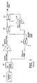
- FIG. 1 there is shown a simplified block diagram of an RF power amplifier system 100 which incorporates a feedforward system for improving the amplifier's linearity.
- a waveform source 102 communicates a source RF signal to an RF power divider 104.
- the RF power divider is conventionally used to split an RF source signal into two separate signals. Typically, each of these signals will have an RF power which is approximately half that of the source RF signal.
- the two signals thus produced include an amplifier input signal and a reference signal.
- the amplifier input signal is provided as an input to the RF power amplifier 106.
- a directional coupler 108 is conventionally used to obtain a low power sample of the distorted output signal from the RF power amplifier 106.
- the reference signal and the sampled output signal from the directional coupler 108 are communicated to separate inputs of a 180° hybrid RF signal combiner 114.
- the conventional 180° hybrid RF signal combiner subtracts the reference signal from the distorted amplifier output signal.
- the resulting output from the 180° hybrid RF signal combiner 114 is an error signal.
- the error signal is subsequently amplified in a linear error amplifier 116 so as to scale the error signal.
- the error signal is amplified so that its power level is properly scaled to equal the power level of any distortion contained in the distorted output signal from the RF power amplifier 106.
- the distorted output signal from the directional coupler is also communicated to a second directional coupler 110. In the second directional coupler 110, the error signal is combined with the distorted output signal in a subtraction operation. In particular, the RF error signal is subtracted from the distorted output signal of the RF power amplifier to remove the distortion from the output signal.
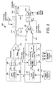
- FIG. 2 shows a simplified block diagram of an RF power amplifier system 200 with feedforward linearization incorporating a feedforward arrangement for removing non-linearities from the amplifier output.
- the arrangement shown is particularly useful for RF power amplifiers intended for use with wideband RF signals.
- the RF power amplifier system 200 includes a digital waveform source 202 that generates digital data signal s(t).
- the digital data signal s(t) can be a conventional complex source signal.
- a complex signal is any signal that is represented in terms of real and imaginary signal components.
- the digital data signal can be understood to be comprised of digital data that represents an analog signal comprised of in phase (I) and quadrature (Q) component vectors (I/Q component signal).
- Digital data of this type is well known in the art and therefore will not be described here in detail. Still, it should be understood that the invention is not limited in this regard. Instead, any other digital representation of a complex time varying analog signal can also be used.
- the digital waveform source 202 generates a signal which can be considered ideal in that it is an exact digital representation of the desired analog signal.
- the digital data signal s(t) lacks any distortion associated with conventional analog signal processing.
- the digital waveform source 202 can be realized in computer hardware, software, or a combination of hardware and software.
- the digital waveform source can be generated in one digital processing system, or in a distributed fashion where different processing elements are spread across several interconnected systems. Any kind of computer system, or other apparatus adapted for carrying out the methods described herein, is suited.
- a typical combination of hardware and software could be a general purpose computer processor or digital signal processor loaded with a computer program that controls the computer system such that it generates time varying digital representations of the I and Q signal components.
- Computer program or application in the present context means any expression, in any language, code or notation, of a set of instructions intended to cause a system having an information processing capability to perform a particular function either directly or after either or both of the following a) conversion to another language, code or notation; b) reproduction in a different material form.
- Reference signal generator block 203 includes at least one digital circuit which is capable of providing two identical outputs comprising the digital data signal s(t) from a single digital data signal s(t) input.
- a digital multiplexer or digital data buffer can be used for this purpose.
- the digital circuit is shown to be a digital multiplexer 204.
- the invention is not limited in this regard. All that is necessary is that some means be provided for generating two identical digital data signals s(t).
- the digital data signal s(t) is used to generate an analog signal which is used as an input to the amplifier 212.
- a first data conversion subsystem 213 is provided for this purpose.
- EER type amplifiers have separate processing paths for phase and amplitude information.
- phase and amplitude information For these types of amplifiers, it is necessary to convert an I/Q component signal to two analog signals that respectively represent amplitude and phase information. This amplitude and phase information is communicated to the EER amplifier as an input signal as is well known in the art.
- the digital data signal s(t) is communicated to first data conversion subsystem 213 which includes a signal format converter 206.
- the signal format converter would preferably be an I/Q to amplitude/phase (I/Q to A/P) converter.
- the signal format converter 206 converts the digital data signal s(t) (comprised of I and Q components) to an equivalent signal s'(t) in a different format.
- the equivalent signal s'(t) in this case is defined by a first component comprising a time varying amplitude signal A(t) and a second component comprised of a carrier signal that includes a time varying phase angle ⁇ (t). Converters of this type are well known in the art. Accordingly, signal format converter 206 will not be described in detail herein.
- the magnitude and phase components A(t) and ⁇ (t) can be in digital format. Such signals must be converted to an analog format before being communicated to the RF power amplifier 212.
- the first data conversion sub-system 213 can also include digital to analog converters.
- magnitude and phase components A(t) and ⁇ (t) are advantageously communicated to digital to analog (D/A) converters 208, 210. D/A converters are well known in the art and therefore will not be described here in detail.
- the power amplifier 212 can be a switching amplifier, which is also sometimes referred to as a Class D amplifier.
- the "magnitude" input is a baseband analog signal.
- the RF signal to be transmitted is generated in the power amplifier 212 and its amplitude modulation is controlled by the magnitude input signal.
- the "phase" input signal to power amplifier 212 controls the phase modulation of the RF signal that is generated by the power amplifier 212.
- the distorted RF output signal from power amplifier 212 will be communicated to a directional coupler 218.
- Directional coupler 218 includes an input port connected to the power amplifier 212, a transmitted port connected to a delay line 220, an isolated port connected to a termination resistor 224, and a coupled port connected to the differential amplifier 230.
- the directional coupler 218 will communicate most of the distorted RF output signal from power amplifier 212 to a time delay device 220.
- directional coupler 218 can be selected to be a 50 dB directional coupler. With such a coupler, the distorted RF output signal communicated to the time delay device 220 will generally be no more than about 1 dB below the power level of distorted output signal produced by the power amplifier 212. Still, it should be understood that the invention is not limited in this regard. Higher or lower power levels can be communicated to the differential amplifier 230 and the time delay device 220.
- Time delay device 220 compensates for the time-delays through differential amplifier 230, time delay device 232, and error amplifier 234.
- the time delay device 220 can be any device capable of producing a time delay in signals traversing through the time delay device.
- the time delay device 232 can be a simple RF delay line consisting of a length of RF transmission line.
- Time delay device 220 can also have a time-delay control circuit (not shown) which is responsive to a time delay control signal 221 for varying a time delay produced by time delay device 220.
- Such time delay control circuit can be in place of or in addition to a time delay control circuit (not shown) provided in time delay 232, which is responsive to a time delay control signal 233.
- Time delay control signals 215, 221, and 233 can be generated by an alignment processor 235 which monitors one or more signals to ensure timing alignment of the signals comprising the linearized output from coupler 222 .
- appropriate time delay control signals 215, 221, 233 can be determined by manual or automated means in an initial alignment process, and thereafter stored in a memory device.
- coupled signal 219 a portion of the distorted RF output signal from power amplifier 212 is coupled to the negative input of the differential amplifier 230.
- This signal shall be referred to herein as coupled signal 219.
- the coupled signal 219 will typically have a power level that is significantly reduced relative to the total RF input power communicated to the coupler 218 from the power amplifier 212.
- the actual power level of the coupled signal 219 will depend on a variety of design factors. However, the power level of coupled signal 219 will typically be no more than about 10% of the power level of the distorted output signal produced by the power amplifier 212.
- the directional coupler 218 can be a 50 dB type directional coupler so that the coupled signal will have a power level that is about 50 dB below the power level of the distorted RF output signal from the power amplifier 212. Still, it should be understood that the invention is not limited in this regard.
- a reference signal 229 is communicated to the positive input of the differential amplifier 230. This reference signal 229 is produced in reference signal generator 203, which will now be described in detail.
- the digital data signal s(t) provided from digital multiplexer 204 is communicated to a digital data time delay device 205 that is suitable for selectively delaying digital signals.
- the digital data time delay device 205 can be of the fixed delay type. However, the digital time delay device 205 can also include a time delay control circuit (not shown) which allows selective variable control of the amount of delay applied to digital data signal s(t).
- the time delay control circuit can be controlled by a time delay control signal 215 as shown.
- the digital time delay device 205 provides a time delay sufficient to ensure that the reference signal 229 is properly aligned in time with the coupled signal 219. This means that the path delays from the digital multiplexer 204 to the differential amplifier 230 are equalized for the reference signal 229 and the coupled signal 219.
- coupled signal 219 is delayed by the signal format converter 206, D/A converters 208, 210 and the power amplifier 212.
- the reference signal is delayed by the D/A converters 207, 209, and an RF modulator 211.
- the respective amounts of delay encountered by each signal can be different. Accordingly, in order to properly compare the coupled signal 219 to the reference signal 229, the signals must be aligned in time. This time alignment is performed by delay device 205.
- D/A converters 207, 209 which transforms the digital s(t) signal into an analog baseband signal.
- these signals can be analog baseband I and Q signals.
- RF modulator 211 which converts these analog baseband signals to an analog RF reference signal 229.
- the combination of D/A converters 207, 209 and the RF modulator 211 are referred to herein as the second data converting subsystem.
- RF modulator 211 can be implemented in the digital-domain, provided that the D/A converters can sample at twice the RF frequency. If the RF modulator is implemented in the digital-domain, then only one D/A is required.
- the analog RF reference signal 229 is an ideal reference signal in the sense that it is produced by an RF modulator 211 based on an exact digital representation of the desired source signal s(t) from digital waveform source 202. Also, it has been digitally delayed so as to provide correct time alignment. As such, it is absent of any significant distortion, such as the distortion caused by power amplifier 212.
- the power level of the coupled signal 219 and the analog RF reference signal 229 are preferably selected so that they are equal. For example, if the power amplifier 212 has an output power of +53 dBm and the directional coupler is a 50 dB directional coupler, then the coupled signal 219 will have a power level of +3 dBm. In this case, the analog RF reference signal 229 would also be selected to have a power level of +3 dBm. Of course, other power levels can also be used, but it is advantageous that the power level of the analog RF reference signal 229 and the coupled signal power level 219 are equal. When the power levels are arranged in this way, the output of the differential amplifier 230 will be an inverted error signal that represents the distortion introduced to the power amplifier 212.
- the inverted error signal output from the differential amplifier 230 is communicated to a time delay device 232.
- the time delay device 232 can be a fixed RF delay line consisting of a length of transmission line.
- the time delay device 232 can be selectively variable.
- a variable length transmission line can be used for this purpose.
- other types of delay lines are also possible and the invention is not intended to be limited in this regard.
- any one of a variety of commercially available variable analog delay line device can be used.
- the time delay device 232 can include at least one time delay control circuit for selectively varying the amount of time delay applied by the time delay device 232. As shown in FIG.
- a time delay control signal 233 can be provided as an input to the time delay device to selectively vary the time delay. Notably, it is not necessary to have time delay device 232.
- time delay device 232 allows the time-delay control to operate on lower-power signals, while the fixed time-delay 220 operates on the high-power signals.
- time delay device 232 can be removed and time-delay control provided for time-delay 220. Removing the time-delay device 232 allows less time-delay to be required by device 220.
- the inverted error signal output of the delay device 232 is communicated to at least one error amplifier 234.
- Error amplifier 234 is a linear amplifier which linearly amplifies the inverted error signal.
- a gain of the error amplifier can be adjustable by means of a gain adjustment control signal.
- the error amplifier 234 advantageously increases the power level of the inverted error signal so that it is equal to the power level of the distortion contained in the distorted amplifier output signal communicated to the directional coupler 222.
- the inverted error signal is communicated from an output of the error amplifier 234 to the input of directional coupler 222.
- directional couplers are well known in the art.
- the directional coupler 222 can be selected to be a 15 dB directional coupler.
- a 15dB coupling ratio for directional coupler 222 results in a minimal amount of RF power from power amplifier 212 being communicated to the termination resistor 226.
- the coupling is adequate for providing a sufficient amount of power from the error amplifier 234 to the linearized output signal from directional coupler 222 so as to substantially reduce distortion.
- the particular coupling ratio for directional coupler 222 can be chosen by the designer.
- the output power from error amplifier 234 should be chosen to ensure that the error signal produced by the error amplifier has sufficient magnitude to compensate for distortion contained in the output signal from the power amplifier 212.
- the directional coupler 222 is a four port device which couples the inverted error signal from error amplifier 234 to the distorted output signal.
- the directional coupler 222 produces a linearized output signal at an output port that is the sum of the distorted output signal and the inverted error signal. Since the error signal is inverted, the summing operation can be thought of as an operation which involves subtracting the error signal from the distorted output signal. Since the inverted error signal is an inverted representation of the distortion which is present in the distorted output signal, this subtracting operation removes the distortion that is present in the distorted output signal. The result is a linearized output.
- the present invention includes several features which together represent an important departure from the conventional feedforward type amplifier system of the prior as shown in FIG. 1 .
- One such feature concerns the way in which the reference signal 229 is processed.
- Conventional feedforward type amplifier systems similar to the one shown in FIG. 1 use an analog RF signal splitter 104 to generate a reference signal 229.
- analog RF signal splitters 104 when applied to a feedforward linearization system, such conventional analog RF signal splitters 104 have several undesirable characteristics. Most significantly, conventional analog RF signal splitters can exhibit frequency dependent phase and amplitude variations. Stated differently, this means that the transfer characteristic of the signal splitter 104 can introduce phase and amplitude variations over a bandwidth of an input signal.
- the present invention forms the reference signal by "splitting" the digital input signal s(t) while the signal is in the digital domain. This function is performed in digital multiplexer 204.
- the advantage of this approach is that it avoids the problem of phase and amplitude variations which typically occur over the bandwidth of an amplifier input signal when a conventional RF splitter is used. Such variations can be particularly problematic when the input signal is a wideband signal.
- Another advantage of the approach described herein is that it facilitates use of a digital data time delay device 205 which operates in the digital domain.
- Use of a digital data time delay device 205 in this feedforward linearization application is advantageous for several reasons.
- the digital data delay device 205 operates in the digital domain and therefore avoids any potential distortion of the reference signal which might otherwise occur if an analog delay device was used.
- variable time delay devices in the digital domain are relatively inexpensive, more easily implemented and digitally controlled. This is an advantage over variable analog time delay devices for RF signals.
- the use of a digital data time delay device 205 means that the linearization system can be rapidly reconfigured for use with different types of amplifiers 212.
- Different amplifiers 212 can have different time delays associated therewith.
- Use of a digital data delay device 205 for the reference signal means that the linearization system in FIG. 2 can be used with two or more amplifiers without any significant design modifications.
- conventional digital control signals can be communicated to the digital delay device 205 to control the time delay as needed for a particular application.
- control signals can be provided by a suitable integrated circuit controller or programmable ROM.
- Another important feature of the present invention concerns the manner in which the coupled signal 219 is subtracted from the reference signal 229.
- the present invention makes use of a differential amplifier 230 in place of a conventional 180° hybrid coupler 114 as shown in FIG. 1 .
- Conventional 180° hybrid couplers suffer from two potential problems. First, 180° hybrid couples can and do exhibit frequency dependent variations in phase and amplitude. Such variations can be particularly problematic when the input signals to the 180° hybrid coupler is used to process signals having a relatively wide bandwidth. It will be appreciated by those skilled in the art that frequency dependent variations in phase and amplitude can produce distortion which will result in an inverted error signal which is inaccurate. In such case, the error signal can fail to properly improve the linearity of the output signal from power amplifier 212 because the error signal does not accurately represent the error.
- CMRR common mode rejection ratio
- the common-mode rejection ratio (CMRR) of a device is a measure of that device's tendency to reject input signals common to both inputs.
- the CMRR refers to the ability of a 180° hybrid coupler 114 (or the differential amplifier 230) to completely and accurately determine the difference between a reference signal and a distorted amplifier output signal.
- a high CMRR is important in feedforward linearization applications because the distortion existing in the distorted amplifier output signal can often be a relatively small voltage compared to the amplitude of the distorted amplifier output signal.
- the differential amplifier 230 should have a design which results in a common mode rejection ratio (CMRR) of at least about 50 dB.
- CMRR common mode rejection ratio
- the differential amplifier should preferably have a bandwidth that is suitable for a range of input frequencies that are contained in the reference signal 229.
- CMRR common mode rejection ratio
- the amplifier system 200 is intended for use with conventional broadcast signals in the AM or FM broadcast band, a linear differential amplifier having a bandwidth of between 10 MHz and 200 MHz can be used.
- the precise specification for the degree of linearity required of differential amplifier 230 will depend upon the level of the distortion to be eliminated from power amplifier 212.
- the differential amplifier 230 must be sufficiently free from distortion so that the amplifier can accurately generate an error signal based on a difference between the reference signal 229 and the coupled signal 219.
- the amplifier system described herein can be used for a wide variety of signals, including broadband data signal.
- differential amplifier 230 and error amplifier 234 have a suitably wide operational bandwidth.
- the differential amplifier 230 can be a conventional integrated circuit device, a hybrid circuit design, or an RF type differential amplifier.
- the particular type of circuit construction will be determined by the CMRR and bandwidth capability required in a particular application for processing particular types of broadband signals.
Landscapes
- Physics & Mathematics (AREA)
- Nonlinear Science (AREA)
- Engineering & Computer Science (AREA)
- Power Engineering (AREA)
- Amplifiers (AREA)
- Transmitters (AREA)
Claims (9)
- HF-Verstärkersystem (200) mit Feedforward-Linearisierung, das umfasst:- einen digitalen Multiplexer (204), der dafür konfiguriert ist, digitale Daten s(t) von einer digitalen Wellenformquelle (202) zu empfangen und erste und zweite Instanzen der digitalen Daten zu generieren,- eine erste Umsetzeinrichtung (213), die mit dem digitalen Multiplexer verbunden ist, um die erste Instanz der digitalen Daten in analoge Größen- und Phasensignale umzusetzen, die das analoge Signal definieren,- einen HF-Verstärker (212), der mit der ersten Umsetzeinrichtung verbunden ist und auf die Größen- und Phasensignale anspricht, um ein durch wenigstens eines der Größen- und Phasensignale moduliertes, verzerrtes HF-Ausgangssignal zu generieren,- eine Digitaldaten-Zeitverzögerungseinrichtung (205), die mit dem digitalen Multiplexer (204) verbunden und dafür konfiguriert ist, die zweite Instanz der digitalen Daten gemäß einem Zeitverzögerungssteuersignal (215) von einem Abgleich-Prozessor (235) selektiv variabel zu verzögern,- eine zweite Umsetzeinrichtung (207, 209, 211), die dafür konfiguriert ist, die zweite Instanz der digitalen Daten von der Digitaldaten-Zeitverzögerungseinrichtung (205) zu empfangen und die zweite Instanz der digitalen Daten in ein analoges HF-Referenzsignal umzusetzen,- eine Feedforward-Linearisierungsschaltung (218, 219, 230) zum Reduzieren einer Verzerrung des HF-Verstärkers, wobei die Feedforward-Linearisierungsschaltung einen Differenzverstärker (230) umfasst, der dafür eingerichtet ist, ein Fehlersignal zu generieren, das eine Differenz zwischen dem verzerrten HF-Ausgangssignal und dem analogen HF-Referenzsignal repräsentiert,- eine Kombinationseinrichtung (222) zum Kombinieren des Fehlersignals mit dem verzerrten HF-Ausgangssignal, um einen verzerrten Abschnitt des verzerrten HF-Ausgangssignals zu beseitigen.
- HF-Verstärkersystem nach Anspruch 1, wobei die digitalen Daten ein digitales I/Q-Komponentensignal darstellen und die erste Umsetzeinrichtung einen Signalformatumsetzer (206) umfasst, der dafür eingerichtet ist, das digitale I/Q-Komponentensignal in wenigstens ein digitales Datensignal umzusetzen, das Phasen- und Größeninformationen enthält.
- HF-Verstärkersystem nach Anspruch 2, wobei die erste Umsetzeinrichtung ferner zumindest einen Digital-Analog-Umsetzer (208, 210) umfasst, der mit dem Signalformatumsetzer verbunden und dafür konfiguriert ist, das wenigstens eine Phasen- und Größeninformationen enthaltende digitale Datensignal in die analogen Größen- und Phasensignale umzusetzen.
- HF-Verstärkersystem nach Anspruch 1, wobei die zweite Umsetzeinrichtung zumindest einen Digital-Analog-Umsetzer (207, 209) umfasst, der dafür konfiguriert ist, anhand der zweiten Instanz der digitalen Daten analoge Basisband-I- und Q-Komponenten zu generieren.
- HF-Verstärkersystem nach Anspruch 4, wobei die zweite Umsetzeinrichtung ferner einen HF-Modulator (211) umfasst, der mit dem zumindest einen Digital-Analog-Umsetzer verbunden ist und auf die Basisband-I- und Q-Komponenten des analogen Referenzsignals anspricht, um das analoge HF-Referenzsignal zu generieren.
- HF-Verstärkersystem nach Anspruch 1, der ferner einen Fehlerverstärker (234) mit einem Eingang, der dafür konfiguriert ist, das Fehlersignal vom Differenzverstärker zu empfangen, und einem Ausgang aufweist, der mit der Kombinationseinrichtung verbunden ist, wobei der Fehlerverstärker dafür konfiguriert ist, das Fehlersignal zu verstärken.
- HF-Verstärkersystem nach Anspruch 1, das ferner eine analoge Zeitverzögerungseinrichtung (232) umfasst, die mit dem Differenzverstärker und/oder dem Fehlerverstärker verbunden ist, wobei die analoge Zeitverzögerungseinrichtung dafür konfiguriert ist, das Fehlersignal selektiv zu verzögern.
- HF-Verstärkersystem nach Anspruch 1, wobei der HF-Verstärker ein EER-Verstärker ist.
- Verfahren zum Linearisieren eines Ausgangssignals eines HF-Verstärkers, das umfasst:- Generieren erster und zweiter Instanzen digitaler Daten s(t) unter Verwendung eines digitalen Multiplexers (204),- Umsetzen der ersten Instanz der digitalen Daten in analoge Größen- und Phasensignale,- Generieren eines durch wenigstens eines der Größen- und Phasensignale modulierten, verzerrten HF-Ausgangssignals unter Verwendung eines HF-Verstärkers (212), der auf die Größen- und Phasensignale anspricht,- Umsetzen der zweiten Instanz der digitalen Daten in ein analoges HF-Referenzsignal,- Reduzieren einer Verzerrung des verzerrten HF-Ausgangssignals unter Verwendung einer Feedforward-Linearisierungsschaltung (218, 219, 230), die ein Fehlersignal generiert, das eine Differenz zwischen dem verzerrten HF-Ausgangssignal und dem analogen HF-Referenzsignal repräsentiert, und das Fehlersignal mit dem verzerrten HF-Ausgangssignal kombiniert, um einen verzerrten Abschnitt des verzerrten HF-Ausgangssignals zu beseitigen und wenigstens ein linearisiertes Ausgangssignal zu generieren,- wobei das Reduzieren ferner das Überwachen des verzerrten HF-Ausgangssignals und des analogen HF-Referenzsignals sowie das Generieren eines Zeitverzögerungssignals basierend auf der Überwachung umfasst, um die zweite Instanz der digitalen Daten zeitlich zu verzögern, um einen Zeitabgleich für das Generieren des linearisierten Ausgangssignals sicherzustellen.
Applications Claiming Priority (2)
| Application Number | Priority Date | Filing Date | Title |
|---|---|---|---|
| US12/061,013 US7642850B2 (en) | 2008-04-02 | 2008-04-02 | Feedforward linearization of RF power amplifiers |
| PCT/US2009/038867 WO2009123999A1 (en) | 2008-04-02 | 2009-03-31 | Feedforward linearization of rf power amplifiers |
Publications (2)
| Publication Number | Publication Date |
|---|---|
| EP2277262A1 EP2277262A1 (de) | 2011-01-26 |
| EP2277262B1 true EP2277262B1 (de) | 2013-11-13 |
Family
ID=40673449
Family Applications (1)
| Application Number | Title | Priority Date | Filing Date |
|---|---|---|---|
| EP09726729.8A Not-in-force EP2277262B1 (de) | 2008-04-02 | 2009-03-31 | Vorwärtskopplungslinearisierung von hf-leistungsverstärkern |
Country Status (7)
| Country | Link |
|---|---|
| US (1) | US7642850B2 (de) |
| EP (1) | EP2277262B1 (de) |
| JP (1) | JP2011517215A (de) |
| KR (1) | KR101102109B1 (de) |
| CA (1) | CA2720162C (de) |
| TW (1) | TWI442697B (de) |
| WO (1) | WO2009123999A1 (de) |
Families Citing this family (7)
| Publication number | Priority date | Publication date | Assignee | Title |
|---|---|---|---|---|
| FR2920265A1 (fr) * | 2007-08-23 | 2009-02-27 | Eads Secure Networks Soc Par A | Correction de distorsions dans une chaine d'emission |
| US8254493B2 (en) * | 2008-09-30 | 2012-08-28 | Intel Mobile Communications GmbH | High bandwidth modulation and transmission |
| US9077440B2 (en) * | 2013-01-04 | 2015-07-07 | Telefonaktiebolaget L M Ericsson (Publ) | Digital suppression of transmitter intermodulation in receiver |
| US9214968B2 (en) * | 2013-07-24 | 2015-12-15 | Nokia Technologies Oy | Apparatus and methods for providing a power amplifier with interference cancellation |
| US11108403B2 (en) * | 2017-04-13 | 2021-08-31 | Rohde & Schwarz Gmbh & Co. Kg | Device and method for efficient digital-analog conversion |
| TWI696344B (zh) * | 2018-11-16 | 2020-06-11 | 財團法人工業技術研究院 | 線性度改善系統及線性度改善方法 |
| CN112285620B (zh) | 2019-07-24 | 2024-09-06 | 通用电气精准医疗有限责任公司 | Rf发射系统和方法、mri系统及其预扫描方法以及存储介质 |
Family Cites Families (25)
| Publication number | Priority date | Publication date | Assignee | Title |
|---|---|---|---|---|
| GB9002788D0 (en) * | 1990-02-08 | 1990-04-04 | Marconi Co Ltd | Circuit for reducing distortion produced by an r.f.power amplifier |
| US5892397A (en) | 1996-03-29 | 1999-04-06 | Spectrian | Adaptive compensation of RF amplifier distortion by injecting predistortion signal derived from respectively different functions of input signal amplitude |
| US5923712A (en) | 1997-05-05 | 1999-07-13 | Glenayre Electronics, Inc. | Method and apparatus for linear transmission by direct inverse modeling |
| US5861777A (en) | 1997-07-02 | 1999-01-19 | Motorola, Inc. | Method and apparatus for compensation of phase distortion in power amplifiers |
| FI105366B (fi) | 1997-10-29 | 2000-07-31 | Nokia Networks Oy | Linearisointimenetelmä ja vahvistinjärjestely |
| US5959500A (en) * | 1998-01-26 | 1999-09-28 | Glenayre Electronics, Inc. | Model-based adaptive feedforward amplifier linearizer |
| US6078216A (en) | 1998-03-31 | 2000-06-20 | Spectrian Corporation | Aliased wide band performance monitor for adjusting predistortion and vector modulator control parameters of RF amplifier |
| US6188732B1 (en) | 1998-10-19 | 2001-02-13 | Samsung Electronics Co., Ltd. | Digital feedforward amplifier for use in an RF transmitter and method of operation |
| GB2351624B (en) | 1999-06-30 | 2003-12-03 | Wireless Systems Int Ltd | Reducing distortion of signals |
| US6356146B1 (en) | 1999-07-13 | 2002-03-12 | Pmc-Sierra, Inc. | Amplifier measurement and modeling processes for use in generating predistortion parameters |
| KR100674586B1 (ko) | 1999-12-30 | 2007-01-25 | 엘지전자 주식회사 | 전력증폭기의 전치왜곡 선형화기 |
| US6570444B2 (en) | 2000-01-26 | 2003-05-27 | Pmc-Sierra, Inc. | Low noise wideband digital predistortion amplifier |
| US6944238B2 (en) | 2001-02-16 | 2005-09-13 | Lucent Technologies Inc. | Digital transmitter system and method |
| US6794936B2 (en) | 2001-07-03 | 2004-09-21 | Lucent Technologies Inc. | Equalizer system and method for predistortion |
| US6756844B2 (en) | 2001-08-07 | 2004-06-29 | Hitachi Kokusai Electric Inc. | Distortion compensation amplification apparatus of feed forward type and adaptive pre-distortion type |
| JP3805221B2 (ja) | 2001-09-18 | 2006-08-02 | 株式会社日立国際電気 | 歪み補償装置 |
| US6834084B2 (en) | 2002-05-06 | 2004-12-21 | Rf Micro Devices Inc | Direct digital polar modulator |
| US6937669B2 (en) | 2002-12-03 | 2005-08-30 | Motorola, Inc. | Digital predistortion system for linearizing a power amplifier |
| US7129778B2 (en) | 2003-07-23 | 2006-10-31 | Northrop Grumman Corporation | Digital cross cancellation system |
| US7034614B2 (en) * | 2003-11-21 | 2006-04-25 | Northrop Grumman Corporation | Modified polar amplifier architecture |
| JP4443514B2 (ja) | 2003-11-24 | 2010-03-31 | テレフオンアクチーボラゲット エル エム エリクソン(パブル) | 受信信号を処理する装置及び方法 |
| US7336725B2 (en) | 2004-03-03 | 2008-02-26 | Powerwave Technologies, Inc. | Digital predistortion system and method for high efficiency transmitters |
| JP2006093873A (ja) * | 2004-09-21 | 2006-04-06 | Matsushita Electric Ind Co Ltd | Eer変調増幅装置 |
| DE602006000525T2 (de) | 2005-06-03 | 2009-02-05 | Ntt Docomo Inc. | Mehrbandvorverzerrer mit Korrekturwertetabellen |
| JP2007221418A (ja) * | 2006-02-16 | 2007-08-30 | Matsushita Electric Ind Co Ltd | Eerシステムを用いた電力増幅装置および電力増幅方法 |
-
2008
- 2008-04-02 US US12/061,013 patent/US7642850B2/en active Active
-
2009
- 2009-03-31 JP JP2011503086A patent/JP2011517215A/ja active Pending
- 2009-03-31 EP EP09726729.8A patent/EP2277262B1/de not_active Not-in-force
- 2009-03-31 CA CA2720162A patent/CA2720162C/en not_active Expired - Fee Related
- 2009-03-31 WO PCT/US2009/038867 patent/WO2009123999A1/en not_active Ceased
- 2009-03-31 KR KR1020107024349A patent/KR101102109B1/ko not_active Expired - Fee Related
- 2009-04-01 TW TW098110916A patent/TWI442697B/zh not_active IP Right Cessation
Also Published As
| Publication number | Publication date |
|---|---|
| US7642850B2 (en) | 2010-01-05 |
| CA2720162A1 (en) | 2009-10-08 |
| US20090251211A1 (en) | 2009-10-08 |
| TW201004131A (en) | 2010-01-16 |
| JP2011517215A (ja) | 2011-05-26 |
| KR101102109B1 (ko) | 2012-01-02 |
| EP2277262A1 (de) | 2011-01-26 |
| TWI442697B (zh) | 2014-06-21 |
| CA2720162C (en) | 2014-01-28 |
| WO2009123999A1 (en) | 2009-10-08 |
| KR20100127866A (ko) | 2010-12-06 |
Similar Documents
| Publication | Publication Date | Title |
|---|---|---|
| CN101156159B (zh) | 用于高效率发射机的数字预失真系统和方法 | |
| CN102437822B (zh) | 一种射频功率放大器自适应数字预失真线性化系统 | |
| US7366252B2 (en) | Wideband enhanced digital injection predistortion system and method | |
| JP4033794B2 (ja) | 高効率線形電力増幅器 | |
| EP2277262B1 (de) | Vorwärtskopplungslinearisierung von hf-leistungsverstärkern | |
| US20080111622A1 (en) | Hybrid Doherty Amplifier System and Method | |
| EP1011192A2 (de) | Lineare Verstärkeranordnung | |
| JP2002522989A (ja) | 移動通信システムの電力増幅線形化装置及び方法 | |
| EP1042864A1 (de) | Verfahren und vorrichtung für breitbandvorverzerrungslinearisierung | |
| KR100438445B1 (ko) | 비선형 왜곡 보상 방법 및 비선형 왜곡 보상 회로 | |
| JP2005117599A (ja) | 高周波増幅器 | |
| JP2012085295A (ja) | 電力増幅器線形化方法及び装置 | |
| KR20020008456A (ko) | 피드포워드 방식의 선형화기를 갖는 기지국 송신장치 | |
| CN107579716A (zh) | 基于模拟对消的线性功率放大器 | |
| US7769103B2 (en) | Amplifier system employing analog polynomial predistortion with sub-nyquist digital adaptation | |
| KR20050039659A (ko) | 합성 룩업 테이블들에 기초하여 사전왜곡 처리하는 증폭기 | |
| KR20020052495A (ko) | 알에프 전력증폭기의 디지탈 선형화장치 | |
| KR20020054150A (ko) | 선형화기의 왜곡 보정 회로 | |
| Jeon | A Study on Feedforward System for IMT-2000 | |
| HK1211391B (en) | Extended bandwidth digital doherty transmitter | |
| HK1211391A1 (en) | Extended bandwidth digital doherty transmitter |
Legal Events
| Date | Code | Title | Description |
|---|---|---|---|
| PUAI | Public reference made under article 153(3) epc to a published international application that has entered the european phase |
Free format text: ORIGINAL CODE: 0009012 |
|
| 17P | Request for examination filed |
Effective date: 20101026 |
|
| AK | Designated contracting states |
Kind code of ref document: A1 Designated state(s): AT BE BG CH CY CZ DE DK EE ES FI FR GB GR HR HU IE IS IT LI LT LU LV MC MK MT NL NO PL PT RO SE SI SK TR |
|
| AX | Request for extension of the european patent |
Extension state: AL BA RS |
|
| RIN1 | Information on inventor provided before grant (corrected) |
Inventor name: MOFFATT , CHRISTOPHER D . Inventor name: TONTI , JAMES Inventor name: MARTIN, G., PATRICK |
|
| DAX | Request for extension of the european patent (deleted) | ||
| GRAP | Despatch of communication of intention to grant a patent |
Free format text: ORIGINAL CODE: EPIDOSNIGR1 |
|
| INTG | Intention to grant announced |
Effective date: 20130522 |
|
| GRAS | Grant fee paid |
Free format text: ORIGINAL CODE: EPIDOSNIGR3 |
|
| GRAP | Despatch of communication of intention to grant a patent |
Free format text: ORIGINAL CODE: EPIDOSNIGR1 |
|
| GRAA | (expected) grant |
Free format text: ORIGINAL CODE: 0009210 |
|
| INTG | Intention to grant announced |
Effective date: 20130920 |
|
| AK | Designated contracting states |
Kind code of ref document: B1 Designated state(s): AT BE BG CH CY CZ DE DK EE ES FI FR GB GR HR HU IE IS IT LI LT LU LV MC MK MT NL NO PL PT RO SE SI SK TR |
|
| REG | Reference to a national code |
Ref country code: GB Ref legal event code: FG4D |
|
| REG | Reference to a national code |
Ref country code: CH Ref legal event code: EP |
|
| REG | Reference to a national code |
Ref country code: AT Ref legal event code: REF Ref document number: 640957 Country of ref document: AT Kind code of ref document: T Effective date: 20131215 |
|
| REG | Reference to a national code |
Ref country code: IE Ref legal event code: FG4D |
|
| REG | Reference to a national code |
Ref country code: DE Ref legal event code: R096 Ref document number: 602009020071 Country of ref document: DE Effective date: 20140109 |
|
| REG | Reference to a national code |
Ref country code: NL Ref legal event code: VDEP Effective date: 20131113 |
|
| REG | Reference to a national code |
Ref country code: AT Ref legal event code: MK05 Ref document number: 640957 Country of ref document: AT Kind code of ref document: T Effective date: 20131113 |
|
| REG | Reference to a national code |
Ref country code: LT Ref legal event code: MG4D |
|
| PG25 | Lapsed in a contracting state [announced via postgrant information from national office to epo] |
Ref country code: NL Free format text: LAPSE BECAUSE OF FAILURE TO SUBMIT A TRANSLATION OF THE DESCRIPTION OR TO PAY THE FEE WITHIN THE PRESCRIBED TIME-LIMIT Effective date: 20131113 Ref country code: NO Free format text: LAPSE BECAUSE OF FAILURE TO SUBMIT A TRANSLATION OF THE DESCRIPTION OR TO PAY THE FEE WITHIN THE PRESCRIBED TIME-LIMIT Effective date: 20140213 Ref country code: HR Free format text: LAPSE BECAUSE OF FAILURE TO SUBMIT A TRANSLATION OF THE DESCRIPTION OR TO PAY THE FEE WITHIN THE PRESCRIBED TIME-LIMIT Effective date: 20131113 Ref country code: IS Free format text: LAPSE BECAUSE OF FAILURE TO SUBMIT A TRANSLATION OF THE DESCRIPTION OR TO PAY THE FEE WITHIN THE PRESCRIBED TIME-LIMIT Effective date: 20140313 Ref country code: FI Free format text: LAPSE BECAUSE OF FAILURE TO SUBMIT A TRANSLATION OF THE DESCRIPTION OR TO PAY THE FEE WITHIN THE PRESCRIBED TIME-LIMIT Effective date: 20131113 Ref country code: SE Free format text: LAPSE BECAUSE OF FAILURE TO SUBMIT A TRANSLATION OF THE DESCRIPTION OR TO PAY THE FEE WITHIN THE PRESCRIBED TIME-LIMIT Effective date: 20131113 Ref country code: LT Free format text: LAPSE BECAUSE OF FAILURE TO SUBMIT A TRANSLATION OF THE DESCRIPTION OR TO PAY THE FEE WITHIN THE PRESCRIBED TIME-LIMIT Effective date: 20131113 |
|
| PG25 | Lapsed in a contracting state [announced via postgrant information from national office to epo] |
Ref country code: CY Free format text: LAPSE BECAUSE OF FAILURE TO SUBMIT A TRANSLATION OF THE DESCRIPTION OR TO PAY THE FEE WITHIN THE PRESCRIBED TIME-LIMIT Effective date: 20131113 Ref country code: ES Free format text: LAPSE BECAUSE OF FAILURE TO SUBMIT A TRANSLATION OF THE DESCRIPTION OR TO PAY THE FEE WITHIN THE PRESCRIBED TIME-LIMIT Effective date: 20131113 Ref country code: AT Free format text: LAPSE BECAUSE OF FAILURE TO SUBMIT A TRANSLATION OF THE DESCRIPTION OR TO PAY THE FEE WITHIN THE PRESCRIBED TIME-LIMIT Effective date: 20131113 Ref country code: LV Free format text: LAPSE BECAUSE OF FAILURE TO SUBMIT A TRANSLATION OF THE DESCRIPTION OR TO PAY THE FEE WITHIN THE PRESCRIBED TIME-LIMIT Effective date: 20131113 Ref country code: BE Free format text: LAPSE BECAUSE OF FAILURE TO SUBMIT A TRANSLATION OF THE DESCRIPTION OR TO PAY THE FEE WITHIN THE PRESCRIBED TIME-LIMIT Effective date: 20131113 |
|
| PG25 | Lapsed in a contracting state [announced via postgrant information from national office to epo] |
Ref country code: PT Free format text: LAPSE BECAUSE OF FAILURE TO SUBMIT A TRANSLATION OF THE DESCRIPTION OR TO PAY THE FEE WITHIN THE PRESCRIBED TIME-LIMIT Effective date: 20140313 |
|
| PG25 | Lapsed in a contracting state [announced via postgrant information from national office to epo] |
Ref country code: EE Free format text: LAPSE BECAUSE OF FAILURE TO SUBMIT A TRANSLATION OF THE DESCRIPTION OR TO PAY THE FEE WITHIN THE PRESCRIBED TIME-LIMIT Effective date: 20131113 |
|
| REG | Reference to a national code |
Ref country code: DE Ref legal event code: R097 Ref document number: 602009020071 Country of ref document: DE |
|
| PG25 | Lapsed in a contracting state [announced via postgrant information from national office to epo] |
Ref country code: RO Free format text: LAPSE BECAUSE OF FAILURE TO SUBMIT A TRANSLATION OF THE DESCRIPTION OR TO PAY THE FEE WITHIN THE PRESCRIBED TIME-LIMIT Effective date: 20131113 Ref country code: SK Free format text: LAPSE BECAUSE OF FAILURE TO SUBMIT A TRANSLATION OF THE DESCRIPTION OR TO PAY THE FEE WITHIN THE PRESCRIBED TIME-LIMIT Effective date: 20131113 Ref country code: PL Free format text: LAPSE BECAUSE OF FAILURE TO SUBMIT A TRANSLATION OF THE DESCRIPTION OR TO PAY THE FEE WITHIN THE PRESCRIBED TIME-LIMIT Effective date: 20131113 Ref country code: CZ Free format text: LAPSE BECAUSE OF FAILURE TO SUBMIT A TRANSLATION OF THE DESCRIPTION OR TO PAY THE FEE WITHIN THE PRESCRIBED TIME-LIMIT Effective date: 20131113 |
|
| PLBE | No opposition filed within time limit |
Free format text: ORIGINAL CODE: 0009261 |
|
| STAA | Information on the status of an ep patent application or granted ep patent |
Free format text: STATUS: NO OPPOSITION FILED WITHIN TIME LIMIT |
|
| PG25 | Lapsed in a contracting state [announced via postgrant information from national office to epo] |
Ref country code: DK Free format text: LAPSE BECAUSE OF FAILURE TO SUBMIT A TRANSLATION OF THE DESCRIPTION OR TO PAY THE FEE WITHIN THE PRESCRIBED TIME-LIMIT Effective date: 20131113 |
|
| 26N | No opposition filed |
Effective date: 20140814 |
|
| PG25 | Lapsed in a contracting state [announced via postgrant information from national office to epo] |
Ref country code: LU Free format text: LAPSE BECAUSE OF FAILURE TO SUBMIT A TRANSLATION OF THE DESCRIPTION OR TO PAY THE FEE WITHIN THE PRESCRIBED TIME-LIMIT Effective date: 20140331 |
|
| REG | Reference to a national code |
Ref country code: CH Ref legal event code: PL |
|
| REG | Reference to a national code |
Ref country code: DE Ref legal event code: R097 Ref document number: 602009020071 Country of ref document: DE Effective date: 20140814 |
|
| REG | Reference to a national code |
Ref country code: IE Ref legal event code: MM4A |
|
| PG25 | Lapsed in a contracting state [announced via postgrant information from national office to epo] |
Ref country code: CH Free format text: LAPSE BECAUSE OF NON-PAYMENT OF DUE FEES Effective date: 20140331 Ref country code: IE Free format text: LAPSE BECAUSE OF NON-PAYMENT OF DUE FEES Effective date: 20140331 Ref country code: LI Free format text: LAPSE BECAUSE OF NON-PAYMENT OF DUE FEES Effective date: 20140331 |
|
| PG25 | Lapsed in a contracting state [announced via postgrant information from national office to epo] |
Ref country code: SI Free format text: LAPSE BECAUSE OF FAILURE TO SUBMIT A TRANSLATION OF THE DESCRIPTION OR TO PAY THE FEE WITHIN THE PRESCRIBED TIME-LIMIT Effective date: 20131113 |
|
| REG | Reference to a national code |
Ref country code: FR Ref legal event code: PLFP Year of fee payment: 7 |
|
| PG25 | Lapsed in a contracting state [announced via postgrant information from national office to epo] |
Ref country code: IT Free format text: LAPSE BECAUSE OF FAILURE TO SUBMIT A TRANSLATION OF THE DESCRIPTION OR TO PAY THE FEE WITHIN THE PRESCRIBED TIME-LIMIT Effective date: 20131113 |
|
| PGFP | Annual fee paid to national office [announced via postgrant information from national office to epo] |
Ref country code: FR Payment date: 20150317 Year of fee payment: 7 Ref country code: GB Payment date: 20150327 Year of fee payment: 7 |
|
| PG25 | Lapsed in a contracting state [announced via postgrant information from national office to epo] |
Ref country code: MT Free format text: LAPSE BECAUSE OF FAILURE TO SUBMIT A TRANSLATION OF THE DESCRIPTION OR TO PAY THE FEE WITHIN THE PRESCRIBED TIME-LIMIT Effective date: 20131113 |
|
| PG25 | Lapsed in a contracting state [announced via postgrant information from national office to epo] |
Ref country code: MC Free format text: LAPSE BECAUSE OF FAILURE TO SUBMIT A TRANSLATION OF THE DESCRIPTION OR TO PAY THE FEE WITHIN THE PRESCRIBED TIME-LIMIT Effective date: 20131113 |
|
| PG25 | Lapsed in a contracting state [announced via postgrant information from national office to epo] |
Ref country code: GR Free format text: LAPSE BECAUSE OF FAILURE TO SUBMIT A TRANSLATION OF THE DESCRIPTION OR TO PAY THE FEE WITHIN THE PRESCRIBED TIME-LIMIT Effective date: 20140214 Ref country code: BG Free format text: LAPSE BECAUSE OF FAILURE TO SUBMIT A TRANSLATION OF THE DESCRIPTION OR TO PAY THE FEE WITHIN THE PRESCRIBED TIME-LIMIT Effective date: 20131113 |
|
| PG25 | Lapsed in a contracting state [announced via postgrant information from national office to epo] |
Ref country code: TR Free format text: LAPSE BECAUSE OF FAILURE TO SUBMIT A TRANSLATION OF THE DESCRIPTION OR TO PAY THE FEE WITHIN THE PRESCRIBED TIME-LIMIT Effective date: 20131113 Ref country code: HU Free format text: LAPSE BECAUSE OF FAILURE TO SUBMIT A TRANSLATION OF THE DESCRIPTION OR TO PAY THE FEE WITHIN THE PRESCRIBED TIME-LIMIT; INVALID AB INITIO Effective date: 20090331 |
|
| GBPC | Gb: european patent ceased through non-payment of renewal fee |
Effective date: 20160331 |
|
| REG | Reference to a national code |
Ref country code: FR Ref legal event code: ST Effective date: 20161130 |
|
| PG25 | Lapsed in a contracting state [announced via postgrant information from national office to epo] |
Ref country code: GB Free format text: LAPSE BECAUSE OF NON-PAYMENT OF DUE FEES Effective date: 20160331 Ref country code: FR Free format text: LAPSE BECAUSE OF NON-PAYMENT OF DUE FEES Effective date: 20160331 |
|
| PG25 | Lapsed in a contracting state [announced via postgrant information from national office to epo] |
Ref country code: MK Free format text: LAPSE BECAUSE OF FAILURE TO SUBMIT A TRANSLATION OF THE DESCRIPTION OR TO PAY THE FEE WITHIN THE PRESCRIBED TIME-LIMIT Effective date: 20131113 |
|
| PGFP | Annual fee paid to national office [announced via postgrant information from national office to epo] |
Ref country code: DE Payment date: 20230207 Year of fee payment: 15 |
|
| REG | Reference to a national code |
Ref country code: DE Ref legal event code: R119 Ref document number: 602009020071 Country of ref document: DE |
|
| PG25 | Lapsed in a contracting state [announced via postgrant information from national office to epo] |
Ref country code: DE Free format text: LAPSE BECAUSE OF NON-PAYMENT OF DUE FEES Effective date: 20241001 |
|
| PG25 | Lapsed in a contracting state [announced via postgrant information from national office to epo] |
Ref country code: DE Free format text: LAPSE BECAUSE OF NON-PAYMENT OF DUE FEES Effective date: 20241001 |