EP2277232B1 - Wellenleiterübergangsanordnung - Google Patents
Wellenleiterübergangsanordnung Download PDFInfo
- Publication number
- EP2277232B1 EP2277232B1 EP08741917.2A EP08741917A EP2277232B1 EP 2277232 B1 EP2277232 B1 EP 2277232B1 EP 08741917 A EP08741917 A EP 08741917A EP 2277232 B1 EP2277232 B1 EP 2277232B1
- Authority
- EP
- European Patent Office
- Prior art keywords
- waveguide
- bend
- aperture
- carrier material
- metalization
- Prior art date
- Legal status (The legal status is an assumption and is not a legal conclusion. Google has not performed a legal analysis and makes no representation as to the accuracy of the status listed.)
- Active
Links
Images

Classifications
-
- H—ELECTRICITY
- H05—ELECTRIC TECHNIQUES NOT OTHERWISE PROVIDED FOR
- H05K—PRINTED CIRCUITS; CASINGS OR CONSTRUCTIONAL DETAILS OF ELECTRIC APPARATUS; MANUFACTURE OF ASSEMBLAGES OF ELECTRICAL COMPONENTS
- H05K1/00—Printed circuits
- H05K1/02—Details
- H05K1/0213—Electrical arrangements not otherwise provided for
- H05K1/0237—High frequency adaptations
- H05K1/0243—Printed circuits associated with mounted high frequency components
-
- H—ELECTRICITY
- H01—ELECTRIC ELEMENTS
- H01P—WAVEGUIDES; RESONATORS, LINES, OR OTHER DEVICES OF THE WAVEGUIDE TYPE
- H01P1/00—Auxiliary devices
- H01P1/02—Bends; Corners; Twists
- H01P1/022—Bends; Corners; Twists in waveguides of polygonal cross-section
- H01P1/025—Bends; Corners; Twists in waveguides of polygonal cross-section in the E-plane
-
- H—ELECTRICITY
- H01—ELECTRIC ELEMENTS
- H01P—WAVEGUIDES; RESONATORS, LINES, OR OTHER DEVICES OF THE WAVEGUIDE TYPE
- H01P5/00—Coupling devices of the waveguide type
- H01P5/02—Coupling devices of the waveguide type with invariable factor of coupling
-
- H—ELECTRICITY
- H01—ELECTRIC ELEMENTS
- H01P—WAVEGUIDES; RESONATORS, LINES, OR OTHER DEVICES OF THE WAVEGUIDE TYPE
- H01P5/00—Coupling devices of the waveguide type
- H01P5/02—Coupling devices of the waveguide type with invariable factor of coupling
- H01P5/022—Transitions between lines of the same kind and shape, but with different dimensions
- H01P5/024—Transitions between lines of the same kind and shape, but with different dimensions between hollow waveguides
-
- H—ELECTRICITY
- H01—ELECTRIC ELEMENTS
- H01P—WAVEGUIDES; RESONATORS, LINES, OR OTHER DEVICES OF THE WAVEGUIDE TYPE
- H01P5/00—Coupling devices of the waveguide type
- H01P5/08—Coupling devices of the waveguide type for linking dissimilar lines or devices
- H01P5/087—Transitions to a dielectric waveguide
-
- H—ELECTRICITY
- H05—ELECTRIC TECHNIQUES NOT OTHERWISE PROVIDED FOR
- H05K—PRINTED CIRCUITS; CASINGS OR CONSTRUCTIONAL DETAILS OF ELECTRIC APPARATUS; MANUFACTURE OF ASSEMBLAGES OF ELECTRICAL COMPONENTS
- H05K2201/00—Indexing scheme relating to printed circuits covered by H05K1/00
- H05K2201/07—Electric details
- H05K2201/0707—Shielding
- H05K2201/0715—Shielding provided by an outer layer of PCB
-
- H—ELECTRICITY
- H05—ELECTRIC TECHNIQUES NOT OTHERWISE PROVIDED FOR
- H05K—PRINTED CIRCUITS; CASINGS OR CONSTRUCTIONAL DETAILS OF ELECTRIC APPARATUS; MANUFACTURE OF ASSEMBLAGES OF ELECTRICAL COMPONENTS
- H05K2201/00—Indexing scheme relating to printed circuits covered by H05K1/00
- H05K2201/09—Shape and layout
- H05K2201/09209—Shape and layout details of conductors
- H05K2201/095—Conductive through-holes or vias
- H05K2201/09618—Via fence, i.e. one-dimensional array of vias
-
- H—ELECTRICITY
- H05—ELECTRIC TECHNIQUES NOT OTHERWISE PROVIDED FOR
- H05K—PRINTED CIRCUITS; CASINGS OR CONSTRUCTIONAL DETAILS OF ELECTRIC APPARATUS; MANUFACTURE OF ASSEMBLAGES OF ELECTRICAL COMPONENTS
- H05K2201/00—Indexing scheme relating to printed circuits covered by H05K1/00
- H05K2201/09—Shape and layout
- H05K2201/09818—Shape or layout details not covered by a single group of H05K2201/09009 - H05K2201/09809
- H05K2201/09845—Stepped hole, via, edge, bump or conductor
Definitions
- the present invention relates to a transition arrangement comprising a first surface-mountable waveguide part, a second surface-mountable waveguide part and a dielectric carrier material with a metalization provided on a first main side, the first surface-mountable waveguide part comprising a first wall, a second wall, and a third wall, which second and third walls are arranged to contact a part of the metalization, all the walls together essentially forming a U-shape.
- the second surface-mountable waveguide part comprises a first wall, a second wall and a third wall, which second and third walls are arranged to contact a part of the metalization, all the walls together essentially forming a U-shape, the dielectric carrier material further comprising a second main side with a ground plane.
- the first surface-mountable waveguide part also comprises a first bend part having a first end and the second surface-mountable waveguide part comprises a second bend part having a second end, where the ends face each other when the surface-mountable waveguide parts
- a transmission line is normally formed on a dielectric carrier material. Due to losses in the dielectric carrier material, it is sometimes not possible to use any transmission lines.
- the diplexer may have to be realized in waveguide technology. Waveguides are normally filled with air or other low-loss materials.
- Waveguide diplexers used today are large mechanical components screwed into a mechanical cabinet and connected to different parts such as for example an antenna via some type of waveguide flange. It is desirable to mount such a diplexer structure on a dielectric carrier material, such that it forms a surface-mounted waveguide structure.
- Such a surface-mounted waveguide is normally made having three walls and one open side. Metalization is then provided on the side of the dielectric carrier material facing the waveguide, where the metalization serves as the remaining wall of the waveguide, thus closing the waveguide structure when the waveguide is fitted to the dielectric carrier material.
- a surface-mountable waveguide is disclosed in the paper "Surface-mountable metalized plastic waveguide filter suitable for high volume production" by Thomas J Müller, Wilfried Grabherr, and Bernd Adelseck, 33rd European Microwave Conference, Kunststoff 2003 .
- a surface-mountable waveguide is arranged to be mounted on a so-called footprint on a circuit board.
- a microstrip conductor to waveguide transition is disclosed, where the end of the microstrip conductor acts as a probe for feeding the waveguide's opening.
- FIG. 1 An example of a solution according to prior art is disclosed in prior art Figure 1 , showing a simplified cross-sectional side-view.
- a first surface-mounted waveguide part P1 and a second surface-mounted waveguide part P2 are mounted on a dielectric carrier material P3.
- the ends of these surface-mounted waveguide parts that face each other comprise respective 90° bend parts P4, P5, changing the direction of the transmitted signals 90° such that they are directed through corresponding openings P6, P7 in the dielectric carrier material P3.
- a third surface-mounted waveguide part P8 is mounted, the third surface-mounted waveguide part comprising two 90° bend parts P9, P10 positioned such that the signal directed through the openings P6, P7 is guided through the third surface-mounted waveguide P8 part in such a way that it functions as a link between the first surface-mounted waveguide part P1 and the second surface-mounted waveguide part P2.
- the details of the bend parts P4, P5; P9, P10 are not shown in Figure 1 , only the function is schematically indicated.
- Document JP2005102024 (TDK Corp) is related to a buried waveguide connecting a first circuit element mounted on a surface of a circuit board with a second circuit element mounted on the surface of the circuit board.
- the object of the present invention is to provide a waveguide transition arrangement between different surface-mounted waveguide structure parts which are to be sufficiently electrically connected to each other in order to present a proper electrical function.
- the metalization on the first main side is removed such that a first aperture and a second aperture are formed, the apertures being enclosed by a frame of via holes, the via holes electrically connecting the ground plane with the metalization on the first main side
- the first bend part is fitted such that the first aperture permits passage of a microwave signal propagating via the first bend part
- the second bend part is fitted such that the second aperture permits passage of a microwave signal propagating via the second bend part, such that the dielectric carrier material itself acts as a waveguide transition between the first aperture and the second aperture.
- the first bend part and the second bend part are 90° bend parts, being arranged to direct a microwave signal propagating longitudinally along the respective surface-mountable waveguide part towards the dielectric carrier material when the surface-mountable waveguide parts are mounted.
- the first bend part and the second bend part each comprise a matching structure in the form of a corresponding transformer section.
- each transformer section comprises at least one step of decreased height where the respective first walls are arranged to be positioned closer to the dielectric carrier material.
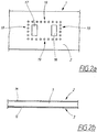
- FIG 2a and Figure 2b a respective top view and side view of a dielectric carrier material 1 used in a first embodiment example of the present invention is shown.
- the dielectric carrier material 1 has a first main side 2 and a second main side 3, originally having a metallic cladding on both sides.
- the metallic cladding is typically comprised of a layer of copper, which optionally is covered with thin layers of other metals to enhance the electrical, mechanical, and chemical properties of the cladding.
- the metallic cladding constitutes a metalization.
- the metalization on the second main side 3 is used as a ground plane G, and the metalization M on the first main side 2 is etched away to such an extent that desired metal patterns are formed on the first main side 2.
- a first surface-mounted waveguide part 4 and a second surface-mounted waveguide part 5 are mounted on the metalization M on the first main side 2.
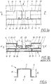
- Each waveguide part 4, 5 has three respective walls 7, 8, 9; 10, 11, 12 and one open side S (shown only in Figure 4 ), arranged to face the dielectric material 1.
- a part of the metalization M provided on the side of the dielectric carrier material 1 facing the waveguide parts 4, 5 serves as the remaining wall of the waveguide parts 4, 5, thus closing the waveguide part 4, 5 when mounted.
- a first wall 7 is arranged to be parallel to the dielectric carrier material 1 when the first waveguide part 4 is mounted, and then held at a certain distance d from said material by means of a second wall 8 and third wall 9, which second and third walls 8, 9 are arranged to contact a part of the metalization M on the first main side 2, all the walls 7, 8, 9 together essentially forming a U-shape when regarding the first waveguide part 4 from its short end.
- the second waveguide part 5 has the same configuration of its walls 10, 11, 12.
- the waveguide parts 4, 5 are mounted in a known way, each having a longitudinally extending flange part 13, 14; 15, 16 comprised in each of the second walls 8, 11 and third walls 9, 12, the flanges 13, 14; 15, 16 being arranged to be the parts of these walls 8, 11; 9, 12 which contact said part of the metalization M on the first main side 2 when the waveguide parts 4, 5 are mounted, said part of the metalization M constituting a so-called footprint.
- the flanges 13, 14; 15, 16 are soldered, or glued by means of electrically conducting glue, to the footprint on the dielectric material's first main side 2. In this particular application, there may not be any need for a particular footprint, but some kind of guidance for the mounting of the surface-mountable waveguide parts is preferred.
- the metalization M on the first main side 2 is removed such that a first aperture 17 and a second aperture 18 are formed, the apertures 17, 18 being enclosed by a frame of via holes 19.
- the via holes 19, being internally metalized, electrically connect the ground plane G with the metalization M on the first main side 2 in a known manner, forming a wall of via holes 19, enclosing the apertures 17, 18.
- the waveguide parts 4, 5 each comprise a respective first 90° bend part 20 and second 90° bend part 21 (not shown in Figure 4 ), each bend part 20, 21 having a respective first end 22 and second end 23 in the longitudinal direction of the respective waveguide part 4, 5.
- the waveguide parts 4, 5 are mounted such that the ends 22, 23 of the 90° bend parts 20, 21 face each other.
- the first 90° bend part 20 and the second 90° bend part 21 are arranged to direct a microwave signal propagating longitudinally along the respective waveguide part 4, 5 towards the dielectric carrier material 1. Then, the first 90° bend part 20 is fitted such that the first aperture 17 permits passage of a microwave signal propagating via the first 90° bend part 20. In the same way, the second 90° bend part 21 is fitted such that the second aperture 18 permits passage of a microwave signal propagating via the second 90° bend part 21.
- the dielectric carrier material 1 itself acts as a waveguide transitional part between the first aperture 17 and the second aperture 18, channeling a microwave signal. This is made possible by means of:
- the frame of via holes 19 thus forms a boundary in the dielectric carrier material 1.
- the first 90° bend part 20 and the second 90° bend part 21 each comprise a matching structure in the form of a corresponding transformer section 24, 25, as shown in Figure 3b .
- the transformer sections 24, 25 can have any suitable shape that provides sufficient matching, one such shape is shown in Figure 3b , where the height of the waveguide parts 4, 5 is decreased at the respective 90° bend part 20, 21.
- a part of the first wall 7 is arranged to be positioned closer to the dielectric carrier material 1 when the first waveguide part 4 is mounted, by decreasing the height of the second wall 8 and the third wall 9 such that said certain distance d is decreased to a lesser value d'.
- the height of the first waveguide part 4 is decreased at the first 90° bend part 20, such that the decrease of height takes place during a certain distance L from the end 22 of the first 90° bend part.
- the second waveguide part 5 has a similar configuration.
- An example of another shape of the respective transformer section is a stepped structure, having a plurality of steps.
- the shapes described are commonly known for waveguide bend parts in general.
- the metal used may be any suitable conducting material, for example copper, silver, or gold.
- the metallic claddings may be deposited onto the dielectric material by various methods, for example printing, plating, or rolling. There may also be several layers of metallic material, for example a layer comprising solder.
- the dielectric material may comprise several layers if necessary, the layers comprising different types of circuitry. Such a layered structure may also be necessary for mechanical reasons.
- the flanges may be of any suitable form, generally forming flange parts.
- the via hole frame 19 is shown as being comprised of a single row of via holes. In order to further increase leakage suppression, more than one row of via holes may be used, the frame 19 then comprising at least two adjacent rows of via holes around its circumference.
- the waveguide parts may also be made in a non-conducting material, such as plastic, which is covered by a thin layer of metalization.
Landscapes
- Engineering & Computer Science (AREA)
- Microelectronics & Electronic Packaging (AREA)
- Waveguides (AREA)
Claims (5)
- Übergangsanordnung, umfassend einen ersten oberflächenmontierbaren Wellenleiterteil (4), einen zweiten oberflächenmontierbaren Wellenleiterteil (5) und ein dielektrisches Trägermaterial (1) mit einer Metallisierung (M), die auf einer ersten Hauptseite (2) vorgesehen ist, wobei der erste oberflächenmontierbare Wellenleiterteil (4) eine erste Wand (7), eine zweite Wand (8) und eine dritte Wand (9) umfasst, wobei die zweiten und dritten Wände (8, 9) so angeordnet sind, dass sie einen Teil der Metallisierung (M) kontaktieren, alle Wände (7, 8, 9) zusammen im Wesentlichen eine U-Form bilden, der zweite oberflächenmontierbare Wellenleiterteil (5) eine erste Wand (10), eine zweite Wand (11) und eine dritte Wand (12) umfasst, wobei die zweiten und dritten Wände (11, 12) so angeordnet sind, dass sie einen Teil der Metallisierung (M) kontaktieren, alle Wände (10, 11, 12) zusammen im Wesentlichen eine U-Form bilden, das dielektrische Trägermaterial (1) ferner eine zweite Hauptseite (3) mit einer Masseebene (G) umfasst, der erste oberflächenmontierbare Wellenleiterteil (4) einen ersten gebogenen Teil (20) mit einem ersten Ende (22) umfasst, und der zweite oberflächenmontierbare Wellenleiterteil (5) außerdem einen zweiten gebogenen Teil (21) mit einem zweiten Ende (23) umfasst, wobei die Enden (22, 23) einander gegenüberliegen, wenn die oberflächenmontierbaren Wellenleiterteile (4, 5) montiert sind, wobei
die Metallisierung (M) auf der ersten Hauptseite (2) eine erste Öffnung (17) und eine zweite Öffnung (18) umfasst, die Anordnung ferner einen Rahmen von Kontaktlöchern (19) umfasst, der Rahmen von Kontaktlöchern (19) sowohl die erste als auch die zweite Öffnung (17, 18) umgibt, die Kontaktlöcher (19) die Masseebene (G) elektrisch mit der Metallisierung (M) auf der ersten Hauptseite verbinden (2), der erste gebogene Teil (20) derart installiert ist, dass die erste Öffnung (17) Durchtritt eines Mikrowellensignals ermöglicht, das sich über den ersten gebogenen Teil (20) ausbreitet, und der zweite gebogene Teil (21) derart installiert ist, dass die zweite Öffnung (18) Durchtritt eines Mikrowellensignals ermöglicht, das sich über den zweiten gebogenen Teil (21) ausbreitet, derart dass das dielektrische Trägermaterial (1) selbst als ein Wellenleiterübergang zwischen der ersten Öffnung (17) und der zweiten Öffnung (18) fungiert. - Übergangsanordnung nach Anspruch 1, dadurch gekennzeichnet, dass der erste gebogene Teil (20) und der zweite gebogene Teil (21) um 90° gebogene Teile und so angeordnet sind, dass sie ein Mikrowellensignal, das sich in Längsrichtung entlang des jeweiligen oberflächenmontierbaren Wellenleiterteils (4, 5) ausbreitet, zum dielektrischen Trägermaterial (1) leiten, wenn die oberflächenmontierbaren Wellenleiterteile (4, 5) montiert sind.
- Übergangsanordnung nach Anspruch 2, dadurch gekennzeichnet, dass der erste gebogene Teil (20) und der zweite gebogene Teil (21) jeweils eine zusammenpassende Struktur in der Form eines entsprechenden Transformatorabschnitts (24, 25) umfassen.
- Übergangsanordnung nach Anspruch 3, dadurch gekennzeichnet, dass die Transformatorabschnitte (24, 25) jeweils mindestens eine Stufe von reduzierter Höhe umfassen, wobei die jeweiligen ersten Wände (7, 10) so angeordnet sind, dass sie näher zum dielektrischen Trägermaterial (1) positioniert sind.
- Übergangsanordnung nach einem der vorhergehenden Ansprüche, dadurch gekennzeichnet, dass der Rahmen von Kontaktlöchern (19) mindestens zwei benachbarte Reihen von Kontaktlöchern um seinen Umfang umfasst.
Applications Claiming Priority (1)
| Application Number | Priority Date | Filing Date | Title |
|---|---|---|---|
| PCT/SE2008/050427 WO2009128752A1 (en) | 2008-04-16 | 2008-04-16 | A waveguide transition arrangement |
Publications (3)
| Publication Number | Publication Date |
|---|---|
| EP2277232A1 EP2277232A1 (de) | 2011-01-26 |
| EP2277232A4 EP2277232A4 (de) | 2012-04-04 |
| EP2277232B1 true EP2277232B1 (de) | 2016-06-08 |
Family
ID=41199313
Family Applications (1)
| Application Number | Title | Priority Date | Filing Date |
|---|---|---|---|
| EP08741917.2A Active EP2277232B1 (de) | 2008-04-16 | 2008-04-16 | Wellenleiterübergangsanordnung |
Country Status (3)
| Country | Link |
|---|---|
| US (1) | US8598961B2 (de) |
| EP (1) | EP2277232B1 (de) |
| WO (1) | WO2009128752A1 (de) |
Families Citing this family (12)
| Publication number | Priority date | Publication date | Assignee | Title |
|---|---|---|---|---|
| GB2489950A (en) * | 2011-04-12 | 2012-10-17 | Filtronic Plc | A substrate integrated waveguide (SIW) to air filled waveguide transition comprising a tapered dielectric layer |
| WO2013056729A1 (en) * | 2011-10-18 | 2013-04-25 | Telefonaktiebolaget L M Ericsson (Publ) | A microstrip to closed waveguide transition |
| TWI529396B (zh) * | 2014-07-18 | 2016-04-11 | Mpi Corp | Probe card and its transfer circuit board and signal feed structure |
| JP6190932B1 (ja) * | 2016-08-26 | 2017-08-30 | 株式会社フジクラ | 伝送線路 |
| JP6140872B1 (ja) * | 2016-08-26 | 2017-05-31 | 株式会社フジクラ | 伝送線路 |
| US11658378B2 (en) | 2019-10-14 | 2023-05-23 | International Business Machines Corporation | Vertically transitioning between substrate integrated waveguides (SIWs) within a multilayered printed circuit board (PCB) |
| US11399428B2 (en) | 2019-10-14 | 2022-07-26 | International Business Machines Corporation | PCB with substrate integrated waveguides using multi-band monopole antenna feeds for high speed communication |
| US11264689B2 (en) * | 2020-02-21 | 2022-03-01 | Rohde & Schwarz Gmbh & Co. Kg | Transition between a waveguide and a substrate integrated waveguide, where the transition includes a main body formed by symmetrical halves |
| CN114946082B (zh) * | 2020-03-11 | 2023-08-04 | 史莱福灵有限公司 | 带状线连接件 |
| CN115066092B (zh) * | 2021-10-09 | 2023-03-24 | 荣耀终端有限公司 | 电路板组件、制造方法及电子设备 |
| CN117477197B (zh) * | 2023-12-27 | 2024-03-26 | 成都沃特塞恩电子技术有限公司 | 波导管组件及微波设备 |
| CN118249066B (zh) * | 2024-04-17 | 2025-09-19 | 上海航天测控通信研究所 | 一种波导-微带过渡结构及其设计方法 |
Citations (1)
| Publication number | Priority date | Publication date | Assignee | Title |
|---|---|---|---|---|
| WO2001084665A1 (en) * | 2000-04-28 | 2001-11-08 | Motorola, Inc. | Filtering device and method |
Family Cites Families (11)
| Publication number | Priority date | Publication date | Assignee | Title |
|---|---|---|---|---|
| JPS6473803A (en) * | 1987-09-14 | 1989-03-20 | Fujitsu Ltd | Microwave circuit connection mechanism |
| JPH07221223A (ja) * | 1994-02-03 | 1995-08-18 | Mitsubishi Electric Corp | 半導体装置,及び混成集積回路装置 |
| US5821836A (en) * | 1997-05-23 | 1998-10-13 | The Regents Of The University Of Michigan | Miniaturized filter assembly |
| EP0959515A1 (de) | 1998-05-20 | 1999-11-24 | TRT Lucent Technologies (SA) | Verfahren zur Herstellung von Winkelstücken für Mikrowellenhohlleiter sowie nach diesem Verfahren hergestellte Winkelstücke |
| DE60208244T2 (de) * | 2001-01-12 | 2006-06-29 | Murata Manufacturing Co., Ltd., Nagaokakyo | Übertragungsleitunganordnung, integrierte Schaltung und Sender-Empfängergerät |
| JP3531624B2 (ja) * | 2001-05-28 | 2004-05-31 | 株式会社村田製作所 | 伝送線路、集積回路および送受信装置 |
| JP2003289201A (ja) * | 2002-03-28 | 2003-10-10 | Anritsu Corp | ポスト壁導波管と空洞導波管の接続変換構造 |
| DE10243671B3 (de) * | 2002-09-20 | 2004-03-25 | Eads Deutschland Gmbh | Anordnung für einen Übergang zwischen einer Mikrostreifenleitung und einem Hohlleiter |
| JP2005102024A (ja) | 2003-09-04 | 2005-04-14 | Tdk Corp | 高周波回路 |
| KR20050055204A (ko) * | 2003-12-05 | 2005-06-13 | 한국전자통신연구원 | 도파관 연결 장치 |
| FR2869725A1 (fr) | 2004-04-29 | 2005-11-04 | Thomson Licensing Sa | Element de transition sans contact entre un guide d'ondes et une ligne mocroruban |
-
2008
- 2008-04-16 US US12/988,309 patent/US8598961B2/en active Active
- 2008-04-16 EP EP08741917.2A patent/EP2277232B1/de active Active
- 2008-04-16 WO PCT/SE2008/050427 patent/WO2009128752A1/en not_active Ceased
Patent Citations (1)
| Publication number | Priority date | Publication date | Assignee | Title |
|---|---|---|---|---|
| WO2001084665A1 (en) * | 2000-04-28 | 2001-11-08 | Motorola, Inc. | Filtering device and method |
Also Published As
| Publication number | Publication date |
|---|---|
| WO2009128752A1 (en) | 2009-10-22 |
| EP2277232A1 (de) | 2011-01-26 |
| US20110037531A1 (en) | 2011-02-17 |
| EP2277232A4 (de) | 2012-04-04 |
| US8598961B2 (en) | 2013-12-03 |
Similar Documents
| Publication | Publication Date | Title |
|---|---|---|
| EP2277232B1 (de) | Wellenleiterübergangsanordnung | |
| EP2979321B1 (de) | Übergang zwischen einer siw und einer wellenleiterschnittstelle | |
| US6847274B2 (en) | Multilayer coaxial structures and resonator formed therefrom | |
| KR100282274B1 (ko) | 입체적으로 스트립선로를 사용한 전송회로 | |
| US6137064A (en) | Split via surface mount connector and related techniques | |
| US20100182105A1 (en) | Impedance-controlled coplanar waveguide system for the three-dimensional distribution of high-bandwidth signals | |
| CN100391045C (zh) | 微波传输带与波导管间的过渡装置 | |
| US7013452B2 (en) | Method and apparatus for intra-layer transitions and connector launch in multilayer circuit boards | |
| US20080314631A1 (en) | Novel via structure for improving signal integrity | |
| EP2225794B1 (de) | Wellenleiterübergangsanordnung | |
| WO2014022688A1 (en) | Multi-layer transmission lines | |
| US8227707B2 (en) | Coaxial connector mounted circuit board | |
| US20060017529A1 (en) | Multi-layer integrated RF/IF circuit board | |
| JP2009213049A (ja) | 高周波装置 | |
| US6724283B2 (en) | Arrangement mounted on a printed circuit board and method of producing such an arrangement | |
| JP2005318360A (ja) | 導波管型導波路および高周波モジュール | |
| US20060019505A1 (en) | Multi-layer integrated RF/IF circuit board | |
| WO2010130293A1 (en) | A transition from a chip to a waveguide | |
| US12548874B2 (en) | Dielectric waveguide port coupling structure including a metalized dielectric block having a blind groove with a transmission line disposed therein | |
| WO2023133750A1 (en) | Ultra wideband board-to-board transitions for stripline rf transmisison lines | |
| JP2009303076A (ja) | 導波管の接続構造 | |
| US20210135329A1 (en) | Implementation of inductive posts in an siw structure and production of a generic filter | |
| US12362489B2 (en) | Very efficient 5G/6G antenna array system (AAS) feed | |
| EP2215684B1 (de) | Übergangsanordnung von mikrostreifen zu wellenleiter | |
| WO2009127253A1 (en) | A waveguide filter arrangement |
Legal Events
| Date | Code | Title | Description |
|---|---|---|---|
| PUAI | Public reference made under article 153(3) epc to a published international application that has entered the european phase |
Free format text: ORIGINAL CODE: 0009012 |
|
| 17P | Request for examination filed |
Effective date: 20101112 |
|
| AK | Designated contracting states |
Kind code of ref document: A1 Designated state(s): AT BE BG CH CY CZ DE DK EE ES FI FR GB GR HR HU IE IS IT LI LT LU LV MC MT NL NO PL PT RO SE SI SK TR |
|
| AX | Request for extension of the european patent |
Extension state: AL BA MK RS |
|
| DAX | Request for extension of the european patent (deleted) | ||
| A4 | Supplementary search report drawn up and despatched |
Effective date: 20120306 |
|
| RIC1 | Information provided on ipc code assigned before grant |
Ipc: H05K 1/02 20060101ALI20120229BHEP Ipc: H01P 5/08 20060101AFI20120229BHEP Ipc: H05K 1/18 20060101ALI20120229BHEP Ipc: H01P 5/02 20060101ALI20120229BHEP Ipc: H01P 1/02 20060101ALI20120229BHEP |
|
| 17Q | First examination report despatched |
Effective date: 20130726 |
|
| GRAP | Despatch of communication of intention to grant a patent |
Free format text: ORIGINAL CODE: EPIDOSNIGR1 |
|
| INTG | Intention to grant announced |
Effective date: 20151223 |
|
| GRAS | Grant fee paid |
Free format text: ORIGINAL CODE: EPIDOSNIGR3 |
|
| GRAA | (expected) grant |
Free format text: ORIGINAL CODE: 0009210 |
|
| AK | Designated contracting states |
Kind code of ref document: B1 Designated state(s): AT BE BG CH CY CZ DE DK EE ES FI FR GB GR HR HU IE IS IT LI LT LU LV MC MT NL NO PL PT RO SE SI SK TR |
|
| REG | Reference to a national code |
Ref country code: GB Ref legal event code: FG4D |
|
| REG | Reference to a national code |
Ref country code: CH Ref legal event code: EP |
|
| REG | Reference to a national code |
Ref country code: IE Ref legal event code: FG4D |
|
| REG | Reference to a national code |
Ref country code: AT Ref legal event code: REF Ref document number: 805804 Country of ref document: AT Kind code of ref document: T Effective date: 20160715 |
|
| REG | Reference to a national code |
Ref country code: DE Ref legal event code: R096 Ref document number: 602008044613 Country of ref document: DE |
|
| REG | Reference to a national code |
Ref country code: LT Ref legal event code: MG4D |
|
| REG | Reference to a national code |
Ref country code: NL Ref legal event code: MP Effective date: 20160608 |
|
| PG25 | Lapsed in a contracting state [announced via postgrant information from national office to epo] |
Ref country code: FI Free format text: LAPSE BECAUSE OF FAILURE TO SUBMIT A TRANSLATION OF THE DESCRIPTION OR TO PAY THE FEE WITHIN THE PRESCRIBED TIME-LIMIT Effective date: 20160608 Ref country code: NO Free format text: LAPSE BECAUSE OF FAILURE TO SUBMIT A TRANSLATION OF THE DESCRIPTION OR TO PAY THE FEE WITHIN THE PRESCRIBED TIME-LIMIT Effective date: 20160908 Ref country code: LT Free format text: LAPSE BECAUSE OF FAILURE TO SUBMIT A TRANSLATION OF THE DESCRIPTION OR TO PAY THE FEE WITHIN THE PRESCRIBED TIME-LIMIT Effective date: 20160608 |
|
| REG | Reference to a national code |
Ref country code: AT Ref legal event code: MK05 Ref document number: 805804 Country of ref document: AT Kind code of ref document: T Effective date: 20160608 |
|
| PG25 | Lapsed in a contracting state [announced via postgrant information from national office to epo] |
Ref country code: ES Free format text: LAPSE BECAUSE OF FAILURE TO SUBMIT A TRANSLATION OF THE DESCRIPTION OR TO PAY THE FEE WITHIN THE PRESCRIBED TIME-LIMIT Effective date: 20160608 Ref country code: GR Free format text: LAPSE BECAUSE OF FAILURE TO SUBMIT A TRANSLATION OF THE DESCRIPTION OR TO PAY THE FEE WITHIN THE PRESCRIBED TIME-LIMIT Effective date: 20160909 Ref country code: NL Free format text: LAPSE BECAUSE OF FAILURE TO SUBMIT A TRANSLATION OF THE DESCRIPTION OR TO PAY THE FEE WITHIN THE PRESCRIBED TIME-LIMIT Effective date: 20160608 Ref country code: SE Free format text: LAPSE BECAUSE OF FAILURE TO SUBMIT A TRANSLATION OF THE DESCRIPTION OR TO PAY THE FEE WITHIN THE PRESCRIBED TIME-LIMIT Effective date: 20160608 Ref country code: LV Free format text: LAPSE BECAUSE OF FAILURE TO SUBMIT A TRANSLATION OF THE DESCRIPTION OR TO PAY THE FEE WITHIN THE PRESCRIBED TIME-LIMIT Effective date: 20160608 Ref country code: HR Free format text: LAPSE BECAUSE OF FAILURE TO SUBMIT A TRANSLATION OF THE DESCRIPTION OR TO PAY THE FEE WITHIN THE PRESCRIBED TIME-LIMIT Effective date: 20160608 |
|
| PG25 | Lapsed in a contracting state [announced via postgrant information from national office to epo] |
Ref country code: CZ Free format text: LAPSE BECAUSE OF FAILURE TO SUBMIT A TRANSLATION OF THE DESCRIPTION OR TO PAY THE FEE WITHIN THE PRESCRIBED TIME-LIMIT Effective date: 20160608 Ref country code: IS Free format text: LAPSE BECAUSE OF FAILURE TO SUBMIT A TRANSLATION OF THE DESCRIPTION OR TO PAY THE FEE WITHIN THE PRESCRIBED TIME-LIMIT Effective date: 20161008 Ref country code: RO Free format text: LAPSE BECAUSE OF FAILURE TO SUBMIT A TRANSLATION OF THE DESCRIPTION OR TO PAY THE FEE WITHIN THE PRESCRIBED TIME-LIMIT Effective date: 20160608 Ref country code: IT Free format text: LAPSE BECAUSE OF FAILURE TO SUBMIT A TRANSLATION OF THE DESCRIPTION OR TO PAY THE FEE WITHIN THE PRESCRIBED TIME-LIMIT Effective date: 20160608 Ref country code: EE Free format text: LAPSE BECAUSE OF FAILURE TO SUBMIT A TRANSLATION OF THE DESCRIPTION OR TO PAY THE FEE WITHIN THE PRESCRIBED TIME-LIMIT Effective date: 20160608 Ref country code: SK Free format text: LAPSE BECAUSE OF FAILURE TO SUBMIT A TRANSLATION OF THE DESCRIPTION OR TO PAY THE FEE WITHIN THE PRESCRIBED TIME-LIMIT Effective date: 20160608 |
|
| PG25 | Lapsed in a contracting state [announced via postgrant information from national office to epo] |
Ref country code: AT Free format text: LAPSE BECAUSE OF FAILURE TO SUBMIT A TRANSLATION OF THE DESCRIPTION OR TO PAY THE FEE WITHIN THE PRESCRIBED TIME-LIMIT Effective date: 20160608 Ref country code: BE Free format text: LAPSE BECAUSE OF FAILURE TO SUBMIT A TRANSLATION OF THE DESCRIPTION OR TO PAY THE FEE WITHIN THE PRESCRIBED TIME-LIMIT Effective date: 20160608 Ref country code: PT Free format text: LAPSE BECAUSE OF FAILURE TO SUBMIT A TRANSLATION OF THE DESCRIPTION OR TO PAY THE FEE WITHIN THE PRESCRIBED TIME-LIMIT Effective date: 20161010 Ref country code: PL Free format text: LAPSE BECAUSE OF FAILURE TO SUBMIT A TRANSLATION OF THE DESCRIPTION OR TO PAY THE FEE WITHIN THE PRESCRIBED TIME-LIMIT Effective date: 20160608 |
|
| REG | Reference to a national code |
Ref country code: DE Ref legal event code: R097 Ref document number: 602008044613 Country of ref document: DE |
|
| PLBE | No opposition filed within time limit |
Free format text: ORIGINAL CODE: 0009261 |
|
| STAA | Information on the status of an ep patent application or granted ep patent |
Free format text: STATUS: NO OPPOSITION FILED WITHIN TIME LIMIT |
|
| 26N | No opposition filed |
Effective date: 20170309 |
|
| PG25 | Lapsed in a contracting state [announced via postgrant information from national office to epo] |
Ref country code: DK Free format text: LAPSE BECAUSE OF FAILURE TO SUBMIT A TRANSLATION OF THE DESCRIPTION OR TO PAY THE FEE WITHIN THE PRESCRIBED TIME-LIMIT Effective date: 20160608 Ref country code: SI Free format text: LAPSE BECAUSE OF FAILURE TO SUBMIT A TRANSLATION OF THE DESCRIPTION OR TO PAY THE FEE WITHIN THE PRESCRIBED TIME-LIMIT Effective date: 20160608 |
|
| REG | Reference to a national code |
Ref country code: DE Ref legal event code: R119 Ref document number: 602008044613 Country of ref document: DE |
|
| REG | Reference to a national code |
Ref country code: CH Ref legal event code: PL |
|
| REG | Reference to a national code |
Ref country code: IE Ref legal event code: MM4A |
|
| REG | Reference to a national code |
Ref country code: FR Ref legal event code: ST Effective date: 20171229 |
|
| PG25 | Lapsed in a contracting state [announced via postgrant information from national office to epo] |
Ref country code: MC Free format text: LAPSE BECAUSE OF FAILURE TO SUBMIT A TRANSLATION OF THE DESCRIPTION OR TO PAY THE FEE WITHIN THE PRESCRIBED TIME-LIMIT Effective date: 20160608 Ref country code: DE Free format text: LAPSE BECAUSE OF NON-PAYMENT OF DUE FEES Effective date: 20171103 Ref country code: FR Free format text: LAPSE BECAUSE OF NON-PAYMENT OF DUE FEES Effective date: 20170502 |
|
| PG25 | Lapsed in a contracting state [announced via postgrant information from national office to epo] |
Ref country code: LI Free format text: LAPSE BECAUSE OF NON-PAYMENT OF DUE FEES Effective date: 20170430 Ref country code: LU Free format text: LAPSE BECAUSE OF NON-PAYMENT OF DUE FEES Effective date: 20170416 Ref country code: CH Free format text: LAPSE BECAUSE OF NON-PAYMENT OF DUE FEES Effective date: 20170430 |
|
| PG25 | Lapsed in a contracting state [announced via postgrant information from national office to epo] |
Ref country code: IE Free format text: LAPSE BECAUSE OF NON-PAYMENT OF DUE FEES Effective date: 20170416 |
|
| PG25 | Lapsed in a contracting state [announced via postgrant information from national office to epo] |
Ref country code: MT Free format text: LAPSE BECAUSE OF NON-PAYMENT OF DUE FEES Effective date: 20170416 |
|
| PG25 | Lapsed in a contracting state [announced via postgrant information from national office to epo] |
Ref country code: HU Free format text: LAPSE BECAUSE OF FAILURE TO SUBMIT A TRANSLATION OF THE DESCRIPTION OR TO PAY THE FEE WITHIN THE PRESCRIBED TIME-LIMIT; INVALID AB INITIO Effective date: 20080416 |
|
| PG25 | Lapsed in a contracting state [announced via postgrant information from national office to epo] |
Ref country code: BG Free format text: LAPSE BECAUSE OF FAILURE TO SUBMIT A TRANSLATION OF THE DESCRIPTION OR TO PAY THE FEE WITHIN THE PRESCRIBED TIME-LIMIT Effective date: 20160608 |
|
| PG25 | Lapsed in a contracting state [announced via postgrant information from national office to epo] |
Ref country code: CY Free format text: LAPSE BECAUSE OF NON-PAYMENT OF DUE FEES Effective date: 20160608 |
|
| PG25 | Lapsed in a contracting state [announced via postgrant information from national office to epo] |
Ref country code: TR Free format text: LAPSE BECAUSE OF FAILURE TO SUBMIT A TRANSLATION OF THE DESCRIPTION OR TO PAY THE FEE WITHIN THE PRESCRIBED TIME-LIMIT Effective date: 20160608 |
|
| PGFP | Annual fee paid to national office [announced via postgrant information from national office to epo] |
Ref country code: GB Payment date: 20250428 Year of fee payment: 18 |