EP2272087B1 - Method for providing oxide layers - Google Patents
Method for providing oxide layers Download PDFInfo
- Publication number
- EP2272087B1 EP2272087B1 EP09738240.2A EP09738240A EP2272087B1 EP 2272087 B1 EP2272087 B1 EP 2272087B1 EP 09738240 A EP09738240 A EP 09738240A EP 2272087 B1 EP2272087 B1 EP 2272087B1
- Authority
- EP
- European Patent Office
- Prior art keywords
- substrate
- oxide layer
- electrolyte solution
- potential
- oxide
- Prior art date
- Legal status (The legal status is an assumption and is not a legal conclusion. Google has not performed a legal analysis and makes no representation as to the accuracy of the status listed.)
- Not-in-force
Links
Images


Classifications
-
- H—ELECTRICITY
- H10—SEMICONDUCTOR DEVICES; ELECTRIC SOLID-STATE DEVICES NOT OTHERWISE PROVIDED FOR
- H10P—GENERIC PROCESSES OR APPARATUS FOR THE MANUFACTURE OR TREATMENT OF DEVICES COVERED BY CLASS H10
- H10P14/00—Formation of materials, e.g. in the shape of layers or pillars
- H10P14/60—Formation of materials, e.g. in the shape of layers or pillars of insulating materials
- H10P14/63—Formation of materials, e.g. in the shape of layers or pillars of insulating materials characterised by the formation processes
- H10P14/6302—Non-deposition formation processes
- H10P14/6324—Formation by anodic treatments, e.g. anodic oxidation
-
- H—ELECTRICITY
- H10—SEMICONDUCTOR DEVICES; ELECTRIC SOLID-STATE DEVICES NOT OTHERWISE PROVIDED FOR
- H10P—GENERIC PROCESSES OR APPARATUS FOR THE MANUFACTURE OR TREATMENT OF DEVICES COVERED BY CLASS H10
- H10P14/00—Formation of materials, e.g. in the shape of layers or pillars
- H10P14/60—Formation of materials, e.g. in the shape of layers or pillars of insulating materials
- H10P14/63—Formation of materials, e.g. in the shape of layers or pillars of insulating materials characterised by the formation processes
- H10P14/6302—Non-deposition formation processes
- H10P14/6304—Formation by oxidation, e.g. oxidation of the substrate
- H10P14/6306—Formation by oxidation, e.g. oxidation of the substrate of the semiconductor materials
- H10P14/6308—Formation by oxidation, e.g. oxidation of the substrate of the semiconductor materials of Group IV semiconductors
- H10P14/6309—Formation by oxidation, e.g. oxidation of the substrate of the semiconductor materials of Group IV semiconductors of silicon in uncombined form, i.e. pure silicon
Definitions
- the present invention relates to semiconductor processing. More particularly, the present invention relates to a method for providing an oxide layer at predetermined locations on a substrate, e.g. on a three-dimensional structure in a substrate, for example a three-dimensional structure having a high aspect ratio, for example an aspect ratio (width over height ratio) below 5.
- Silicon oxide is a know material to be used in semiconductor process technology. Several techniques exist to deposit or grow silicon oxide. Silicon oxide may be formed by thermal oxidation of silicon. Alternatively, Chemical Vapour deposition (CVD) may be used to form silicon oxide. By using this process, silicon oxide is formed by a chemical reaction in a process chamber at temperatures typically ranging from 200°C to 500°C. For this purpose specific precursors such as e.g. silane (SiH 4 ), TEOS (Tetraethyl Orthosilicate - Si(OC 2 H 5 ) 4 ) or HMDSO (hexamethyldisiloxane) are commonly used.
- silane SiH 4
- TEOS Tetraethyl Orthosilicate - Si(OC 2 H 5 ) 4
- HMDSO hexamethyldisiloxane
- the quality (electrical and mechanical properties) of the formed oxide mainly depends on the amount of impurities trapped in the oxide during formation, and thus also depends on the technique used to form it.
- the impurities may, for example, result from incompletely dissociated precursors.
- PECVD Plasma Enhanced Chemical Vapour Deposition
- silicon oxide is by electrochemical oxidation of silicon, such as anodisation.
- US 5,736,454 describes a method for forming a silicon dioxide layer on a silicon substrate, e.g. a field oxide layer or the oxide layer of a thin film transistor.
- the method comprises conducting an electrolytic reaction at room temperature such that a silicon dioxide layer is formed on a silicon substrate acting as an anode, wherein pure water is used as an electrolyte of the electrolytic reaction.
- an aluminium film is evaporated at the backside of the silicon substrate to form the anodic contact for anodisation.
- the method of US 5,736,454 requires assist techniques in order to obtain good quality silicon oxide that can be used as, for example, a gate oxide.
- the formed silicon dioxide layer is further subjected to a rapid thermal densification carried out in an inert gas atmosphere and at a temperature of between 700°C and 1000°C for a time period such that the silicon dioxide is densified.
- a rapid thermal densification carried out in an inert gas atmosphere and at a temperature of between 700°C and 1000°C for a time period such that the silicon dioxide is densified.
- PECVD deposition is typically performed at temperatures between 200°C and 400°C.
- typical deposition temperatures need to remain below 200°, preferably below 100°C for example to allow processing on carrier wafers, that are typically glued with polymer based materials that cannot withstand these high temperatures.
- PECVD it is possible to deposit layers at temperatures below 200°C, often down to 80°C, but the oxide deposited at these temperatures exhibit poor properties, for example poor mechanical properties.
- the layers suffer from low breakdown field and pinholes.
- the conformity of the deposited layers is poor, i.e. the thickness of the deposited layer is not homogenous in deep 3D structures.
- DE 101 38 981 A1 A method for forming silicon oxide films by electrochemical oxidation of silicon substrates is described in DE 101 38 981 A1 (INFINEON TECHNOLOGIES AG [DE]) 6 March 2003 (2003-03-06).
- the oxides taught by DE 101 38 981 A1 are formed on substrates having deep 3D structures.
- Oxidation of silicon appears to be a difficult process that may require posttreatment, additional assist techniques or specific substrate preparation in order to form good quality oxide.
- a good quality oxide for example has a parasitic leakage current below 100nA/cm 2 .
- a method for providing an oxide layer on a semiconductor substrate for example on a three-dimensional (3D) structure on or in a semiconductor substrate, for example a silicon substrate.
- oxide layers may be formed on a 3D structure in or on a semiconductor substrate, e.g. at the sidewalls of trenches or holes in and/or at the sidewalls of pillars at a major surface of a semiconductor substrate.
- a method according to embodiments of the invention may be applied at low temperatures, e.g. temperatures below 80°C, for example room temperature.
- the present invention provides a method for providing an oxide layer on a semiconductor substrate, for example on a three-dimensional structure in or on a semiconductor substrate.
- the method comprises:
- the substrate comprises a three-dimensional structure
- such three-dimensional structure could, as examples only, be a cylindrical or donut-shaped hole for a through-substrate via (TSV). In alternative embodiments it could be any shape structured on the surface of the substrate, e.g. for forming a MEMS device.
- the three-dimensional structures include trenches, holes and/or pillars.
- Anodising the substrate in an acidic electrolyte solution may comprise immersing the substrate in an electrolyte solution which comprises any of citric acid, acetic acid, oxalic acid, sulfuric acid, phosphoric acid nitric acid or a combination thereof.
- the concentration of the acid in the electrolyte solution may be between 0% (not included) and 20%, depending on the acid used and on particular circumstances.
- oxide layers may be formed at predetermined locations, e.g. those locations where substrate is exposed to the electrolyte.
- predetermined locations may include parts of a three-dimensional structure, for example on a major surface of the three-dimensional structure and/or at sidewalls thereof, for example sidewalls of a trench or hole or via.
- An advantage of the use of anodisation is the realisation of a uniform oxide thickness on the substrate surface exposed to the anodisation electrolyte and the simultaneous reduction of the surface roughness.
- Etching of vertical trenches or vias in a substrate typically results in rough sidewalls (Scallops).
- Sharp surface features on the substrate-surfaces e.g. the scallops
- a smooth surface, or thus reduced roughness, of the oxide provides good electrical properties, such as for example improved resistance against breakdown.
- Another advantage of a method according to embodiments of the invention is that it can be applied at low temperatures, e.g. below 80°C, even below 50°C, such as at room temperature.
- a method according to embodiments of the invention may be used for forming vias, e.g. through-substrate vias, or MEMS devices.
- the oxide layer formed may be provided at the front side of the substrate.
- Applying a potential between a cathode and an anode may comprise applying a potential between a cathode and an anode located at the front side of the substrate.
- This has the advantage that the method may also be used with very thin substrates. Such thin substrates are, for convenience of handling, placed on a handling wafer. Such handling wafer is most often non-conductive. Due to the provision of a potential between the cathode and an anode at the front side of the substrate, the presence and type of handling wafer is of no concern for the anodisation process.
- the applied potential may be between 10 V and 400V.
- the current should be high enough to start electrolysis of the electrolyte solution.
- applying a potential between a cathode located in the electrolyte solution and an anode formed on or by the substrate may be performed by applying a potential so as to change current density through the substrate as a function of time.
- the applied potential may change as a function of time.
- anodisation may be performed by a two-step process.
- applying a potential between a cathode located in the electrolyte solution and an anode formed on or by the substrate may be performed such that:
- healing of the oxide layer is meant removal of defects such as pinholes so as to obtain an oxide layer of good quality.
- the present invention provides the use of a method according to embodiments of the present invention in a manufacturing process for semiconductor devices.
- the present invention provides a substrate provided with an oxide layer, wherein the oxide layer is formed by a method according to embodiments of the present invention.
- the present invention provides a three-dimensional structure on a substrate, the three-dimensional structure comprising at least one hole.
- the three-dimensional structure furthermore comprises an oxide layer on a major surface of the three-dimensional structure and/or at sidewalls of the at least one hole, the oxide layer being formed by a method according to embodiments of the present invention. It is particularly advantageous that the formed oxide layer is conformal in high aspect ratio three-dimensional structures, e.g. trenches.
- Known low temperature processes typically have less than 10% step-coverage whereas an oxide layer formed in accordance with embodiments of the present invention is conformal like a CVD oxide, but contrary thereto is provided at low temperature.
- the present invention relates to the field of semiconductor processing, e.g. silicon processing, for example through-substrate via processing and semiconductor based MEMS technology.
- the semiconductor may be silicon.
- the present invention is described in detail with reference to a substrate provided with a three-dimensional structure, which is the examples described is a hole. This, however, is not intended to be limiting for the present invention.
- the invention can also be applied to substrates with three-dimensional structures which are pillars or which have a pillar-like shape, to substrates provided with other types of three-dimensional structures, or to plane substrates.
- the present invention provides a method for providing an oxide layer on exposed semiconductor surface areas of a three-dimensional semiconductor, e.g. silicon, structure. The method comprises:
- Anodisation is an electrochemical process in which a surface is anodised by placing the surface into an electrolyte solution while applying a potential between a cathode (negative electrode) formed of an inert material and an anode (positive electrode).
- the anode can be the part to be treated or can be additionally provided onto the part to be treated.
- An oxide layer is then grown because of a direct current passing through the electrolyte solution as a consequence of the applied potential. This current releases hydrogen at the cathode and oxygen at a surface of the anode, thereby creating a build-up of the oxide layer.
- Anodisation allows growing oxides at room temperature.
- oxide layers may be provided in holes or on protrusions of a three-dimensional (3D) structure. Therefore, by using anodisation to provide an oxide layer in holes or on protrusions of the 3D structure, a method according to embodiments of the invention may overcome limitations of prior art processes such as chemical vapour deposition (CVD) techniques, and allows for process simplifications, and thus consequently for cost reduction.
- CVD chemical vapour deposition
- the anodisation process is carried out in an acidic electrolyte solution.
- the electrolyte solution may, for example, comprise any of citric acid, acetic acid, oxalic acid, sulfuric acid, phosphoric acid nitric acid or a combination thereof. It has been found that the acid component in the electrolyte solution speeds up the anodisation process. Therefore, by using an acidic electrolyte solution, a thicker oxide can be grown in a particular time compared to an anodisation process with same parameters (starting materials, current, temperature etc.) but using another, non-acidic, electrolyte solution. The more acidic the electrolyte solution, the faster the anodisation process takes place.
- Anodisation results in the realisation of a uniform oxide thickness on the semiconductor, e.g. Si, surfaces exposed to the anodisation electrolyte.
- the thickness of the oxide layer is defined by the anodisation voltage between the cathode and the anode, which defines the anodisation current.
- Anodisation also results in the simultaneous reduction of the surface roughness.
- Etching of vertical trenches or vias in semiconductor material, for example in Si typically results in rough sidewalls (Scallops).
- Sharp surface features on the semiconductor surfaces, e.g. Si-surfaces, (e.g. the scallops) result locally in higher electro-static fields, accelerating the anodic oxidation process at those locations and therefore smoothening the surface in a natural way.
- Embodiments of the present invention propose to use an anodisation process to provide oxide layers on or in a three-dimensional (3D) structure formed on or in a semiconductor substrate.
- the method according to embodiments of the invention may be used for providing oxide layers in any 3D structure on a substrate, as long as the substrate and/or 3D structure comprise a conductive material such as a metal or a semiconductor material.
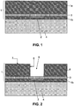
- a device substrate 1a for example a Si substrate, is provided.
- a dielectric insulating layer 3 such as an oxide or a nitride is provided.
- the dielectric insulating layer 3 may consist of a single layer or a plurality of layers.
- active device such as for example transistors (not illustrated) may be provided in the device substrate 1a, e.g. the front end of line.
- the device substrate 1a could be a passive substrate.
- a multilayer interconnect structure 1b is provided, comprising insulating and interconnect layers, e.g.
- FIG. 1 schematically illustrated and indicated by reference number 2.
- the substrate 1 formed by the plurality of layers and devices as mentioned above may optionally be attached to a carrier substrate 4.
- the substrate 1 may have a thickness of smaller than 300 ⁇ m, and may, for example, have a thickness of between 50 ⁇ m and 300 ⁇ m.
- any substrate may be used as long as it can conduct an electrical current and can be oxidised, such as e.g. a semiconductor substrate, in particular a silicon substrate.
- the substrate 1, and more particularly device substrate 1a thereof, which is the part which will be anodised may comprise low resistivity silicon.
- the low resistivity silicon may have a resistivity of 30 ⁇ Ohm.cm or lower, the invention however not being limited thereto.
- n- or p-doped semiconductor material such as n- or p-doped silicon may be used.
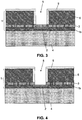
- holes 5 may be etched from the backside of the semiconductor device wafer 1a to the insulating layer 3.
- a typical technique would be to use an ICP-RIE plasma etching technique to obtain sloped or straight sidewalls 8.
- These holes 5 may have a variety of shapes: circular, polygons, ring shapes or trenches to name only a few.
- the substrate 1 may be immersed in an acidic electrolyte solution, and a potential may be applied between a cathode located in the electrolyte solution and an anode formed on or by the substrate1.
- the applied potential may be between 10 V and 400 V.
- the material of the substrate 1, in particular the device substrate1a itself may act as an anode.
- an anode may be formed on the substrate 1 such that it makes electrical contact to the conductive material of the substrate 1. In the latter case, a contact ohmic resistance of between 10 k ⁇ and 100 k ⁇ may exist between the electrode and the substrate 1.
- This contact may be realised with a distributed set of electrodes embedded in a plastic mould able to protect the contact from the acid solution.
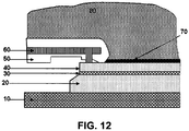
- An example of such electrode is illustrated in FIG. 12 .
- the electrode 60 illustrated in FIG. 12 may be only one of a plurality of distributed electrodes.
- the electrode 60 is covered by a contact seal ring 50 which prevents direct contact between the electrode 60 and the surrounding electrolyte solution 80, so that the electrode 60 cannot be contaminated or destroyed by the acidic electrolyte solution.
- the contact seal ring 50 is of a material suitable for protecting the electrode 60 against the acidic impact of the electrolyte solution.
- the electrode 60 is in electrical contact with the substrate 40, for example a thin semiconductor wafer, at the front side thereof, i.e.
- the substrate 40 to be oxidised may be attached onto a carrier wafer 20, for example by means of a temporary glue 30.
- the substrate 40 optionally provided onto and temporarily attached to the carrier wafer 20, may be placed onto a holder chuck 10.
- the device substrate 1a itself as a distributed electrode. This way, no anode needs to be provided at the back of the substrate 1, which in the example illustrated would be at the back of the carrier substrate 4.
- the electrolyte solution may, for example, comprise citric acid, acetic acid, oxalic acid, sulfuric acid, phosphoric acid nitric acid or a combination thereof.
- a voltage By applying a voltage to the substrate 1, a current will pass through the electrolyte solution thereby causing anodisation of conductive material in contact with the electrolyte solution.
- a silicon oxide layer 9 is formed on all exposed silicon surfaces, e.g. the major surface 7 as well as the side walls 8 of the 3D structure, ( FIG. 3 ).
- the anodisation process is selective towards the insulator 3. This means that the oxide will only be formed at exposed conductive substrate material, substantially not on neighbouring non-conductive or non-conducting materials.
- an oxide layer 9, e.g. silicon oxide layer on the major surface 7 and side walls 8 is only an example and that, according to other embodiments of the invention, the method also may be used to, for example, provide an oxide layer 9, e.g. silicon oxide layer, only at the side walls 8 of the at least one hole 5. This may be performed by, for example, first providing an insulating layer to the major surface 7 of the 3D structure and then anodising the non-covered parts, i.e. the side walls 8 of the at least one hole 5 so as to form the oxide layer 9, e.g. silicon oxide layer on the side walls 8 of the at least one hole 5.
- Anodisation is a self limiting process, which means that there exists an equilibrium between the potential that is applied for anodisation and the resulting thickness of the oxide layer 9 formed. According to embodiments of the invention it may be possible to form oxide layers 9 with a thickness up to 200 nm. According to embodiments and depending on the required thickness of the oxide layer 9, e.g. silicon oxide layer, anodisation may be performed during a time period between about 10 min and 10 hours.
- the anodisation process may be a two-step process.
- a potential may be applied between the cathode and anode such that a fixed current density is obtained which allows forming of the oxide layer 9.
- the applied potential may be a fixed potential which allows healing the formed oxide layer 9, e.g. silicon oxide layer.
- healing of the oxide layer 9, e.g. silicon oxide layer is meant removal of defects such as pinholes so as to obtain an oxide layer of good quality.
- a stoichiometric oxide may be obtained, which exhibits good quality features.
- porous oxide layers 9 e.g. silicon oxide layers.
- the current density may be changed as a function of time during anodisation.
- the insulating layer 3 at the bottom of the at least one hole 5 may be removed so as to expose the contacts 2 underneath. This may be done by any suitable technique known by a person skilled in the art, for example by selective etching. In this case the insulating layer 3 should preferably be selectively etchable with respect to the formed oxide layer 9. The at least one hole or via 5 may then optionally be filled with a conductive material.
- a method according to embodiments of the invention may be used in semiconductor processing.
- a method according to embodiments of the invention may be used to form a liner of a through-silicon-via, also referred to as via isolation.
- the oxide layer 9, e.g. silicon oxide layer occurs at predetermined locations, in the example given on the major surface 7 of the 3D structure and on the sidewalls 8 of the at least one hole or via 5
- no patterning step is required to pattern the formed oxide layer 9, in the example given silicon oxide layer, so as to remove the part of the oxide layer 9, in the example given silicon oxide layer from the bottom of the at least one hole or via 5.
- a method according to embodiments of the invention may be used for providing oxide layers 9, e.g. silicon oxide layers, in vias 5 with high aspect ratio, which may be defined as the width-to-height ratio, e.g. with an aspect ratio below 5, for example an aspect ratio of between 0.01 and 5.
- high aspect ratio which may be defined as the width-to-height ratio, e.g. with an aspect ratio below 5, for example an aspect ratio of between 0.01 and 5.
- the oxide layer 9, e.g. silicon oxide layer formed by a method according to embodiments of the invention has a normal stoichiometry, i.e. has a same stoichiometry as oxide layers formed by conventional methods.
- the oxide layer 9, e.g. silicon oxide layer formed by a method according to embodiments of the present invention exhibits minimum quality that may be required for 3D integration.
- the oxide layers 9, e.g. silicon oxide layer formed by a method according to embodiments are less suitable for being used as a gate oxide.
- a surface when a Si surface is treated with the method according to embodiments of the invention, i.e. when a silicon oxide layer is formed using a method according to embodiments of the invention, a surface may be obtained with hydrophilic properties. These properties may be used in order to ease the application of lithographic products on the wafer surface.
- oxide layers e.g. silicon oxide layers may be formed on a 3D structure on a semiconductor substrate, e.g. at sidewalls of trenches or holes or vias 5 in and/or at a major surface of a three-dimensional structure.
- a method according to embodiments of the present invention does not always require additional steps, such as e.g. photolithography steps, for patterning the formed oxide layer, thereby removing the oxide at locations where no oxide is wanted.
- a method according to embodiments of the invention may be applied at room temperature, thereby avoiding problems that can arise with, for example, glue layers, during heating.
- continuous and conformal oxide layers may be obtained.
- a silicon oxide layer 9 was provided into a silicon hole or via 5. Therefore a silicon wafer 1 was provided.
- the silicon wafer 1 was provided with through-silicon-vias 5 having a high aspect ratio of 0.1 (diameter of 5 ⁇ m and depth of 50 ⁇ m).
- the silicon wafer 1 was cleaned with a HF solution in order to ensure low contact resistance.
- an electrolyte solution for the anodisation reaction a 0.1% citric acid solution was used. An anodisation potential of 40 V was applied. A current density of 5 mA/cm 2 was achieved. Anodisation was performed during a time period of 10 hours. A silicon oxide layer 9 with a thickness of 70nm was obtained.
- FIG. 6 to FIG. 11 show pictures of the resulting oxide layer in the hole 5.
- the oxide layer had a thickness of 70nm.
- FIG. 7 shows the detail indicated A in FIG. 6 .
- FIG. 8 shows the detail indicated B in FIG. 6 .
- FIG. 9 shows the bottom of the hole 5.
- FIG. 10 shows the detail indicated C in FIG. 9 .
- FIG. 11 shows the detail indicated D in FIG. 9 .
- part 1a of the substrate 1 may comprise isolation zones such as STI zones which are well known by a person skilled in the art.
- Part 1b of the substrate 1 may comprise a plurality of vias via1, ..., via n and a plurality of metal layers M1, ..., Mn+1 to form contacts 2.
- an insulating layer 3 is present.
- the insulating layer 3 may be formed of a first layer 3a and a second layer 3b.
- the first layer 3a may, for example, comprise HDPO (high density plasma oxide) with a thickness of, for example, in the example illustrated, 400 nm.
- the second layer 3b may, for example, comprise SiC with a thickness of, for example, in the example illustrated, 50 nm.
- the SiC layer 3b acts as an etch stop when etching the at least one hole or via 5 in part 1a of the substrate 1.
- An oxide layer can be applied in the hole or via 5 as in accordance with embodiments of the present invention.
Landscapes
- Internal Circuitry In Semiconductor Integrated Circuit Devices (AREA)
- Formation Of Insulating Films (AREA)
Applications Claiming Priority (2)
| Application Number | Priority Date | Filing Date | Title |
|---|---|---|---|
| US5009208P | 2008-05-02 | 2008-05-02 | |
| PCT/EP2009/055312 WO2009133196A1 (en) | 2008-05-02 | 2009-04-30 | Method for providing oxide layers |
Publications (2)
| Publication Number | Publication Date |
|---|---|
| EP2272087A1 EP2272087A1 (en) | 2011-01-12 |
| EP2272087B1 true EP2272087B1 (en) | 2018-04-04 |
Family
ID=40941299
Family Applications (1)
| Application Number | Title | Priority Date | Filing Date |
|---|---|---|---|
| EP09738240.2A Not-in-force EP2272087B1 (en) | 2008-05-02 | 2009-04-30 | Method for providing oxide layers |
Country Status (4)
| Country | Link |
|---|---|
| US (1) | US8822330B2 (cg-RX-API-DMAC7.html) |
| EP (1) | EP2272087B1 (cg-RX-API-DMAC7.html) |
| JP (1) | JP5528430B2 (cg-RX-API-DMAC7.html) |
| WO (1) | WO2009133196A1 (cg-RX-API-DMAC7.html) |
Families Citing this family (3)
| Publication number | Priority date | Publication date | Assignee | Title |
|---|---|---|---|---|
| US8912522B2 (en) * | 2009-08-26 | 2014-12-16 | University Of Maryland | Nanodevice arrays for electrical energy storage, capture and management and method for their formation |
| US10032569B2 (en) * | 2009-08-26 | 2018-07-24 | University Of Maryland, College Park | Nanodevice arrays for electrical energy storage, capture and management and method for their formation |
| US9219032B2 (en) * | 2012-07-09 | 2015-12-22 | Qualcomm Incorporated | Integrating through substrate vias from wafer backside layers of integrated circuits |
Family Cites Families (16)
| Publication number | Priority date | Publication date | Assignee | Title |
|---|---|---|---|---|
| US4005452A (en) * | 1974-11-15 | 1977-01-25 | International Telephone And Telegraph Corporation | Method for providing electrical isolating material in selected regions of a semiconductive material and the product produced thereby |
| US4849370A (en) * | 1987-12-21 | 1989-07-18 | Texas Instruments Incorporated | Anodizable strain layer for SOI semiconductor structures |
| JP2938152B2 (ja) * | 1990-07-06 | 1999-08-23 | 株式会社東芝 | 半導体装置およびその製造方法 |
| JPH06350064A (ja) * | 1993-06-07 | 1994-12-22 | Canon Inc | 半導体装置及びその実装方法 |
| US5511428A (en) * | 1994-06-10 | 1996-04-30 | Massachusetts Institute Of Technology | Backside contact of sensor microstructures |
| JP3893645B2 (ja) * | 1996-03-18 | 2007-03-14 | ソニー株式会社 | 薄膜半導体装置およびicカードの製造方法 |
| JP2815001B2 (ja) * | 1996-10-21 | 1998-10-27 | 日本電気株式会社 | 薄膜soi基板の製造方法 |
| US5736454A (en) * | 1997-03-20 | 1998-04-07 | National Science Council | Method for making a silicon dioxide layer on a silicon substrate by pure water anodization followed by rapid thermal densification |
| JPH11126906A (ja) * | 1997-10-22 | 1999-05-11 | Semiconductor Energy Lab Co Ltd | 陽極酸化方法 |
| US6352893B1 (en) * | 1999-06-03 | 2002-03-05 | Infineon Technologies Ag | Low temperature self-aligned collar formation |
| DE10147894B4 (de) * | 2001-07-31 | 2007-08-23 | Infineon Technologies Ag | Verfahren zum Füllen von Gräben in integrierten Halbleiterschaltungen |
| DE10138981B4 (de) * | 2001-08-08 | 2005-09-08 | Infineon Technologies Ag | Verfahren zur Bildung von Siliziumoxid durch elektrochemische Oxidation eines Halbleiter-Substrats mit Vertiefungen |
| JP4717290B2 (ja) * | 2001-09-12 | 2011-07-06 | 株式会社フジクラ | 貫通電極の製造方法 |
| CN1271692C (zh) * | 2002-05-14 | 2006-08-23 | 松下电工株式会社 | 电化学氧化 |
| JP4035066B2 (ja) * | 2003-02-04 | 2008-01-16 | 株式会社ルネサステクノロジ | 半導体装置の製造方法 |
| JP4199206B2 (ja) * | 2005-03-18 | 2008-12-17 | シャープ株式会社 | 半導体装置の製造方法 |
-
2009
- 2009-04-30 JP JP2011506732A patent/JP5528430B2/ja not_active Expired - Fee Related
- 2009-04-30 EP EP09738240.2A patent/EP2272087B1/en not_active Not-in-force
- 2009-04-30 WO PCT/EP2009/055312 patent/WO2009133196A1/en not_active Ceased
-
2010
- 2010-10-18 US US12/906,766 patent/US8822330B2/en not_active Expired - Fee Related
Also Published As
| Publication number | Publication date |
|---|---|
| WO2009133196A1 (en) | 2009-11-05 |
| JP2011523202A (ja) | 2011-08-04 |
| US20110086507A1 (en) | 2011-04-14 |
| EP2272087A1 (en) | 2011-01-12 |
| JP5528430B2 (ja) | 2014-06-25 |
| US8822330B2 (en) | 2014-09-02 |
Similar Documents
| Publication | Publication Date | Title |
|---|---|---|
| KR100246902B1 (ko) | 반도체기판 및 그의 제작방법 | |
| US5023200A (en) | Formation of multiple levels of porous silicon for buried insulators and conductors in silicon device technologies | |
| US6653209B1 (en) | Method of producing silicon thin film, method of constructing SOI substrate and semiconductor device | |
| EP0159655B1 (en) | Method of forming a semiconductor structure having dielectrically isolated monocrystalline silicon regions | |
| EP0940483A2 (en) | Anodizing method and apparatus and semiconductor substrate manufacturing method | |
| TWI300597B (en) | Plasma nitriding method and device for insulating films | |
| KR20140005900A (ko) | 무선 주파수 또는 전력 응용들을 위한 전자 장치 및 그와 같은 장치를 제조하는 프로세스 | |
| US5759903A (en) | Circuit structure having at least one capacitor and a method for the manufacture thereof | |
| US5217920A (en) | Method of forming substrate contact trenches and isolation trenches using anodization for isolation | |
| JPS5837987B2 (ja) | 埋設酸化物分離領域の形成方法 | |
| SE428508B (sv) | Sett att forma total dielektrisk isolering i en kiselstruktur | |
| US4380865A (en) | Method of forming dielectrically isolated silicon semiconductor materials utilizing porous silicon formation | |
| CN1008579B (zh) | 用阳极化硅内层的开槽和氧化形成的半导体隔离 | |
| US6417069B1 (en) | Substrate processing method and manufacturing method, and anodizing apparatus | |
| EP2272087B1 (en) | Method for providing oxide layers | |
| US5500385A (en) | Method for manufacturing a silicon capacitor by thinning | |
| CN100499064C (zh) | 半导体隔离结构及其形成方法 | |
| US6165835A (en) | Method for producing a silicon capacitor | |
| JP2006261553A (ja) | 半導体装置及びその製造方法 | |
| TWI237296B (en) | Semiconductor member and the method for manufacturing the same | |
| CN1353861A (zh) | 低温牺牲氧化物的生成 | |
| EP1716592A1 (en) | FORMATION OF PATTERNED SILICON-ON-INSULATOR (SOI)/SILICON-ON-NOTHING (SON) COMPOSITE STRUCTURE BY POROUS Si ENGINEERING | |
| US6217647B1 (en) | Method for producing a monocrystalline layer of a conducting or semiconducting material | |
| TWI249123B (en) | Member which includes porous silicon region, and method of manufacturing member which contains silicon | |
| CN1281259A (zh) | 提高半导体集成电路器件中深沟槽电容的集成方案 |
Legal Events
| Date | Code | Title | Description |
|---|---|---|---|
| PUAI | Public reference made under article 153(3) epc to a published international application that has entered the european phase |
Free format text: ORIGINAL CODE: 0009012 |
|
| 17P | Request for examination filed |
Effective date: 20101013 |
|
| AK | Designated contracting states |
Kind code of ref document: A1 Designated state(s): AT BE BG CH CY CZ DE DK EE ES FI FR GB GR HR HU IE IS IT LI LT LU LV MC MK MT NL NO PL PT RO SE SI SK TR |
|
| AX | Request for extension of the european patent |
Extension state: AL BA RS |
|
| DAX | Request for extension of the european patent (deleted) | ||
| 17Q | First examination report despatched |
Effective date: 20121025 |
|
| GRAP | Despatch of communication of intention to grant a patent |
Free format text: ORIGINAL CODE: EPIDOSNIGR1 |
|
| GRAJ | Information related to disapproval of communication of intention to grant by the applicant or resumption of examination proceedings by the epo deleted |
Free format text: ORIGINAL CODE: EPIDOSDIGR1 |
|
| INTG | Intention to grant announced |
Effective date: 20170818 |
|
| GRAP | Despatch of communication of intention to grant a patent |
Free format text: ORIGINAL CODE: EPIDOSNIGR1 |
|
| INTG | Intention to grant announced |
Effective date: 20170920 |
|
| GRAJ | Information related to disapproval of communication of intention to grant by the applicant or resumption of examination proceedings by the epo deleted |
Free format text: ORIGINAL CODE: EPIDOSDIGR1 |
|
| GRAP | Despatch of communication of intention to grant a patent |
Free format text: ORIGINAL CODE: EPIDOSNIGR1 |
|
| INTG | Intention to grant announced |
Effective date: 20171109 |
|
| RAP1 | Party data changed (applicant data changed or rights of an application transferred) |
Owner name: IMEC VZW |
|
| GRAS | Grant fee paid |
Free format text: ORIGINAL CODE: EPIDOSNIGR3 |
|
| GRAA | (expected) grant |
Free format text: ORIGINAL CODE: 0009210 |
|
| AK | Designated contracting states |
Kind code of ref document: B1 Designated state(s): AT BE BG CH CY CZ DE DK EE ES FI FR GB GR HR HU IE IS IT LI LT LU LV MC MK MT NL NO PL PT RO SE SI SK TR |
|
| REG | Reference to a national code |
Ref country code: GB Ref legal event code: FG4D |
|
| REG | Reference to a national code |
Ref country code: CH Ref legal event code: EP |
|
| REG | Reference to a national code |
Ref country code: AT Ref legal event code: REF Ref document number: 986461 Country of ref document: AT Kind code of ref document: T Effective date: 20180415 |
|
| REG | Reference to a national code |
Ref country code: IE Ref legal event code: FG4D |
|
| REG | Reference to a national code |
Ref country code: DE Ref legal event code: R096 Ref document number: 602009051614 Country of ref document: DE |
|
| REG | Reference to a national code |
Ref country code: FR Ref legal event code: PLFP Year of fee payment: 10 |
|
| REG | Reference to a national code |
Ref country code: NL Ref legal event code: MP Effective date: 20180404 |
|
| REG | Reference to a national code |
Ref country code: LT Ref legal event code: MG4D |
|
| PG25 | Lapsed in a contracting state [announced via postgrant information from national office to epo] |
Ref country code: NL Free format text: LAPSE BECAUSE OF FAILURE TO SUBMIT A TRANSLATION OF THE DESCRIPTION OR TO PAY THE FEE WITHIN THE PRESCRIBED TIME-LIMIT Effective date: 20180404 |
|
| PG25 | Lapsed in a contracting state [announced via postgrant information from national office to epo] |
Ref country code: PL Free format text: LAPSE BECAUSE OF FAILURE TO SUBMIT A TRANSLATION OF THE DESCRIPTION OR TO PAY THE FEE WITHIN THE PRESCRIBED TIME-LIMIT Effective date: 20180404 Ref country code: NO Free format text: LAPSE BECAUSE OF FAILURE TO SUBMIT A TRANSLATION OF THE DESCRIPTION OR TO PAY THE FEE WITHIN THE PRESCRIBED TIME-LIMIT Effective date: 20180704 Ref country code: BG Free format text: LAPSE BECAUSE OF FAILURE TO SUBMIT A TRANSLATION OF THE DESCRIPTION OR TO PAY THE FEE WITHIN THE PRESCRIBED TIME-LIMIT Effective date: 20180704 Ref country code: SE Free format text: LAPSE BECAUSE OF FAILURE TO SUBMIT A TRANSLATION OF THE DESCRIPTION OR TO PAY THE FEE WITHIN THE PRESCRIBED TIME-LIMIT Effective date: 20180404 Ref country code: FI Free format text: LAPSE BECAUSE OF FAILURE TO SUBMIT A TRANSLATION OF THE DESCRIPTION OR TO PAY THE FEE WITHIN THE PRESCRIBED TIME-LIMIT Effective date: 20180404 Ref country code: ES Free format text: LAPSE BECAUSE OF FAILURE TO SUBMIT A TRANSLATION OF THE DESCRIPTION OR TO PAY THE FEE WITHIN THE PRESCRIBED TIME-LIMIT Effective date: 20180404 Ref country code: LT Free format text: LAPSE BECAUSE OF FAILURE TO SUBMIT A TRANSLATION OF THE DESCRIPTION OR TO PAY THE FEE WITHIN THE PRESCRIBED TIME-LIMIT Effective date: 20180404 |
|
| PG25 | Lapsed in a contracting state [announced via postgrant information from national office to epo] |
Ref country code: LV Free format text: LAPSE BECAUSE OF FAILURE TO SUBMIT A TRANSLATION OF THE DESCRIPTION OR TO PAY THE FEE WITHIN THE PRESCRIBED TIME-LIMIT Effective date: 20180404 Ref country code: HR Free format text: LAPSE BECAUSE OF FAILURE TO SUBMIT A TRANSLATION OF THE DESCRIPTION OR TO PAY THE FEE WITHIN THE PRESCRIBED TIME-LIMIT Effective date: 20180404 Ref country code: GR Free format text: LAPSE BECAUSE OF FAILURE TO SUBMIT A TRANSLATION OF THE DESCRIPTION OR TO PAY THE FEE WITHIN THE PRESCRIBED TIME-LIMIT Effective date: 20180705 |
|
| REG | Reference to a national code |
Ref country code: CH Ref legal event code: PL |
|
| REG | Reference to a national code |
Ref country code: AT Ref legal event code: MK05 Ref document number: 986461 Country of ref document: AT Kind code of ref document: T Effective date: 20180404 |
|
| REG | Reference to a national code |
Ref country code: BE Ref legal event code: MM Effective date: 20180430 |
|
| PG25 | Lapsed in a contracting state [announced via postgrant information from national office to epo] |
Ref country code: PT Free format text: LAPSE BECAUSE OF FAILURE TO SUBMIT A TRANSLATION OF THE DESCRIPTION OR TO PAY THE FEE WITHIN THE PRESCRIBED TIME-LIMIT Effective date: 20180806 |
|
| REG | Reference to a national code |
Ref country code: DE Ref legal event code: R097 Ref document number: 602009051614 Country of ref document: DE |
|
| REG | Reference to a national code |
Ref country code: IE Ref legal event code: MM4A |
|
| PG25 | Lapsed in a contracting state [announced via postgrant information from national office to epo] |
Ref country code: AT Free format text: LAPSE BECAUSE OF FAILURE TO SUBMIT A TRANSLATION OF THE DESCRIPTION OR TO PAY THE FEE WITHIN THE PRESCRIBED TIME-LIMIT Effective date: 20180404 Ref country code: DK Free format text: LAPSE BECAUSE OF FAILURE TO SUBMIT A TRANSLATION OF THE DESCRIPTION OR TO PAY THE FEE WITHIN THE PRESCRIBED TIME-LIMIT Effective date: 20180404 Ref country code: EE Free format text: LAPSE BECAUSE OF FAILURE TO SUBMIT A TRANSLATION OF THE DESCRIPTION OR TO PAY THE FEE WITHIN THE PRESCRIBED TIME-LIMIT Effective date: 20180404 Ref country code: RO Free format text: LAPSE BECAUSE OF FAILURE TO SUBMIT A TRANSLATION OF THE DESCRIPTION OR TO PAY THE FEE WITHIN THE PRESCRIBED TIME-LIMIT Effective date: 20180404 Ref country code: CZ Free format text: LAPSE BECAUSE OF FAILURE TO SUBMIT A TRANSLATION OF THE DESCRIPTION OR TO PAY THE FEE WITHIN THE PRESCRIBED TIME-LIMIT Effective date: 20180404 Ref country code: LU Free format text: LAPSE BECAUSE OF NON-PAYMENT OF DUE FEES Effective date: 20180430 Ref country code: SK Free format text: LAPSE BECAUSE OF FAILURE TO SUBMIT A TRANSLATION OF THE DESCRIPTION OR TO PAY THE FEE WITHIN THE PRESCRIBED TIME-LIMIT Effective date: 20180404 Ref country code: MC Free format text: LAPSE BECAUSE OF FAILURE TO SUBMIT A TRANSLATION OF THE DESCRIPTION OR TO PAY THE FEE WITHIN THE PRESCRIBED TIME-LIMIT Effective date: 20180404 |
|
| PLBE | No opposition filed within time limit |
Free format text: ORIGINAL CODE: 0009261 |
|
| STAA | Information on the status of an ep patent application or granted ep patent |
Free format text: STATUS: NO OPPOSITION FILED WITHIN TIME LIMIT |
|
| PG25 | Lapsed in a contracting state [announced via postgrant information from national office to epo] |
Ref country code: LI Free format text: LAPSE BECAUSE OF NON-PAYMENT OF DUE FEES Effective date: 20180430 Ref country code: IT Free format text: LAPSE BECAUSE OF FAILURE TO SUBMIT A TRANSLATION OF THE DESCRIPTION OR TO PAY THE FEE WITHIN THE PRESCRIBED TIME-LIMIT Effective date: 20180404 Ref country code: BE Free format text: LAPSE BECAUSE OF NON-PAYMENT OF DUE FEES Effective date: 20180430 Ref country code: CH Free format text: LAPSE BECAUSE OF NON-PAYMENT OF DUE FEES Effective date: 20180430 |
|
| 26N | No opposition filed |
Effective date: 20190107 |
|
| GBPC | Gb: european patent ceased through non-payment of renewal fee |
Effective date: 20180704 |
|
| PG25 | Lapsed in a contracting state [announced via postgrant information from national office to epo] |
Ref country code: GB Free format text: LAPSE BECAUSE OF NON-PAYMENT OF DUE FEES Effective date: 20180704 Ref country code: IE Free format text: LAPSE BECAUSE OF NON-PAYMENT OF DUE FEES Effective date: 20180430 |
|
| PG25 | Lapsed in a contracting state [announced via postgrant information from national office to epo] |
Ref country code: SI Free format text: LAPSE BECAUSE OF FAILURE TO SUBMIT A TRANSLATION OF THE DESCRIPTION OR TO PAY THE FEE WITHIN THE PRESCRIBED TIME-LIMIT Effective date: 20180404 |
|
| PG25 | Lapsed in a contracting state [announced via postgrant information from national office to epo] |
Ref country code: MT Free format text: LAPSE BECAUSE OF NON-PAYMENT OF DUE FEES Effective date: 20180430 |
|
| PG25 | Lapsed in a contracting state [announced via postgrant information from national office to epo] |
Ref country code: TR Free format text: LAPSE BECAUSE OF FAILURE TO SUBMIT A TRANSLATION OF THE DESCRIPTION OR TO PAY THE FEE WITHIN THE PRESCRIBED TIME-LIMIT Effective date: 20180404 |
|
| PG25 | Lapsed in a contracting state [announced via postgrant information from national office to epo] |
Ref country code: HU Free format text: LAPSE BECAUSE OF FAILURE TO SUBMIT A TRANSLATION OF THE DESCRIPTION OR TO PAY THE FEE WITHIN THE PRESCRIBED TIME-LIMIT; INVALID AB INITIO Effective date: 20090430 |
|
| PG25 | Lapsed in a contracting state [announced via postgrant information from national office to epo] |
Ref country code: MK Free format text: LAPSE BECAUSE OF NON-PAYMENT OF DUE FEES Effective date: 20180404 Ref country code: CY Free format text: LAPSE BECAUSE OF FAILURE TO SUBMIT A TRANSLATION OF THE DESCRIPTION OR TO PAY THE FEE WITHIN THE PRESCRIBED TIME-LIMIT Effective date: 20180404 |
|
| PGFP | Annual fee paid to national office [announced via postgrant information from national office to epo] |
Ref country code: FR Payment date: 20200319 Year of fee payment: 12 |
|
| PG25 | Lapsed in a contracting state [announced via postgrant information from national office to epo] |
Ref country code: IS Free format text: LAPSE BECAUSE OF FAILURE TO SUBMIT A TRANSLATION OF THE DESCRIPTION OR TO PAY THE FEE WITHIN THE PRESCRIBED TIME-LIMIT Effective date: 20180804 |
|
| PGFP | Annual fee paid to national office [announced via postgrant information from national office to epo] |
Ref country code: DE Payment date: 20200319 Year of fee payment: 12 |
|
| REG | Reference to a national code |
Ref country code: DE Ref legal event code: R119 Ref document number: 602009051614 Country of ref document: DE |
|
| PG25 | Lapsed in a contracting state [announced via postgrant information from national office to epo] |
Ref country code: DE Free format text: LAPSE BECAUSE OF NON-PAYMENT OF DUE FEES Effective date: 20211103 Ref country code: FR Free format text: LAPSE BECAUSE OF NON-PAYMENT OF DUE FEES Effective date: 20210430 |