JP5528430B2 - 酸化層の形成方法 - Google Patents
酸化層の形成方法 Download PDFInfo
- Publication number
- JP5528430B2 JP5528430B2 JP2011506732A JP2011506732A JP5528430B2 JP 5528430 B2 JP5528430 B2 JP 5528430B2 JP 2011506732 A JP2011506732 A JP 2011506732A JP 2011506732 A JP2011506732 A JP 2011506732A JP 5528430 B2 JP5528430 B2 JP 5528430B2
- Authority
- JP
- Japan
- Prior art keywords
- substrate
- oxide layer
- electrolyte solution
- present
- potential
- Prior art date
- Legal status (The legal status is an assumption and is not a legal conclusion. Google has not performed a legal analysis and makes no representation as to the accuracy of the status listed.)
- Expired - Fee Related
Links
Images


Classifications
-
- H—ELECTRICITY
- H01—ELECTRIC ELEMENTS
- H01L—SEMICONDUCTOR DEVICES NOT COVERED BY CLASS H10
- H01L21/00—Processes or apparatus adapted for the manufacture or treatment of semiconductor or solid state devices or of parts thereof
- H01L21/02—Manufacture or treatment of semiconductor devices or of parts thereof
- H01L21/04—Manufacture or treatment of semiconductor devices or of parts thereof the devices having potential barriers, e.g. a PN junction, depletion layer or carrier concentration layer
- H01L21/18—Manufacture or treatment of semiconductor devices or of parts thereof the devices having potential barriers, e.g. a PN junction, depletion layer or carrier concentration layer the devices having semiconductor bodies comprising elements of Group IV of the Periodic Table or AIIIBV compounds with or without impurities, e.g. doping materials
- H01L21/30—Treatment of semiconductor bodies using processes or apparatus not provided for in groups H01L21/20 - H01L21/26
- H01L21/31—Treatment of semiconductor bodies using processes or apparatus not provided for in groups H01L21/20 - H01L21/26 to form insulating layers thereon, e.g. for masking or by using photolithographic techniques; After treatment of these layers; Selection of materials for these layers
- H01L21/314—Inorganic layers
- H01L21/316—Inorganic layers composed of oxides or glassy oxides or oxide based glass
- H01L21/3165—Inorganic layers composed of oxides or glassy oxides or oxide based glass formed by oxidation
- H01L21/31654—Inorganic layers composed of oxides or glassy oxides or oxide based glass formed by oxidation of semiconductor materials, e.g. the body itself
- H01L21/3167—Inorganic layers composed of oxides or glassy oxides or oxide based glass formed by oxidation of semiconductor materials, e.g. the body itself of anodic oxidation
-
- H—ELECTRICITY
- H01—ELECTRIC ELEMENTS
- H01L—SEMICONDUCTOR DEVICES NOT COVERED BY CLASS H10
- H01L21/00—Processes or apparatus adapted for the manufacture or treatment of semiconductor or solid state devices or of parts thereof
- H01L21/02—Manufacture or treatment of semiconductor devices or of parts thereof
- H01L21/02104—Forming layers
- H01L21/02107—Forming insulating materials on a substrate
- H01L21/02225—Forming insulating materials on a substrate characterised by the process for the formation of the insulating layer
- H01L21/02227—Forming insulating materials on a substrate characterised by the process for the formation of the insulating layer formation by a process other than a deposition process
- H01L21/0223—Forming insulating materials on a substrate characterised by the process for the formation of the insulating layer formation by a process other than a deposition process formation by oxidation, e.g. oxidation of the substrate
- H01L21/02233—Forming insulating materials on a substrate characterised by the process for the formation of the insulating layer formation by a process other than a deposition process formation by oxidation, e.g. oxidation of the substrate of the semiconductor substrate or a semiconductor layer
- H01L21/02236—Forming insulating materials on a substrate characterised by the process for the formation of the insulating layer formation by a process other than a deposition process formation by oxidation, e.g. oxidation of the substrate of the semiconductor substrate or a semiconductor layer group IV semiconductor
- H01L21/02238—Forming insulating materials on a substrate characterised by the process for the formation of the insulating layer formation by a process other than a deposition process formation by oxidation, e.g. oxidation of the substrate of the semiconductor substrate or a semiconductor layer group IV semiconductor silicon in uncombined form, i.e. pure silicon
-
- H—ELECTRICITY
- H01—ELECTRIC ELEMENTS
- H01L—SEMICONDUCTOR DEVICES NOT COVERED BY CLASS H10
- H01L21/00—Processes or apparatus adapted for the manufacture or treatment of semiconductor or solid state devices or of parts thereof
- H01L21/02—Manufacture or treatment of semiconductor devices or of parts thereof
- H01L21/02104—Forming layers
- H01L21/02107—Forming insulating materials on a substrate
- H01L21/02225—Forming insulating materials on a substrate characterised by the process for the formation of the insulating layer
- H01L21/02227—Forming insulating materials on a substrate characterised by the process for the formation of the insulating layer formation by a process other than a deposition process
- H01L21/02258—Forming insulating materials on a substrate characterised by the process for the formation of the insulating layer formation by a process other than a deposition process formation by anodic treatment, e.g. anodic oxidation
-
- H—ELECTRICITY
- H01—ELECTRIC ELEMENTS
- H01L—SEMICONDUCTOR DEVICES NOT COVERED BY CLASS H10
- H01L21/00—Processes or apparatus adapted for the manufacture or treatment of semiconductor or solid state devices or of parts thereof
- H01L21/02—Manufacture or treatment of semiconductor devices or of parts thereof
- H01L21/04—Manufacture or treatment of semiconductor devices or of parts thereof the devices having potential barriers, e.g. a PN junction, depletion layer or carrier concentration layer
- H01L21/18—Manufacture or treatment of semiconductor devices or of parts thereof the devices having potential barriers, e.g. a PN junction, depletion layer or carrier concentration layer the devices having semiconductor bodies comprising elements of Group IV of the Periodic Table or AIIIBV compounds with or without impurities, e.g. doping materials
- H01L21/30—Treatment of semiconductor bodies using processes or apparatus not provided for in groups H01L21/20 - H01L21/26
- H01L21/31—Treatment of semiconductor bodies using processes or apparatus not provided for in groups H01L21/20 - H01L21/26 to form insulating layers thereon, e.g. for masking or by using photolithographic techniques; After treatment of these layers; Selection of materials for these layers
- H01L21/314—Inorganic layers
- H01L21/316—Inorganic layers composed of oxides or glassy oxides or oxide based glass
- H01L21/3165—Inorganic layers composed of oxides or glassy oxides or oxide based glass formed by oxidation
- H01L21/31654—Inorganic layers composed of oxides or glassy oxides or oxide based glass formed by oxidation of semiconductor materials, e.g. the body itself
- H01L21/3167—Inorganic layers composed of oxides or glassy oxides or oxide based glass formed by oxidation of semiconductor materials, e.g. the body itself of anodic oxidation
- H01L21/31675—Inorganic layers composed of oxides or glassy oxides or oxide based glass formed by oxidation of semiconductor materials, e.g. the body itself of anodic oxidation of silicon
Landscapes
- Engineering & Computer Science (AREA)
- Physics & Mathematics (AREA)
- Condensed Matter Physics & Semiconductors (AREA)
- General Physics & Mathematics (AREA)
- Manufacturing & Machinery (AREA)
- Computer Hardware Design (AREA)
- Microelectronics & Electronic Packaging (AREA)
- Power Engineering (AREA)
- Internal Circuitry In Semiconductor Integrated Circuit Devices (AREA)
- Formation Of Insulating Films (AREA)
Description
半導体基板を得る工程と、
酸性電解質溶液中で基板を陽極酸化することにより、基板上に酸化層を形成する工程と、を含む。
基板を電解質溶液中に浸責する工程と、
電解質溶液中のカソードと、基板上または基板により形成されたアノードとの間に電位を与え、これにより基板を陽極酸化する工程と、で行われる。基板が3次元構造を含む場合、この構造は基板と一緒に陽極酸化される。電位を与えることにより、電池を通って電流が流れる。陽極層が成長すると、プロセスを行い続けるために、(一定の電流では)より大きな電位が必要となる。所定の電圧に達した場合、所定の酸化物膜厚が達成される。電圧が一定に維持された場合、残りの陽極酸化時間の間に電流が指数関数的に減少し、その間に陽極酸化層中の欠陥が治癒されて酸化物が緻密化される。
最初に、所定の時間、酸化層を形成するために、固定された電流密度が、基板を通って得られ、
所定の時間が経過した後に、固定された電位が、酸化層を治癒するために得られる。
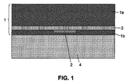
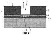
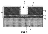
平坦に横たわり、3次元構造を含む基板を得る工程であって、3次元構造は、例えばホールやバイアのような、基板の面に対して実質的に垂直な少なくとも1つの面を含む工程と、
酸性電解質溶液中で基板を陽極酸化することにより3次元構造の上または中に酸化層を形成する工程と、を含む。
Claims (6)
- 半導体基板の上に酸化層を形成する方法であって、
分離領域を有するデバイス基板、多層の相互結合構造、およびデバイス基板と多層の相互結合構造との間の絶縁層を含む半導体基板を得る工程と、
デバイス基板の裏側から絶縁層まで、デバイス基板中に含まれる分離領域を通って少なくとも1つのホールをエッチングする工程と、
酸性の電解質溶液中で基板を陽極酸化することにより、基板の上に酸化層を形成する工程と、を含み、
基板の上に酸化層を形成する工程は、
電解質溶液中に基板を浸責する工程と、
電解質溶液中に配置されたカソードと、デバイス基板からなるアノードとの間に10Vと400Vの間の電位を与え、これにより基板を陽極酸化する工程と、で行われ、
陽極酸化する工程は、
最初に、所定の時間、固定された電流密度が、基板を通って得られるように電位を与える工程と、
所定の時間が経過した後に、10Vと400Vの間の固定された電位を与える工程との、2工程のプロセスで行われる方法。 - 酸性の電解質溶液中で基板を陽極酸化する工程は、クエン酸、酢酸、シュウ酸、硫酸、リン酸、硝酸、またはそれらの組み合わせを含む電解質溶液中に、基板を浸責する工程を含む請求項1に記載の方法。
- 酸性の電解質溶液中で基板を陽極酸化する工程は、0%(含有せず)と20%の間の酸濃度を有する電解質溶液中に基板を浸責する工程を含む請求項1に記載の方法。
- 基板の上に酸化層を形成する工程は、少なくとも1つのホールの側壁に、酸化層を形成する工程を含む請求項1に記載の方法。
- 電位を与える工程は、時間の関数として基板を通る電流密度が変化するように、電位を与えて行われる請求項1に記載の方法。
- 半導体デバイスの製造プロセスにおける、請求項1〜5のいずれかに記載の方法の使用。
Applications Claiming Priority (3)
| Application Number | Priority Date | Filing Date | Title |
|---|---|---|---|
| US5009208P | 2008-05-02 | 2008-05-02 | |
| US61/050,092 | 2008-05-02 | ||
| PCT/EP2009/055312 WO2009133196A1 (en) | 2008-05-02 | 2009-04-30 | Method for providing oxide layers |
Publications (3)
| Publication Number | Publication Date |
|---|---|
| JP2011523202A JP2011523202A (ja) | 2011-08-04 |
| JP2011523202A5 JP2011523202A5 (ja) | 2012-02-09 |
| JP5528430B2 true JP5528430B2 (ja) | 2014-06-25 |
Family
ID=40941299
Family Applications (1)
| Application Number | Title | Priority Date | Filing Date |
|---|---|---|---|
| JP2011506732A Expired - Fee Related JP5528430B2 (ja) | 2008-05-02 | 2009-04-30 | 酸化層の形成方法 |
Country Status (4)
| Country | Link |
|---|---|
| US (1) | US8822330B2 (ja) |
| EP (1) | EP2272087B1 (ja) |
| JP (1) | JP5528430B2 (ja) |
| WO (1) | WO2009133196A1 (ja) |
Families Citing this family (3)
| Publication number | Priority date | Publication date | Assignee | Title |
|---|---|---|---|---|
| US8912522B2 (en) * | 2009-08-26 | 2014-12-16 | University Of Maryland | Nanodevice arrays for electrical energy storage, capture and management and method for their formation |
| US10032569B2 (en) * | 2009-08-26 | 2018-07-24 | University Of Maryland, College Park | Nanodevice arrays for electrical energy storage, capture and management and method for their formation |
| US9219032B2 (en) * | 2012-07-09 | 2015-12-22 | Qualcomm Incorporated | Integrating through substrate vias from wafer backside layers of integrated circuits |
Family Cites Families (16)
| Publication number | Priority date | Publication date | Assignee | Title |
|---|---|---|---|---|
| US4005452A (en) * | 1974-11-15 | 1977-01-25 | International Telephone And Telegraph Corporation | Method for providing electrical isolating material in selected regions of a semiconductive material and the product produced thereby |
| US4849370A (en) * | 1987-12-21 | 1989-07-18 | Texas Instruments Incorporated | Anodizable strain layer for SOI semiconductor structures |
| JP2938152B2 (ja) * | 1990-07-06 | 1999-08-23 | 株式会社東芝 | 半導体装置およびその製造方法 |
| JPH06350064A (ja) * | 1993-06-07 | 1994-12-22 | Canon Inc | 半導体装置及びその実装方法 |
| US5511428A (en) * | 1994-06-10 | 1996-04-30 | Massachusetts Institute Of Technology | Backside contact of sensor microstructures |
| JP3893645B2 (ja) * | 1996-03-18 | 2007-03-14 | ソニー株式会社 | 薄膜半導体装置およびicカードの製造方法 |
| JP2815001B2 (ja) * | 1996-10-21 | 1998-10-27 | 日本電気株式会社 | 薄膜soi基板の製造方法 |
| US5736454A (en) * | 1997-03-20 | 1998-04-07 | National Science Council | Method for making a silicon dioxide layer on a silicon substrate by pure water anodization followed by rapid thermal densification |
| JPH11126906A (ja) * | 1997-10-22 | 1999-05-11 | Semiconductor Energy Lab Co Ltd | 陽極酸化方法 |
| US6352893B1 (en) * | 1999-06-03 | 2002-03-05 | Infineon Technologies Ag | Low temperature self-aligned collar formation |
| DE10147894B4 (de) * | 2001-07-31 | 2007-08-23 | Infineon Technologies Ag | Verfahren zum Füllen von Gräben in integrierten Halbleiterschaltungen |
| DE10138981B4 (de) * | 2001-08-08 | 2005-09-08 | Infineon Technologies Ag | Verfahren zur Bildung von Siliziumoxid durch elektrochemische Oxidation eines Halbleiter-Substrats mit Vertiefungen |
| JP4717290B2 (ja) * | 2001-09-12 | 2011-07-06 | 株式会社フジクラ | 貫通電極の製造方法 |
| US6815315B2 (en) * | 2002-05-14 | 2004-11-09 | Matsushita Electric Works, Ltd. | Method for electrochemical oxidation |
| JP4035066B2 (ja) * | 2003-02-04 | 2008-01-16 | 株式会社ルネサステクノロジ | 半導体装置の製造方法 |
| JP4199206B2 (ja) * | 2005-03-18 | 2008-12-17 | シャープ株式会社 | 半導体装置の製造方法 |
-
2009
- 2009-04-30 JP JP2011506732A patent/JP5528430B2/ja not_active Expired - Fee Related
- 2009-04-30 WO PCT/EP2009/055312 patent/WO2009133196A1/en active Application Filing
- 2009-04-30 EP EP09738240.2A patent/EP2272087B1/en not_active Not-in-force
-
2010
- 2010-10-18 US US12/906,766 patent/US8822330B2/en not_active Expired - Fee Related
Also Published As
| Publication number | Publication date |
|---|---|
| US20110086507A1 (en) | 2011-04-14 |
| US8822330B2 (en) | 2014-09-02 |
| EP2272087B1 (en) | 2018-04-04 |
| EP2272087A1 (en) | 2011-01-12 |
| WO2009133196A1 (en) | 2009-11-05 |
| JP2011523202A (ja) | 2011-08-04 |
Similar Documents
| Publication | Publication Date | Title |
|---|---|---|
| JP6286780B2 (ja) | 無線周波数用途又は電力用途のための電子装置及びそのような装置を製造するためのプロセス | |
| TWI544576B (zh) | 形成全包覆互連線的方法 | |
| CN107408491B (zh) | 氮化铝阻挡层 | |
| JPS5837987B2 (ja) | 埋設酸化物分離領域の形成方法 | |
| TWI374483B (en) | Method for fabricating vertical channel transistor in semiconductor device | |
| US20030008473A1 (en) | Anodizing method and apparatus and semiconductor substrate manufacturing method | |
| EP2458037A1 (en) | A method for precisely controlled masked anodization | |
| JP2004241479A (ja) | 半導体装置の製造方法 | |
| TW200913132A (en) | Method for forming isolation layer in semiconductor device | |
| CN100499064C (zh) | 半导体隔离结构及其形成方法 | |
| JP5528430B2 (ja) | 酸化層の形成方法 | |
| JP2001523050A (ja) | 少なくとも1つのコンデンサを有する回路構造およびその製造方法 | |
| JPH05160342A (ja) | 半導体装置及びその製造方法 | |
| US20160372336A1 (en) | Method for Manufacturing a Semiconductor Device by Hydrogen Treatment | |
| Yan et al. | Facile fabrication of wafer-scale, micro-spacing and high-aspect-ratio silicon microwire arrays | |
| JPH06326077A (ja) | シリコン基板内に孔構造を形成する方法 | |
| CN1512558A (zh) | 形成半导体器件的隔离膜的方法 | |
| JP4625216B2 (ja) | 低温犠牲酸化物形成法 | |
| JP2006261553A (ja) | 半導体装置及びその製造方法 | |
| TWI250552B (en) | Plating apparatus, plating method, and manufacturing method of semiconductor device | |
| TWI237296B (en) | Semiconductor member and the method for manufacturing the same | |
| TW583746B (en) | Method of forming a bottle trench | |
| TWI274381B (en) | Method for fabricating semiconductor device and method for fabricating capacitor in a semiconductor device | |
| KR100808595B1 (ko) | 반도체 소자의 소자분리막 형성 방법 | |
| TW543109B (en) | Formation method of bottle-shaped trench using electrochemical etching |
Legal Events
| Date | Code | Title | Description |
|---|---|---|---|
| A521 | Request for written amendment filed |
Free format text: JAPANESE INTERMEDIATE CODE: A523 Effective date: 20111215 |
|
| A621 | Written request for application examination |
Free format text: JAPANESE INTERMEDIATE CODE: A621 Effective date: 20111215 |
|
| A977 | Report on retrieval |
Free format text: JAPANESE INTERMEDIATE CODE: A971007 Effective date: 20120820 |
|
| A131 | Notification of reasons for refusal |
Free format text: JAPANESE INTERMEDIATE CODE: A131 Effective date: 20120904 |
|
| A521 | Request for written amendment filed |
Free format text: JAPANESE INTERMEDIATE CODE: A523 Effective date: 20121204 |
|
| A131 | Notification of reasons for refusal |
Free format text: JAPANESE INTERMEDIATE CODE: A131 Effective date: 20130402 |
|
| A521 | Request for written amendment filed |
Free format text: JAPANESE INTERMEDIATE CODE: A523 Effective date: 20130702 |
|
| A02 | Decision of refusal |
Free format text: JAPANESE INTERMEDIATE CODE: A02 Effective date: 20131001 |
|
| A521 | Request for written amendment filed |
Free format text: JAPANESE INTERMEDIATE CODE: A523 Effective date: 20140131 |
|
| A911 | Transfer to examiner for re-examination before appeal (zenchi) |
Free format text: JAPANESE INTERMEDIATE CODE: A911 Effective date: 20140207 |
|
| TRDD | Decision of grant or rejection written | ||
| A01 | Written decision to grant a patent or to grant a registration (utility model) |
Free format text: JAPANESE INTERMEDIATE CODE: A01 Effective date: 20140318 |
|
| A61 | First payment of annual fees (during grant procedure) |
Free format text: JAPANESE INTERMEDIATE CODE: A61 Effective date: 20140415 |
|
| R150 | Certificate of patent or registration of utility model |
Ref document number: 5528430 Country of ref document: JP Free format text: JAPANESE INTERMEDIATE CODE: R150 |
|
| R250 | Receipt of annual fees |
Free format text: JAPANESE INTERMEDIATE CODE: R250 |
|
| R250 | Receipt of annual fees |
Free format text: JAPANESE INTERMEDIATE CODE: R250 |
|
| R250 | Receipt of annual fees |
Free format text: JAPANESE INTERMEDIATE CODE: R250 |
|
| R250 | Receipt of annual fees |
Free format text: JAPANESE INTERMEDIATE CODE: R250 |
|
| LAPS | Cancellation because of no payment of annual fees |