JP5528430B2 - Formation method of oxide layer - Google Patents
Formation method of oxide layer Download PDFInfo
- Publication number
- JP5528430B2 JP5528430B2 JP2011506732A JP2011506732A JP5528430B2 JP 5528430 B2 JP5528430 B2 JP 5528430B2 JP 2011506732 A JP2011506732 A JP 2011506732A JP 2011506732 A JP2011506732 A JP 2011506732A JP 5528430 B2 JP5528430 B2 JP 5528430B2
- Authority
- JP
- Japan
- Prior art keywords
- substrate
- oxide layer
- electrolyte solution
- present
- potential
- Prior art date
- Legal status (The legal status is an assumption and is not a legal conclusion. Google has not performed a legal analysis and makes no representation as to the accuracy of the status listed.)
- Expired - Fee Related
Links
Images


Classifications
-
- H—ELECTRICITY
- H01—ELECTRIC ELEMENTS
- H01L—SEMICONDUCTOR DEVICES NOT COVERED BY CLASS H10
- H01L21/00—Processes or apparatus adapted for the manufacture or treatment of semiconductor or solid state devices or of parts thereof
- H01L21/02—Manufacture or treatment of semiconductor devices or of parts thereof
- H01L21/04—Manufacture or treatment of semiconductor devices or of parts thereof the devices having at least one potential-jump barrier or surface barrier, e.g. PN junction, depletion layer or carrier concentration layer
- H01L21/18—Manufacture or treatment of semiconductor devices or of parts thereof the devices having at least one potential-jump barrier or surface barrier, e.g. PN junction, depletion layer or carrier concentration layer the devices having semiconductor bodies comprising elements of Group IV of the Periodic System or AIIIBV compounds with or without impurities, e.g. doping materials
- H01L21/30—Treatment of semiconductor bodies using processes or apparatus not provided for in groups H01L21/20 - H01L21/26
- H01L21/31—Treatment of semiconductor bodies using processes or apparatus not provided for in groups H01L21/20 - H01L21/26 to form insulating layers thereon, e.g. for masking or by using photolithographic techniques; After treatment of these layers; Selection of materials for these layers
- H01L21/314—Inorganic layers
- H01L21/316—Inorganic layers composed of oxides or glassy oxides or oxide based glass
- H01L21/3165—Inorganic layers composed of oxides or glassy oxides or oxide based glass formed by oxidation
- H01L21/31654—Inorganic layers composed of oxides or glassy oxides or oxide based glass formed by oxidation of semiconductor materials, e.g. the body itself
- H01L21/3167—Inorganic layers composed of oxides or glassy oxides or oxide based glass formed by oxidation of semiconductor materials, e.g. the body itself of anodic oxidation
-
- H—ELECTRICITY
- H01—ELECTRIC ELEMENTS
- H01L—SEMICONDUCTOR DEVICES NOT COVERED BY CLASS H10
- H01L21/00—Processes or apparatus adapted for the manufacture or treatment of semiconductor or solid state devices or of parts thereof
- H01L21/02—Manufacture or treatment of semiconductor devices or of parts thereof
- H01L21/02104—Forming layers
- H01L21/02107—Forming insulating materials on a substrate
- H01L21/02225—Forming insulating materials on a substrate characterised by the process for the formation of the insulating layer
- H01L21/02227—Forming insulating materials on a substrate characterised by the process for the formation of the insulating layer formation by a process other than a deposition process
- H01L21/0223—Forming insulating materials on a substrate characterised by the process for the formation of the insulating layer formation by a process other than a deposition process formation by oxidation, e.g. oxidation of the substrate
- H01L21/02233—Forming insulating materials on a substrate characterised by the process for the formation of the insulating layer formation by a process other than a deposition process formation by oxidation, e.g. oxidation of the substrate of the semiconductor substrate or a semiconductor layer
- H01L21/02236—Forming insulating materials on a substrate characterised by the process for the formation of the insulating layer formation by a process other than a deposition process formation by oxidation, e.g. oxidation of the substrate of the semiconductor substrate or a semiconductor layer group IV semiconductor
- H01L21/02238—Forming insulating materials on a substrate characterised by the process for the formation of the insulating layer formation by a process other than a deposition process formation by oxidation, e.g. oxidation of the substrate of the semiconductor substrate or a semiconductor layer group IV semiconductor silicon in uncombined form, i.e. pure silicon
-
- H—ELECTRICITY
- H01—ELECTRIC ELEMENTS
- H01L—SEMICONDUCTOR DEVICES NOT COVERED BY CLASS H10
- H01L21/00—Processes or apparatus adapted for the manufacture or treatment of semiconductor or solid state devices or of parts thereof
- H01L21/02—Manufacture or treatment of semiconductor devices or of parts thereof
- H01L21/02104—Forming layers
- H01L21/02107—Forming insulating materials on a substrate
- H01L21/02225—Forming insulating materials on a substrate characterised by the process for the formation of the insulating layer
- H01L21/02227—Forming insulating materials on a substrate characterised by the process for the formation of the insulating layer formation by a process other than a deposition process
- H01L21/02258—Forming insulating materials on a substrate characterised by the process for the formation of the insulating layer formation by a process other than a deposition process formation by anodic treatment, e.g. anodic oxidation
-
- H—ELECTRICITY
- H01—ELECTRIC ELEMENTS
- H01L—SEMICONDUCTOR DEVICES NOT COVERED BY CLASS H10
- H01L21/00—Processes or apparatus adapted for the manufacture or treatment of semiconductor or solid state devices or of parts thereof
- H01L21/02—Manufacture or treatment of semiconductor devices or of parts thereof
- H01L21/04—Manufacture or treatment of semiconductor devices or of parts thereof the devices having at least one potential-jump barrier or surface barrier, e.g. PN junction, depletion layer or carrier concentration layer
- H01L21/18—Manufacture or treatment of semiconductor devices or of parts thereof the devices having at least one potential-jump barrier or surface barrier, e.g. PN junction, depletion layer or carrier concentration layer the devices having semiconductor bodies comprising elements of Group IV of the Periodic System or AIIIBV compounds with or without impurities, e.g. doping materials
- H01L21/30—Treatment of semiconductor bodies using processes or apparatus not provided for in groups H01L21/20 - H01L21/26
- H01L21/31—Treatment of semiconductor bodies using processes or apparatus not provided for in groups H01L21/20 - H01L21/26 to form insulating layers thereon, e.g. for masking or by using photolithographic techniques; After treatment of these layers; Selection of materials for these layers
- H01L21/314—Inorganic layers
- H01L21/316—Inorganic layers composed of oxides or glassy oxides or oxide based glass
- H01L21/3165—Inorganic layers composed of oxides or glassy oxides or oxide based glass formed by oxidation
- H01L21/31654—Inorganic layers composed of oxides or glassy oxides or oxide based glass formed by oxidation of semiconductor materials, e.g. the body itself
- H01L21/3167—Inorganic layers composed of oxides or glassy oxides or oxide based glass formed by oxidation of semiconductor materials, e.g. the body itself of anodic oxidation
- H01L21/31675—Inorganic layers composed of oxides or glassy oxides or oxide based glass formed by oxidation of semiconductor materials, e.g. the body itself of anodic oxidation of silicon
Description
本発明は、半導体プロセスに関する。更に、本発明は、例えば5以下のアスペクト比(高さに対する幅の比)のような高いアスペクト比を有する3次元構造の基板上の所定の位置に、酸化層を形成する方法に関する。 The present invention relates to a semiconductor process. Furthermore, the present invention relates to a method of forming an oxide layer at a predetermined position on a substrate having a three-dimensional structure having a high aspect ratio, for example, an aspect ratio (a ratio of width to height) of 5 or less.
シリコン酸化物は、半導体プロセス技術で使用される公知の材料である。シリコン酸化物を堆積または成長するために多くの技術が存在する。シリコン酸化物は、シリコンの熱酸化により形成することができる。代わりに、化学気相堆積(CVD)がシリコン酸化物の形成に使用されても良い。このプロセスを用いることにより、典型的には200℃から500℃までの範囲の温度で、プロセスチャンバ中の化学反応により、シリコン酸化物が形成される。この目的のために、例えばシラン(SiH4)、TEOS(テトラエチル・オルソシリケイト−Si(OC2H5)4)、またはHMDSO(ヘキサメチルジシロキサン)のような特定の前駆体が一般に使用される。 Silicon oxide is a known material used in semiconductor process technology. There are many techniques for depositing or growing silicon oxide. Silicon oxide can be formed by thermal oxidation of silicon. Alternatively, chemical vapor deposition (CVD) may be used to form silicon oxide. By using this process, silicon oxide is formed by chemical reactions in the process chamber, typically at temperatures ranging from 200 ° C to 500 ° C. For this purpose, specific precursors such as, for example, silane (SiH 4 ), TEOS (tetraethyl orthosilicate-Si (OC 2 H 5 ) 4 ), or HMDSO (hexamethyldisiloxane) are generally used. .
形成された酸化物の品質(電気的特性および機械的特性)は、主に形成中に酸化物中にトラップされた不純物の量に依存し、このように、その形成に使用された技術にも依存する。不純物は、例えば不完全な前駆体の分解の結果である。 The quality of the oxide formed (electrical and mechanical properties) depends mainly on the amount of impurities trapped in the oxide during formation, and thus also on the technology used for its formation. Dependent. Impurities are for example the result of incomplete precursor decomposition.
高品質の酸化膜を低温で得るために、プラズマ誘起化学気相堆積(PECVD)が使用されて前駆体が効率的に分解される。 In order to obtain high quality oxide films at low temperatures, plasma induced chemical vapor deposition (PECVD) is used to efficiently decompose the precursor.
シリコン酸化物を形成する他の方法は、陽極酸化のようなシリコンの電気化学的酸化による。 Another method of forming silicon oxide is by electrochemical oxidation of silicon, such as anodic oxidation.
米国特許5,736,454には、例えばフィールド酸化層や薄膜トランジスタの酸化層のように、シリコン基板上にシリコン酸化層を形成する方法が開示されている。この方法は、室温で電解反応を行い、アノードとして働くシリコン基板上にシリコン酸化層を形成する工程を含み、電解反応の電解質として純水が使用される。これを得るために、アルミニウム膜がシリコン基板の裏側に蒸着され、陽極酸化のためのアノードコンタクトを形成する。米国特許5,736,454の方法は、例えばゲート酸化膜として使用できる高品質のシリコン酸化層を得るためにはアシスト技術が必要である。それゆえに、形成された二酸化シリコン層は、更に、不活性ガス雰囲気中で、700℃と1000℃との間の温度で、所定の期間、急速熱緻密化が行われ、二酸化シリコンが緻密化される。米国特許5,736,454に記載された方法の欠点は、取り扱いのためにキャリアに取り付ける必要があり、キャリアは非導電性であるような、薄いウエハには適用できないことである。米国特許5,736,454に記載された方法の更なる欠点は、50Åから88Åが20分から100分で形成されるという遅いプロセスである。 US Pat. No. 5,736,454 discloses a method of forming a silicon oxide layer on a silicon substrate, such as a field oxide layer or an oxide layer of a thin film transistor. This method includes a step of performing an electrolytic reaction at room temperature to form a silicon oxide layer on a silicon substrate serving as an anode, and pure water is used as an electrolyte for the electrolytic reaction. To obtain this, an aluminum film is deposited on the back side of the silicon substrate to form an anode contact for anodization. The method of US Pat. No. 5,736,454 requires an assist technique in order to obtain a high-quality silicon oxide layer that can be used as a gate oxide film, for example. Therefore, the formed silicon dioxide layer is further subjected to rapid thermal densification for a predetermined period at a temperature between 700 ° C. and 1000 ° C. in an inert gas atmosphere, and the silicon dioxide is densified. The A disadvantage of the method described in US Pat. No. 5,736,454 is that it must be attached to a carrier for handling, and the carrier is not applicable to thin wafers that are non-conductive. A further disadvantage of the method described in US Pat. No. 5,736,454 is the slow process in which 50 to 88 inches are formed in 20 to 100 minutes.
PECVD堆積は、一般には、200℃と400℃の間の温度で行われる。ICやパッケージの3D集積を覆う、先端のパッケージング応用では、一般的な堆積温度は200℃より低くする必要があり、好適には、例えば、一般には高温には耐えられないポリマー系樹脂で接着されるキャリアウエハ上での処理ができるように、100℃より低くする必要がある。PECVDを用いた場合、200℃より低い温度、時には80℃まで低くして層を堆積することが可能であるが、そのような温度で堆積した酸化物は、例えば低い機械的特性のような劣った特性を示す。層は、低い破壊電界とピンホールの欠点を持つ。また、堆積層の適合性が低く、即ち、深い3D構造では堆積層の膜厚は均一では無い。 PECVD deposition is generally performed at a temperature between 200 ° C and 400 ° C. For advanced packaging applications covering 3D integration of ICs and packages, the typical deposition temperature should be lower than 200 ° C., preferably bonded with, for example, a polymer resin that generally cannot withstand high temperatures It is necessary to make the temperature lower than 100 ° C. so that the processing on the carrier wafer can be performed. When using PECVD, it is possible to deposit layers at temperatures below 200 ° C., sometimes as low as 80 ° C., but oxides deposited at such temperatures are inferior, for example, poor mechanical properties. Show the characteristics. The layer has the disadvantages of low breakdown field and pinholes. Also, the suitability of the deposited layer is low, that is, the thickness of the deposited layer is not uniform in a deep 3D structure.
シリコンの酸化は、良好な品質の酸化物を得るには、前処理、追加のアシスト技術、または特別な基板準備が必要な困難なプロセスである。例えば良好な品質の酸化物は、100nA/cm2より低い寄生リーク電流を有する。 Silicon oxidation is a difficult process that requires pre-treatment, additional assist techniques, or special substrate preparation to obtain good quality oxides. For example, a good quality oxide has a parasitic leakage current lower than 100 nA / cm 2 .
更に、バイア構造が基板上に形成された場合、リソグラフィパターニングに使用するスキャナの小さな焦点深さおよび/または反射効果によるリソグラフィ限界のために、それらのバイア構造の内側に酸化物を形成することは困難である。 In addition, when via structures are formed on a substrate, it is not possible to form oxides inside those via structures due to lithography limitations due to the small depth of focus and / or reflection effects of scanners used for lithographic patterning. Have difficulty.
本発明の具体例の目的は、例えばシリコン基板のような半導体基板の上または中の、3次元(3D)構造上のような、半導体基板上に、酸化層を形成する方法を提供することである。 An object of embodiments of the present invention is to provide a method of forming an oxide layer on a semiconductor substrate, such as on a three-dimensional (3D) structure, for example on or in a semiconductor substrate such as a silicon substrate. is there.
本発明の特定の具体例にかかる方法では、酸化層は、例えば半導体基板中のトレンチまたはホールの側壁に、および/または半導体基板の主表面の柱の側壁のような、半導体基板の中または上の3D構造上に形成されても良い。 In the method according to certain embodiments of the invention, the oxide layer is present in or on the semiconductor substrate, such as, for example, on the sidewalls of trenches or holes in the semiconductor substrate and / or on the pillar sidewalls of the main surface of the semiconductor substrate. It may be formed on the 3D structure.
本発明の具体例にかかる方法は、例えば室温のような、80℃より低いような低温で適用される。 The method according to embodiments of the present invention is applied at low temperatures, such as room temperature, such as below 80 ° C.
上記目的は、本発明にかかる方法およびデバイスにより達成される。 The above objective is accomplished by a method and device according to the present invention.
第1の形態では、本発明は、例えば半導体基板の中または上の3次元構造上のような半導体基板上に酸化層を形成する方法を提供する。この方法は、
半導体基板を得る工程と、
酸性電解質溶液中で基板を陽極酸化することにより、基板上に酸化層を形成する工程と、を含む。
In a first aspect, the present invention provides a method for forming an oxide layer on a semiconductor substrate, such as on a three-dimensional structure in or on the semiconductor substrate. This method
Obtaining a semiconductor substrate;
Forming an oxide layer on the substrate by anodizing the substrate in an acidic electrolyte solution.
基板が三次元構造を含むような特別な具体例では、そのような3次元構造は、例として、基板貫通バイア(TSV:through-substrate via)のための円柱またはドーナツ形状のホールでも良い。代わりの具体例では、例えばMEMSデバイスを形成するための、基板の表面上に形成されたあらゆる形状でも良い。3次元構造は、トレンチ、ホール、および/または柱を含む。 In particular embodiments where the substrate includes a three-dimensional structure, such a three-dimensional structure may be, for example, a cylindrical or donut shaped hole for a through-substrate via (TSV). In alternate embodiments, any shape formed on the surface of the substrate, eg, to form a MEMS device, may be used. The three-dimensional structure includes trenches, holes, and / or pillars.
酸性の電解質溶液中で基板を陽極酸化する工程は、クエン酸、酢酸、シュウ酸、硫酸、リン酸、硝酸、またはそれらの組み合わせのいずれかを含む電解質溶液中に基板を浸責する工程を含む。本発明の具体例では、電解質溶液中の酸の濃度は、使用される酸と特定の環境に依存して、0%(含有しない)と20%の間でもよい。 Anodizing the substrate in the acidic electrolyte solution includes immersing the substrate in an electrolyte solution comprising any of citric acid, acetic acid, oxalic acid, sulfuric acid, phosphoric acid, nitric acid, or combinations thereof. . In embodiments of the invention, the concentration of acid in the electrolyte solution may be between 0% (not contained) and 20%, depending on the acid used and the particular environment.
酸性電解質溶液では、非酸性の電解質溶液を用いた場合に比較して、陽極酸化の速度が増加することが、本発明の具体例の長所である。このように、より厚い酸化層が、より短時間で形成できる。陽極酸化プロセスの速度は、電解質溶液中の酸の濃度に依存する。 In the acidic electrolyte solution, it is an advantage of the specific example of the present invention that the anodic oxidation rate is increased as compared with the case where the non-acidic electrolyte solution is used. Thus, a thicker oxide layer can be formed in a shorter time. The rate of the anodization process depends on the acid concentration in the electrolyte solution.
本発明の具体例にかかる方法を用いた場合、酸化層は、例えば電解質中に基板が露出した位置のような、所定の位置に形成することができる。そのような所定の位置は、例えば、3次元構造の主表面上、および/またはトレンチやホールやバイアの側壁のようなその側壁のような、3次元構造の部分を含む。 When the method according to the embodiment of the present invention is used, the oxide layer can be formed at a predetermined position such as a position where the substrate is exposed in the electrolyte. Such predetermined locations include, for example, portions of the three-dimensional structure on the major surface of the three-dimensional structure and / or its sidewalls such as the sidewalls of trenches, holes and vias.
陽極酸化を使用する長所は、陽極酸化電解質に露出した基板表面上の均一な酸化物膜厚と、同時に表面粗れの低減を実現することである。基板中での垂直トレンチやバイアのエッチングは、一般には粗れた側壁(スカラプス:scallops)となる。基板表面上の鋭い表面形状(例えば、スカラプス)は、局所的に高い静電場となり、それらの位置で陽極酸化プロセスを加速させ、これにより自然な方法で表面を平坦化する。酸化物の平坦な表面、またはこのようにして低減された粗さは、例えば絶縁破壊に対する耐性を改良するような、良好な電気的特性を与える。 The advantage of using anodization is that it achieves a uniform oxide film thickness on the substrate surface exposed to the anodizing electrolyte and simultaneously reduces surface roughness. Etching vertical trenches and vias in the substrate generally results in rough sidewalls (scallops). Sharp surface features (eg, scallops) on the substrate surface result in locally high electrostatic fields that accelerate the anodization process at those locations, thereby planarizing the surface in a natural way. The flat surface of the oxide, or the roughness thus reduced, provides good electrical properties, for example improving the resistance to breakdown.
本発明の具体例にかかる方法の他の特徴は、例えば80℃より低い温度、更には50℃より低い温度、例えば室温のような低温で行えることである。 Another feature of the method according to embodiments of the present invention is that it can be carried out at a temperature lower than, for example, 80 ° C., or even lower than 50 ° C., such as room temperature.
本発明の具体例にかかる方法では、例えば基板貫通バイアのようなバイア、またはMEMSデバイスを形成するために使用できる。 The method according to embodiments of the present invention can be used to form vias, such as through-substrate vias, or MEMS devices.
本発明の具体例で基板上に酸化層を形成する工程は、
基板を電解質溶液中に浸責する工程と、
電解質溶液中のカソードと、基板上または基板により形成されたアノードとの間に電位を与え、これにより基板を陽極酸化する工程と、で行われる。基板が3次元構造を含む場合、この構造は基板と一緒に陽極酸化される。電位を与えることにより、電池を通って電流が流れる。陽極層が成長すると、プロセスを行い続けるために、(一定の電流では)より大きな電位が必要となる。所定の電圧に達した場合、所定の酸化物膜厚が達成される。電圧が一定に維持された場合、残りの陽極酸化時間の間に電流が指数関数的に減少し、その間に陽極酸化層中の欠陥が治癒されて酸化物が緻密化される。
In the specific example of the present invention, the step of forming the oxide layer on the substrate includes:
Immersing the substrate in the electrolyte solution;
Applying a potential between the cathode in the electrolyte solution and the anode formed on or by the substrate, thereby anodizing the substrate. If the substrate includes a three-dimensional structure, this structure is anodized together with the substrate. By applying a potential, current flows through the battery. As the anode layer grows, a higher potential (at a constant current) is required to continue the process. When a predetermined voltage is reached, a predetermined oxide film thickness is achieved. If the voltage is kept constant, the current decreases exponentially during the remaining anodization time, during which the defects in the anodized layer are healed and the oxide is densified.
本発明の具体例では、形成された酸化層は、基板の表面側に形成される。カソードとアノードとの間に電位を与える工程は、カソードと、基板の表面上に位置するアノードとの間に電位を与える工程を含む。これは、非常に薄い基板を用いる方法で有利である。そのような薄い基板は、取り扱いに便利なように、取り扱いウエハ上に配置する。そのような取り扱いウエハは、大部分の場合、非導電性である。カソードと、基板の表面側のアノードとの間に電位を与えるために、取り扱いの有無や型は陽極酸化プロセスには関係しない。 In the embodiment of the present invention, the formed oxide layer is formed on the surface side of the substrate. The step of applying a potential between the cathode and the anode includes the step of applying a potential between the cathode and the anode located on the surface of the substrate. This is advantageous in a method using a very thin substrate. Such a thin substrate is placed on a handling wafer for convenient handling. Such handling wafers are mostly non-conductive. Since the potential is applied between the cathode and the anode on the surface side of the substrate, the presence / absence and type of handling are not related to the anodizing process.
与えられた電位は、10Vと400Vの間でも良い。電流は、電解質溶液の電気分解を開始するために十分高くなければならない。 The applied potential may be between 10V and 400V. The current must be high enough to initiate electrolysis of the electrolyte solution.
本発明の具体例では、電解質溶液中に配置されやカソードと、基板の上またはそばに形成されたアノードとの間に電位を与える工程は、時間の関数として基板を通る電流密度を変えるように電位を与える工程でも良い。このように、与えられた電位は、時間の関数として変化しても良い。 In an embodiment of the present invention, the step of applying a potential between the cathode placed in the electrolyte solution and the anode formed on or near the substrate will change the current density through the substrate as a function of time. A step of applying a potential may be used. Thus, the applied potential may change as a function of time.
本発明の具体例では、陽極酸化は2工程のプロセスで行われても良い。それらの具体例では、電解質溶液中に配置されやカソードと、基板の上またはそばに形成されたアノードとの間に電位を与える工程は、
最初に、所定の時間、酸化層を形成するために、固定された電流密度が、基板を通って得られ、
所定の時間が経過した後に、固定された電位が、酸化層を治癒するために得られる。
In embodiments of the present invention, anodic oxidation may be performed in a two-step process. In those embodiments, the step of applying a potential between the cathode disposed in the electrolyte solution and the anode formed on or near the substrate comprises:
First, a fixed current density is obtained through the substrate to form an oxide layer for a predetermined time,
After a predetermined time has elapsed, a fixed potential is obtained to heal the oxide layer.
酸化層の治癒は、ピンホールのような欠陥を除去し、良好な品質の酸化層を得ることを意味する。 The healing of the oxide layer means removing defects such as pinholes and obtaining a good quality oxide layer.
更なる形態では、本発明は、半導体デバイスの製造プロセス中での、本発明の具体例にかかる方法の使用である。 In a further aspect, the present invention is the use of a method according to embodiments of the present invention during a semiconductor device manufacturing process.
他の形態では、本発明は、本発明の具体例にかかる方法により形成された酸化層を有する基板を提供することである。 In another aspect, the present invention provides a substrate having an oxide layer formed by a method according to embodiments of the present invention.
更なる形態では、本発明は、基板上に、少なくともホールを含む3次元構造を形成するものである。3次元構造は、更に、3次元構造の主表面上の、および/または少なくとも1つのホールの側壁の、酸化層を含み、この酸化層は、本発明の具体例にかかる方法により形成される。例えばトレンチのような高いアスペクト比の3次元構造中で形成された酸化層が等角になることが特に有用である。公知の低温プロセスは、一般には10%より少ないステップカバレジを有し、ところが本発明の具体例で形成した酸化層はCVD酸化物のように等角であり、低温で形成される。 In a further aspect, the present invention forms a three-dimensional structure including at least holes on a substrate. The three-dimensional structure further includes an oxide layer on the major surface of the three-dimensional structure and / or on the sidewalls of at least one hole, the oxide layer being formed by a method according to embodiments of the present invention. It is particularly useful that the oxide layer formed in a three-dimensional structure with a high aspect ratio, such as a trench, is equiangular. Known low temperature processes generally have a step coverage of less than 10%, whereas the oxide layer formed in embodiments of the present invention is conformal like CVD oxide and is formed at low temperatures.
本発明の特別で好ましい形態は、添付した独立請求項および従属請求項に表される。従属請求項の特徴は、必要に応じて、独立請求項の特徴や他の従属請求項の特徴と組み合わせても良く、単に請求項に表された通りだけではない。 Particular and preferred aspects of the invention are set out in the accompanying independent and dependent claims. The features of the dependent claims may be combined with the features of the independent claims and with the features of other dependent claims as appropriate and not merely as expressed in the claims.
本発明の、上記および他の特徴、性質、および優位性は、本発明の原理を例示により示す添付の図面と共に、以下の詳細な記載から明らかになるであろう。この説明は例示のみを目的とし、本発明の範囲を限定するものではない。以下で用いられる参照符号は、添付の図面を引用する。 The above and other features, characteristics and advantages of the present invention will become apparent from the following detailed description, taken in conjunction with the accompanying drawings, illustrating by way of example the principles of the invention. This description is for illustrative purposes only and is not intended to limit the scope of the present invention. The reference numerals used in the following refer to the attached drawings.
異なる図面において、同一参照番号は、同一または類似の要素を示す。 In the different figures, the same reference signs refer to the same or analogous elements.
本発明は、特定の具体例に関して、所定の図面を参照しながら説明されるが、本発明はそれらに限定されるものではなく、請求の範囲によってのみ限定されるものである。記載された図面は、単に概略であり限定するものではない。図面において、幾つかの要素の大きさは、図示を目的として拡大され、縮尺通りには記載されない。寸法と、対応する寸法は、本発明の現実の実施化に対応しない。 The present invention will be described with respect to particular embodiments and with reference to certain drawings but the invention is not limited thereto but only by the claims. The drawings described are only schematic and are non-limiting. In the drawings, the size of some of the elements are enlarged for illustrative purposes and are not drawn to scale. The dimensions and corresponding dimensions do not correspond to the actual implementation of the present invention.
更に、説明や請求の範囲中の、第1、第2等の用語は、類似の要素の間で区別するために使用され、時間的、空間的に、ランクや他の方法で順序を表す必要はない。そのように使用される用語は、適当な状況下で入替え可能であり、ここに記載された発明の具体例は、ここの説明や図示されたものと異なる順序によっても操作できることを理解すべきである。 In addition, the terms first, second, etc. in the description and in the claims are used to distinguish between similar elements, and must be ordered in time and space, rank and other ways. There is no. It is to be understood that the terms so used are interchangeable under appropriate circumstances and that the embodiments of the invention described herein may be operated in a different order than that described or illustrated herein. is there.
また、説明や請求の範囲中の、上、下等の用語は、記載目的のために使用され、相対的な位置を示すものではない。そのように使用される用語は、適当な状況下で入替え可能であり、ここに記載された発明の具体例は、ここに説明や図示されたものと異なる位置でも操作できることを理解すべきである。 Further, terms such as “upper” and “lower” in the description and the claims are used for description purposes and do not indicate relative positions. It is to be understood that the terms so used are interchangeable under appropriate circumstances and that the embodiments of the invention described herein can be operated at different locations than those described or illustrated herein. .
また、請求の範囲で使用される「含む(comprising)」の用語は、それ以降に示される要素に限定して解釈されること排除するものであり、他の要素や工程を排除しない。このように、言及された特徴、数字、工程、または成分は、その通りに存在するものと解釈され、1またはそれ以上の他の特徴、数字、工程、または成分、またはこれらの組み合わせの存在または追加を排除してはならない。このように、「手段AおよびBを含むデバイス」の表現の範囲は、構成要素AとBのみを含むデバイスに限定されるべきではない。本発明では、単にデバイスに関連した構成要素がAとBであることを意味する。 Further, the term “comprising” used in the claims excludes being interpreted as being limited to the elements shown thereafter, and does not exclude other elements and steps. Thus, any feature, number, step or ingredient referred to is intended to be present as such and the presence or absence of one or more other features, numbers, steps or components, or combinations thereof. Do not exclude additions. Thus, the scope of the expression “a device including means A and B” should not be limited to devices including only components A and B. In the present invention, it simply means that the components related to the device are A and B.
この明細書を通じて参照される「一の具体例(one embodiment)」または「ある具体例(an embodiment)」は、この具体例に関係して記載された特定の長所、構造、または特徴は、本発明の少なくとも1つの具体例に含まれることを意味する。このように、この明細書を通して多くの場所の「一の具体例(one embodiment)」または「ある具体例(an embodiment)」の語句の表現は、同じ具体例を表す必要はなく、表しても構わない。更に、特定の長所、構造、または特徴は、この記載から当業者に明らかなように、1またはそれ以上の具体例中で適当な方法で組み合わせることができる。 “One embodiment” or “an embodiment” referred to throughout this specification is intended to describe certain advantages, structures, or features described in connection with this embodiment. It is meant to be included in at least one embodiment of the invention. Thus, throughout this specification, the phrase “one embodiment” or “an embodiment” in many places need not represent the same embodiment, I do not care. Furthermore, certain advantages, structures, or features may be combined in any suitable manner in one or more embodiments, as will be apparent to those skilled in the art from this description.
同様に、本発明の例示の記載中において、能率的に開示し、多くの発明の形態の1またはそれ以上の理解を助ける目的で、本発明の多くの長所は、時には1つの具体例、図面、またはその記載中にまとめられることを評価すべきである。しかしながら、この開示の方法は、請求される発明がそれぞれの請求項に記載されたものより多くの特徴を必要とすることを意図して表されていると解釈すべきではない。むしろ、以下の請求項が表すように、発明の態様は、1つの記載された具体例の全ての長所より少なくなる。このように詳細な説明に続く請求の範囲は、これにより詳細な説明中に明確に含まれ、それぞれの請求項は、この発明の別々の具体例としてそれ自身で成立する。 Similarly, in the description of exemplary embodiments of the present invention, for the purpose of efficiently disclosing and assisting in understanding one or more of the many inventive forms, many of the advantages of the present invention may sometimes be found in one embodiment, drawing. Or should be summarized in the description. This method of disclosure, however, is not to be interpreted as intending that the claimed invention requires more features than are recited in each claim. Rather, as the following claims indicate, aspects of the invention are less than all the advantages of one described embodiment. Thus, the claims following the detailed description are hereby expressly included in the detailed description, with each claim standing on its own as a separate embodiment of this invention.
更に、ここで記載された幾つかの具体例は、他の具体例に含まれる以外の幾つかの特徴を含み、異なった具体例の長所の組み合わせは、本発明の範囲に入ることを意味し、当業者に理解されるように異なった具体例を形成する。例えば、以下の請求の範囲では、請求された具体例のいくつかは、他の組み合わせにおいても使用することができる。 Further, some embodiments described herein include some features other than those included in other embodiments, and combinations of advantages of different embodiments are meant to be within the scope of the present invention. Different embodiments are formed as will be understood by those skilled in the art. For example, in the following claims, some of the claimed embodiments can be used in other combinations.
ここで与えられる記載において、多くの特別な細部が示される。しかしながら、本発明の具体例はそれらの特別な細部無しに実施できることを理解すべきである。他の例では、公知の方法、構造、および技術は、この記載の理解をわかりにくくしないために、詳細には示されていない。 In the description provided herein, many specific details are set forth. However, it should be understood that embodiments of the invention may be practiced without these specific details. In other instances, well-known methods, structures and techniques have not been shown in detail in order not to obscure the understanding of this description.
本発明は、例えばシリコンプロセスのような半導体プロセスの分野に関し、例えば貫通基板バイアプロセスや半導体ベースのMEMS技術に関する。本発明の特別な具体例では、半導体はシリコンでも良い。 The present invention relates to the field of semiconductor processes, such as silicon processes, for example, to through-substrate via processes and semiconductor-based MEMS technology. In a particular embodiment of the invention, the semiconductor may be silicon.
本発明は、例えばホールのような3次元構造を有する基板に関連して詳細に述べられる。しかしながら、これは本発明を限定することを意図するものではない。本発明は、また、柱である3次元構造や柱状の形状を有する3次元構造を有する基板に、他の型の3次元構造を備えた基板に、または平坦な基板に適用することができる。 The invention will be described in detail in connection with a substrate having a three-dimensional structure, for example a hole. However, this is not intended to limit the invention. The present invention can also be applied to a substrate having a three-dimensional structure that is a pillar or a three-dimensional structure having a columnar shape, a substrate having another type of three-dimensional structure, or a flat substrate.
3次元半導体構造上に、特にホールや突出部の垂直な側壁上に等角な酸化層を形成することは、特に大きなアスペクト比(3次元構造の幅寸法を高さ寸法で割った比として定義され、幅寸法は平坦な基板表面で実質的に測定され、高さ寸法は実質的にその垂線として測定される)、例えば5より小さいアスペクト比や、低温プロセス、例えば80℃より低い温度でのプロセスでは非常に困難である。本発明は、例えばシリコン基板のような3次元半導体の露出した半導体表面領域上に酸化層を形成する方法を提供する。この方法は、
平坦に横たわり、3次元構造を含む基板を得る工程であって、3次元構造は、例えばホールやバイアのような、基板の面に対して実質的に垂直な少なくとも1つの面を含む工程と、
酸性電解質溶液中で基板を陽極酸化することにより3次元構造の上または中に酸化層を形成する工程と、を含む。
The formation of a conformal oxide layer on the three-dimensional semiconductor structure, especially on the vertical sidewalls of the holes and protrusions, is defined as a particularly large aspect ratio (ratio of the width dimension of the three-dimensional structure divided by the height dimension). The width dimension is substantially measured on a flat substrate surface and the height dimension is substantially measured as its normal)), eg at an aspect ratio of less than 5 or at low temperature processes, eg at temperatures below 80 ° C. It is very difficult in the process. The present invention provides a method of forming an oxide layer on an exposed semiconductor surface region of a three-dimensional semiconductor such as a silicon substrate. This method
Lying flat and obtaining a substrate comprising a three-dimensional structure, the three-dimensional structure comprising at least one surface substantially perpendicular to the surface of the substrate, such as holes or vias;
Forming an oxide layer on or in the three-dimensional structure by anodizing the substrate in an acidic electrolyte solution.
陽極酸化は、表面を電解質溶液中に配置しながら、不活性な材料から形成されたカソード(負電極)とアノード(正電極)との間に電位を与えることにより表面が陽極酸化される電気化学プロセスである。アノードは、処理される部分でも良く、または処理される部分の上に更に提供されても良い。与えられた電位の結果、電解質溶液を通って直流電流が流れるため、酸化層が続いて成長される。この電流は、カソードにおいて水素を、アノードの表面において酸素を発生させ、これにより酸化層の積層が形成される。 Anodization is an electrochemistry in which a surface is anodized by applying a potential between a cathode (negative electrode) and an anode (positive electrode) formed from an inert material while the surface is placed in an electrolyte solution. Is a process. The anode may be the part to be treated or may be further provided on the part to be treated. As a result of the applied potential, a direct current flows through the electrolyte solution so that an oxide layer is subsequently grown. This current generates hydrogen at the cathode and oxygen at the surface of the anode, thereby forming a stack of oxide layers.
陽極酸化では、室温で酸化物が成長できる。陽極酸化を用いることにより、3次元(3D)構造のホールの中や突出部の上に酸化層が形成できる。このように、3D構造のホールの中や突出部の上に酸化層を形成するために陽極酸化を用いることにより、本発明の具体例にかかる方法は、化学気相堆積(CVD)技術のような従来のプロセスの限界を克服し、プロセスを単純化でき、結果としてコストを低減できる。 In anodic oxidation, an oxide can grow at room temperature. By using anodization, an oxide layer can be formed in a hole having a three-dimensional (3D) structure or on a protruding portion. Thus, by using anodic oxidation to form an oxide layer in a 3D structure hole or over a protrusion, the method according to embodiments of the present invention is similar to a chemical vapor deposition (CVD) technique. Can overcome the limitations of conventional processes and simplify the process, resulting in lower costs.
本発明の具体例では、陽極酸化プロセスは、酸性の電解質溶液中で行われる。電解質溶液は、例えばクエン酸、酢酸、シュウ酸、硫酸、リン酸、硝酸、またはそれらの組み合わせのいずれかを含んでも良い。電解質溶液中の酸性成分が、陽極酸化プロセスをスピードアップさせることが見出された。それゆえに、酸性の電解質溶液を用いることにより、同じパラメータ(出発材料、電流、温度等)で、他の酸性でない電解質溶液を用いた陽極酸化プロセスに比較して、一定の時間で、より厚い酸化物が成長できる。より酸性の電解質溶液では、より速く陽極酸化プロセスが起きる。 In an embodiment of the invention, the anodization process is performed in an acidic electrolyte solution. The electrolyte solution may include, for example, any of citric acid, acetic acid, oxalic acid, sulfuric acid, phosphoric acid, nitric acid, or combinations thereof. It has been found that acidic components in the electrolyte solution speed up the anodization process. Therefore, by using an acidic electrolyte solution, the same parameters (starting material, current, temperature, etc.), a thicker oxidation in a certain time compared to an anodic oxidation process using other non-acidic electrolyte solutions. Things can grow. With a more acidic electrolyte solution, the anodization process occurs faster.
陽極酸化は、陽極酸化電解質に露出した、Siのような半導体表面上で、均一な酸化物膜厚を実現できる。酸化層の膜厚は、陽極酸化電流を決定する、カソードとアノードとの間の陽極酸化電圧で決定される。 Anodization can achieve a uniform oxide film thickness on a semiconductor surface, such as Si, exposed to the anodizing electrolyte. The thickness of the oxide layer is determined by the anodic oxidation voltage between the cathode and the anode, which determines the anodic oxidation current.
陽極酸化は、また、同時に表面粗さの低減を行う。例えばSiのような半導体材料中に、垂直なトレンチやバイアをエッチングすると、一般に、粗い側壁(スカラプス)となる。例えばSi表面のような半導体表面上の鋭い表面形状(例えばスカラプス)は、より高い静電場となり、それらの位置において陽極酸化プロセスを加速させ、それにより自然な方法で表面を平坦化する。 Anodization also reduces surface roughness at the same time. For example, etching vertical trenches and vias in a semiconductor material such as Si generally results in rough sidewalls. Sharp surface features (eg, scallops) on a semiconductor surface, such as a Si surface, result in higher electrostatic fields, accelerating the anodization process at those locations, thereby planarizing the surface in a natural way.
本発明の具体例は、半導体基板の上または中に形成された3次元構造(3D)構造の上または中に酸化層を形成するための陽極酸化プロセスの使用を提供する。 Embodiments of the present invention provide for the use of an anodization process to form an oxide layer on or in a three-dimensional structure (3D) structure formed on or in a semiconductor substrate.
これ以降、本発明の具体例にかかる方法は、例示の方法で、図1〜図4を参照しながら説明する。これは説明を容易にするためであり、この例は如何なる方法においても本発明を限定することを意図しないことを理解すべきである。本発明の具体例にかかる方法は、基板および/または3D構造が、金属や半導体材料のような導電性材料を含む限り、基板上に3D構造の酸化層を形成するのに使用できる。 Hereinafter, the method according to the embodiment of the present invention will be described by way of example with reference to FIGS. This is for ease of explanation and it should be understood that this example is not intended to limit the invention in any way. The method according to embodiments of the present invention can be used to form an oxide layer of 3D structure on a substrate as long as the substrate and / or 3D structure includes a conductive material such as a metal or semiconductor material.
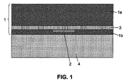
第1の工程では、例えばSi基板のようなデバイス基板1aが提供される。デバイス構造1aの上に、酸化物や窒化物のような誘電体絶縁層3が形成される。誘電体絶縁層3は、単層または複数の層からなっても良い。デバイス基板1aと誘電体絶縁層3との間の界面近傍で、トランジスタ(図示せず)のような能動デバイスが、例えばフロントエンドオブラインのようにデバイス基板1aに形成されても良い。代わりの具体例では、デバイス基板1aは、受動基板である。誘電体絶縁層3の他の側には、例えばデバイスウエハのバックエンドオブラインや半導体挿入(MCM)基板のビルドアップ層のような、絶縁体層と相互結合層とを含む多層の相互結合構造1bが形成される。そのような多層の相互結合構造の1つのコンタクト2が、図1に、模式的に表されて、参照番号2で示される。デバイス基板1aが薄い場合、上述のように複数の層やデバイスで形成された基板は、選択的にキャリア基板4に取り付けられても良い。
In the first step, a
基板1は、300μmより小さい膜厚を有してもよく、例えば50μmと300μmの間の膜厚を有しても良い。本発明の具体例では、例えば半導体基板、特にシリコン基板のように、電流を流すことができ、酸化できる限り、如何なる基板でも使用できる。例えば、陽極酸化される部分である基板1、特にそのデバイス基板1aは、低抵抗のシリコンを含んでも良い。低抵抗シリコンは、30μOhm・cm、またはそれより低い抵抗率を有するが、本発明はこれに限定されるものではない。この目的のために、例えばn−またはp−ドープされたシリコンのような、n−またはp−ドープされた半導体材料が用いられても良い。
The
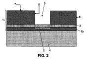
図2に示すように、適切な半導体技術を用いて、ホール5が、半導体デバイスウエハ1aの裏側から、絶縁層3までエッチングされる。一般的な技術は、斜めまたはまっすぐな側壁8を得るための、ICP−RIEプラズマエッチング技術の使用である。それらのホール5は、円、多角形、リング形状、または幾つかの名前であるトレンチのような、様々な形状を有する。
As shown in FIG. 2, the
次に、陽極酸化が行われる。これにより、基板1は酸性の電解質溶液に浸責され、電解質溶液中に配置されたカソードと、基板1の上または基板のそばに形成されたアノードとの間に電位が与えられる。与えられた電位は、10Vと400Vの間でも良い。本発明の具体例では、基板1の材料、特にデバイス基板1aの材料は、それ自体がアノードとして働いても良い。本発明の他の具体例では、アノードが基板1の上に形成されて、基板1の導電性材料に電気的コンタクトを形成しても良い。後者の場合、10kΩと100kΩの間のコンタクトオーミック抵抗が、電極と基板1との間に存在しても良い。このコンタクトは、酸性溶液からコンタクトを保護できる、プラスチックモールド中埋め込まれた電極のセットを配置することで実現できる。そのような電極の例を図12に示す。図12に示される電極60は、電極60と取り囲む電解質溶液80との間の直接的な接触を防止するコンタクトシールリング50により覆われて、電極は、酸性の電解質溶液によって汚染されたり破壊されたりしない。コンタクトシールリング50は、電解質溶液の酸性の影響から、電極60を保護するのに適した材料からなる。電極60は、例えば薄い半導体ウエハのような基板40と、その表面側で電気的にコンタクトし、即ち、本発明の具体例にかかる陽極酸化により酸化層70が形成されるのと同じ側にコンタクトする。取り扱いの容易さのために、酸化される基板40は、例えば一時的な接着剤30の手段により、キャリアウエハ20の上に取り付けられても良い。陽極酸化プロセスの間に、選択的にキャリアウエハ20の上に配置され、一時的に取り付けられた基板40は、ホルダーチャック10の上に配置される。
Next, anodization is performed. As a result, the
デバイス基板1a自身を、配置された電極として使用することは、特に有利である。このように、基板1の裏面にアノードを形成する必要が無く、記載された例では、キャリア基板4の裏に取り付けられる。
It is particularly advantageous to use the
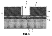
電解質溶液は、例えば、クエン酸、酢酸、シュウ酸、硫酸、リン酸、硝酸、またはそれらの組み合わせのいずれかを含む。基板1に電圧を与えることにより、電解質溶液を通って電流が流れ、これにより電解質溶液と接触した導電性材料の陽極酸化を引き起こす。結果として、シリコン酸化層9が、例えば主表面7のような全ての露出したシリコン表面上に形成されるとともに、3D構造の側壁8上にも形成される(図3)。
The electrolyte solution includes, for example, any of citric acid, acetic acid, oxalic acid, sulfuric acid, phosphoric acid, nitric acid, or combinations thereof. By applying a voltage to the
陽極酸化プロセスが、絶縁体3に対して選択的であることがわかる。これは、露出した導電性基板材料にのみ酸化物が形成され、実質的に隣接する非導電体または非導電性材料の上には形成されないことを意味する。
It can be seen that the anodization process is selective to the
主表面7および側壁8の上への例えばシリコン酸化層のような酸化層9の形成は単に一例であり、本発明の他の具体例では、この方法は、少なくとも1つのホール5の側壁8の上のみに、例えばシリコン酸化層のような酸化層を形成するために使用しても良いことが理解される。これは、例えば最初に3D構造の主表面7に絶縁層を形成し、続いて被覆されていない部分、即ち、少なくとも1つのホール5の側壁8を陽極酸化して、例えばシリコン酸化層のような酸化層9を少なくとも1つのホール5の側壁8の上に形成することで行っても良い。
The formation of an oxide layer 9 such as a silicon oxide layer on the
陽極酸化は自己制御性のプロセスであり、これは、陽極酸化のために与えられる電位と、形成される酸化層9の膜厚との間に平衡が存在することを意味する。本発明の具体例では、200nmまでの膜厚の酸化層9の形成が可能である。具体例により、例えばシリコン酸化層のような酸化層9に要求される膜厚に依存して、約10分と10時間との間の時間で陽極酸化が行われる。 Anodization is a self-controlling process, which means that an equilibrium exists between the potential applied for anodization and the thickness of the oxide layer 9 formed. In the specific example of the present invention, the oxide layer 9 having a thickness of up to 200 nm can be formed. According to a specific example, anodization is performed in a time between about 10 minutes and 10 hours, depending on the film thickness required for the oxide layer 9 such as a silicon oxide layer.
本発明の具体例では、陽極酸化プロセスは2工程のプロセスでも良い。第1段階では、カソードとアノードとの間に電位が与えられ、酸化層9を形成することができる固定された電流密度が得られる。第2段階では、与えられる電位は、形成された例えばシリコン酸化層のような酸化層9の治癒が可能な、固定された電位である。酸化シリコンのような酸化層9を治癒は、ピンホールのような欠陥を除去して、良好な品質の酸化層を得ることを意味する。特定の具体例では、化学量論的な酸化物が得られ、これは良好な品質的特性を示す。 In an embodiment of the present invention, the anodization process may be a two-step process. In the first stage, a potential is applied between the cathode and the anode to obtain a fixed current density that can form the oxide layer 9. In the second stage, the applied potential is a fixed potential that allows the formed oxide layer 9 such as a silicon oxide layer to heal. Healing the oxide layer 9 such as silicon oxide means removing defects such as pinholes to obtain a good quality oxide layer. In certain embodiments, stoichiometric oxides are obtained, which exhibit good quality characteristics.
本発明の具体例にかかる方法では、シリコン酸化層のような多孔質酸化層9を形成することも可能である。この場合、電流密度は、陽極酸化中の時間の関数として変化する。 In the method according to the embodiment of the present invention, a porous oxide layer 9 such as a silicon oxide layer can be formed. In this case, the current density varies as a function of time during anodization.
次の工程では、少なくとも1つのホール5の底の絶縁層3が除去され、下層のコンタクト2を露出させても良い。これは、例えば選択エッチングのような、当業者に知られたいずれかの好ましい技術により行われる。この場合、絶縁層3は、形成された酸化層9に対して選択的にエッチングできることが好ましい。少なくとも1つのホール又はバイア5が、続いて、選択的に、導電性材料により埋められても良い。
In the next step, the insulating
本発明の具体例にかかる方法は、半導体プロセスで使用しても良い。例えば、本発明の具体例にかかる方法は、スルーシリコンバイアのライナー(a liner of a through-silicon-via)、またはバイア分離とも呼ばれる、を形成するのに使用される。例えばシリコン酸化層のような酸化層9の形成は、3D構造の主表面7の上や、少なくとも1つのホールやバイア5の側壁8の上のような例で表される、所定の領域で起きるため、例ではシリコン酸化層のような、形成された酸化層9をパターニングして、例えば少なくとも1つのホールまたはバイア5の底から所定のシリコン酸化層を除去するような、酸化層9の一部を除去するためのパターニング工程は必要でない。
The method according to embodiments of the present invention may be used in semiconductor processes. For example, the method according to embodiments of the present invention is used to form a liner of a through-silicon-via, also referred to as via isolation. For example, the formation of an oxide layer 9 such as a silicon oxide layer occurs in a predetermined region, such as represented on the
本発明の具体例にかかる方法は、高さに対する幅の比で規定され、例えば5より低いアスペクト比、例えば0.01と5との間のアスペクト比のような高いアスペクト比のバイア5中に、シリコン酸化層のような酸化層9を形成するために使用される。 The method according to embodiments of the present invention is defined by a ratio of width to height, for example in a high aspect ratio via 5 such as an aspect ratio lower than 5, eg an aspect ratio between 0.01 and 5. Used to form an oxide layer 9, such as a silicon oxide layer.
上述のように、本発明の具体例にかかる方法は、半導体材料の陽極酸化の手段により説明した。金属のような他の導電性材料も、プロセス中に陽極酸化できることを理解すべきである。言い換えれば、本発明の具体例にかかる方法を用いた酸化層の形成は、半導体材料の上または中に形成された、選択的に金属を含む3D構造に適用できる。 As mentioned above, the method according to embodiments of the present invention has been described by means of anodizing semiconductor materials. It should be understood that other conductive materials such as metals can be anodized during the process. In other words, the formation of the oxide layer using the method according to embodiments of the present invention can be applied to a 3D structure selectively containing metal formed on or in a semiconductor material.
例えばシリコン酸化層のような、本発明の具体例にかかる方法で形成された酸化層9は、通常の化学量論比を有し、即ち、従来の方法で改正した酸化層と同じ化学量論比を有する。シリコン酸化膜が形成される特定の例では、これは、酸化層がSiO2からなり、SiOを含まないことを意味する。 An oxide layer 9 formed by a method according to embodiments of the invention, such as a silicon oxide layer, for example, has a normal stoichiometric ratio, i.e. the same stoichiometry as an oxide layer amended by a conventional method. Have a ratio. In the specific example where a silicon oxide film is formed, this means that the oxide layer is made of SiO 2 and does not contain SiO.
本発明の具体例にかかる方法で形成された、例えばシリコン酸化層のような酸化層9は、3D集積に要求される最低限の品質を示す。しかしながら、具体例にかかる方法で形成された、例えばシリコン酸化層のような酸化層9は、ゲート酸化膜として使用するには好ましくない。 An oxide layer 9, such as a silicon oxide layer, formed by the method according to embodiments of the present invention exhibits the minimum quality required for 3D integration. However, the oxide layer 9 such as a silicon oxide layer formed by the method according to the specific example is not preferable for use as a gate oxide film.
シリコンにおいて、本発明の具体例にかかる方法でSi表面が処理された場合、即ち、本発明の具体例にかかる方法を用いてシリコン酸化層が形成された場合、表面は親水性を有するように形成される。これらの性質は、ウエハ表面上へのリソグラフィ生成物の適用を容易にするために用いられる。 In silicon, when the Si surface is treated by the method according to the embodiment of the present invention, that is, when the silicon oxide layer is formed by using the method according to the embodiment of the present invention, the surface is made hydrophilic. It is formed. These properties are used to facilitate the application of lithographic products on the wafer surface.
本発明の具体例にかかる方法では、例えばシリコン酸化層のような酸化層が、例えば3次元構造の主表面の中および/または上の、トレンチ又はホール又はバイア5の側壁のような、半導体基板上の3D構造上に形成される。本発明の具体例にかかる方法は、形成された酸化層をパターニングし、これにより酸化物の不要な位置において酸化物を除去する、例えばフォトリソグラフィ工程のような追加の工程を常に必要としない。 In a method according to embodiments of the present invention, an oxide layer, such as a silicon oxide layer, is applied to a semiconductor substrate, such as a sidewall of a trench or hole or via 5, for example in and / or on the main surface of a three-dimensional structure. Formed on top 3D structure. The method according to embodiments of the present invention does not always require an additional step, such as a photolithography step, to pattern the formed oxide layer, thereby removing the oxide at unwanted locations of the oxide.
本発明の具体例にかかる方法は、室温で適用でき、これにより、加熱中に、例えば接着層から起きるような問題を避けることができる。 The method according to embodiments of the present invention can be applied at room temperature, thereby avoiding problems such as arising from the adhesive layer during heating.
本発明の具体例にかかる方法を用いることにより、連続した等角の酸化層が形成される。 By using the method according to embodiments of the present invention, a continuous conformal oxide layer is formed.
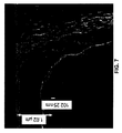
シリコン酸化層9がシリコンホールまたはバイア5中に形成される実験が行われた。これにより、シリコンウエハ1が形成された。シリコンウエハ1は、高いアスペクト比0.1(直径が5μmで深さが50μm)を有するスルーシリコンバイア5を備えて形成された。シリコンウエハ1は、低コンタクト抵抗を実現するために、HF溶液で洗浄された。
An experiment was conducted in which a silicon oxide layer 9 was formed in a silicon hole or via 5. Thereby, the
陽極酸化反応のための電解質溶液として、0.1%のクエン酸溶液が使用された。40Vの陽極酸化電位が印加された。5mA/cm2の電流密度が達成された。陽極酸化が、10時間行われた。膜厚70nmのシリコン酸化層9が得られた。 A 0.1% citric acid solution was used as the electrolyte solution for the anodization reaction. An anodic oxidation potential of 40V was applied. A current density of 5 mA / cm 2 was achieved. Anodization was performed for 10 hours. A silicon oxide layer 9 having a thickness of 70 nm was obtained.
図6から図11は、ホール5の中の結果の酸化層の写真を示す。酸化層が、70nmの膜厚を有した。
6 to 11 show photographs of the resulting oxide layer in
図7は、詳細に示された図6のAを示す。 FIG. 7 shows A of FIG. 6 shown in detail.
図8は、詳細に示された図6のBを示す。 FIG. 8 shows B of FIG. 6 shown in detail.
図9は、ホール5の底を示す。
FIG. 9 shows the bottom of the
図10は、詳細に示された図9のCを示す FIG. 10 shows C of FIG. 9 shown in detail.
図11は、詳細に示された図9のDを示す FIG. 11 shows D of FIG. 9 shown in detail.
それらの写真から、均一に成長した膜厚70nmの酸化層が得られることが分かる。酸化物の膜厚は、高いアスペクト比のホール(5μm幅、50μm深さでアスペクト比0.1)に沿ってすべて均一である。 From these photographs, it can be seen that a uniformly grown oxide layer with a thickness of 70 nm can be obtained. The film thickness of the oxide is all uniform along a high aspect ratio hole (5 μm wide, 50 μm deep and aspect ratio 0.1).
写真から分かるように、連続した等角のシリコン酸化層が、このような高いアスペクト比のバイア5で得られた。 As can be seen from the photograph, a continuous conformal silicon oxide layer was obtained with such high aspect ratio via 5.
本発明にかかるデバイスについて、材料とともに、好適な具体例、特定の構造や形状がここで検討されたが、添付の請求の範囲で規定される本発明の範囲から離れることなく、形状や細部において多くの変形や修正が行えることを理解すべきである。 For the device according to the present invention, together with materials, preferred embodiments, specific structures and shapes have been discussed herein, but in form and detail without departing from the scope of the invention as defined in the appended claims. It should be understood that many variations and modifications can be made.
そのデバイスの製造プロセスが本発明の具体例にかかる方法を含む一例が、図5に示される。この例では、基板1の部分1aは、当業者にSTI領域として良く知られた分離領域を含む。基板1の部分1bは、コンタクト2を形成する複数のバイア1〜バイアnと、複数の金属層M1〜Mn+1とを含む。部分1aと部分1bとの間に、絶縁層3が存在する。この例では、絶縁層3は、第1層3aと第2層3bから形成されても良い。第1層3aは、例えば、例示では、400nmの膜厚のHDPO(高密度プラズマ酸化物)を含む。第2層3bは、例えば、例示では、50nmの膜厚のSiCを含む。図5からわかるように、SiC層3bは、基板1の部分1a中に、少なくとも1つのホールやバイア5をエッチングする場合に、エッチングストップとして働く。本発明の具体例でが、酸化層は、ホールやバイア5中に適用できる。
An example in which the device fabrication process includes a method according to embodiments of the invention is shown in FIG. In this example, the
Claims (6)
分離領域を有するデバイス基板、多層の相互結合構造、およびデバイス基板と多層の相互結合構造との間の絶縁層を含む半導体基板を得る工程と、
デバイス基板の裏側から絶縁層まで、デバイス基板中に含まれる分離領域を通って少なくとも1つのホールをエッチングする工程と、
酸性の電解質溶液中で基板を陽極酸化することにより、基板の上に酸化層を形成する工程と、を含み、
基板の上に酸化層を形成する工程は、
電解質溶液中に基板を浸責する工程と、
電解質溶液中に配置されたカソードと、デバイス基板からなるアノードとの間に10Vと400Vの間の電位を与え、これにより基板を陽極酸化する工程と、で行われ、
陽極酸化する工程は、
最初に、所定の時間、固定された電流密度が、基板を通って得られるように電位を与える工程と、
所定の時間が経過した後に、10Vと400Vの間の固定された電位を与える工程との、2工程のプロセスで行われる方法。 A method of forming an oxide layer on a semiconductor substrate,
Obtaining a semiconductor substrate comprising a device substrate having an isolation region, a multilayer interconnect structure, and an insulating layer between the device substrate and the multilayer interconnect structure;
Etching at least one hole from the back side of the device substrate to the insulating layer through an isolation region included in the device substrate;
Forming an oxide layer on the substrate by anodizing the substrate in an acidic electrolyte solution,
The step of forming an oxide layer on the substrate is as follows:
Immersing the substrate in the electrolyte solution;
Applying a potential between 10 V and 400 V between the cathode disposed in the electrolyte solution and the anode made of the device substrate, thereby anodizing the substrate ,
The process of anodizing
First, applying a potential such that a fixed current density is obtained through the substrate for a predetermined time;
A method performed in a two-step process of applying a fixed potential between 10V and 400V after a predetermined time has elapsed .
Applications Claiming Priority (3)
| Application Number | Priority Date | Filing Date | Title |
|---|---|---|---|
| US5009208P | 2008-05-02 | 2008-05-02 | |
| US61/050,092 | 2008-05-02 | ||
| PCT/EP2009/055312 WO2009133196A1 (en) | 2008-05-02 | 2009-04-30 | Method for providing oxide layers |
Publications (3)
| Publication Number | Publication Date |
|---|---|
| JP2011523202A JP2011523202A (en) | 2011-08-04 |
| JP2011523202A5 JP2011523202A5 (en) | 2012-02-09 |
| JP5528430B2 true JP5528430B2 (en) | 2014-06-25 |
Family
ID=40941299
Family Applications (1)
| Application Number | Title | Priority Date | Filing Date |
|---|---|---|---|
| JP2011506732A Expired - Fee Related JP5528430B2 (en) | 2008-05-02 | 2009-04-30 | Formation method of oxide layer |
Country Status (4)
| Country | Link |
|---|---|
| US (1) | US8822330B2 (en) |
| EP (1) | EP2272087B1 (en) |
| JP (1) | JP5528430B2 (en) |
| WO (1) | WO2009133196A1 (en) |
Families Citing this family (3)
| Publication number | Priority date | Publication date | Assignee | Title |
|---|---|---|---|---|
| US8912522B2 (en) * | 2009-08-26 | 2014-12-16 | University Of Maryland | Nanodevice arrays for electrical energy storage, capture and management and method for their formation |
| US10032569B2 (en) * | 2009-08-26 | 2018-07-24 | University Of Maryland, College Park | Nanodevice arrays for electrical energy storage, capture and management and method for their formation |
| US9219032B2 (en) * | 2012-07-09 | 2015-12-22 | Qualcomm Incorporated | Integrating through substrate vias from wafer backside layers of integrated circuits |
Family Cites Families (16)
| Publication number | Priority date | Publication date | Assignee | Title |
|---|---|---|---|---|
| US4005452A (en) * | 1974-11-15 | 1977-01-25 | International Telephone And Telegraph Corporation | Method for providing electrical isolating material in selected regions of a semiconductive material and the product produced thereby |
| US4849370A (en) * | 1987-12-21 | 1989-07-18 | Texas Instruments Incorporated | Anodizable strain layer for SOI semiconductor structures |
| JP2938152B2 (en) * | 1990-07-06 | 1999-08-23 | 株式会社東芝 | Semiconductor device and manufacturing method thereof |
| JPH06350064A (en) * | 1993-06-07 | 1994-12-22 | Canon Inc | Semiconductor device and packaging method for it |
| US5511428A (en) * | 1994-06-10 | 1996-04-30 | Massachusetts Institute Of Technology | Backside contact of sensor microstructures |
| JP3893645B2 (en) * | 1996-03-18 | 2007-03-14 | ソニー株式会社 | Thin film semiconductor device and IC card manufacturing method |
| JP2815001B2 (en) * | 1996-10-21 | 1998-10-27 | 日本電気株式会社 | Method for manufacturing thin film SOI substrate |
| US5736454A (en) * | 1997-03-20 | 1998-04-07 | National Science Council | Method for making a silicon dioxide layer on a silicon substrate by pure water anodization followed by rapid thermal densification |
| JPH11126906A (en) * | 1997-10-22 | 1999-05-11 | Semiconductor Energy Lab Co Ltd | Anodic oxidation method |
| US6352893B1 (en) * | 1999-06-03 | 2002-03-05 | Infineon Technologies Ag | Low temperature self-aligned collar formation |
| DE10147894B4 (en) * | 2001-07-31 | 2007-08-23 | Infineon Technologies Ag | Method of filling trenches in semiconductor integrated circuits |
| DE10138981B4 (en) * | 2001-08-08 | 2005-09-08 | Infineon Technologies Ag | A method of forming silicon oxide by electrochemical oxidation of a well semiconductor substrate |
| JP4717290B2 (en) * | 2001-09-12 | 2011-07-06 | 株式会社フジクラ | Manufacturing method of through electrode |
| US6815315B2 (en) * | 2002-05-14 | 2004-11-09 | Matsushita Electric Works, Ltd. | Method for electrochemical oxidation |
| JP4035066B2 (en) * | 2003-02-04 | 2008-01-16 | 株式会社ルネサステクノロジ | Manufacturing method of semiconductor device |
| JP4199206B2 (en) * | 2005-03-18 | 2008-12-17 | シャープ株式会社 | Manufacturing method of semiconductor device |
-
2009
- 2009-04-30 WO PCT/EP2009/055312 patent/WO2009133196A1/en active Application Filing
- 2009-04-30 EP EP09738240.2A patent/EP2272087B1/en not_active Not-in-force
- 2009-04-30 JP JP2011506732A patent/JP5528430B2/en not_active Expired - Fee Related
-
2010
- 2010-10-18 US US12/906,766 patent/US8822330B2/en not_active Expired - Fee Related
Also Published As
| Publication number | Publication date |
|---|---|
| JP2011523202A (en) | 2011-08-04 |
| US8822330B2 (en) | 2014-09-02 |
| EP2272087A1 (en) | 2011-01-12 |
| WO2009133196A1 (en) | 2009-11-05 |
| EP2272087B1 (en) | 2018-04-04 |
| US20110086507A1 (en) | 2011-04-14 |
Similar Documents
| Publication | Publication Date | Title |
|---|---|---|
| JP6286780B2 (en) | Electronic devices for radio frequency or power applications and processes for manufacturing such devices | |
| JPS5837987B2 (en) | Method for forming buried oxide isolation regions | |
| US20030008473A1 (en) | Anodizing method and apparatus and semiconductor substrate manufacturing method | |
| EP2458037A1 (en) | A method for precisely controlled masked anodization | |
| TWI374483B (en) | Method for fabricating vertical channel transistor in semiconductor device | |
| JP2004241479A (en) | Method of manufacturing semiconductor device | |
| TW201535593A (en) | Interconnects with fully clad lines | |
| TW200913132A (en) | Method for forming isolation layer in semiconductor device | |
| JP5528430B2 (en) | Formation method of oxide layer | |
| JP4199206B2 (en) | Manufacturing method of semiconductor device | |
| US7659164B1 (en) | Method for fabricating capacitor of semiconductor device | |
| JP2001523050A (en) | Circuit structure having at least one capacitor and method of manufacturing the same | |
| Yan et al. | Facile fabrication of wafer-scale, micro-spacing and high-aspect-ratio silicon microwire arrays | |
| TWI233659B (en) | Method of forming isolation film of semiconductor device | |
| JPH06326077A (en) | Formation method for hole structure in silicon substrate | |
| US20160372336A1 (en) | Method for Manufacturing a Semiconductor Device by Hydrogen Treatment | |
| JP4625216B2 (en) | Low temperature sacrificial oxide formation method | |
| TWI237296B (en) | Semiconductor member and the method for manufacturing the same | |
| TWI250552B (en) | Plating apparatus, plating method, and manufacturing method of semiconductor device | |
| TW583746B (en) | Method of forming a bottle trench | |
| TWI274381B (en) | Method for fabricating semiconductor device and method for fabricating capacitor in a semiconductor device | |
| KR100808595B1 (en) | Method for forming isolation layer of semiconductor device | |
| TW543109B (en) | Formation method of bottle-shaped trench using electrochemical etching | |
| KR100327564B1 (en) | Method for preparing sample used in observation of scanning electron microscope | |
| CN111354676A (en) | Method for forming oxide structure |
Legal Events
| Date | Code | Title | Description |
|---|---|---|---|
| A521 | Written amendment |
Free format text: JAPANESE INTERMEDIATE CODE: A523 Effective date: 20111215 |
|
| A621 | Written request for application examination |
Free format text: JAPANESE INTERMEDIATE CODE: A621 Effective date: 20111215 |
|
| A977 | Report on retrieval |
Free format text: JAPANESE INTERMEDIATE CODE: A971007 Effective date: 20120820 |
|
| A131 | Notification of reasons for refusal |
Free format text: JAPANESE INTERMEDIATE CODE: A131 Effective date: 20120904 |
|
| A521 | Written amendment |
Free format text: JAPANESE INTERMEDIATE CODE: A523 Effective date: 20121204 |
|
| A131 | Notification of reasons for refusal |
Free format text: JAPANESE INTERMEDIATE CODE: A131 Effective date: 20130402 |
|
| A521 | Written amendment |
Free format text: JAPANESE INTERMEDIATE CODE: A523 Effective date: 20130702 |
|
| A02 | Decision of refusal |
Free format text: JAPANESE INTERMEDIATE CODE: A02 Effective date: 20131001 |
|
| A521 | Written amendment |
Free format text: JAPANESE INTERMEDIATE CODE: A523 Effective date: 20140131 |
|
| A911 | Transfer to examiner for re-examination before appeal (zenchi) |
Free format text: JAPANESE INTERMEDIATE CODE: A911 Effective date: 20140207 |
|
| TRDD | Decision of grant or rejection written | ||
| A01 | Written decision to grant a patent or to grant a registration (utility model) |
Free format text: JAPANESE INTERMEDIATE CODE: A01 Effective date: 20140318 |
|
| A61 | First payment of annual fees (during grant procedure) |
Free format text: JAPANESE INTERMEDIATE CODE: A61 Effective date: 20140415 |
|
| R150 | Certificate of patent or registration of utility model |
Ref document number: 5528430 Country of ref document: JP Free format text: JAPANESE INTERMEDIATE CODE: R150 |
|
| R250 | Receipt of annual fees |
Free format text: JAPANESE INTERMEDIATE CODE: R250 |
|
| R250 | Receipt of annual fees |
Free format text: JAPANESE INTERMEDIATE CODE: R250 |
|
| R250 | Receipt of annual fees |
Free format text: JAPANESE INTERMEDIATE CODE: R250 |
|
| R250 | Receipt of annual fees |
Free format text: JAPANESE INTERMEDIATE CODE: R250 |
|
| LAPS | Cancellation because of no payment of annual fees |