EP2247163B1 - Organische lumineszenzanordnung und herstellungsverfahren dafür - Google Patents
Organische lumineszenzanordnung und herstellungsverfahren dafür Download PDFInfo
- Publication number
- EP2247163B1 EP2247163B1 EP09703049.8A EP09703049A EP2247163B1 EP 2247163 B1 EP2247163 B1 EP 2247163B1 EP 09703049 A EP09703049 A EP 09703049A EP 2247163 B1 EP2247163 B1 EP 2247163B1
- Authority
- EP
- European Patent Office
- Prior art keywords
- organic compound
- electrode
- layer
- compound layer
- type organic
- Prior art date
- Legal status (The legal status is an assumption and is not a legal conclusion. Google has not performed a legal analysis and makes no representation as to the accuracy of the status listed.)
- Active
Links
- 238000004519 manufacturing process Methods 0.000 title claims description 13
- 150000002894 organic compounds Chemical class 0.000 claims description 299
- 238000002347 injection Methods 0.000 claims description 84
- 239000007924 injection Substances 0.000 claims description 84
- 238000004768 lowest unoccupied molecular orbital Methods 0.000 claims description 79
- 238000004770 highest occupied molecular orbital Methods 0.000 claims description 77
- 239000011575 calcium Substances 0.000 claims description 67
- 239000000463 material Substances 0.000 claims description 63
- 229910052784 alkaline earth metal Inorganic materials 0.000 claims description 52
- YTVNOVQHSGMMOV-UHFFFAOYSA-N naphthalenetetracarboxylic dianhydride Chemical compound C1=CC(C(=O)OC2=O)=C3C2=CC=C2C(=O)OC(=O)C1=C32 YTVNOVQHSGMMOV-UHFFFAOYSA-N 0.000 claims description 39
- 238000000034 method Methods 0.000 claims description 38
- 239000011777 magnesium Substances 0.000 claims description 30
- 239000011368 organic material Substances 0.000 claims description 30
- 229910052791 calcium Inorganic materials 0.000 claims description 23
- IXHWGNYCZPISET-UHFFFAOYSA-N 2-[4-(dicyanomethylidene)-2,3,5,6-tetrafluorocyclohexa-2,5-dien-1-ylidene]propanedinitrile Chemical compound FC1=C(F)C(=C(C#N)C#N)C(F)=C(F)C1=C(C#N)C#N IXHWGNYCZPISET-UHFFFAOYSA-N 0.000 claims description 20
- CLYVDMAATCIVBF-UHFFFAOYSA-N pigment red 224 Chemical compound C=12C3=CC=C(C(OC4=O)=O)C2=C4C=CC=1C1=CC=C2C(=O)OC(=O)C4=CC=C3C1=C42 CLYVDMAATCIVBF-UHFFFAOYSA-N 0.000 claims description 20
- 229910052749 magnesium Inorganic materials 0.000 claims description 17
- 238000004402 ultra-violet photoelectron spectroscopy Methods 0.000 claims description 17
- 229910052751 metal Inorganic materials 0.000 claims description 16
- 239000002184 metal Substances 0.000 claims description 16
- -1 fluoro-substituted 3,4,9,10-perylenetetracarboxylic Chemical class 0.000 claims description 15
- OYPRJOBELJOOCE-UHFFFAOYSA-N Calcium Chemical compound [Ca] OYPRJOBELJOOCE-UHFFFAOYSA-N 0.000 claims description 12
- FYYHWMGAXLPEAU-UHFFFAOYSA-N Magnesium Chemical compound [Mg] FYYHWMGAXLPEAU-UHFFFAOYSA-N 0.000 claims description 12
- DMEVMYSQZPJFOK-UHFFFAOYSA-N 3,4,5,6,9,10-hexazatetracyclo[12.4.0.02,7.08,13]octadeca-1(18),2(7),3,5,8(13),9,11,14,16-nonaene Chemical group N1=NN=C2C3=CC=CC=C3C3=CC=NN=C3C2=N1 DMEVMYSQZPJFOK-UHFFFAOYSA-N 0.000 claims description 11
- 229920001940 conductive polymer Polymers 0.000 claims description 9
- 230000014509 gene expression Effects 0.000 claims description 9
- 238000002371 ultraviolet--visible spectrum Methods 0.000 claims description 9
- 229910044991 metal oxide Inorganic materials 0.000 claims description 7
- 150000004706 metal oxides Chemical class 0.000 claims description 7
- 239000012780 transparent material Substances 0.000 claims description 5
- 239000010410 layer Substances 0.000 description 550
- 230000032258 transport Effects 0.000 description 82
- 230000005525 hole transport Effects 0.000 description 48
- 239000012044 organic layer Substances 0.000 description 47
- 150000001875 compounds Chemical class 0.000 description 44
- 238000000151 deposition Methods 0.000 description 38
- 230000008021 deposition Effects 0.000 description 37
- 238000010438 heat treatment Methods 0.000 description 37
- 125000003118 aryl group Chemical group 0.000 description 26
- 239000000758 substrate Substances 0.000 description 20
- 229910052782 aluminium Inorganic materials 0.000 description 17
- PQXKHYXIUOZZFA-UHFFFAOYSA-M lithium fluoride Chemical compound [Li+].[F-] PQXKHYXIUOZZFA-UHFFFAOYSA-M 0.000 description 16
- XAGFODPZIPBFFR-UHFFFAOYSA-N aluminium Chemical compound [Al] XAGFODPZIPBFFR-UHFFFAOYSA-N 0.000 description 14
- 230000004888 barrier function Effects 0.000 description 14
- TVIVIEFSHFOWTE-UHFFFAOYSA-K tri(quinolin-8-yloxy)alumane Chemical compound [Al+3].C1=CN=C2C([O-])=CC=CC2=C1.C1=CN=C2C([O-])=CC=CC2=C1.C1=CN=C2C([O-])=CC=CC2=C1 TVIVIEFSHFOWTE-UHFFFAOYSA-K 0.000 description 14
- 229910052737 gold Inorganic materials 0.000 description 13
- 239000010931 gold Substances 0.000 description 13
- 125000004435 hydrogen atom Chemical group [H]* 0.000 description 13
- 125000000217 alkyl group Chemical group 0.000 description 12
- 239000011521 glass Substances 0.000 description 12
- PCHJSUWPFVWCPO-UHFFFAOYSA-N gold Chemical compound [Au] PCHJSUWPFVWCPO-UHFFFAOYSA-N 0.000 description 12
- IJGRMHOSHXDMSA-UHFFFAOYSA-N Atomic nitrogen Chemical compound N#N IJGRMHOSHXDMSA-UHFFFAOYSA-N 0.000 description 10
- 239000010408 film Substances 0.000 description 10
- YVTHLONGBIQYBO-UHFFFAOYSA-N zinc indium(3+) oxygen(2-) Chemical class [O--].[Zn++].[In+3] YVTHLONGBIQYBO-UHFFFAOYSA-N 0.000 description 10
- 125000003545 alkoxy group Chemical group 0.000 description 9
- 239000002019 doping agent Substances 0.000 description 9
- 125000000449 nitro group Chemical group [O-][N+](*)=O 0.000 description 9
- 238000004544 sputter deposition Methods 0.000 description 9
- 239000010406 cathode material Substances 0.000 description 8
- 230000000052 comparative effect Effects 0.000 description 8
- 125000000753 cycloalkyl group Chemical group 0.000 description 8
- 229910052717 sulfur Inorganic materials 0.000 description 8
- 125000002947 alkylene group Chemical group 0.000 description 7
- 125000003277 amino group Chemical group 0.000 description 7
- 125000005843 halogen group Chemical group 0.000 description 7
- 229910052760 oxygen Inorganic materials 0.000 description 7
- 229910052709 silver Inorganic materials 0.000 description 7
- 125000003342 alkenyl group Chemical group 0.000 description 6
- RTZKZFJDLAIYFH-UHFFFAOYSA-N ether Substances CCOCC RTZKZFJDLAIYFH-UHFFFAOYSA-N 0.000 description 6
- 125000001072 heteroaryl group Chemical group 0.000 description 6
- 230000006872 improvement Effects 0.000 description 6
- 125000003710 aryl alkyl group Chemical group 0.000 description 5
- 125000004429 atom Chemical group 0.000 description 5
- 125000004432 carbon atom Chemical group C* 0.000 description 5
- 230000007423 decrease Effects 0.000 description 5
- 230000000694 effects Effects 0.000 description 5
- 125000005842 heteroatom Chemical group 0.000 description 5
- 150000002739 metals Chemical class 0.000 description 5
- PXHVJJICTQNCMI-UHFFFAOYSA-N nickel Substances [Ni] PXHVJJICTQNCMI-UHFFFAOYSA-N 0.000 description 5
- 125000002560 nitrile group Chemical group 0.000 description 5
- 229910052757 nitrogen Inorganic materials 0.000 description 5
- 238000005424 photoluminescence Methods 0.000 description 5
- 239000010409 thin film Substances 0.000 description 5
- XEEYBQQBJWHFJM-UHFFFAOYSA-N Iron Chemical compound [Fe] XEEYBQQBJWHFJM-UHFFFAOYSA-N 0.000 description 4
- 125000001931 aliphatic group Chemical group 0.000 description 4
- 239000010405 anode material Substances 0.000 description 4
- 125000005013 aryl ether group Chemical group 0.000 description 4
- 125000000732 arylene group Chemical group 0.000 description 4
- 230000008859 change Effects 0.000 description 4
- 239000004020 conductor Substances 0.000 description 4
- 125000004093 cyano group Chemical group *C#N 0.000 description 4
- ZUOUZKKEUPVFJK-UHFFFAOYSA-N diphenyl Chemical compound C1=CC=CC=C1C1=CC=CC=C1 ZUOUZKKEUPVFJK-UHFFFAOYSA-N 0.000 description 4
- 239000007772 electrode material Substances 0.000 description 4
- 229910052736 halogen Inorganic materials 0.000 description 4
- 150000002367 halogens Chemical class 0.000 description 4
- 125000000623 heterocyclic group Chemical group 0.000 description 4
- 125000000592 heterocycloalkyl group Chemical group 0.000 description 4
- 229910052739 hydrogen Inorganic materials 0.000 description 4
- 239000001257 hydrogen Substances 0.000 description 4
- 125000002971 oxazolyl group Chemical group 0.000 description 4
- 125000004430 oxygen atom Chemical group O* 0.000 description 4
- 125000004434 sulfur atom Chemical group 0.000 description 4
- 238000002207 thermal evaporation Methods 0.000 description 4
- WHXSMMKQMYFTQS-UHFFFAOYSA-N Lithium Chemical compound [Li] WHXSMMKQMYFTQS-UHFFFAOYSA-N 0.000 description 3
- BQCADISMDOOEFD-UHFFFAOYSA-N Silver Chemical compound [Ag] BQCADISMDOOEFD-UHFFFAOYSA-N 0.000 description 3
- QVGXLLKOCUKJST-UHFFFAOYSA-N atomic oxygen Chemical compound [O] QVGXLLKOCUKJST-UHFFFAOYSA-N 0.000 description 3
- 125000003178 carboxy group Chemical group [H]OC(*)=O 0.000 description 3
- 125000002883 imidazolyl group Chemical group 0.000 description 3
- 229910052744 lithium Inorganic materials 0.000 description 3
- 229910052750 molybdenum Inorganic materials 0.000 description 3
- 229910052759 nickel Inorganic materials 0.000 description 3
- 239000001301 oxygen Substances 0.000 description 3
- 125000004076 pyridyl group Chemical group 0.000 description 3
- 125000005493 quinolyl group Chemical group 0.000 description 3
- 238000002310 reflectometry Methods 0.000 description 3
- 239000004065 semiconductor Substances 0.000 description 3
- 239000004332 silver Substances 0.000 description 3
- 125000001424 substituent group Chemical group 0.000 description 3
- 125000003903 2-propenyl group Chemical group [H]C([*])([H])C([H])=C([H])[H] 0.000 description 2
- UJOBWOGCFQCDNV-UHFFFAOYSA-N 9H-carbazole Chemical compound C1=CC=C2C3=CC=CC=C3NC2=C1 UJOBWOGCFQCDNV-UHFFFAOYSA-N 0.000 description 2
- DGAQECJNVWCQMB-PUAWFVPOSA-M Ilexoside XXIX Chemical compound C[C@@H]1CC[C@@]2(CC[C@@]3(C(=CC[C@H]4[C@]3(CC[C@@H]5[C@@]4(CC[C@@H](C5(C)C)OS(=O)(=O)[O-])C)C)[C@@H]2[C@]1(C)O)C)C(=O)O[C@H]6[C@@H]([C@H]([C@@H]([C@H](O6)CO)O)O)O.[Na+] DGAQECJNVWCQMB-PUAWFVPOSA-M 0.000 description 2
- SIKJAQJRHWYJAI-UHFFFAOYSA-N Indole Chemical group C1=CC=C2NC=CC2=C1 SIKJAQJRHWYJAI-UHFFFAOYSA-N 0.000 description 2
- ZOKXTWBITQBERF-UHFFFAOYSA-N Molybdenum Chemical compound [Mo] ZOKXTWBITQBERF-UHFFFAOYSA-N 0.000 description 2
- 229910003813 NRa Inorganic materials 0.000 description 2
- ZLMJMSJWJFRBEC-UHFFFAOYSA-N Potassium Chemical compound [K] ZLMJMSJWJFRBEC-UHFFFAOYSA-N 0.000 description 2
- FZWLAAWBMGSTSO-UHFFFAOYSA-N Thiazole Chemical group C1=CSC=N1 FZWLAAWBMGSTSO-UHFFFAOYSA-N 0.000 description 2
- XLOMVQKBTHCTTD-UHFFFAOYSA-N Zinc monoxide Chemical compound [Zn]=O XLOMVQKBTHCTTD-UHFFFAOYSA-N 0.000 description 2
- DGEZNRSVGBDHLK-UHFFFAOYSA-N [1,10]phenanthroline Chemical group C1=CN=C2C3=NC=CC=C3C=CC2=C1 DGEZNRSVGBDHLK-UHFFFAOYSA-N 0.000 description 2
- 238000010521 absorption reaction Methods 0.000 description 2
- 125000003172 aldehyde group Chemical group 0.000 description 2
- 150000001338 aliphatic hydrocarbons Chemical class 0.000 description 2
- 125000004414 alkyl thio group Chemical group 0.000 description 2
- 239000000956 alloy Substances 0.000 description 2
- 229910045601 alloy Inorganic materials 0.000 description 2
- MWPLVEDNUUSJAV-UHFFFAOYSA-N anthracene Chemical compound C1=CC=CC2=CC3=CC=CC=C3C=C21 MWPLVEDNUUSJAV-UHFFFAOYSA-N 0.000 description 2
- 150000004832 aryl thioethers Chemical group 0.000 description 2
- 125000001797 benzyl group Chemical group [H]C1=C([H])C([H])=C(C([H])=C1[H])C([H])([H])* 0.000 description 2
- 235000010290 biphenyl Nutrition 0.000 description 2
- 239000004305 biphenyl Substances 0.000 description 2
- 125000003917 carbamoyl group Chemical group [H]N([H])C(*)=O 0.000 description 2
- 125000000609 carbazolyl group Chemical group C1(=CC=CC=2C3=CC=CC=C3NC12)* 0.000 description 2
- 125000002915 carbonyl group Chemical group [*:2]C([*:1])=O 0.000 description 2
- 229910052802 copper Inorganic materials 0.000 description 2
- 239000010949 copper Substances 0.000 description 2
- 125000000392 cycloalkenyl group Chemical group 0.000 description 2
- 125000000596 cyclohexenyl group Chemical group C1(=CCCCC1)* 0.000 description 2
- 125000000113 cyclohexyl group Chemical group [H]C1([H])C([H])([H])C([H])([H])C([H])(*)C([H])([H])C1([H])[H] 0.000 description 2
- 125000000058 cyclopentadienyl group Chemical group C1(=CC=CC1)* 0.000 description 2
- 238000009826 distribution Methods 0.000 description 2
- 230000005684 electric field Effects 0.000 description 2
- ZSWFCLXCOIISFI-UHFFFAOYSA-N endo-cyclopentadiene Natural products C1C=CC=C1 ZSWFCLXCOIISFI-UHFFFAOYSA-N 0.000 description 2
- 125000004185 ester group Chemical group 0.000 description 2
- 125000001495 ethyl group Chemical group [H]C([H])([H])C([H])([H])* 0.000 description 2
- 125000000524 functional group Chemical group 0.000 description 2
- 125000002541 furyl group Chemical group 0.000 description 2
- 125000002887 hydroxy group Chemical group [H]O* 0.000 description 2
- 229910052738 indium Inorganic materials 0.000 description 2
- APFVFJFRJDLVQX-UHFFFAOYSA-N indium atom Chemical compound [In] APFVFJFRJDLVQX-UHFFFAOYSA-N 0.000 description 2
- 229910052742 iron Inorganic materials 0.000 description 2
- 238000005259 measurement Methods 0.000 description 2
- 125000000956 methoxy group Chemical group [H]C([H])([H])O* 0.000 description 2
- 125000002496 methyl group Chemical group [H]C([H])([H])* 0.000 description 2
- 239000000203 mixture Substances 0.000 description 2
- 239000011733 molybdenum Substances 0.000 description 2
- 125000001624 naphthyl group Chemical group 0.000 description 2
- 125000002868 norbornyl group Chemical group C12(CCC(CC1)C2)* 0.000 description 2
- 125000000951 phenoxy group Chemical group [H]C1=C([H])C([H])=C(O*)C([H])=C1[H] 0.000 description 2
- 125000001997 phenyl group Chemical group [H]C1=C([H])C([H])=C(*)C([H])=C1[H] 0.000 description 2
- 229920000553 poly(phenylenevinylene) Polymers 0.000 description 2
- 229920000642 polymer Polymers 0.000 description 2
- 229910052700 potassium Inorganic materials 0.000 description 2
- 239000011591 potassium Substances 0.000 description 2
- 125000002943 quinolinyl group Chemical group N1=C(C=CC2=CC=CC=C12)* 0.000 description 2
- 229910052710 silicon Inorganic materials 0.000 description 2
- 239000010703 silicon Substances 0.000 description 2
- 150000003967 siloles Chemical class 0.000 description 2
- 125000005401 siloxanyl group Chemical group 0.000 description 2
- 125000003808 silyl group Chemical group [H][Si]([H])([H])[*] 0.000 description 2
- 229910052708 sodium Inorganic materials 0.000 description 2
- 239000011734 sodium Substances 0.000 description 2
- 239000000243 solution Substances 0.000 description 2
- 125000001544 thienyl group Chemical group 0.000 description 2
- XOLBLPGZBRYERU-UHFFFAOYSA-N tin dioxide Chemical compound O=[Sn]=O XOLBLPGZBRYERU-UHFFFAOYSA-N 0.000 description 2
- PWYVVBKROXXHEB-UHFFFAOYSA-M trimethyl-[3-(1-methyl-2,3,4,5-tetraphenylsilol-1-yl)propyl]azanium;iodide Chemical compound [I-].C[N+](C)(C)CCC[Si]1(C)C(C=2C=CC=CC=2)=C(C=2C=CC=CC=2)C(C=2C=CC=CC=2)=C1C1=CC=CC=C1 PWYVVBKROXXHEB-UHFFFAOYSA-M 0.000 description 2
- 125000000026 trimethylsilyl group Chemical group [H]C([H])([H])[Si]([*])(C([H])([H])[H])C([H])([H])[H] 0.000 description 2
- 125000000391 vinyl group Chemical group [H]C([*])=C([H])[H] 0.000 description 2
- 229920002554 vinyl polymer Polymers 0.000 description 2
- 235000014692 zinc oxide Nutrition 0.000 description 2
- BCMCBBGGLRIHSE-UHFFFAOYSA-N 1,3-benzoxazole Chemical compound C1=CC=C2OC=NC2=C1 BCMCBBGGLRIHSE-UHFFFAOYSA-N 0.000 description 1
- HYZJCKYKOHLVJF-UHFFFAOYSA-N 1H-benzimidazole Chemical compound C1=CC=C2NC=NC2=C1 HYZJCKYKOHLVJF-UHFFFAOYSA-N 0.000 description 1
- 239000005725 8-Hydroxyquinoline Substances 0.000 description 1
- OKTJSMMVPCPJKN-UHFFFAOYSA-N Carbon Chemical compound [C] OKTJSMMVPCPJKN-UHFFFAOYSA-N 0.000 description 1
- VYZAMTAEIAYCRO-UHFFFAOYSA-N Chromium Chemical compound [Cr] VYZAMTAEIAYCRO-UHFFFAOYSA-N 0.000 description 1
- RYGMFSIKBFXOCR-UHFFFAOYSA-N Copper Chemical compound [Cu] RYGMFSIKBFXOCR-UHFFFAOYSA-N 0.000 description 1
- 229910052688 Gadolinium Inorganic materials 0.000 description 1
- UFHFLCQGNIYNRP-UHFFFAOYSA-N Hydrogen Chemical compound [H][H] UFHFLCQGNIYNRP-UHFFFAOYSA-N 0.000 description 1
- ATJFFYVFTNAWJD-UHFFFAOYSA-N Tin Chemical compound [Sn] ATJFFYVFTNAWJD-UHFFFAOYSA-N 0.000 description 1
- RTAQQCXQSZGOHL-UHFFFAOYSA-N Titanium Chemical compound [Ti] RTAQQCXQSZGOHL-UHFFFAOYSA-N 0.000 description 1
- HCHKCACWOHOZIP-UHFFFAOYSA-N Zinc Chemical compound [Zn] HCHKCACWOHOZIP-UHFFFAOYSA-N 0.000 description 1
- QCWXUUIWCKQGHC-UHFFFAOYSA-N Zirconium Chemical compound [Zr] QCWXUUIWCKQGHC-UHFFFAOYSA-N 0.000 description 1
- 230000002411 adverse Effects 0.000 description 1
- 125000004453 alkoxycarbonyl group Chemical group 0.000 description 1
- 150000004982 aromatic amines Chemical class 0.000 description 1
- 125000005110 aryl thio group Chemical group 0.000 description 1
- 125000004104 aryloxy group Chemical group 0.000 description 1
- 230000008901 benefit Effects 0.000 description 1
- IOJUPLGTWVMSFF-UHFFFAOYSA-N benzothiazole Chemical compound C1=CC=C2SC=NC2=C1 IOJUPLGTWVMSFF-UHFFFAOYSA-N 0.000 description 1
- 229910052790 beryllium Inorganic materials 0.000 description 1
- ATBAMAFKBVZNFJ-UHFFFAOYSA-N beryllium atom Chemical compound [Be] ATBAMAFKBVZNFJ-UHFFFAOYSA-N 0.000 description 1
- UFVXQDWNSAGPHN-UHFFFAOYSA-K bis[(2-methylquinolin-8-yl)oxy]-(4-phenylphenoxy)alumane Chemical compound [Al+3].C1=CC=C([O-])C2=NC(C)=CC=C21.C1=CC=C([O-])C2=NC(C)=CC=C21.C1=CC([O-])=CC=C1C1=CC=CC=C1 UFVXQDWNSAGPHN-UHFFFAOYSA-K 0.000 description 1
- 229920001400 block copolymer Polymers 0.000 description 1
- 229910052792 caesium Inorganic materials 0.000 description 1
- TVFDJXOCXUVLDH-UHFFFAOYSA-N caesium atom Chemical compound [Cs] TVFDJXOCXUVLDH-UHFFFAOYSA-N 0.000 description 1
- 229910052799 carbon Inorganic materials 0.000 description 1
- 239000002800 charge carrier Substances 0.000 description 1
- 229910052804 chromium Inorganic materials 0.000 description 1
- 239000011651 chromium Substances 0.000 description 1
- 230000005494 condensation Effects 0.000 description 1
- 238000009833 condensation Methods 0.000 description 1
- 239000002181 crystalline organic material Substances 0.000 description 1
- 125000005567 fluorenylene group Chemical group 0.000 description 1
- 239000003574 free electron Substances 0.000 description 1
- UIWYJDYFSGRHKR-UHFFFAOYSA-N gadolinium atom Chemical compound [Gd] UIWYJDYFSGRHKR-UHFFFAOYSA-N 0.000 description 1
- 150000002430 hydrocarbons Chemical group 0.000 description 1
- 229910003437 indium oxide Inorganic materials 0.000 description 1
- PJXISJQVUVHSOJ-UHFFFAOYSA-N indium(iii) oxide Chemical class [O-2].[O-2].[O-2].[In+3].[In+3] PJXISJQVUVHSOJ-UHFFFAOYSA-N 0.000 description 1
- AMGQUBHHOARCQH-UHFFFAOYSA-N indium;oxotin Chemical class [In].[Sn]=O AMGQUBHHOARCQH-UHFFFAOYSA-N 0.000 description 1
- 229910010272 inorganic material Inorganic materials 0.000 description 1
- 239000011147 inorganic material Substances 0.000 description 1
- 239000011133 lead Substances 0.000 description 1
- 150000004767 nitrides Chemical class 0.000 description 1
- 229960003540 oxyquinoline Drugs 0.000 description 1
- 238000002186 photoelectron spectrum Methods 0.000 description 1
- 229920002098 polyfluorene Polymers 0.000 description 1
- 230000008569 process Effects 0.000 description 1
- MCJGNVYPOGVAJF-UHFFFAOYSA-N quinolin-8-ol Chemical compound C1=CN=C2C(O)=CC=CC2=C1 MCJGNVYPOGVAJF-UHFFFAOYSA-N 0.000 description 1
- 239000010944 silver (metal) Substances 0.000 description 1
- 238000001228 spectrum Methods 0.000 description 1
- 150000003413 spiro compounds Chemical class 0.000 description 1
- 239000000126 substance Substances 0.000 description 1
- 229910052715 tantalum Inorganic materials 0.000 description 1
- GUVRBAGPIYLISA-UHFFFAOYSA-N tantalum atom Chemical compound [Ta] GUVRBAGPIYLISA-UHFFFAOYSA-N 0.000 description 1
- 239000011135 tin Substances 0.000 description 1
- 229910052718 tin Inorganic materials 0.000 description 1
- 229910001887 tin oxide Inorganic materials 0.000 description 1
- QHGNHLZPVBIIPX-UHFFFAOYSA-N tin(ii) oxide Chemical class [Sn]=O QHGNHLZPVBIIPX-UHFFFAOYSA-N 0.000 description 1
- 229910052719 titanium Inorganic materials 0.000 description 1
- 239000010936 titanium Substances 0.000 description 1
- WFKWXMTUELFFGS-UHFFFAOYSA-N tungsten Chemical compound [W] WFKWXMTUELFFGS-UHFFFAOYSA-N 0.000 description 1
- 229910052721 tungsten Inorganic materials 0.000 description 1
- 239000010937 tungsten Substances 0.000 description 1
- 229910052720 vanadium Inorganic materials 0.000 description 1
- GPPXJZIENCGNKB-UHFFFAOYSA-N vanadium Chemical compound [V]#[V] GPPXJZIENCGNKB-UHFFFAOYSA-N 0.000 description 1
- 229910052725 zinc Inorganic materials 0.000 description 1
- 239000011701 zinc Substances 0.000 description 1
- 239000011787 zinc oxide Substances 0.000 description 1
- RNWHGQJWIACOKP-UHFFFAOYSA-N zinc;oxygen(2-) Chemical class [O-2].[Zn+2] RNWHGQJWIACOKP-UHFFFAOYSA-N 0.000 description 1
- 229910052726 zirconium Inorganic materials 0.000 description 1
Images


Classifications
-
- H—ELECTRICITY
- H05—ELECTRIC TECHNIQUES NOT OTHERWISE PROVIDED FOR
- H05B—ELECTRIC HEATING; ELECTRIC LIGHT SOURCES NOT OTHERWISE PROVIDED FOR; CIRCUIT ARRANGEMENTS FOR ELECTRIC LIGHT SOURCES, IN GENERAL
- H05B33/00—Electroluminescent light sources
- H05B33/12—Light sources with substantially two-dimensional radiating surfaces
- H05B33/14—Light sources with substantially two-dimensional radiating surfaces characterised by the chemical or physical composition or the arrangement of the electroluminescent material, or by the simultaneous addition of the electroluminescent material in or onto the light source
-
- C—CHEMISTRY; METALLURGY
- C09—DYES; PAINTS; POLISHES; NATURAL RESINS; ADHESIVES; COMPOSITIONS NOT OTHERWISE PROVIDED FOR; APPLICATIONS OF MATERIALS NOT OTHERWISE PROVIDED FOR
- C09K—MATERIALS FOR MISCELLANEOUS APPLICATIONS, NOT PROVIDED FOR ELSEWHERE
- C09K11/00—Luminescent, e.g. electroluminescent, chemiluminescent materials
- C09K11/06—Luminescent, e.g. electroluminescent, chemiluminescent materials containing organic luminescent materials
-
- H—ELECTRICITY
- H05—ELECTRIC TECHNIQUES NOT OTHERWISE PROVIDED FOR
- H05B—ELECTRIC HEATING; ELECTRIC LIGHT SOURCES NOT OTHERWISE PROVIDED FOR; CIRCUIT ARRANGEMENTS FOR ELECTRIC LIGHT SOURCES, IN GENERAL
- H05B33/00—Electroluminescent light sources
- H05B33/12—Light sources with substantially two-dimensional radiating surfaces
- H05B33/18—Light sources with substantially two-dimensional radiating surfaces characterised by the nature or concentration of the activator
-
- H—ELECTRICITY
- H10—SEMICONDUCTOR DEVICES; ELECTRIC SOLID-STATE DEVICES NOT OTHERWISE PROVIDED FOR
- H10K—ORGANIC ELECTRIC SOLID-STATE DEVICES
- H10K50/00—Organic light-emitting devices
-
- H—ELECTRICITY
- H10—SEMICONDUCTOR DEVICES; ELECTRIC SOLID-STATE DEVICES NOT OTHERWISE PROVIDED FOR
- H10K—ORGANIC ELECTRIC SOLID-STATE DEVICES
- H10K50/00—Organic light-emitting devices
- H10K50/10—OLEDs or polymer light-emitting diodes [PLED]
- H10K50/11—OLEDs or polymer light-emitting diodes [PLED] characterised by the electroluminescent [EL] layers
-
- H—ELECTRICITY
- H10—SEMICONDUCTOR DEVICES; ELECTRIC SOLID-STATE DEVICES NOT OTHERWISE PROVIDED FOR
- H10K—ORGANIC ELECTRIC SOLID-STATE DEVICES
- H10K50/00—Organic light-emitting devices
- H10K50/10—OLEDs or polymer light-emitting diodes [PLED]
- H10K50/14—Carrier transporting layers
- H10K50/16—Electron transporting layers
- H10K50/165—Electron transporting layers comprising dopants
-
- H—ELECTRICITY
- H10—SEMICONDUCTOR DEVICES; ELECTRIC SOLID-STATE DEVICES NOT OTHERWISE PROVIDED FOR
- H10K—ORGANIC ELECTRIC SOLID-STATE DEVICES
- H10K50/00—Organic light-emitting devices
- H10K50/10—OLEDs or polymer light-emitting diodes [PLED]
- H10K50/14—Carrier transporting layers
- H10K50/16—Electron transporting layers
- H10K50/167—Electron transporting layers between the light-emitting layer and the anode
-
- H—ELECTRICITY
- H10—SEMICONDUCTOR DEVICES; ELECTRIC SOLID-STATE DEVICES NOT OTHERWISE PROVIDED FOR
- H10K—ORGANIC ELECTRIC SOLID-STATE DEVICES
- H10K50/00—Organic light-emitting devices
- H10K50/10—OLEDs or polymer light-emitting diodes [PLED]
- H10K50/17—Carrier injection layers
- H10K50/171—Electron injection layers
-
- C—CHEMISTRY; METALLURGY
- C09—DYES; PAINTS; POLISHES; NATURAL RESINS; ADHESIVES; COMPOSITIONS NOT OTHERWISE PROVIDED FOR; APPLICATIONS OF MATERIALS NOT OTHERWISE PROVIDED FOR
- C09K—MATERIALS FOR MISCELLANEOUS APPLICATIONS, NOT PROVIDED FOR ELSEWHERE
- C09K2211/00—Chemical nature of organic luminescent or tenebrescent compounds
- C09K2211/10—Non-macromolecular compounds
- C09K2211/1018—Heterocyclic compounds
- C09K2211/1025—Heterocyclic compounds characterised by ligands
- C09K2211/1029—Heterocyclic compounds characterised by ligands containing one nitrogen atom as the heteroatom
- C09K2211/1033—Heterocyclic compounds characterised by ligands containing one nitrogen atom as the heteroatom with oxygen
-
- C—CHEMISTRY; METALLURGY
- C09—DYES; PAINTS; POLISHES; NATURAL RESINS; ADHESIVES; COMPOSITIONS NOT OTHERWISE PROVIDED FOR; APPLICATIONS OF MATERIALS NOT OTHERWISE PROVIDED FOR
- C09K—MATERIALS FOR MISCELLANEOUS APPLICATIONS, NOT PROVIDED FOR ELSEWHERE
- C09K2211/00—Chemical nature of organic luminescent or tenebrescent compounds
- C09K2211/10—Non-macromolecular compounds
- C09K2211/1018—Heterocyclic compounds
- C09K2211/1025—Heterocyclic compounds characterised by ligands
- C09K2211/1029—Heterocyclic compounds characterised by ligands containing one nitrogen atom as the heteroatom
- C09K2211/1037—Heterocyclic compounds characterised by ligands containing one nitrogen atom as the heteroatom with sulfur
-
- H—ELECTRICITY
- H10—SEMICONDUCTOR DEVICES; ELECTRIC SOLID-STATE DEVICES NOT OTHERWISE PROVIDED FOR
- H10K—ORGANIC ELECTRIC SOLID-STATE DEVICES
- H10K2101/00—Properties of the organic materials covered by group H10K85/00
- H10K2101/30—Highest occupied molecular orbital [HOMO], lowest unoccupied molecular orbital [LUMO] or Fermi energy values
-
- H—ELECTRICITY
- H10—SEMICONDUCTOR DEVICES; ELECTRIC SOLID-STATE DEVICES NOT OTHERWISE PROVIDED FOR
- H10K—ORGANIC ELECTRIC SOLID-STATE DEVICES
- H10K2101/00—Properties of the organic materials covered by group H10K85/00
- H10K2101/40—Interrelation of parameters between multiple constituent active layers or sublayers, e.g. HOMO values in adjacent layers
Definitions
- the present invention relates to an organic light emitting device that has a low energy barrier for charge injection from an electrode to an organic compound layer, a low driving voltage, and high efficiency and luminance, and to a method for manufacturing the organic light emitting device.
- an organic light emitting device includes two electrodes and an organic compound layer interposed between the electrodes.
- electrons and holes are injected into the organic compound layer from the two electrodes, and a current is converted into visible light.
- an electron/hole injection layer or an electron/hole transport layer may be further provided, in addition to the organic compound layer for converting the current into visible light.
- an interface between the electrode formed of metal, metal oxides, or conductive polymers and the organic compound layer is unstable. Accordingly, heat applied from the outside, internally generated heat, or an electric field applied to the device has an adverse effect on performance of the device. Further, a driving voltage for device operation may be increased due to a difference in conductive energy level between the electron/hole injection layer or the electron/hole transport layer and another organic compound layer adjacent thereto. Accordingly, it is important to stabilize an interface between the electron/hole injection layer or the electron/hole transport layer and another organic compound layer. It is also important to make injection of electrons/holes easy by minimizing an energy barrier for injection of electrons/holes from the electrode to the organic compound layers.
- the organic light emitting device has been developed so as to adjust a difference of energy level between two or more electrodes and an organic compound layer interposed between the electrodes.
- an anode is adjusted to have a Fermi energy level similar to an HOMO (highest occupied molecular orbital) energy level of a hole injection layer or a material having an HOMO energy level similar to a Fermi energy level of an anode is selected for a hole injection layer.
- HOMO highest occupied molecular orbital
- a material having an HOMO energy level similar to a Fermi energy level of an anode is selected for a hole injection layer.
- the hole injection layer needs to be selected in view of an HOMO energy level of a hole transport layer or a light emitting layer close to the hole injection layer as well as in view of the Fermi energy level of the anode, there is a limitation to select a material for the hole injection layer.
- a method of adjusting a Fermi energy level of an electrode is adopted.
- Materials for an anode are limited to materials having a high Fermi energy level of 5.0 ⁇ 5.5 eV, for example ITO, IZO, Au, Ni, Mo and the like, because materials having an HOMO level of about 5.0 ⁇ 5.5 eV are generally used as an organic compound layer that are adjacent to the anode.
- Materials for a cathode are also selected to have a proper Fermi energy level depending on an LUMO energy level of an electron transport layer that transports electrons.
- An electron transport layer generally has LUMO level of about 3.0 eV, and thus materials having a Fermi energy level less than 3.0 eV are preferably used for cathode materials.
- materials for a cathode include lithium (Li), calcium (Ca), magnesium (Mg) and the like.
- metals having a relatively high Fermi energy level such as aluminum (Al), silver (Ag) and the like are used for a cathode, while an electron injection layer between an electrode and an electron transport layer is used in order to improve injection of electrons.
- Materials such as LiF, NaF, KF and the like can be used for the electron injection layer and the above materials are known to reduce the energy barrier for electron injection to an electron transport layer.
- Electrode materials are limited to being used as anode materials or cathode materials depending on their Fermi energy level in order to improve charge injection into organic compounds. While transparent electrode materials having a high Fermi energy level such as ITO, IZO and the like can be used as anode materials, materials having a low Fermi energy level and a high reflectivity such as Al, Ag and the like can be used as cathode materials. Due to the limitation in the selection of electron materials, most of organic light emitting devices have a structure in which light is emitted through a transparent anode. Recently, it is required to emit light through a cathode, and thus anode materials having a high reflectivity and cathode materials having a high transparency are required.
- cathode materials having an excellent transparency has increased.
- Materials that have a low Fermi energy level and a semi-transparent property when they are deposited into a thin film such as Mg, Ag, MgAg, Ca, CaAg and the like are used as transparent cathode materials.
- the semi-transparent cathode materials have a problem in that their conductivity decreases because electrodes have to be formed with thin films in order to improve their transparency.
- WO 2007/011132 relates to an organic light emitting device and a method for manufacturing the same.
- the organic light emitting device includes a first electrode, one or more organic compound layers, and a second electrode.
- the first electrode includes a conductive layer and an n-type organic compound layer disposed on the conductive layer.
- a difference in energy between an LUMO energy level of the n-type organic compound layer of the first electrode and a Fermi energy level of the conductive layer of the first electrode is 4 eV or less.
- One of the organic compound layers interposed between the n-type organic compound layer of the first electrode and the second electrode is a p-type organic compound layer forming an NP junction along with the n-type organic compound layer of the first electrode.
- a difference in energy between the LUMO energy level of the n-type organic compound layer of the first electrode and an HOMO energy level of the p-type organic compound layer is 1 eV or less.
- One or more layers interposed between the conductive layer of the first electrode and the second electrode is n-doped or p-doped with an organic material or an inorganic material.
- the present invention has been finalized in view of the drawbacks inherent in the related art, and it is an object of the present invention to provide an organic light emitting device having a simplified manufacturing process and an excellent performance that reduces an energy barrier for charge injection from an electrode to an organic compound, thus reducing a driving voltage, and can use various electrode materials as an anode and a cathode without any limitation.
- a first aspect of the present invention concerns an organic light emitting device comprising a first electrode, two or more organic compound layers, and a second electrode, wherein the first electrode comprises a conductive layer and an n-type organic compound layer which is in contact with the conductive layer, one of the organic compound layers interposed between the n-type organic compound layer of the first electrode and the second electrode is a p-type organic compound layer forming an NP junction together with the n-type organic compound layer of the first electrode, energy levels of the layers satisfy the following Expressions (1) and (2), and one or more layers interposed between the p-type organic compound layer and the second electrode are n-doped with alkali earth metal: 0 eV ⁇ E nL - E Fl ⁇ 4 eV E pH - E nL ⁇ 1 eV where E F1 is a Fermi level of the conductive layer of the first electrode, E nL is an LUMO (lowest unoccupied molecular orbital) energy level of the n-type organic compound
- a second aspect of the invention concerns a method for manufacturing an organic light emitting device, which comprises a first electrode, two or more organic compound layers, and a second electrode, wherein the method comprises, in this order, forming an n-type organic compound layer on a conductive layer such that the n-type organic compound layer is in contact with the conductive layer so as to form a first electrode, forming a p-type organic compound layer on the n-type organic compound layer of the first electrode such that the p-type organic compound layer is in contact with the n-type organic compound layer, forming an organic compound layer n-doped with alkali earth metal over the p-type organic compound layer, and forming a second electrode on the organic compound layer n-doped with alkali earth metal such that the second electrode is in contact with the organic compound layer n-doped with alkali earth metal, wherein energy levels of the layers satisfy the following Expressions (1) and (2): 0 eV ⁇ E nL - E Fl ⁇ 4 eV
- a third aspect of the invention concerns a method for manufacturing an organic light emitting device, which comprises a second electrode, two or more organic compound layers, and a first electrode, wherein the method comprises, in this order, forming a second electrode, forming an organic compound layer n-doped with alkali earth metal on the second electrode such that the n-doped organic compound layer is in contact with the second electrode, forming a p-type organic compound layer over the n-doped organic compound layer, forming an n-type organic compound layer on the p-type organic compound layer such that the n-type organic compound layer is in contact with the p-type organic compound layer, and forming a conductive layer on the n-type organic compound layer such that the conductive layer is in contact with the n-type organic compound layer so as to form a first electrode, wherein energy levels of the layers satisfy the following Expressions (1) and (2): 0 eV ⁇ E nL - E Fl ⁇ 4 eV E pH - E nL ⁇
- the organic light emitting device of the first aspect is a stacked organic light emitting device comprising two or more repeating units, wherein each of the repeating units comprises a first electrode, two or more organic compound layers, and a second electrode as defined for the first aspect, wherein the second electrode of one repeating unit is connected to the first electrode of another repeating unit that is connected in series to the one repeating unit.
- the organic light emitting device of the first aspect is a stacked organic light emitting device comprising a first electrode, a second electrode, two or more emitting units interposed between the first electrode and the second electrode, and an intermediate electrode interposed between the emitting units, wherein the first electrode comprises a conductive layer and an n-type organic compound layer which is in contact with the conductive layer, the intermediate electrode comprises a conductive layer and an n-type organic compound layer which is in contact with the conductive layer, each of the emitting units comprises a p-type organic compound layer forming an NP junction together with the n-type organic compound layer of the first electrode or the intermediate electrode, energy levels of the layers satisfy the following Expressions (1) and (2), and each of the emitting units further comprises an organic compound layer n-doped with alkali earth metal: 0 eV ⁇ E nL - E Fl ⁇ 4 eV E pH - E nL ⁇ 1 eV where E F1 is a Fermi level
- the organic light emitting device has a low energy barrier for charge injection and an excellent charge transport ability of a charge transport organic compound layer so as to have excellent device performances, such as efficiency, luminance, or a driving voltage. Further, since various materials can be used as a material for an electrode, a device manufacturing process can be simplified. In addition, since the anode and the cathode can be formed of the same material, a stacked organic light emitting device having a high luminance can be obtained. Since an electrode made of ITO, IZO and the like having a high Fermi energy level can be used as a cathode and an intermediate electrode, an organic light emitting device having a high luminance can be manufactured. Further, since the transparent ITO and IZO electrodes can be used as both an anode and a cathode, a transparent organic light emitting device can be manufactured.
- An organic light emitting device comprises a first electrode, a second electrode, and an organic compound layer having p-type semiconductor characteristics (hereinafter, simply referred to as "p-type organic compound layer") interposed between the first electrode and the second electrode.
- the p-type organic compound layer includes a hole injection layer, a hole transport layer or a light emitting layer.
- the organic light emitting device is characterized in that at least one organic compound layer between the p-type organic compound layer and the second electrode is further included and one or more of the organic compound layers are n-doped with alkali earth metal.
- the organic compound layers may be formed of the same material or different materials.
- the first electrode comprises a conductive layer and an organic compound layer having n-type semiconductor characteristics (hereinafter, simply referred to as "n-type organic compound layer") that is in contact with the conductive layer. Since the conductive layer is in contact with the n-type organic compound layer, materials more various than conventional electrode materials can be used for the conductive layer. For example, metal, metal oxides, or conductive polymers can be used as materials of the conductive layer.
- the conductive polymer may include electrical conductive polymer.
- the conductive layer of the first electrode may be formed of the same material as the second electrode.
- the n-type organic compound layer has a predetermined LUMO energy level with respect to a Fermi energy level of the conductive layer and an HOMO energy level of the p-type organic compound layer.
- the n-type organic compound layer of the first electrode is selected such that a difference in energy between the LUMO energy level of the n-type organic compound layer of the first electrode and the Fermi energy level of the conductive layer of the first electrode and a difference in energy between the LUMO energy level of the n-type organic compound layer and the HOMO energy level of the p-type organic compound layer are reduced. Accordingly, holes are easily injected into the HOMO energy level of the p-type organic compound layer through the LUMO energy level of the n-type organic compound layer of the first electrode.
- the difference in energy between the LUMO energy level of the n-type organic compound layer of the first electrode and the Fermi energy level of the conductive layer of the first electrode is preferably more than 0 eV and 4 eV or less. In view of material selection, more preferably, the difference in energy is in a range of about 0.01 to 4 eV.
- the difference in energy between the LUMO energy level of the n-type organic compound layer of the first electrode and the HOMO energy level of the p-type organic compound layer is preferably 1 eV or less, and more preferably, is about 0.5 eV or less (not including 0 eV). In view of material selection, the difference is preferably in a range of -1 eV to 1 eV, and more preferably in a range of about 0.01 to 1 eV.
- the difference in energy between the LUMO energy level of the n-type organic compound layer of the first electrode and the Fermi energy level of the conductive layer of the first electrode is larger than 4 eV, an effect of a surface dipole or a gap state on an energy barrier for hole injection is reduced. If the difference in energy between the LUMO energy level of the n-type organic compound layer and the HOMO energy level of the p-type organic compound layer is larger than 1 eV, an NP junction between the p-type organic compound layer and the n-type organic compound layer of the first electrode does not easily occur, which causes an increase in driving voltage for hole injection. That is, in the present invention, the NP junction has to satisfy the above energy relationship as well as the condition that the n-type organic compound layer is in contact with the p-type organic compound layer.
- a Fermi energy level of the conductive layer, an LUMO level of the n-type organic compound layer and an HOMO level of the p-type organic compound layer that is forming interface with the n-type organic compound layer play very important roles.
- a conventional organic light emitting device used a method in which holes are directly injected from an anode to an HOMO level of an organic compound layer.
- an n-type organic compound layer having a high LUMO level is included in an electrode, an n-type organic compound and a p-type organic compound form the NP junction, and thus the NP junction causes charge generation.
- charges are transported through LUMO level of the n-type organic compound layer between an n-type organic compound layer and the conductive layer that are used as an electrode.
- an HOMO level of the p-type organic compound is larger than an LUMO level of the n-type organic compound so that electrons on the HOMO level of the p-type organic compound can move spontaneously to the empty LUMO level of the n-type organic compound by energy difference.
- holes generate at the HOMO level of the p-type organic compound and electrons generate at the LUMO level of the n-type organic compound.
- This is a principle of charge generation. Charges do not spontaneously generate at the opposed energy level. At this time, in order to generate charges, a vacuum level is required to change by dipoles at the interface and the like.
- vacuum level (VL) can change in approximately 1 eV at the NP interface by the influence of dipoles
- an HOMO level of the p-type organic compound is limited having the energy level 1 eV or more higher than an LUMO level of the n-type organic compound as the condition to spontaneously generate charges.
- a Fermi level of the conductive layer and an LUMO level of the n-type organic compound have to be energy levels that can make electrons at an n-type LUMO level between electrons and holes to be generated at the NP junction move into the conductive layer.
- charges can move by dipole generation, gap state or change of the vacuum level (VL) according to the movement of free electrons in the conductive layer to the LUMO level of the n-type organic compound at the interface of the conductive layer and the n-type organic layer.
- the condition that the LUMO level of the n-type organic compound has to be 4 eV larger than the Fermi level of the conductive layer is deduced by experimental results of the organic light emitting device using a Ca conductive layer (Fermi level 2.6 eV) and an n-type organic compound HAT (LUMO level ⁇ 5.7 V).
- FIGS. 1(a) and (b) show the energy level of the first electrode before and after application of the n-type organic compound layer to the first electrode for hole injection in the organic light emitting device according to the illustrative embodiment of the present invention.
- the conductive layer has a Fermi energy level E F1 lower than a LUMO energy level F nL of the n-type organic compound layer.
- a vacuum level (VL) represents an energy level at which electrons are deprived from the conductive layer and the n-type organic compound layer to air.
- the conductive layer comes into contact with the n-type organic compound layer.
- the Fermi energy levels E F1 and E F2 of the two layers are made equal to each other. Consequently, the surface dipole is formed at the interface of the conductive layer and the n-type organic layer, and the vacuum level, the Fermi energy level, the HOMO energy level, and the LUMO energy level are changed as shown in FIG. 1(b) .
- the energy barrier for hole injection can be reduced by bringing the conductive layer into contact with the n-type organic compound layer. Further, when the conductive layer has a Fermi energy level lower than the LUMO energy level of the n-type organic compound layer, electrons move from the conductive layer to the n-type organic compound layer, and a gap state is formed at an interface between the conductive layer and the n-type organic compound layer. Therefore, the energy barrier for electron transport is minimized.
- the n-type organic compound layer is formed of a material selected from 2,3,5,6-tetrafluoro-7,7,8,8-tetracyanoquinodimethane (F4TCNQ), fluoro-substituted 3,4,9,10-perylenetetracarboxylic dianhydride (PTCDA), cyano-substituted PTCDA, naphthalene-tetracaboxylic-dianhydride (NTCDA), fluoro-substituted NTCDA, cyano-substituted NTCDA, or hexanitrile hexaazatriphenylene (HAT), which has an LUMO energy level of about 5.24 eV.
- F4TCNQ 2,3,5,6-tetrafluoro-7,7,8,8-tetracyanoquinodimethane
- PTCDA fluoro-substituted 3,4,9,10-perylenetetracarboxylic dianhydride
- the organic light emitting device includes a p-type organic compound layer that comes into contact with the n-type organic compound layer of the first electrode for hole injection. Accordingly, the NP junction is formed in the device.
- FIG. 2 shows an NP junction formed between the n-type organic compound layer of the first electrode and the p-type organic compound layer.
- the NP junction When the NP junction is formed, the difference in energy level between the LUMO energy level of the n-type organic compound layer of the first electrode and the HOMO energy level of the p-type organic compound layer is reduced. Accordingly, holes or electrons are easily formed by an external voltage or light source. That is, with the NP junction, holes are easily formed in the p-type organic compound layer, and electrons are easily formed in the n-type organic compound layer of the first electrode. Since the holes and electrons are simultaneously formed in the NP junction, the electrons are transported to the conductive layer of the first electrode through the n-type organic compound layer of the first electrode, and the holes are transported to the p-type organic compound layer.
- the difference in energy level between the LUMO energy level of the n-type organic compound layer of the first electrode and the HOMO energy level of the p-type organic compound layer needs to be a predetermined level. That is, the difference between the LUMO energy level of the n-type organic compound layer of the first electrode and the HOMO energy level of the p-type organic compound layer is preferably about 1 eV or less, and more preferably, is about 0.5 eV or less.
- the p-type organic compound layer may be a hole injection layer, a hole transport layer or a light emitting layer.
- the organic light emitting device can comprise at least one organic compound layers between the p-type organic compound layer and the organic compound layer n-doped with alkali earth metal or between the organic compound layer n-doped with alkali earth metal and the second electrode.
- one or more layers of the organic compound layers interposed between the p-type organic compound layer and the second electrode are characterized in being n-doped with alkali earth metal.
- a density of charge carriers in the organic compound layer increases by the organic compound layer n-doped with alkali earth metal, thereby improving charge transport efficiency in the device and a driving voltage can be reduced by minimizing energy barrier to an electrode.
- a stacked organic light emitting device having high efficiency and transparency can be manufactured because a cathode having a high Fermi energy level can be used.
- the n-doped organic compound layer is preferably an electron injection layer, an electron transport layer or an electron injection and transport layer.
- the organic compound layer n-doped with alkali earth metal is preferably contact with the second electrode.
- the energy barrier for hole injection from the first electrode to the organic compound layer can be significantly reduced. Accordingly, hole injection and transport from the first electrode to a light emitting region of the organic light emitting device can be efficiently performed.
- the organic light emitting device according to the present invention having a high hole injection efficiency as describing above, when an organic compound layer interposed between the p-type organic compound layer and the second electrode, for example, the organic compound layer for electron injection and/or transport is n-doped with alkali earth metal thereby improving electron transport ability, electrons as well as holes may reach the light emitting region of the device at high concentration.
- the organic light emitting device according to the present invention can achieve balancing at emitting region.
- the term "balancing" means that the density of holes and the density of electrons that contribute to light-emission are maximized and they are the same as each other.
- the organic light emitting device according to the present invention can exhibit excellent low voltage, high luminance, and high efficiency characteristics.
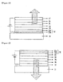
- FIG. 16 is a schematic view showing the transport of holes and electrons in the organic light emitting device wherein only the NP junction between the NP junction and the n-type doped organic compound layer is applied.
- the organic light emitting device wherein only the NP junction between the NP junction and the n-type doped organic compound layer is applied, only the injection property and transport property of holes can be improved so that the concentration of holes in a light emitting layer becomes relatively higher than that of electrons, thereby reducing balancing of holes and electrons.
- a driving voltage reduces by the improvement of injection property and transport property of holes, but a photoluminescence also reduces. Therefore, a light-emitting efficiency represented by Watt ratio is formulated as current times voltage against photoluminescence and it cannot be expected to increase.
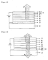
- FIG. 17 is a schematic view showing the transport of holes and electrons in the organic light emitting device wherein only the n-type doped organic compound layer between the NP junction and the n-type doped organic compound layer is applied.
- the organic light emitting device wherein only the n-type doped organic compound layer between the NP junction and the n-type doped organic compound layer is applied, only the injection property and transport property of electrons can be improved so that the concentration of electrons in a light emitting layer becomes relatively higher than that of holes, thereby reducing balancing of holes and electrons.
- a driving voltage reduces by the improvement of injection property and transport property of electrons, but a photoluminescence also reduces. Therefore, a light-emitting efficiency represented by Watt ratio is formulated as current times voltage against photoluminescence and it cannot be expected to increase.
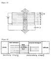
- FIG. 18 is a schematic view showing the transport of holes and electrons in the organic light emitting device wherein both the NP junction and the n-type doped organic compound layer are applied.
- both the NP junction and the n-type doped organic compound layer are used, both the improvement of holes injection and transport properties by the NP junction and the improvement of electrons injection and transport properties by the n-doping can be achieved.
- the concentration of electrons and holes in a light emitting layer achieve balancing so that a driving voltage is largely reduced by the improvement of injection property and transport property of charges and s luminance is improved by balancing of electrons and holes. Therefore, an organic light emitting device in which a light-emitting efficiency represented by Watt ratio that is expressed as current times voltage to photoluminescence is high can be manufactured.
- the alkali earth metal doped into the organic compound layer include one or more selected from the group consisting of calcium (Ca), and magnesium (Mg).
- Electron injection or transport materials can be used as the material of the organic compound layer n-doped with alkali earth metal, but it is not limited thereto.
- the compound having the functional group selected from the group consisting of an imidazole group, an oxazole group, a thiazole group, a quinoline group and a phenanthroline group can be used.
- Preferred examples of the compound having the functional group that is selected from the group consisting of the imidazole group, the oxazole group, and the thiazole group include a compound that is represented by the following Formula 1 or 2.
- R 1 to R 4 may be the same or different from each other, are each independently a hydrogen atom; a C 1 to C 30 alkyl group that is unsubstituted or substituted with one or more groups selected from the group consisting of a halogen atom, an amino group, a nitrile group, a nitro group, a C 1 to C 30 alkyl group, a C 2 to C 30 alkenyl group, a C 1 to C 30 alkoxy group, a C 3 to C 30 cycloalkyl group, a C 3 to C 30 heterocycloalkyl group, a C 5 to C 30 aryl group, and a C 2 to C 30 heteroaryl group; a C 3 to C 30 cycloalkyl group that is unsubstituted or substituted with one or more groups selected from the group consisting of a halogen atom, an amino group, a nitrile group, a nitro group, a C 1 to C 30 alkyl group
- X is O, S, NR b or a C 1 to C 7 divalent hydrocarbon group
- A, D, and R b are each a hydrogen atom, a nitrile group (-CN), a nitro group (-NO 2 ), a C 1 to C 24 alkyl, a C 5 to C 20 aromatic ring or a hetero-atom substituted aromatic ring, a halogen, or an alkylene or an alkylene containing a hetero-atom that can form a fused ring in conjunction with an adjacent ring
- a and D may be connected to each other to form an aromatic or hetero aromatic ring
- B is a linkage unit and substituted or unsubstituted alkylene or arylene that conjugately or unconjugately connects multiple hetero rings when n is 2 or more, and substituted or unsubstituted alkyl or aryl when n is 1; and n is an integer in the range of 1 to 8.
- Examples of the compound that is represented by the above Formula 1 and used as the compound applied to the above organic substance layer include a compound that is disclosed in Korean Patent Application Publication No. 2003-0067773 , and examples of the compound that is represented by the above Formula 2 include a compound that is disclosed in US Pat. No. 5,645,948 and a compound that is disclosed in WO05/097756 The disclosures of above-mentioned documents are incorporated herein by reference in its entirety.
- the compound that is represented by the above Formula 1 includes the compound that is represented by the following Formula 3.
- R 5 to R 7 are the same or different from each other, are each independently a hydrogen atom, a C 1 to C 20 aliphatic hydrocarbon, an aromatic ring, an aromatic hetero ring or an aliphatic or aromatic fused ring; Ar is a direct bond, an aromatic ring, an aromatic hetero ring or an aliphatic or aromatic fused ring; and X is O, S, or NR a , R a is a hydrogen atom, a C 1 to C 7 aliphatic hydrocarbon, an aromatic ring, or an aromatic hetero ring, with a proviso that R 5 and R 6 can not simultaneously be hydrogen.
- the compound that is represented by the above Formula 2 includes the compound that is represented by the following Formula 4.
- Z is O, S, or NR b
- R 8 and R b are a hydrogen atom, a C 1 to C 24 alkyl, a C 5 to C 20 aromatic ring or a hetero-atom substituted aromatic ring, a halogen, or an alkylene or an alkylene containing a hetero-atom that can form a fused ring in conjunction with a benzazole ring:
- B is a linkage unit and alkylene, arylene, substituted alkylene, or substituted arylene that conjugately or unconjugately connects multiple benzazoles when n is 2 or more and substituted or unsubstituted alkyl or aryl when n is 1, and n is an integer in the range of 1 to 8.
- Examples of the preferable compound having an imidazole group include compounds having the following structures.
- examples of the compound having the quinoline group include compounds that are represented by the following Formulae 5 to 11.
- n is an integer in the range of 0 to 9
- m is an integer in the range of 2 or more
- R 9 is one selected from the group consisting of hydrogen, an alkyl group such as methyl and ethyl, a cycloalkyl group such as cyclohexyl and a norbornyl, an aralkyl group such as benzyl group, an alkenyl group such as vinyl and allyl, a cycloalkenyl group such as cyclopentadienyl and cyclohexenyl, an alkoxy group such as methoxy, an alkylthio group in which an oxygen atom in ether bonding of an alkoxy group is substituted by a sulfur atom, an arylether group such as phenoxy, an arylthioether group in which an oxygen atom in ether bonding of an arylether group is
- examples of the compound having a phenanthroline group include compounds that are represented by the following Formulae 12 to 22. wherein m is an integer of 1 or more, n and p are integers, n+p is 8 or less, when m is 1, R 10 and R 11 are each one selected from the group consisting of hydrogen, an alkyl group such as methyl and ethyl, a cycloalkyl group such as cyclohexyl and a norbornyl, an aralkyl group such as benzyl group, an alkenyl group such as vinyl and allyl, a cycloalkenyl group such as cyclopentadienyl and cyclohexenyl, an alkoxy group such as methoxy, an alkylthio group in which an oxygen atom in ether bonding of an alkoxy group is substituted by a sulfur atom, an arylether group such as phenoxy, an arylthioether group in which an oxygen atom in
- R 1a to R 8a and R 1b to R 10b are independently selected from the group consisting of a hydrogen atom, a substituted or unsubstituted aryl group having 5-60 nuclear atoms, a substituted or unsubstituted pyridyl group, a substituted or unsubstituted quinolyl group, a substituted or unsubstituted alkyl group having 1-50 carbon atoms, a substituted or unsubstituted cycloalkyl group having 3-50 carbon atoms, a substituted or unsubstituted aralkyl group having 6-50 nuclear atoms, a substituted or unsubstituted alkoxy group having 1-50 carbon atoms, a substituted or unsubstituted aryloxy group having 5-50 nuclear atoms, a substituted or unsubstituted arylthio group having 5-50 nuclear atoms, a substituted or unsubstituted alk
- d 1 , d 3 to d 10 and g 1 are independently selected from the group consisting of a hydrogen atom and an aromatic or aliphatic hydrocarbon group, m and n are integers of 0 to 2, p is an integer of 0 to 3.
- the compounds of Formulae 20 and 21 are disclosed in U.S. Patent Application Publication No. 2007/0122656 , the disclosures of which are incorporated herein by reference in its entirety.
- R 1c to R 6c are independently selected from the group consisting of a hydrogen atom, a substituted or unsubstituted alkyl group, a substituted or unsubstituted aralkyl group, a substituted or unsubstituted aryl group, a substituted or unsubstituted heterocyclic group and a halogen atom
- Ar 1c and Ar 2c are independently selected from the following formulae: wherein R 17 to R 23 are independently selected from the group consisting of a hydrogen atom, a substituted or unsubstituted alkyl group, a substituted or unsubstituted aralkyl group, a substituted or unsubstituted aryl group, a substituted or unsubstituted heterocyclic group and a halogen atom.
- the compound of Foumula 22 is disclosed in Japanese Patent Application Publication No. 2004-107263 , the disclosures of which are incorporated herein by reference in its entirety.
- the organic compound layer n-doped with alkali earth metal can be formed by a known method in the art, but the scope of the present invention is not limited to a specific method.
- the doping concentration in the organic compound layer n-doped with alkali earth metal is efficiently 0.02 to 50 volume% in terms of improvement of electrons injection efficiency.
- the organic compound layer n-doped with alkali earth metal may be an electron injection layer, an electron transport layer or electron transport and injection layer.
- the organic light emitting device according to the present invention may further comprise at least one organic compound layers between the p-type organic compound layer and the organic compound layer n-doped with alkali earth metal or between the organic compound layer n-doped with alkali earth metal and the second electrode.
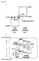
- FIG. 3 illustrates the organic light emitting device according to an embodiment of the invention.
- the organic light emitting device may include a substrate 31, an anode 32 on the substrate 31, a p-type hole injection layer (HIL) 33 that is formed on the anode 32 and accepts holes from the anode 32, a hole transport layer (HTL) 34 that is formed on the hole injection layer 33 and transports the holes to an emitting layer (EML) 35, the emitting layer 35 that is formed on the hole transport layer 34 and emits light using the holes and electrons, an electron transport layer (ETL) 36 that is formed on the emitting layer 35 and transports the electrons from a cathode 37 to the emitting layer 35, and the cathode 37 that is formed on the electron transport layer 36.
- the hole transport layer 34, the emitting layer 35, and the electron transport layer 36 may be formed of the same organic material or different organic materials.
- the anode 32 transports the holes to the hole injection layer 33, the hole transport layer 34, or the emitting layer 35, and includes a conductive layer 32a and an n-type organic layer 32b.
- the conductive layer 32a is formed of metal, metal oxides, or conductive polymers.
- a difference in energy between an LUMO energy level of the n-type organic layer 32b and a Fermi energy level of the conductive layer 32a is about 4 eV or less.
- a difference in energy between the LUMO energy level of the n-type organic layer 32b and an HOMO energy level of the p-type hole injection layer 33 is about 1 eV or less, and preferably about 0.5 eV or less.
- An NP junction is formed between the n-type organic layer 32b of the anode 32 and the p-type hole injection layer 33.
- the organic light emitting device may include a substrate 31, an anode 32 that is formed on the substrate 31, a p-type hole transport layer 34 that is formed on the anode 32, an emitting layer 35 that is formed on the hole transport layer 34, an electron transport layer 36 that is formed on the emitting layer 35, and a cathode 37 that is formed on the electron transport layer 36.
- the emitting layer 35 and the electron transport layer 36 may be formed of the same organic material or different organic materials.
- the organic light emitting device may include a substrate 31, an anode 32 that is formed on the substrate 31, a p-type emitting layer 35 that is formed on the anode 32, an electron transport layer 36 that is formed on the emitting layer 35, and a cathode 37 that is formed on the electron transport layer 36.
- the electron transport layer 36 may be formed of organic material.
- a difference in energy between the LUMO energy level of the n-type organic layer 32b and the HOMO energy level of the p-type hole transport layer 34 or the emitting layer 35 is about 1 eV or less, and preferably about 0.5 eV or less.
- An NP junction is formed between the n-type organic layer 32b of the anode 32 and the p-type hole transport layer 34 or the p-type emitting layer 35.
- the difference in energy between the LUMO energy level of the n-type organic layer 32b and the Fenni energy level of the conductive layer 32a is more than 4 eV, a surface dipole or gap state effect to an energy barrier for injection of the holes into the p-type hole injection layer 33 is reduced. If the difference in energy between the LUMO energy level of the n-type organic layer 32b and the HOMO energy level of the p-type hole injection layer 33 is more than 1 eV, the holes or the electrons are not easily formed from the p-type hole injection layer 33 or the n-type organic layer 32b, and driving voltage for injection of the holes is increased.
- FIG. 3 shows an embodiment where a first electrode comprising a conductive layer and an n-type organic compound layer, an organic compound layer and a second electrode are sequentially layered on a substrate.
- the present invention comprises an inverted structure where a second electrode, an organic compound layer and a first electrode comprising a conductive layer and an n-type organic compound layer are sequentially layered on a substrate.
- FIG. 4 illustrates ideal energy level of the known organic light emitting device. At the energy level, loss of energy for injection of the holes and the electrons from the anode and the cathode is minimized.
- FIG. 5 illustrates energy level of the organic light emitting device according to the embodiment of the invention.
- the organic light emitting device includes the anode having the conductive layer and the n-type organic layer (see FIG. 3 ), the p-type hole injection layer (HIL), the hole transport layer (HTL), the emitting layer (EML), the electron transport layer (ETL), and the cathode.
- the difference in energy between the LUMO energy level of the n-type organic layer of the anode and the Fermi energy level of the conductive layer of the anode is about 4 eV or less, and the difference in energy between the LUMO energy level of the n-type organic layer of the anode and the HOMO energy level of the p-type hole injection layer is about 1 eV or less.
- the holes are easily transported from the anode to the emitting layer using the LUMO energy level of the n-type organic layer of the anode and the HOMO energy level of the p-type hole injection layer.
- FIGs 9 to 15 show the organic light emitting devices according to the illustrative embodiment of the present invention.
- the conductive layer of the anode may be formed of various conductive materials.
- the conductive layer may be formed of the same material as the cathode.
- the organic light emitting device where conductive material has a low work function may be produced.
- the subject invention can achieve the balancing of holes and electrons by improving the transport properties of holes and electrons by the above technical constitutions. Therefore, even though an electron injection layer made of materials such as LiF is not included, the present invention can achieve the device performance higher than that of an organic light emitting device having an electron injection layer such as a LiF layer. At this time, the organic compound layer n-doped with alkali earth metal may be contact with the second electrode. However, the present invention does not exclude to comprise an electron injection layer from the scope.
- the present invention can provide with a stacked organic light emitting device having a high efficiency and a high luminance by the above described principle.
- a luminance increases in proportion to the number of stacked organic light emitting device units under the same driving voltage. Therefore, an organic light emitting device having high a luminance can be manufactured when the organic light emitting device is a stacked type.
- Another aspect of the present invention provides a stacked organic light emitting device comprising two or more repeating units, wherein each of the repeating units comprises a first electrode, two or more organic compound layers, and a second electrode, as defined above wherein the second electrode of one repeating unit is connected to the first electrode of another repeating unit that is connected in series to the one repeating unit.
- FIG. 6 shows a stacked organic light emitting device according to one embodiment of the present invention.
- an anode (71) comprises a conductive layer and an n-type organic compound layer.
- Another aspect of the present invention provides the above-defined organic light emitting device in the form of a stacked organic light emitting device comprising a first electrode, a second electrode, two or more emitting units interposed between the first electrode and the second electrode, and an intermediate electrode interposed between the emitting units, wherein the first electrode comprises a conductive layer and an n-type organic compound layer which is in contact with the conductive layer, the intermediate electrode comprises a conductive layer and an n-type organic compound layer which is in contact with the conductive layer, each of the emitting units comprises a p-type organic compound layer forming an NP junction together with the n-type organic compound layer of the first electrode or the intermediate electrode, energy levels of the layers satisfy the following Expressions (1) and (2), and each of the emitting units further comprises an organic compound layer n-doped with alkali earth metal: 0 eV ⁇ E nL - E Fl ⁇ 4 eV E pH - E nL ⁇ 1 eV where E F1 is a Fermi
- the cathode and the anode may be formed of the same material, a stacked organic light emitting device in FIG. 7 that is equivalent to the structure shown in FIG. 6 may be produced.
- the stacked organic light emitting device according to the invention has a structure where a plurality of repeating units of an organic layer 83 and an intermediate electrode conductive layer 85 interposed between an anode 81 and a cathode 87 are layered.
- the anode 81 and the intermediate electrode layer 85 comprise a conductive layer and an n-type organic layer.
- the conductive layer is formed of the transparent material that has a work function similar to that of the cathode 87 and visible ray transmissivity of 50% or more.
- opaque metal is used as the material of the conductive layer, it is necessary for the conductive layer to be made thin so that the conductive layer is transparent.
- the opaque metal may include Al, Ag, Cu, Ca, Mg, MgAg, CaAg, etc.
- Al metal forms the conductive layer of the intermediate electrode layer 85
- the conductive layer has a thickness of about 5 to 10 nm, but it is not limited thereto.
- the conductive layer that is included in the intermediate electrode may be a very thin film, for example having 5 ⁇ to 1,000 ⁇ , more preferably 10 ⁇ to 900 ⁇ .
- layers constituting the organic light emitting device according to the embodiment of the invention will be described in detail.
- the layers as described below may be formed of the single material or a mixture of two or more materials.
- the anode injects the holes into the p-type organic layer, such as the hole injection layer, the hole transport layer, or the emitting layer.
- the anode includes the conductive layer and the n-type organic layer.
- the conductive layer includes metal, metal oxides, or conductive polymers.
- the conductive polymers may include electroconductive polymers.
- the conductive layer may be formed of various conductive materials.
- the conductive layer has a Fermi energy level of about 2 to 5.5 eV.
- materials having a Fermi energy level of 5 to 6 eV are used for an anode.
- materials having a Fermi energy level of 2 to 5 eV, particularly materials having a Fermi energy level of 2 to 4 eV can be used for an anode.
- the conductive material examples include carbon, cesium, potassium, lithium, calcium, sodium, magnesium, zirconium, indium, aluminum, silver, tantalum, vanadium, chromium, copper, zinc, iron, tungsten, molybdenum, nickel, gold, other metals, and alloys thereof; zinc oxides, indium oxides, tin oxides, indium tin oxides (ITO), indium zinc oxides, and metal oxides that are similar thereto; and mixtures of oxides and metals, such as ZnO:Al and SnO 2 :Sb.
- opaque material having excellent reflectivity as well as transparent material may be used as the material of the conductive layer.
- transparent material In the case of a bottom emission type of organic light emitting device, transparent material must be used as the material of the conductive layer. If opaque material is used, the layer must be made thin so that the layer is almost transparent. In order to adjust a Fermi energy level of the conductive layer, the surface of the conductive layer may be treated with nitrogen plasma or oxygen plasma.
- the Fermi energy level of the conductive layer that is treated with plasma increases by oxygen plasma and it decreases by nitrogen plasma.
- nitrogen plasma increases the conductivity of the conductive layer, reduces the concentration of oxygen on the surface, and generates nitrides on the surface, thus increasing life span of the device.
- nitrogen plasma may reduce a Fermi energy level of the conductive layer so that the injection of holes deteriorates, thus increasing a driving voltage.
- the holes injection property due to the NP junction is not influenced even though a Fermi energy level of the conductive layer decreases. Therefore, in the present invention, nitrogen plasma is practical, and thus a device having long life span and low voltage can be realized.
- the n-type organic layer is interposed between the conductive layer and the p-type organic layer, and injects the holes into the p-type organic layer in a low electric field.
- the n-type organic layer is selected so that a difference in energy between an LUMO energy level of the n-type organic layer of the anode and a Fermi energy level of the conductive layer of the anode is about 4 eV or less and a difference in energy between the LUMO energy level of the n-type organic layer and an HOMO energy level of the p-type organic layer is about 1 eV or less.
- the n-type organic layer has the LUMO energy level of about 4 to 7 eV and electron mobility of about 10 -8 cm 2 /Vs to 1 cm 2 /Vs, and preferably 10 -6 cm 2 /Vs to 10 -2 cm 2 /Vs. If the electron mobility is less than 10 -8 cm 2 /Vs, it is not easy to inject the holes from the n-type organic layer to the p-type organic layer. If the electron mobility is more than 1 cm 2 /Vs, the injection of the holes is effectively performed. However, in this case, since the layer is typically formed of crystalline organic material, it is difficult to apply the layer to the organic light emitting device using noncrystalline organic material.
- the n-type organic layer may be formed of material that is capable of being vacuum deposited or used to form a thin film using a solution process.
- the n-type organic material is selected from 2,3,5,6-tetrafluoro-7,7,8,8-tetracyanoquinodimethane (F4TCNQ), fluorine-substituted 3,4,9,10-perylenetetracarboxylic dianhydride (PTCDA), cyano-substituted PTCDA, naphthalenetetracarboxylic dianhydride (NTCDA), fluorine-substituted NTCDA, cyano-substituted NTCDA, or hexanitrile hexaazatriphenylene (HAT).
- F4TCNQ 2,3,5,6-tetrafluoro-7,7,8,8-tetracyanoquinodimethane
- PTCDA fluorine-substituted 3,4,9,10-perylenet
- HIL Hole injection layer
- HTL hole transport layer
- the hole injection layer or the hole transport layer may be formed of the p-type organic layer interposed between the anode and the cathode. Since the p-type hole injection layer or the p-type hole transport layer and the n-type organic layer form an NP junction, the holes formed due to the NP junction are transported through the p-type hole injection layer or the p-type hole transport layer to the emitting layer.
- the difference in energy between the HOMO energy level of the p-type hole injection layer or the p-type hole transport layer and the LUMO energy level of the n-type organic layer is about 1 eV or less, and preferably about 0.5 eV or less.
- Examples of the p-type hole injection layer or the p-type hole transport layer include, but are not limited to arylamine-based compounds, conductive polymers, or block copolymers having both a conjugated portion and an unconjugated portion.
- Emitting layer EML
- the emitting layer may have both n-type and p-type charactertistics.
- the emitting layer may be defined as the n-type emitting layer in case the electron transportation is faster than the hole transportation, and also defined as the p-type emitting layer in case the hole transportation is faster than the electron transportation.
- the n-type emitting layer since the electron transportation is faster than the hole transportation, light emission occurs at the interface between the hole transport layer and the emitting layer. Accordingly, if the LUMO energy level of the hole transport layer is higher than the LUMO energy level of the emitting layer, higher light emission efficiency may be assured.
- the n-type emitting layer include, but are not limited to aluminum tris(8-hydroxyquinoline) (Alq 3 ); 8-hydroxyquinoline beryllium (BAlq); a benzoxazole-based compound, a benzthiazol-based compound, or a benzimidazole-based compound; a polyfluorene-based compound; and a silacyclopentadiene (silole)-based compound.
- hole transport is rapider than electron transport, and thus light emission is made in the vicinity of an interface between the electron transport layer and the light emitting layer. Accordingly, if the HOMO energy level of the electron transport layer is lower than the HOMO energy level of the light emitting layer, higher light emission efficiency can be obtained.
- an increase effect of light emission efficiency by a change in LUMO energy level of the hole transport layer is smaller as compared to the case where an n-type light emitting layer is used. Accordingly, in case of using the p-type light emitting layer, it is possible to manufacture an organic light emitting device having an NP junction structure between the n-type organic compound layer and the p-type light emitting layer, without using a hole injection layer and a hole transport layer.
- the p-type light emitting layer includes, but not limited to, a carbazole-based compound, an anthracene-based compound, a polyphenylenevinylene (PPV)-based polymer, or a spiro compound.
- ETL Electron Transport Layer
- the electron transport layer As a material for the electron transport layer, a material having large electron mobility so as to receive electrons from a cathode and transport the electrons to the light emitting layer is preferably used.
- the electron transport layer includes, but are not limited to aluminum tris-(8-hydroxyquinoline) (Alq 3 ), an organic compound comprising Alq 3 structure, or a hydroxy flavone-metal complex compound or a silacyclopentadiene (silole)-based compound.
- a material having a low work function in order to easily inject electrons into the organic compound layer such as an electron transport layer
- materials having work function (Fermi level) of 6.0 eV or less can be used for a cathode.
- the cathode includes, but not limited to, a metal, such as magnesium, calcium, sodium, potassium, titanium, indium, yittrium, lithium, gadolinium, aluminum, silver, tin, nickel, gold, molybdenum, iron and lead or an alloy thereof; a multilayered material, such as LiF/Al or LiO 2 /Al; and a metal oxide such as ITO, IZO and the like.
- a metal such as magnesium, calcium, sodium, potassium, titanium, indium, yittrium, lithium, gadolinium, aluminum, silver, tin, nickel, gold, molybdenum, iron and lead or an alloy thereof
- a multilayered material such as LiF/Al or LiO 2 /Al
- a metal oxide such as ITO, IZO and the like.
- the cathode can be formed of the same material to the conductive layer of the anode.
- the cathode or the conductive layer of the anode may include a transparent
- Hexanitrile hexaazatriphenylene was used as the organic material having n-type semiconductor characteristics.
- a UPS Ultraviolet photoelectron spectroscopy
- kinetic energy of electrons that are discharged from a sample when vacuum UV rays (21.20 eV) emitted from the He lamp are radiated onto the sample in a ultravacuum ( ⁇ 10 -8 torr) is analyzed to detect a work function of metal, or to detect ionization energy of organic material, that is, the HOMO level and the Fermi energy level.
- the kinetic energy of electrons that are discharged from the sample when the vacuum UV rays (21.20 eV) are radiated onto the sample is a difference between 21.2 eV that is vacuum UV energy and electron binding energy of the sample to be measured. Accordingly, a binding energy distribution of molecules in the material of the sample is obtained by analyzing a kinetic energy distribution of electrons discharged from the sample. In connection with this, in case the kinetic energy of the electrons is maximized, the binding energy of the sample has the minimum value. Thereby, the work function (Fermi energy level) and the HOMO level of the sample are determined.
- FIG. 8 illustrates UPS data obtained from the gold film and the HAT film having a thickness of 20 nm on the gold film.
- the binding energy (eV) of the x-axis was calculated based on the work function measured from the gold film. That is, in the measurement, the work function of gold was measured, and found to be 5.28 eV that is obtained by subtracting the maximum value (15.92 eV) of binding energy from energy (21.20 eV) of radiated light.
- the HOMO level of HAT that was obtained by subtracting the difference between the maximum value (15.21 eV) and the minimum value (3.79 eV) of the binding energy from energy of light radiated onto HAT deposited on the gold film was 9.78 eV, and the Fermi energy level was 6.02 V.
- an IZO (indium zinc oxide) conductive layer of a thickness of 1000 ⁇ was formed using a sputtering apparatus, then HAT of Formula 2-1 was vacuum deposited on the IZO layer by heating to a thickness of about 500 ⁇ to form a transparent anode having the IZO conductive layer and the n-type organic layer.
- the HOMO energy level of HAT was about 9.78 eV.
- NPB of Formula 2-2 was vacuum deposited by heating thereby forming a p-type hole transport layer having a thickness of about 400 ⁇ .
- 30 volume% Mg was doped into the compound of Formula 2-5, and vacuum deposited by heating to a thickness of 200 ⁇ to form the electron transport layer on the emitting layer.
- Aluminum layers having a thickness of 1000 ⁇ were sequentially vacuum deposited on the doped electron transport layer to form the cathode, thereby creating the organic light emitting device.
- the deposition rate of the organic material was maintained at about 0.4 to 0.7 ⁇ /sec, and the deposition rate of aluminum was maintained at about 2 ⁇ /sec.
- the degree of a vacuum of the deposition chamber was maintained at about 2 ⁇ 10 -7 to 5 ⁇ 10 -8 torr during the deposition.
- An organic light emitting device was manufactured by using the same method as Example 2, except that the electron transport layer was doped with 10 volume% of Ca instead of Mg.
- an aluminum conductive layer of a thickness of 1000 ⁇ was formed using a thermal deposition method, then HAT of Formula 2-1 was vacuum deposited on the aluminum layer by heating to a thickness of about 500 A to form a reflective anode having the aluminum conductive layer and the n-type organic layer.
- NPB of Formula 2-2 was vacuum deposited by heating thereby forming a p-type hole transport layer having a thickness of about 400 ⁇ .
- 10 volume% Ca was doped into the compound of Formula 2-5, and vacuum deposited by heating to a thickness of 200 ⁇ to form the electron transport layer on the emitting layer.
- Ca layer having a thickness of 150 ⁇ were sequentially vacuum deposited on the doped electron transport layer to form a semi-transparent cathode, thereby creating the organic light emitting device.
- the deposition rate of the organic material was maintained at about 0.4 to 0.7 ⁇ /sec
- the deposition rate of aluminum was maintained at about 2 ⁇ /sec.
- the degree of a vacuum of the deposition chamber was maintained at about 2 ⁇ 10 -7 to 5 ⁇ 10 -8 torr during the deposition.
- An organic light emitting device was manufactured by using the same method as Example 4, except that on a glass substrate, an Ag conductive layer of a thickness of 1000 ⁇ was formed using a thermal deposition method, then HAT of Formula 2-1 was vacuum deposited on the Ag conductive layer by heating to a thickness of about 500 ⁇ to form a reflective anode having the Ag conductive layer and the n-type organic layer.
- An organic light emitting device was manufactured by using the same method as Example 4, except that on a glass substrate, an Ca conductive layer of a thickness of 1000 ⁇ was formed using a thermal deposition method, then HAT of Formula 2-1 was vacuum deposited on the Ca conductive layer by heating to a thickness of about 500 ⁇ to form a reflective anode having the Ca conductive layer and the n-type organic layer.
- an IZO (indium zinc oxide) cathode of a thickness of 1000 ⁇ was formed using a sputtering apparatus. Then, 10 volume% Ca was doped into the compound of Formula 2-5, and vacuum deposited by heating to a thickness of 200 ⁇ to form the electron transport layer on the IZO layer. Alq 3 of Formula 2-3 was vacuum deposited on the electron transport layer by heating while doping 6 volume% of the C545T dopant of Formula 2-4 to a thickness of about 300 ⁇ to form a light emitting layer. On the emitting layer, NPB of Formula 2-2 was vacuum deposited by heating thereby forming a p-type hole transport layer having a thickness of about 400 ⁇ .
- HAT of Formula 2-1 was vacuum deposited on the p-type hole transport layer by heating to a thickness of about 700 ⁇ , on which an IZO (indium zinc oxide) conductive layer of a thickness of about 1750 ⁇ was deposited using a sputtering apparatus to form a transparent anode having the IZO layer and the HAT n-type organic layer.
- the HOMO energy level of HAT was about 9.78 eV.
- the deposition rate of the organic material was maintained at about 0.4 to 0.7 ⁇ /sec, and the deposition rate of IZO was maintained at about 0.5 ⁇ /sec.
- the degree of a vacuum of the deposition chamber was maintained at about 2 ⁇ 10 -7 to 5 ⁇ 10 -8 torr during the deposition.
- an IZO (indium zinc oxide) cathode of a thickness of 1000 ⁇ was formed using a sputtering apparatus. Then, 10 volume% Ca was doped into the compound of Formula 2-5, and vacuum deposited by heating to a thickness of 200 ⁇ to form the electron transport layer on the IZO layer. Alq 3 of Formula 2-3 was vacuum deposited on the electron transport layer by heating while doping 6 volume% of the C545T dopant of Formula 2-4 to a thickness of about 300 ⁇ to form a light emitting layer. On the emitting layer, NPB of Formula 2-2 was vacuum deposited by heating thereby forming a p-type hole transport layer having a thickness of about 400 ⁇ .
- HAT of Formula 2-1 was vacuum deposited on the p-type hole transport layer by heating to a thickness of about 700 ⁇ , on which an Al conductive layer of a thickness of about 1000 ⁇ was deposited to form an anode having the Al layer and the HAT n-type organic layer.
- the deposition rate of the organic material was maintained at about 0.4 to 0.7 ⁇ /sec, and the deposition rate of IZO was maintained at about 0.5 ⁇ /sec.
- the degree of a vacuum of the deposition chamber was maintained at about 2 ⁇ 10 -7 to 5 ⁇ 10 -8 torr during the deposition.
- an IZO (indium zinc oxide) cathode of a thickness of 1000 ⁇ was formed using a sputtering apparatus. Then, 10 volume% Ca was doped into the compound of Formula 2-5, and vacuum deposited by heating to a thickness of 200 ⁇ to form the electron transport layer on the IZO layer. Alq 3 of Formula 2-3 was vacuum deposited on the electron transport layer by heating while doping 6 volume% of the C545T dopant of Formula 2-4 to a thickness of about 300 ⁇ to form a light emitting layer. On the emitting layer, NPB of Formula 2-2 was vacuum deposited by heating thereby forming a p-type hole transport layer having a thickness of about 400 ⁇ .
- HAT of Formula 2-1 was vacuum deposited on the p-type hole transport layer by heating to a thickness of about 700 ⁇ , on which an Ag conductive layer of a thickness of about 1000 ⁇ was deposited to form an anode having the Ag conductive layer and the HAT n-type organic layer.
- the deposition rate of the organic material was maintained at about 0.4 to 0.7 ⁇ /sec, and the deposition rate of IZO was maintained at about 0.5 ⁇ /sec.
- the degree of a vacuum of the deposition chamber was maintained at about 2 ⁇ 10 -7 to 5 ⁇ 10 -8 torr during the deposition.
- an IZO (indium zinc oxide) cathode of a thickness of 1000 ⁇ was formed using a sputtering apparatus. Then, 10 volume% Ca was doped into the compound of Formula 2-5, and vacuum deposited by heating to a thickness of 200 ⁇ to form the electron transport layer on the IZO layer. Alq 3 of Formula 2-3 was vacuum deposited on the electron transport layer by heating while doping 6 volume% of the C545T dopant of Formula 2-4 to a thickness of about 300 ⁇ to form a light emitting layer. On the emitting layer, NPB of Formula 2-2 was vacuum deposited by heating thereby forming a p-type hole transport layer having a thickness of about 400 ⁇ .
- HAT of Formula 2-1 was vacuum deposited on the p-type hole transport layer by heating to a thickness of about 700 ⁇ , on which a Ca conductive layer of a thickness of about 1000 ⁇ was deposited to form an anode having the Ca conductive layer and the HAT n-type organic layer.
- the deposition rate of the organic material was maintained at about 0.4 to 0.7 ⁇ /sec, and the deposition rate of IZO was maintained at about 0.5 ⁇ /sec.
- the degree of a vacuum of the deposition chamber was maintained at about 2 ⁇ 10 -7 to 5 ⁇ 10 -8 torr during the deposition.
- An organic light emitting device was manufactured by using the same method as Example 7, except that on a glass substrate, an aluminum reflective cathode of a thickness of 1000 ⁇ was formed using a thermal deposition apparatus,
- an IZO (indium zinc oxide) cathode layer of a thickness of 1000 ⁇ was formed using a sputtering apparatus. Then, 10 volume% Ca was doped into the compound of Formula 2-5, and vacuum deposited by heating to a thickness of 200 ⁇ to form the electron transport layer on the IZO layer. Alq 3 of Formula 2-3 was vacuum deposited on the electron transport layer by heating while doping 6 volume% of the C545T dopant of Formula 2-4 to a thickness of about 300 ⁇ to form a light emitting layer. On the emitting layer, NPB of Formula 2-2 was vacuum deposited by heating thereby forming a p-type hole transport layer having a thickness of about 400 ⁇ .
- HAT of Formula 2-1 was vacuum deposited on the p-type hole transport layer by heating to a thickness of about 500 ⁇ , on which a Ca conductive layer of a thickness of about 75 ⁇ was deposited to form a transparent intermediate electrode having the Ca layer and the HAT n-type organic layer.
- 10 volume% Ca was doped into the compound of Formula 2-5, and vacuum deposited by heating to a thickness of 200 ⁇ to form the electron transport layer on the intermediate electrode.
- Alq 3 of Formula 2-3 was vacuum deposited on the electron transport layer by heating while doping 6 volume% of the C545T dopant of Formula 2-4 to a thickness of about 300 ⁇ to form a light emitting layer.
- NPB of Formula 2-2 was vacuum deposited by heating thereby forming a p-type hole transport layer having a thickness of about 400 ⁇ .
- HAT of Formula 2-1 was vacuum deposited on the p-type hole transport layer by heating to a thickness of about 700 ⁇ , on which an IZO (indium zinc oxide) conductive layer of a thickness of about 1000 ⁇ was deposited using a sputtering apparatus to form a transparent anode having the IZO layer and the HAT n-type organic layer, thus manufacturing a transparent stacked organic light emitting device having an inverted structure.
- the HOMO energy level of HAT was about 9.78 eV.
- the deposition rate of the organic material was maintained at about 0.4 to 0.7 ⁇ /sec, and the deposition rate of IZO was maintained at about 0.5 ⁇ /sec.
- the degree of a vacuum of the deposition chamber was maintained at about 2 ⁇ 10 -7 to 5 ⁇ 10 -8 torr during the deposition.
- the deposition rate of the organic material was maintained at about 0.4 to 0.7 ⁇ /sec
- the deposition rate of LiF was maintained at about 0.3 ⁇ /sec
- the deposition rate of aluminum was maintained at about 2 ⁇ /sec.
- the degree of a vacuum of the deposition chamber was maintained at about 2 ⁇ 10 -7 to 5 ⁇ 10 -8 torr during the deposition.
- an IZO (indium zinc oxide) anode of a thickness of 1000 ⁇ was formed using a sputtering apparatus, and then NPB of Formula 2-2 was vacuum deposited by heating thereby forming a hole transport layer having a thickness of about 900 ⁇ .
- 10 volume% Ca was doped into the compound of Formula 2-5, and vacuum deposited by heating to a thickness of 200 ⁇ to form the electron transport layer on the emitting layer.
- Aluminum layers having a thickness of 1000 ⁇ were sequentially vacuum deposited on the doped electron transport layer to form a cathode, thereby manufacturing the organic light emitting device.
- the deposition rate of the organic material was maintained at about 0.4 to 0.7 ⁇ /sec, and the deposition rate of aluminum was maintained at about 2 ⁇ /sec.
- the degree of a vacuum of the deposition chamber was maintained at about 2 ⁇ 10 -7 to 5 ⁇ 10 -8 torr during the deposition.
- the device having the electron transport layer doped the alkali earth metal had a low driving voltage and a high efficiency, compared with the device of Comparative example 1, having LiF instead of having alkali earth metal doped layer. From Examples 2 and 3, it can be seen that electron can be injected effectively from the Al electrode when the electron transport layer is doped with alkali earth metal such as Mg or Ca.
- Examples 4, 5 and 6 provide bottom-emitting devices using reflective metals having a low Fermi level as the material of the conductive layer of the anode of the emitting device having a normal structure.
- the driving voltage is 3.6 V or less lower than that of Comparative Example 1. From this, it can be seen that when NP junction is formed by using an n-type compound, materials having a low Fermi level can be used as the anode conductive layer.
- Luminance of devices according to Examples 4 to 6 is relatively low because a semi-transparent Ca electrode was used for the cathode in which a Ca electrode absorbs light.
- Example 7 a transparent OLED having an inverted structure that had an NP junction structure using n-type organic compound and an electron transport layer doped with alkali earth metal was manufactured. Both an anode and a cathode of the device were transparent electrodes formed with IZO. From Example 7, it can be seen that electrons can be injected effectively from IZO cathode into the electron transport layer when the electron transport layer is doped with 10 volume% of alkali earth metal, Ca.
- top-emitting devices having an inverted structure that had an NP junction structure using n-type organic compound and an electron transport layer doped with 10 volume% of alkali earth metal, Ca were manufactured, using Al (4.2eV), Ag (4.2 eV) and Ca (2.6 eV) metals having a low Fermi level for anodes, respectively.
- Al (4.2eV) Al (4.2eV)
- Ag (4.2 eV) Ag (4.2 eV)
- Ca (2.6 eV) metals having a low Fermi level for anodes respectively.
- IZO 5.0 eV
- an emitting property was measured at a low driving voltage and a high photoluminance of 900 cd/m 2 or more was also measured.
- metal electrodes having a low Fermi level can be used for an anode in the device having the NP junction using an n-type organic compound.
- Example 11 a bottom-emitting device having an inverted structure that used transparent IZO for an anode and Al for a cathode was manufactured, the device showing low driving voltage and high luminance properties.
- Example 12 one embodiment of a transparent stacked device having an inverted structure that used an IZO transparent cathode, a semi-transparent Ca intermediate electrode and an IZO transparent anode conductive layer was manufactured. From Example 12, it can be seen that the driving voltage increases in twofold in comparison with a single-unit device, but photo luminance also increase in twofold or more in comparison with a single-unit transparent device. It can be seen that a Ca electrode that is used as an intermediate electrode in the stacked device works well as an anode and a cathode.
- organic light emitting devices of various types such as normal structure, inverted structure, top-emission, bottom-emission, both-sided emission and the like can be manufactured.
Landscapes
- Physics & Mathematics (AREA)
- Optics & Photonics (AREA)
- Chemical & Material Sciences (AREA)
- Engineering & Computer Science (AREA)
- Materials Engineering (AREA)
- Organic Chemistry (AREA)
- Electroluminescent Light Sources (AREA)
Claims (17)
- Organische lichtemittierende Vorrichtung, die eine erste Elektrode, zwei oder mehrere Organoverbindungsschichten und eine zweite Elektrode umfasst, worin die erste Elektrode eine leitfähige Schicht und eine Organoverbindungsschicht vom n-Typ umfasst, die in Kontakt mit der leitfähigen Schicht steht, eine der Organoverbindungsschichten zwischen der Organoverbindungsschicht vom n-Typ der ersten Elektrode und der zweiten Elektrode eine Schicht vom p-Typ ist, die zusammen mit der Organoverbindungsschicht vom n-Typ der ersten Elektrode einen NP-Übergang bildet, wobei die Energieniveaus der Schichten die folgenden Ausdrücke (1) und (2) erfüllen und ein oder mehrere Schichten, die zwischen der Schicht vom p-Typ und der zweiten Elektrode eingebracht sind, mit einem Erdalkalimetall n-dotiert sind:


worin EF1 ein Ferminiveau der leitfähigen Schicht der ersten Elektrode ist, EnL ein LUMO-(niedrigstes unbesetztes Molekülorbital)-Energieniveau der Organoverbindungsschicht vom n-Typ der ersten Elektrode ist und EpH ein HOMO-(höchstes besetztes Molekülorbital)-Energieniveau der Organoverbindungsschicht vom p-Typ ist, die zusammen mit der Organoverbindungsschicht der ersten Elektrode den NP-Übergang bildet,
worin das Erdalkalimetall ein oder mehrere, ausgewählt aus der Gruppe bestehend aus Calcium (Ca) und Magnesium (Mg), einschließt;
die Organoverbindungsschicht vom n-Typ der ersten Elektrode aus einem organischen Material gebildet ist, das aus der Gruppe bestehend aus 2,3,5,6-Tetrafluor-7,7,8,8-tetracyanochinodimethan (F4TCNQ), Fluor-substituiertem 3,4,9,10-Perylentetracarbonsäuredianhydrid (PTCDA), Cyano-substituiertem PTCDA, Naphthalintetracarbonsäure-dianhydrid (NTCDA), Fluor-substituiertem NTCDA, Cyano-substituiertem NTCDA und Hexanitrilhexaazatriphenylen (HAT) ausgewählt ist;
das HOMO-Energieniveau der organischen Verbindung vom p-Typ durch UPS (Ultraviolett-Photoelektronenspektroskopie) gemessen wird, und
das LUMO-Energieniveau der organischen Verbindung vom n-Typ der Differenzwert des HOMO-Energieniveaus, das durch UPS (Ultraviolett-Photoelektronenspektroskopie) gemessen wird, und der Bandlücke, die durch das UV-Vis-Spektrum gemessen wird, ist. - Organische lichtemittierende Vorrichtung gemäß Anspruch 1, worin die mit Erdalkalimetall n-dotierte Organoverbindungsschicht eine Elektroneninjektionsschicht, eine Elektronentransportschicht oder eine Elektroneninjektions- und -transportschicht ist.
- Organische lichtemitierende Vorrichtung gemäß Anspruch 1, worin die mit Erdalkalimetall n-dotierte Organoverbindungsschicht in Kontakt mit der zweiten Elektrode steht.
- Organische lichtemittierende Vorrichtung gemäß Anspruch 1, die weiterhin mindestens eine Organoverbindungsschicht umfasst, die zwischen der Organoverbindungsschicht vom p-Typ und der mit Erdalkalimetall n-dotierten Organoverbindungsschicht oder zwischen der mit Erdalkalimetall n-dotierten Verbindungsschicht und der zweiten Elektrode eingebracht ist.
- Organische lichtemittierende Vorrichtung gemäß Anspruch 1, worin die leitfähige Schicht der ersten Elektrode aus einem Material gebildet ist, das aus der Gruppe bestehend aus Metall, Metalloxid und leitfähigem Polymer ausgewählt ist.
- Organische lichtemittierende Vorrichtung gemäß Anspruch 1, worin die leitfähige Schicht der ersten Elektrode und der zweiten Elektrode aus dem gleichen Material gebildet ist.
- Organische lichtemittierende Vorrichtung gemäß Anspruch 1, worin mindestens eine der leitfähigen Schicht der ersten Elektrode und der zweiten Elektrode ein transparentes Material einschließt.
- Organische lichtemittierende Vorrichtung gemäß Anspruch 1, worin die Organoverbindungsschicht vom n-Typ ein LUMO-Energieniveau von etwa 4 bis 7 eV und eine Elektronenmobilität von etwa 10-8 cm2/Vs bis 1 cm2/Vs aufweist.
- Organische lichtemittierende Vorrichtung gemäß Anspruch 1, worin die Dotierungskonzentration in der mit Erdalkalimetall n-dotierten Organoverbindungsschicht 0,02-50 Vol.% ist.
- Verfahren zur Herstellung einer organischen lichtemittierenden Vorrichtung, die eine erste Elektrode, zwei oder mehrere Organoverbindungsschichten und eine zweite Elektrode umfasst, worin das Verfahren, in dieser Reihenfolge, das Bilden einer Organoverbindungsschicht vom n-Typ auf einer leitfähigen Schicht, so dass die Organoverbindungsschicht vom n-Typ in Kontakt mit der leitfähigen Schicht steht, um eine erste Elektrode zu bilden, das Bilden einer Organoverbindungsschicht vom p-Typ auf der Organoverbindungsschicht vom n-Typ der ersten Elektrode, so dass die Organoverbindungsschicht vom p-Typ in Kontakt mit der Organoverbindungsschicht vom n-Typ steht, das Bilden einer mit Erdalkalimetall n-dotierten Organoverbindungsschicht über der Organoverbindungsschicht vom p-Typ und das Bilden einer zweiten Elektrode auf der mit Erdalkalimetallmetall n-dotierten Organoverbindungsschicht, so dass die zweite Elektrode in Kontakt mit der mit Erdalkali n-dotierten Organoverbindungsschicht steht, umfasst, worin die Energieniveaus der Schichten die folgenden Ausdrücke (1) und (2) erfüllen:


worin EF1 ein Ferminiveau der leitfähigen Schicht der ersten Elektrode ist, EnL ein LUMO-(niedrigstes unbesetztes Molekülorbital)-Energieniveau der Organoverbindungsschicht vom n-Typ der ersten Elektrode ist und EpH ein HOMO-(höchstes besetztes Molekülorbital)-Energieniveau der Organoverbindungsschicht vom p-Typ ist, die zusammen mit der Organoverbindungsschicht der ersten Elektrode den NP-Übergang bildet,
worin das Erdalkalimetall ein oder mehrere, ausgewählt aus der Gruppe bestehend aus Calcium (Ca) und Magnesium (Mg), einschließt;
die Organoverbindungsschicht vom n-Typ der ersten Elektrode aus einem organischen Material gebildet ist, das aus der Gruppe bestehend aus 2,3,5,6-Tetrafluor-7,7,8,8-tetracyanochinodimethan (F4TCNQ), Fluor-substituiertem 3,4,9,10-Perylentetracarbonsäuredianhydrid (PTCDA), Cyano-substituiertem PTCDA, Naphthalintetracarbonsäure-dianhydrid (NTCDA), Fluor-substituiertem NTCDA, Cyano-substituiertem NTCDA und Hexanitrilhexaazatriphenylen (HAT) ausgewählt ist;
das HOMO-Energieniveau der organischen Verbindung vom p-Typ durch UPS (Ultraviolett-Photoelektronenspektroskopie) gemessen wird, und
das LUMO-Energieniveau der organischen Verbindung vom n-Typ der Differenzwert des HOMO-Energieniveaus, das durch UPS (Ultraviolett-Photoelektronenspektroskopie) gemessen wird, und der Bandlücke, die durch das UV-Vis-Spektrum gemessen wird, ist. - Verfahren zur Herstellung einer lichtemittierenden Vorrichtung, die eine zweite Elektrode, zwei oder mehrere Organoverbindungsschichten und eine erste Elektrode umfasst, worin das Verfahren, in dieser Reihenfolge, das Bilden einer zweiten Elektrode, das Bilden einer mit Erdalkalimetall n-dotierten Organoverbindungsschicht auf der zweiten Elektrode, so dass die n-dotierte Organoverbindungsschicht in Kontakt mit der zweiten Elektrode steht, das Bilden einer Organoverbindungsschicht vom p-Typ über der n-dotierten Organoverbindungsschicht, das Bilden einer Organoverbindungsschicht vom n-Typ über der Organoverbindungsschicht vom p-Typ, so dass die Organoverbindungsschicht vom n-Typ in Kontakt mit der Organoverbindungsschicht vom p-Typ steht, und das Bilden einer leitfähigen Schicht auf der Organoverbindungsschicht vom n-Typ, so dass die leitfähige Schicht in Kontakt mit der Organoverbindungsschicht vom n-Typ steht, um eine erste Elektrode zu bilden, umfasst, worin die Energieniveaus der Schichten die folgenden Ausdrücke (1) und (2) erfüllen:


worin EF1 ein Ferminiveau der leitfähigen Schicht der ersten Elektrode ist, EnL ein LUMO-(niedrigstes unbesetztes Molekülorbital)-Energieniveau der Organoverbindungsschicht vom n-Typ der ersten Elektrode ist und EpH ein HOMO-(höchstes besetztes Molekülorbital)-Energieniveau der Organoverbindungsschicht vom p-Typ ist, die zusammen mit der Organoverbindungsschicht der ersten Elektrode den NP-Übergang bildet,
worin das Erdalkalimetall ein oder mehrere, ausgewählt aus der Gruppe bestehend aus Calcium (Ca) und Magnesium (Mg), einschließt;
die Organoverbindungsschicht vom n-Typ der ersten Elektrode aus einem organischen Material gebildet ist, das aus der Gruppe bestehend aus 2,3,5,6-Tetrafluor-7,7,8,8-tetracyanochinodimethan (F4TCNQ), Fluor-substituiertem 3,4,9,10-Perylentetracarbonsäuredianhydrid (PTCDA), Cyano-substituiertem PTCDA, Naphthalintetracarbonsäure-dianhydrid (NTCDA), Fluor-substituiertem NTCDA, Cyano-substituiertem NTCDA und Hexanitrilhexaazatriphenylen (HAT) ausgewählt ist;
das HOMO-Energieniveau der organischen Verbindung vom p-Typ durch UPS (Ultraviolett-Photoelektronenspektroskopie) gemessen wird, und
das LUMO-Energieniveau der organischen Verbindung vom n-Typ der Differenzwert des HOMO-Energieniveaus, das durch UPS (Ultraviolett-Photoelektronenspektroskopie) gemessen wird, und der Bandlücke, die durch das UV-Vis-Spektrum gemessen wird, ist. - Organische lichtemittierende Vorrichtung gemäß Anspruch 1, die eine gestapelte lichtemittierende Vorrichtung ist, die zwei oder mehrere Wiederholungseinheiten umfasst, worin jede der Wiederholungseinheiten eine erste Elektrode, zwei oder mehrere Organoverbindungsschichten und eine zweite Elektrode, wie in Anspruch 1 definiert, umfasst,
worin die zweite Elektrode einer Wiederholungseinheit mit der ersten Elektrode einer anderen Wiederholungseinheit, die mit der einen Wiederholungseinheit in Reihe geschaltet ist, verbunden ist. - Gestapelte organische lichtemittierende Vorrichtung gemäß Anspruch 12, worin die mit Erdalkalimetall n-dotierte Organoverbindungsschicht eine Elektroneninjektionsschicht, eine Elektronentransportschicht oder eine Elektroneninjektions- und -transportschicht ist.
- Gestapelte lichtemittierende Vorrichtung gemäß Anspruch 12, worin die mit Erdalkalimetall n-dotierte Organoverbindungsschicht in Kontakt mit der zweiten Elektrode steht.
- Organische lichtemittierende Vorrichtung gemäß Anspruch 1, die eine gestapelte organische lichtemittierende Vorrichtung ist, die eine erste Elektrode, eine zweite Elektrode, zwei oder mehrere emittierende Einheiten, die zwischen der ersten Elektrode und der zweiten Elektrode eingebracht sind, und eine Zwischenelektrode, die zwischen den emittierenden Einheiten eingebracht ist, umfasst, worin die erste Elektrode eine leitfähige Schicht und eine Organoverbindungsschicht vom n-Typ, die in Kontakt mit der leitfähigen Schicht steht, umfasst, die Zwischenelektrode eine leitfähige Schicht und eine Organoverbindungsschicht vom n-Typ, die in Kontakt mit der leitfähigen Schicht steht, umfasst, jede der emittierenden Einheiten eine Organoverbindungsschicht vom p-Typ umfasst, die zusammen mit der Organoverbindungsschicht vom n-Typ der ersten Elektrode oder der Zwischenelektrode einen NP-Übergang bildet, die Energieniveaus der Schichten die folgenden Ausdrücke (1) und (2) erfüllen, und jede der emittierenden Einheiten weiterhin eine mit Erdalkalimetall n-dotierte Organoverbindungsschicht umfasst:


worin das Erdalkalimetall ein oder mehrere, ausgewählt aus der Gruppe bestehend aus Calcium (Ca) und Magnesium (Mg), einschließt;
die Organoverbindungsschicht vom n-Typ der ersten Elektrode aus einem organischen Material gebildet ist, das aus der Gruppe bestehend aus 2,3,5,6-Tetrafluor-7,7,8,8-tetracyanochinodimethan (F4TCNQ), Fluor-substituiertem 3,4,9,10-Perylentetracarbonsäuredianhydrid (PTCDA), Cyano-substituiertem PTCDA, Naphthalintetracarbonsäure-dianhydrid (NTCDA), Fluor-substituiertem NTCDA, Cyano-substituiertem NTCDA und Hexanitrilhexaazatriphenylen (HAT) ausgewählt ist;
das HOMO-Energieniveau der organischen Verbindung vom p-Typ durch UPS (Ultraviolett-Photoelektronenspektroskopie) gemessen wird, und
das LUMO-Energieniveau der organischen Verbindung vom n-Typ der Differenzwert des HOMO-Energieniveaus, das durch UPS (Ultraviolett-Photoelektronenspektroskopie) gemessen wird, und der Bandlücke, die durch das UV-Vis-Spektrum gemessen wird, ist. - Gestapelte organische lichtemittierende Vorrichtung gemäß Anspruch 15, worin die mit Erdalkalimetall n-dotierte Organoverbindungsschicht eine Elektroneninjektionsschicht, eine Elektronentransportschicht oder eine Elektroneninjektions- und -transportschicht ist.
- Gestapelte lichtemittierende Vorrichtung gemäß Anspruch 15, worin die mit Erdalkalimetall n-dotierte Organoverbindungsschicht in Kontakt mit der zweiten Elektrode steht.
Applications Claiming Priority (2)
| Application Number | Priority Date | Filing Date | Title |
|---|---|---|---|
| KR20080005812 | 2008-01-18 | ||
| PCT/KR2009/000283 WO2009091231A2 (ko) | 2008-01-18 | 2009-01-19 | 유기발광소자 및 이의 제조 방법 |
Publications (3)
| Publication Number | Publication Date |
|---|---|
| EP2247163A2 EP2247163A2 (de) | 2010-11-03 |
| EP2247163A4 EP2247163A4 (de) | 2012-01-18 |
| EP2247163B1 true EP2247163B1 (de) | 2014-09-24 |
Family
ID=40885825
Family Applications (1)
| Application Number | Title | Priority Date | Filing Date |
|---|---|---|---|
| EP09703049.8A Active EP2247163B1 (de) | 2008-01-18 | 2009-01-19 | Organische lumineszenzanordnung und herstellungsverfahren dafür |
Country Status (7)
| Country | Link |
|---|---|
| US (1) | US8686403B2 (de) |
| EP (1) | EP2247163B1 (de) |
| JP (2) | JP2011510450A (de) |
| KR (1) | KR101003267B1 (de) |
| CN (2) | CN101919310A (de) |
| TW (1) | TWI479947B (de) |
| WO (1) | WO2009091231A2 (de) |
Families Citing this family (30)
| Publication number | Priority date | Publication date | Assignee | Title |
|---|---|---|---|---|
| DE102009047883A1 (de) * | 2009-09-30 | 2011-03-31 | Osram Opto Semiconductors Gmbh | Optoelektronisches organisches Bauelement und Verfahren zu dessen Herstellung |
| KR101084263B1 (ko) * | 2009-12-14 | 2011-11-16 | 삼성모바일디스플레이주식회사 | 유기 발광 표시 장치 |
| KR101647134B1 (ko) * | 2010-03-29 | 2016-08-10 | 삼성디스플레이 주식회사 | 유기 발광 소자 |
| KR101135541B1 (ko) | 2010-04-01 | 2012-04-13 | 삼성모바일디스플레이주식회사 | 유기 발광 장치 |
| TWI599086B (zh) | 2012-05-31 | 2017-09-11 | 樂金顯示科技股份有限公司 | 有機電致發光裝置 |
| KR101677918B1 (ko) * | 2012-05-31 | 2016-11-21 | 엘지디스플레이 주식회사 | 유기전계발광소자 |
| EP2752904B1 (de) | 2012-05-31 | 2020-07-01 | LG Display Co., Ltd. | Organische lichtemittierende diode |
| CN104321896B (zh) * | 2012-05-31 | 2017-07-14 | 乐金显示有限公司 | 堆叠式有机发光二极管 |
| KR101689680B1 (ko) * | 2012-05-31 | 2016-12-26 | 엘지디스플레이 주식회사 | 유기전계발광소자 |
| US10522788B2 (en) | 2012-05-31 | 2019-12-31 | Lg Display Co., Ltd. | Organic light emitting diode |
| KR101649473B1 (ko) * | 2012-05-31 | 2016-08-19 | 엘지디스플레이 주식회사 | 유기전계발광소자 |
| KR101993170B1 (ko) * | 2013-02-19 | 2019-06-27 | 삼성디스플레이 주식회사 | 유기발광 표시 장치 및 그 제조 방법 |
| JP6136890B2 (ja) * | 2013-11-26 | 2017-05-31 | ソニー株式会社 | 表示装置、表示装置の製造方法および電子機器 |
| EP2887416B1 (de) * | 2013-12-23 | 2018-02-21 | Novaled GmbH | N-dotiertes Halbleitermaterial mit Phosphinoxidmatrix und Metalldotiermittel |
| TW201537802A (zh) | 2014-03-26 | 2015-10-01 | Innolux Corp | 有機發光二極體及使用其之顯示面板 |
| KR101705406B1 (ko) * | 2014-09-11 | 2017-02-10 | 경희대학교 산학협력단 | 갈륨을 포함하는 p형 산화물 반도체를 이용한 유기 발광 다이오드 및 이의 제조 방법 |
| KR102291895B1 (ko) * | 2014-11-27 | 2021-08-20 | 엘지디스플레이 주식회사 | 인덴 카보나이트릴 화합물 및 이를 포함하는 유기전계발광소자 |
| WO2016207229A1 (en) * | 2015-06-23 | 2016-12-29 | Novaled Gmbh | Organic light emitting device comprising polar matrix and metal dopant |
| JP6340616B2 (ja) * | 2015-07-28 | 2018-06-13 | 株式会社Joled | 有機el素子、および有機el表示パネル |
| CN105140413B (zh) * | 2015-09-11 | 2018-09-25 | 上海天马有机发光显示技术有限公司 | 显示面板、有机发光器件及其制备方法 |
| EP3168894B8 (de) * | 2015-11-10 | 2023-07-26 | Novaled GmbH | N-dotiertes halbleitermaterial mit zwei metallischen dotierstoffen |
| EP3168886B8 (de) * | 2015-11-10 | 2023-07-26 | Novaled GmbH | Metallschicht mit alkalimetall und zweitem metall |
| KR102650149B1 (ko) | 2015-11-10 | 2024-03-20 | 노발레드 게엠베하 | 금속 함유 층을 제조하는 공정 |
| CN105374853A (zh) * | 2015-12-10 | 2016-03-02 | 深圳市华星光电技术有限公司 | Oled显示面板及显示装置 |
| KR102044601B1 (ko) * | 2017-01-26 | 2019-11-13 | 경희대학교 산학협력단 | 갈륨을 포함하는 p형 산화물 반도체를 이용한 유기 발광 다이오드 및 이의 제조 방법 |
| KR101884130B1 (ko) * | 2017-08-29 | 2018-07-31 | 주식회사 두산 | 유기 전계 발광 소자 |
| JP7178215B2 (ja) * | 2018-08-30 | 2022-11-25 | エルジー ディスプレイ カンパニー リミテッド | 無機発光素子 |
| US11508928B2 (en) | 2019-11-29 | 2022-11-22 | Joled Inc. | Self-luminous element and self-luminous display panel |
| CN111740022A (zh) * | 2020-06-30 | 2020-10-02 | 合肥维信诺科技有限公司 | 显示面板及显示装置 |
| CN113421985A (zh) * | 2021-06-23 | 2021-09-21 | 上海晶合光电科技有限公司 | 一种串联oled器件及其制备方法 |
Family Cites Families (29)
| Publication number | Priority date | Publication date | Assignee | Title |
|---|---|---|---|---|
| US5645948A (en) | 1996-08-20 | 1997-07-08 | Eastman Kodak Company | Blue organic electroluminescent devices |
| US6337492B1 (en) * | 1997-07-11 | 2002-01-08 | Emagin Corporation | Serially-connected organic light emitting diode stack having conductors sandwiching each light emitting layer |
| KR100721656B1 (ko) * | 2005-11-01 | 2007-05-23 | 주식회사 엘지화학 | 유기 전기 소자 |
| US7560175B2 (en) * | 1999-12-31 | 2009-07-14 | Lg Chem, Ltd. | Electroluminescent devices with low work function anode |
| JP2002141173A (ja) * | 2000-08-22 | 2002-05-17 | Semiconductor Energy Lab Co Ltd | 発光装置 |
| EP2365735B1 (de) | 2000-11-24 | 2013-08-28 | Toray Industries Inc. | Luminiszentes Elementmaterial und lumineszentes Element damit |
| KR100691543B1 (ko) | 2002-01-18 | 2007-03-09 | 주식회사 엘지화학 | 새로운 전자 수송용 물질 및 이를 이용한 유기 발광 소자 |
| US6872472B2 (en) | 2002-02-15 | 2005-03-29 | Eastman Kodak Company | Providing an organic electroluminescent device having stacked electroluminescent units |
| JP3819792B2 (ja) * | 2002-03-15 | 2006-09-13 | 三洋電機株式会社 | 発光素子およびアクティブマトリクス型表示装置 |
| JP4261855B2 (ja) | 2002-09-19 | 2009-04-30 | キヤノン株式会社 | フェナントロリン化合物及びそれを用いた有機発光素子 |
| JP2004207064A (ja) | 2002-12-25 | 2004-07-22 | Hiroshi Sumitomo | 液体中用照明具 |
| US6936961B2 (en) * | 2003-05-13 | 2005-08-30 | Eastman Kodak Company | Cascaded organic electroluminescent device having connecting units with N-type and P-type organic layers |
| US7070867B2 (en) | 2003-12-05 | 2006-07-04 | The University Of Southern California | OLEDs having n-type doping |
| KR20060135801A (ko) | 2004-03-05 | 2006-12-29 | 이데미쓰 고산 가부시키가이샤 | 유기 전계 발광 소자 및 유기 전계 발광 표시 장치 |
| KR20120101558A (ko) | 2004-04-07 | 2012-09-13 | 이데미쓰 고산 가부시키가이샤 | 질소함유 헤테로환 유도체 및 이를 이용한 유기 전기 발광 소자 |
| JP4890447B2 (ja) * | 2004-06-02 | 2012-03-07 | トムソン ライセンシング | ドープ有機層を有する有機発光ダイオード |
| JP2006012552A (ja) | 2004-06-24 | 2006-01-12 | Dainippon Printing Co Ltd | 有機光電変換素子の製造方法 |
| EP1783189A4 (de) | 2004-08-23 | 2009-04-08 | Toray Industries | Stoff für lumineszierendes element sowie lumineszierendes element |
| JP4797361B2 (ja) | 2004-11-05 | 2011-10-19 | 富士電機株式会社 | 有機el素子 |
| CN100433402C (zh) * | 2005-05-31 | 2008-11-12 | 友达光电股份有限公司 | 有机发光二极管 |
| TWI321968B (en) * | 2005-07-15 | 2010-03-11 | Lg Chemical Ltd | Organic light meitting device and method for manufacturing the same |
| KR20070012205A (ko) | 2005-07-22 | 2007-01-25 | 주식회사종근당 | 경시 안정성을 갖는 톨테로딘을 함유하는 제어방출형 펠렛 |
| JP5317386B2 (ja) | 2005-08-05 | 2013-10-16 | 出光興産株式会社 | 含窒素複素環誘導体及びそれを用いた有機エレクトロルミネッセンス素子 |
| US7553558B2 (en) | 2005-11-30 | 2009-06-30 | Eastman Kodak Company | Electroluminescent device containing an anthracene derivative |
| JP5087837B2 (ja) | 2005-12-15 | 2012-12-05 | 大日本印刷株式会社 | 有機エレクトロルミネッセンス素子用カラーフィルタ |
| CN100508242C (zh) * | 2006-02-06 | 2009-07-01 | 友达光电股份有限公司 | 有机电致发光器件 |
| JP5207645B2 (ja) * | 2006-03-29 | 2013-06-12 | キヤノン株式会社 | 多色有機発光装置 |
| JP4904903B2 (ja) | 2006-04-20 | 2012-03-28 | 大日本印刷株式会社 | 有機エレクトロルミネッセンス素子の製造方法 |
| US7914908B2 (en) * | 2007-11-02 | 2011-03-29 | Global Oled Technology Llc | Organic electroluminescent device having an azatriphenylene derivative |
-
2009
- 2009-01-19 US US12/863,370 patent/US8686403B2/en active Active
- 2009-01-19 EP EP09703049.8A patent/EP2247163B1/de active Active
- 2009-01-19 WO PCT/KR2009/000283 patent/WO2009091231A2/ko active Application Filing
- 2009-01-19 JP JP2010543066A patent/JP2011510450A/ja active Pending
- 2009-01-19 CN CN200980102508XA patent/CN101919310A/zh active Pending
- 2009-01-19 CN CN201510092214.0A patent/CN104752616A/zh active Pending
- 2009-01-19 KR KR1020090004299A patent/KR101003267B1/ko active IP Right Grant
- 2009-01-19 TW TW098101977A patent/TWI479947B/zh active
-
2013
- 2013-07-19 JP JP2013150781A patent/JP5710704B2/ja active Active
Also Published As
| Publication number | Publication date |
|---|---|
| KR20090079846A (ko) | 2009-07-22 |
| JP2011510450A (ja) | 2011-03-31 |
| EP2247163A2 (de) | 2010-11-03 |
| CN101919310A (zh) | 2010-12-15 |
| EP2247163A4 (de) | 2012-01-18 |
| KR101003267B1 (ko) | 2010-12-21 |
| US20110057176A1 (en) | 2011-03-10 |
| TWI479947B (zh) | 2015-04-01 |
| WO2009091231A3 (ko) | 2009-10-29 |
| JP5710704B2 (ja) | 2015-04-30 |
| TW200952546A (en) | 2009-12-16 |
| US8686403B2 (en) | 2014-04-01 |
| CN104752616A (zh) | 2015-07-01 |
| JP2013235846A (ja) | 2013-11-21 |
| WO2009091231A2 (ko) | 2009-07-23 |
Similar Documents
| Publication | Publication Date | Title |
|---|---|---|
| EP2247163B1 (de) | Organische lumineszenzanordnung und herstellungsverfahren dafür | |
| US8637854B2 (en) | Stacked organic light emitting diode | |
| EP1913798B1 (de) | Organisches leuchtbauelement und verfahren zu seiner herstellung | |
| EP2999019B1 (de) | Organische Leuchtdiode (OLED) mit einem Elektronentransportschichtstapel mit unterschiedlichen Lithiumverbindungen und elementarem Metall | |
| EP3164898B1 (de) | Organische leuchtdiode (oled) mit einem elektronentransportschichtstapel mit unterschiedlichen lithiumverbindungen | |
| JP6820849B2 (ja) | 異なるマトリクス化合物を含んでいる電子伝達層を備えている有機発光ダイオード | |
| US20090015150A1 (en) | Organic light emitting device and method for manufacturing the same | |
| EP3002796A1 (de) | Organische lichtemittierende Diode mit einer Elektronentransportschicht mit einer Dreikomponenten-Mischung aus einer Matrix-Verbindung und zwei Lithium-Verbindungen | |
| US20220002218A1 (en) | Compound and an Organic Semiconducting Layer, an Organic Electronic Device and a Display or Lighting Device Comprising the Same | |
| KR20230023005A (ko) | 유기 발광 다이오드 및 이를 포함하는 디바이스 | |
| KR102628725B1 (ko) | 트리아진기, 플루오렌기 및 헤테로-플루오렌기를 포함하는 화합물 | |
| EP3930023A1 (de) | Organische elektronische vorrichtung mit einer verbindung der formel (1), anzeigevorrichtung mit der organischen elektronischen vorrichtung sowie verbindungen der formel (1) zur verwendung in organischen elektronischen vorrichtungen | |
| US20230240132A1 (en) | Organic Electronic Device Comprising a Compound of Formula (1), Display Device Comprising the Organic Electronic Device as Well as Compounds of Formula (1) for Use in Organic Electronic Devices | |
| KR20240022467A (ko) | 시트 저항 부품 | |
| KR20240070583A (ko) | 유기 전자 장치에 사용하기 위한 화학식 (I)의 유기 화합물, 화학식 (IV)의 화합물 및 적어도 하나의 화학식 (Iva) 내지 (IVd)의 화합물을 포함하는 조성물, 상기 화합물 또는 조성물을 포함하는 유기 반도체층, 상기 유기 반도체층을 포함하는 유기 전자 장치 및 상기 유기 전자 장치를 포함하는 디스플레이 장치 | |
| TW202319508A (zh) | 主動矩陣oled顯示器 |
Legal Events
| Date | Code | Title | Description |
|---|---|---|---|
| PUAI | Public reference made under article 153(3) epc to a published international application that has entered the european phase |
Free format text: ORIGINAL CODE: 0009012 |
|
| 17P | Request for examination filed |
Effective date: 20100803 |
|
| AK | Designated contracting states |
Kind code of ref document: A2 Designated state(s): AT BE BG CH CY CZ DE DK EE ES FI FR GB GR HR HU IE IS IT LI LT LU LV MC MK MT NL NO PL PT RO SE SI SK TR |
|
| AX | Request for extension of the european patent |
Extension state: AL BA RS |
|
| DAX | Request for extension of the european patent (deleted) | ||
| A4 | Supplementary search report drawn up and despatched |
Effective date: 20111221 |
|
| RIC1 | Information provided on ipc code assigned before grant |
Ipc: H05B 33/14 20060101AFI20111215BHEP |
|
| 17Q | First examination report despatched |
Effective date: 20121019 |
|
| REG | Reference to a national code |
Ref country code: DE Ref legal event code: R079 Ref document number: 602009026809 Country of ref document: DE Free format text: PREVIOUS MAIN CLASS: H05B0033140000 Ipc: H01L0051500000 |
|
| GRAP | Despatch of communication of intention to grant a patent |
Free format text: ORIGINAL CODE: EPIDOSNIGR1 |
|
| RIC1 | Information provided on ipc code assigned before grant |
Ipc: H01L 51/50 20060101AFI20140403BHEP |
|
| INTG | Intention to grant announced |
Effective date: 20140424 |
|
| GRAS | Grant fee paid |
Free format text: ORIGINAL CODE: EPIDOSNIGR3 |
|
| GRAA | (expected) grant |
Free format text: ORIGINAL CODE: 0009210 |
|
| AK | Designated contracting states |
Kind code of ref document: B1 Designated state(s): AT BE BG CH CY CZ DE DK EE ES FI FR GB GR HR HU IE IS IT LI LT LU LV MC MK MT NL NO PL PT RO SE SI SK TR |
|
| REG | Reference to a national code |
Ref country code: GB Ref legal event code: FG4D |
|
| REG | Reference to a national code |
Ref country code: CH Ref legal event code: EP |
|
| REG | Reference to a national code |
Ref country code: AT Ref legal event code: REF Ref document number: 688957 Country of ref document: AT Kind code of ref document: T Effective date: 20141015 |
|
| REG | Reference to a national code |
Ref country code: IE Ref legal event code: FG4D |
|
| REG | Reference to a national code |
Ref country code: DE Ref legal event code: R096 Ref document number: 602009026809 Country of ref document: DE Effective date: 20141106 |
|
| PG25 | Lapsed in a contracting state [announced via postgrant information from national office to epo] |
Ref country code: FI Free format text: LAPSE BECAUSE OF FAILURE TO SUBMIT A TRANSLATION OF THE DESCRIPTION OR TO PAY THE FEE WITHIN THE PRESCRIBED TIME-LIMIT Effective date: 20140924 Ref country code: SE Free format text: LAPSE BECAUSE OF FAILURE TO SUBMIT A TRANSLATION OF THE DESCRIPTION OR TO PAY THE FEE WITHIN THE PRESCRIBED TIME-LIMIT Effective date: 20140924 Ref country code: LT Free format text: LAPSE BECAUSE OF FAILURE TO SUBMIT A TRANSLATION OF THE DESCRIPTION OR TO PAY THE FEE WITHIN THE PRESCRIBED TIME-LIMIT Effective date: 20140924 Ref country code: GR Free format text: LAPSE BECAUSE OF FAILURE TO SUBMIT A TRANSLATION OF THE DESCRIPTION OR TO PAY THE FEE WITHIN THE PRESCRIBED TIME-LIMIT Effective date: 20141225 Ref country code: NO Free format text: LAPSE BECAUSE OF FAILURE TO SUBMIT A TRANSLATION OF THE DESCRIPTION OR TO PAY THE FEE WITHIN THE PRESCRIBED TIME-LIMIT Effective date: 20141224 |
|
| REG | Reference to a national code |
Ref country code: LT Ref legal event code: MG4D Ref country code: NL Ref legal event code: VDEP Effective date: 20140924 |
|
| PG25 | Lapsed in a contracting state [announced via postgrant information from national office to epo] |
Ref country code: LV Free format text: LAPSE BECAUSE OF FAILURE TO SUBMIT A TRANSLATION OF THE DESCRIPTION OR TO PAY THE FEE WITHIN THE PRESCRIBED TIME-LIMIT Effective date: 20140924 Ref country code: CY Free format text: LAPSE BECAUSE OF FAILURE TO SUBMIT A TRANSLATION OF THE DESCRIPTION OR TO PAY THE FEE WITHIN THE PRESCRIBED TIME-LIMIT Effective date: 20140924 Ref country code: HR Free format text: LAPSE BECAUSE OF FAILURE TO SUBMIT A TRANSLATION OF THE DESCRIPTION OR TO PAY THE FEE WITHIN THE PRESCRIBED TIME-LIMIT Effective date: 20140924 |
|
| REG | Reference to a national code |
Ref country code: AT Ref legal event code: MK05 Ref document number: 688957 Country of ref document: AT Kind code of ref document: T Effective date: 20140924 |
|
| PG25 | Lapsed in a contracting state [announced via postgrant information from national office to epo] |
Ref country code: NL Free format text: LAPSE BECAUSE OF FAILURE TO SUBMIT A TRANSLATION OF THE DESCRIPTION OR TO PAY THE FEE WITHIN THE PRESCRIBED TIME-LIMIT Effective date: 20140924 |
|
| PG25 | Lapsed in a contracting state [announced via postgrant information from national office to epo] |
Ref country code: ES Free format text: LAPSE BECAUSE OF FAILURE TO SUBMIT A TRANSLATION OF THE DESCRIPTION OR TO PAY THE FEE WITHIN THE PRESCRIBED TIME-LIMIT Effective date: 20140924 Ref country code: IS Free format text: LAPSE BECAUSE OF FAILURE TO SUBMIT A TRANSLATION OF THE DESCRIPTION OR TO PAY THE FEE WITHIN THE PRESCRIBED TIME-LIMIT Effective date: 20150124 Ref country code: CZ Free format text: LAPSE BECAUSE OF FAILURE TO SUBMIT A TRANSLATION OF THE DESCRIPTION OR TO PAY THE FEE WITHIN THE PRESCRIBED TIME-LIMIT Effective date: 20140924 Ref country code: SK Free format text: LAPSE BECAUSE OF FAILURE TO SUBMIT A TRANSLATION OF THE DESCRIPTION OR TO PAY THE FEE WITHIN THE PRESCRIBED TIME-LIMIT Effective date: 20140924 Ref country code: RO Free format text: LAPSE BECAUSE OF FAILURE TO SUBMIT A TRANSLATION OF THE DESCRIPTION OR TO PAY THE FEE WITHIN THE PRESCRIBED TIME-LIMIT Effective date: 20140924 Ref country code: PT Free format text: LAPSE BECAUSE OF FAILURE TO SUBMIT A TRANSLATION OF THE DESCRIPTION OR TO PAY THE FEE WITHIN THE PRESCRIBED TIME-LIMIT Effective date: 20150126 Ref country code: EE Free format text: LAPSE BECAUSE OF FAILURE TO SUBMIT A TRANSLATION OF THE DESCRIPTION OR TO PAY THE FEE WITHIN THE PRESCRIBED TIME-LIMIT Effective date: 20140924 |
|
| PG25 | Lapsed in a contracting state [announced via postgrant information from national office to epo] |
Ref country code: AT Free format text: LAPSE BECAUSE OF FAILURE TO SUBMIT A TRANSLATION OF THE DESCRIPTION OR TO PAY THE FEE WITHIN THE PRESCRIBED TIME-LIMIT Effective date: 20140924 Ref country code: PL Free format text: LAPSE BECAUSE OF FAILURE TO SUBMIT A TRANSLATION OF THE DESCRIPTION OR TO PAY THE FEE WITHIN THE PRESCRIBED TIME-LIMIT Effective date: 20140924 |
|
| REG | Reference to a national code |
Ref country code: DE Ref legal event code: R097 Ref document number: 602009026809 Country of ref document: DE |
|
| PG25 | Lapsed in a contracting state [announced via postgrant information from national office to epo] |
Ref country code: BE Free format text: LAPSE BECAUSE OF NON-PAYMENT OF DUE FEES Effective date: 20150131 |
|
| PG25 | Lapsed in a contracting state [announced via postgrant information from national office to epo] |
Ref country code: DK Free format text: LAPSE BECAUSE OF FAILURE TO SUBMIT A TRANSLATION OF THE DESCRIPTION OR TO PAY THE FEE WITHIN THE PRESCRIBED TIME-LIMIT Effective date: 20140924 |
|
| PLBE | No opposition filed within time limit |
Free format text: ORIGINAL CODE: 0009261 |
|
| STAA | Information on the status of an ep patent application or granted ep patent |
Free format text: STATUS: NO OPPOSITION FILED WITHIN TIME LIMIT |
|
| REG | Reference to a national code |
Ref country code: CH Ref legal event code: PL |
|
| PG25 | Lapsed in a contracting state [announced via postgrant information from national office to epo] |
Ref country code: LU Free format text: LAPSE BECAUSE OF FAILURE TO SUBMIT A TRANSLATION OF THE DESCRIPTION OR TO PAY THE FEE WITHIN THE PRESCRIBED TIME-LIMIT Effective date: 20150119 Ref country code: IT Free format text: LAPSE BECAUSE OF FAILURE TO SUBMIT A TRANSLATION OF THE DESCRIPTION OR TO PAY THE FEE WITHIN THE PRESCRIBED TIME-LIMIT Effective date: 20140924 |
|
| 26N | No opposition filed |
Effective date: 20150625 |
|
| GBPC | Gb: european patent ceased through non-payment of renewal fee |
Effective date: 20150119 |
|
| PG25 | Lapsed in a contracting state [announced via postgrant information from national office to epo] |
Ref country code: MC Free format text: LAPSE BECAUSE OF FAILURE TO SUBMIT A TRANSLATION OF THE DESCRIPTION OR TO PAY THE FEE WITHIN THE PRESCRIBED TIME-LIMIT Effective date: 20140924 |
|
| PG25 | Lapsed in a contracting state [announced via postgrant information from national office to epo] |
Ref country code: LI Free format text: LAPSE BECAUSE OF NON-PAYMENT OF DUE FEES Effective date: 20150131 Ref country code: GB Free format text: LAPSE BECAUSE OF NON-PAYMENT OF DUE FEES Effective date: 20150119 Ref country code: CH Free format text: LAPSE BECAUSE OF NON-PAYMENT OF DUE FEES Effective date: 20150131 |
|
| REG | Reference to a national code |
Ref country code: FR Ref legal event code: ST Effective date: 20150930 |
|
| REG | Reference to a national code |
Ref country code: IE Ref legal event code: MM4A |
|
| PG25 | Lapsed in a contracting state [announced via postgrant information from national office to epo] |
Ref country code: FR Free format text: LAPSE BECAUSE OF NON-PAYMENT OF DUE FEES Effective date: 20150202 |
|
| PG25 | Lapsed in a contracting state [announced via postgrant information from national office to epo] |
Ref country code: IE Free format text: LAPSE BECAUSE OF NON-PAYMENT OF DUE FEES Effective date: 20150119 |
|
| PG25 | Lapsed in a contracting state [announced via postgrant information from national office to epo] |
Ref country code: SI Free format text: LAPSE BECAUSE OF FAILURE TO SUBMIT A TRANSLATION OF THE DESCRIPTION OR TO PAY THE FEE WITHIN THE PRESCRIBED TIME-LIMIT Effective date: 20140924 |
|
| REG | Reference to a national code |
Ref country code: DE Ref legal event code: R082 Ref document number: 602009026809 Country of ref document: DE Representative=s name: VIERING, JENTSCHURA & PARTNER MBB PATENT- UND , DE Ref country code: DE Ref legal event code: R082 Ref document number: 602009026809 Country of ref document: DE |
|
| REG | Reference to a national code |
Ref country code: DE Ref legal event code: R082 Ref document number: 602009026809 Country of ref document: DE Representative=s name: VIERING, JENTSCHURA & PARTNER MBB PATENT- UND , DE Ref country code: DE Ref legal event code: R081 Ref document number: 602009026809 Country of ref document: DE Owner name: LG DISPLAY CO., LTD., KR Free format text: FORMER OWNER: LG CHEM. LTD., SEOUL, KR |
|
| PG25 | Lapsed in a contracting state [announced via postgrant information from national office to epo] |
Ref country code: MT Free format text: LAPSE BECAUSE OF FAILURE TO SUBMIT A TRANSLATION OF THE DESCRIPTION OR TO PAY THE FEE WITHIN THE PRESCRIBED TIME-LIMIT Effective date: 20140924 |
|
| PG25 | Lapsed in a contracting state [announced via postgrant information from national office to epo] |
Ref country code: BG Free format text: LAPSE BECAUSE OF FAILURE TO SUBMIT A TRANSLATION OF THE DESCRIPTION OR TO PAY THE FEE WITHIN THE PRESCRIBED TIME-LIMIT Effective date: 20140924 Ref country code: HU Free format text: LAPSE BECAUSE OF FAILURE TO SUBMIT A TRANSLATION OF THE DESCRIPTION OR TO PAY THE FEE WITHIN THE PRESCRIBED TIME-LIMIT; INVALID AB INITIO Effective date: 20090119 |
|
| PG25 | Lapsed in a contracting state [announced via postgrant information from national office to epo] |
Ref country code: TR Free format text: LAPSE BECAUSE OF FAILURE TO SUBMIT A TRANSLATION OF THE DESCRIPTION OR TO PAY THE FEE WITHIN THE PRESCRIBED TIME-LIMIT Effective date: 20140924 |
|
| PG25 | Lapsed in a contracting state [announced via postgrant information from national office to epo] |
Ref country code: MK Free format text: LAPSE BECAUSE OF FAILURE TO SUBMIT A TRANSLATION OF THE DESCRIPTION OR TO PAY THE FEE WITHIN THE PRESCRIBED TIME-LIMIT Effective date: 20140924 |
|
| REG | Reference to a national code |
Ref country code: DE Ref legal event code: R079 Ref document number: 602009026809 Country of ref document: DE Free format text: PREVIOUS MAIN CLASS: H01L0051500000 Ipc: H10K0050000000 |
|
| PGFP | Annual fee paid to national office [announced via postgrant information from national office to epo] |
Ref country code: DE Payment date: 20231120 Year of fee payment: 16 |