EP2244375A2 - Phasenregelkreisverfahren und -vorrichtung - Google Patents
Phasenregelkreisverfahren und -vorrichtung Download PDFInfo
- Publication number
- EP2244375A2 EP2244375A2 EP10155392A EP10155392A EP2244375A2 EP 2244375 A2 EP2244375 A2 EP 2244375A2 EP 10155392 A EP10155392 A EP 10155392A EP 10155392 A EP10155392 A EP 10155392A EP 2244375 A2 EP2244375 A2 EP 2244375A2
- Authority
- EP
- European Patent Office
- Prior art keywords
- filtered
- disturbance
- operably coupled
- module
- cancellation
- Prior art date
- Legal status (The legal status is an assumption and is not a legal conclusion. Google has not performed a legal analysis and makes no representation as to the accuracy of the status listed.)
- Withdrawn
Links
- 238000000034 method Methods 0.000 title claims description 40
- 238000004891 communication Methods 0.000 claims abstract description 26
- 230000004044 response Effects 0.000 claims description 26
- 230000008859 change Effects 0.000 claims description 9
- 230000010354 integration Effects 0.000 claims description 8
- 230000006978 adaptation Effects 0.000 description 18
- 230000008569 process Effects 0.000 description 17
- 238000010586 diagram Methods 0.000 description 12
- 238000013459 approach Methods 0.000 description 7
- 238000012546 transfer Methods 0.000 description 7
- 230000003416 augmentation Effects 0.000 description 6
- 230000003190 augmentative effect Effects 0.000 description 4
- 238000004590 computer program Methods 0.000 description 4
- 230000010355 oscillation Effects 0.000 description 4
- 230000035945 sensitivity Effects 0.000 description 4
- 230000008901 benefit Effects 0.000 description 3
- 238000005192 partition Methods 0.000 description 3
- 230000001419 dependent effect Effects 0.000 description 2
- 238000012986 modification Methods 0.000 description 2
- 230000004048 modification Effects 0.000 description 2
- 230000009466 transformation Effects 0.000 description 2
- 230000009471 action Effects 0.000 description 1
- 230000003044 adaptive effect Effects 0.000 description 1
- 230000005540 biological transmission Effects 0.000 description 1
- 238000013461 design Methods 0.000 description 1
- 230000000694 effects Effects 0.000 description 1
- 238000001914 filtration Methods 0.000 description 1
- 238000007689 inspection Methods 0.000 description 1
- 238000005259 measurement Methods 0.000 description 1
- 230000007246 mechanism Effects 0.000 description 1
- 239000003607 modifier Substances 0.000 description 1
- 230000003534 oscillatory effect Effects 0.000 description 1
- 238000004088 simulation Methods 0.000 description 1
- 230000003595 spectral effect Effects 0.000 description 1
- 238000001228 spectrum Methods 0.000 description 1
- 238000006467 substitution reaction Methods 0.000 description 1
- 238000000844 transformation Methods 0.000 description 1
- 238000011426 transformation method Methods 0.000 description 1
Images


Classifications
-
- H—ELECTRICITY
- H03—ELECTRONIC CIRCUITRY
- H03C—MODULATION
- H03C3/00—Angle modulation
- H03C3/02—Details
- H03C3/09—Modifications of modulator for regulating the mean frequency
- H03C3/0908—Modifications of modulator for regulating the mean frequency using a phase locked loop
- H03C3/0983—Modifications of modulator for regulating the mean frequency using a phase locked loop containing in the loop a mixer other than for phase detection
-
- H—ELECTRICITY
- H03—ELECTRONIC CIRCUITRY
- H03C—MODULATION
- H03C3/00—Angle modulation
- H03C3/02—Details
- H03C3/09—Modifications of modulator for regulating the mean frequency
- H03C3/0908—Modifications of modulator for regulating the mean frequency using a phase locked loop
- H03C3/0916—Modifications of modulator for regulating the mean frequency using a phase locked loop with frequency divider or counter in the loop
- H03C3/0933—Modifications of modulator for regulating the mean frequency using a phase locked loop with frequency divider or counter in the loop using fractional frequency division in the feedback loop of the phase locked loop
-
- H—ELECTRICITY
- H03—ELECTRONIC CIRCUITRY
- H03C—MODULATION
- H03C3/00—Angle modulation
- H03C3/02—Details
- H03C3/09—Modifications of modulator for regulating the mean frequency
- H03C3/0908—Modifications of modulator for regulating the mean frequency using a phase locked loop
- H03C3/0941—Modifications of modulator for regulating the mean frequency using a phase locked loop applying frequency modulation at more than one point in the loop
-
- H—ELECTRICITY
- H03—ELECTRONIC CIRCUITRY
- H03C—MODULATION
- H03C3/00—Angle modulation
- H03C3/02—Details
- H03C3/09—Modifications of modulator for regulating the mean frequency
- H03C3/0908—Modifications of modulator for regulating the mean frequency using a phase locked loop
- H03C3/095—Modifications of modulator for regulating the mean frequency using a phase locked loop applying frequency modulation to the loop in front of the voltage controlled oscillator
-
- H—ELECTRICITY
- H03—ELECTRONIC CIRCUITRY
- H03C—MODULATION
- H03C3/00—Angle modulation
- H03C3/02—Details
- H03C3/09—Modifications of modulator for regulating the mean frequency
- H03C3/0908—Modifications of modulator for regulating the mean frequency using a phase locked loop
- H03C3/0966—Modifications of modulator for regulating the mean frequency using a phase locked loop modulating the reference clock
Definitions
- the present application relates, in general, to phase locked loops.
- Phase locked loops are electrical circuits which provide relatively stable output waveforms of varying frequencies by use of a master oscillating circuit that has a relatively fixed frequency.
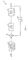
- FIG 1 shows a block diagram representation of a phase locked loop 150.
- the master oscillator 100 has a voltage input labeled U M .
- the master oscillator 100 produces highly stable oscillation about some defined center frequency of the oscillator.
- the frequency of oscillation can be varied slightly by varying the value of voltage input U M .
- the master oscillator 100 has a sensitivity rating of K M Hertz per volt (Hz/Volt) which indicates the proportionality between the input voltage and the frequency of oscillation of the output voltage of the master oscillator 100.
- a slave VCO 102 produces an oscillatory output signal whose frequency is dependent upon the value of a voltage input V vco of the slave VCO 102.
- the slave VCO 102 generally has a sensitivity rating of K V Hertz per volt (Hz/Volt) which indicates the proportionality between the input voltage and the frequency of oscillation of the output voltage of the slave VCO 102.
- the master oscillator 100 typically oscillates in a highly stable manner, but is relatively limited with respect to the frequencies at which it may oscillate.
- the slave VCO 102 is typically highly flexible with respect to the frequencies at which it may oscillate, but oscillates in a highly unstable manner.
- the phase locked loop 150 is a circuit which attempts to take advantage of the best properties of the master oscillator 100 and the slave VCO 102, while avoiding the limitations of both.
- the output of the phase locked loop 150 which is also the output of the slave VCO 102, is fed to a "divide by N" (1/N) frequency divider 104.
- the "divide by N" frequency divider 104 accepts as input a voltage waveform having a frequency of f 1 and transmits as output a "divided by N" frequency version of the f 1 frequency waveform.
- the output of the 1/N frequency divider 104 is fed into one input of a differential frequency/phase voltage controller 106.
- the output of master oscillator 100 is fed into another input of the differential frequency/phase voltage controller 106.
- Differential frequency/phase voltage controller 106 is shown as a summing junction in negative feedback configuration. This configuration indicates that the differential frequency/phase voltage controller 106 will produce substantially constant output (e.g., zero) if its two inputs are the same, but will produce some change in its output if its two inputs are different. For example, in the situation where the differential frequency/phase voltage controller 106 detects that the voltage waveform emerging from the 1/N frequency divider 104 is "lagging" the voltage waveform emerging from the master oscillator 100, the differential frequency/phase voltage controller 106 would slightly increase its output voltage to cause a corresponding increase of the output frequency of the waveform produced by the slave VCO 102.
- the differential frequency/phase voltage controller 106 detects that the voltage waveform emerging from the 1/N frequency divider 104 is "leading" the voltage waveform emerging from master oscillator 100, in one implementation the differential frequency/phase voltage controller 106 would slightly decrease its output voltage to cause a correspondent decrease of the output frequency of the waveform produced by the slave VCO 102.
- differential frequency/phase voltage controller 106 is actually detecting a frequency differential, if the depicted frequency differential is viewed as being “relative to” the 100 kHz reference frequency produced by the master oscillator 100, from the standpoint of the differential frequency/phase voltage controller 106 it appears “as if" the output voltage of the 1/10 frequency divider 104 is "out of phase” ( e.g ., either “lagging” or “leading” in time) with the 100 kHz reference frequency waveform. Consequently, those having ordinary skill in the art often refer to the differential frequency/phase detector portion ( e.g ., see Figure 3 ) of the differential frequency/phase voltage controller 106 solely as a "phase detector.”
- the one block which has not yet been discussed is a loop filter 108 block.
- the differential frequency/phase voltage controller 106 determines the difference in frequency/phase between its inputs, and outputs a voltage signal corresponding to the difference in more-or-less real time. As also noted, this output signal of the differential frequency/phase voltage controller 106 is ultimately used to drive the slave VCO 102. If the slave VCO 102 is allowed to respond to every real time voltage fluctuation of the differential frequency/phase voltage controller 106, the slave VCO 102 will often "overreact” and produce a relatively unstable output voltage waveform. Better stability is achieved by making the slave VCO 102 "less sensitive" to the more quickly varying changes of the voltage output of the differential frequency/phase voltage controller 106.
- a communications system is characterized by: a master oscillator having an output operably coupled to a first input of a phase detector; a slave oscillator having an output operably coupled to a second input of the phase detector; and a forward-gain-adaptation module having a first input operably coupled to a raw-error terminal of the phase detector.
- a method for controlling a communications system includes: adjusting a feed-forward gain of a phase locked loop in response to a raw-error signal of the phase locked loop; and adjusting a slave oscillator of the phase locked loop in response to the feed-forward gain.
- a communications system in another embodiment, includes: a master oscillator having an output operably coupled to a first input of a phase detector; a slave oscillator having an output operably coupled to a second input of the phase detector; and a forward-gain-adaptation module having a first input operably coupled to a filtered-error terminal of the phase detector.
- a method for controlling a communications system includes: adjusting a feed-forward gain of a phase locked loop in response to a filtered-error signal of a phase locked loop; creating a disturbance-cancelled filtered-error signal; and adjusting a slave oscillator of the phase locked loop in response to the feed-forward gain and the disturbance-cancelled filtered-error signal.
- Figure 1 shows a block diagram representation of a phase locked loop.
- Figure 2 shows a high-level block diagram of a phase locked loop wherein two-point modulation is utilized.
- Figure 3 shows a block diagram of a phase locked loop which is represented in Laplace transformed format.
- Figure 4 shows a schematic diagram of one implementation of the loop filter.
- Figure 5A depicts an alternative system version of the system depicted in Figures 2-4 , where the alternative version is substantially the system of Figure 3 augmented by two extra signals: a first signal, ⁇ , to indicate some uncontrollable and unexpected external influence to the system (e.g ., noise), and an internal canceling signal, D, which is intended to cancel the residual influence of ⁇ which is not counteracted by the loop filter.
- a first signal ⁇
- D internal canceling signal
- Figure 5B shows the system of Figure 5A represented in what those skilled in the art will recognize as somewhat analogous to a Laplace-transformed second order system "standard equation,” or “canonical” form.
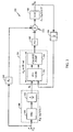
- Figure 6A shows the system of Figure 5B having an additional forward-gain-adaptation module.
- Figure 6B illustrates the system depicted in Figure 6A , shown with additional augmentation components in the forward-gain-adaptation module.
- Figure 7A illustrates a system somewhat similar to the system depicted in Figure 6A , but with different connections and the addition of a disturbance-cancellation module.
- Figure 7B illustrates a system somewhat similar to the system depicted in Figure 7A , but with additional components.
- Figure 8A shows a system which favors mainly digital implementation.
- Figure 8B depicts a system which favors mainly analog implementation.
- Figure 9A shows a system having a phase locked loop, somewhat analogous to the phase locked loop shown and discussed in relation to Figure 3 , but augmented with a linear model of a ⁇ modulator.
- Figure 9B shows a system having a phase locked loop, which is substantially mathematically equivalent to phase locked loop of Figure 9A , but which has been manipulated such that the phase locked loop appearing in Figure 9B has a substantially similar topology to the phase locked loop of Figure 5A .
- Figure 10A shows a system having the ⁇ Fractional- N phase locked loop of Figure 9B , but with an additional forward-gain-adaptation module which implements the above-described raw-error adapted system rule as described in relation to Figure 6B .
- Figure 10B depicts the system of Figure 10A having additional augmentation components in the forward-gain-adaptation module.
- Figure 11A shows a system having the ⁇ Fractional- N phase locked loop of Figure 9B , but with additional modules which help implement the above-described filtered-error adapted system rules as described in relation to Figure 7A .
- Figure 11B illustrates a representation of a system somewhat similar to the system depicted in Figure 11A , but with additional components.
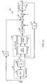
- FIG. 2 shows a high-level block diagram of a phase locked loop 250 employing two-point modulation.
- a voltage input U m of a master oscillator 100 feeds a variable gain amplifier 200, where the variable gain amplifier 200 has a feed-forward gain K u .
- An output of the variable gain amplifier 200 feeds a summation junction 202, which is shown interposed between a loop filter 108 and a slave VCO 102.
- the remaining components of the phase locked loop 250 function in a similar fashion as described in relation to Figure 1 .
- the variable gain amplifier 200 enhances the overall operational bandwidth (i. e., a band of frequencies within which the phase locked loop 250 is viable) of the phase locked loop 250 beyond that associated with the phase locked loop 150 of Figure 1 , if the feed-forward gain K u is set to a correct value.
- measurement devices such as an oscilloscope, or a spectral density meter
- the feed-forward gain K u manually adjusted (e.g ., via use of a screwdriver), to substantially maximize the overall operational bandwidth of the phase locked loop 250.
- technicians generally implement these techniques in an ad-hoc fashion, rather than in conformance with any defined engineering rules.
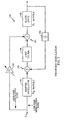
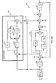
- Figure 3 shows a block diagram of a phase locked loop 350 which is represented in a Laplace transformed format.
- the Laplace transform is used to transform a set of integrodifferential equations from the time domain to a set of algebraic equations in ,the frequency domain.
- the solution for an unknown quantity is therefore reduced to the manipulation of algebraic equations.
- the frequency domain expression for the unknown is obtained, it can be inverse-transformed back to the time domain using known techniques.
- the Laplace transformed format block diagram circuits and devices described herein are representative of their time domain representations, and vice versa.
- a master oscillator 300 in conjunction with a 1/M frequency divider 302 forms the master oscillator 100.
- the 1/M frequency divider 302 adds stability to the master oscillator 100.
- the master oscillator 300 feeds an input of the "divide by M" (1/M) frequency divider 302.
- An output of the 1/M frequency divider 302 is coupled to an input of the differential phase/frequency voltage controller 106.
- the differential phase/frequency voltage controller 106 is composed of a differential phase/frequency detector 304 which feeds a charge pump 306.
- the output of the charge pump 306 is coupled to an input of the loop filter 108 (shown as being represented in the Laplace transformed s-domain).
- An output of the loop filter 108 is coupled to an input of the summing junction 202.
- An output of the variable gain amplifier 200 is coupled to an input of the summing junction 202, while an input of the variable gain amplifier 200 is coupled to the input U M of the master oscillator 300.
- An output of the summing junction 202 is coupled to an input of a slave VCO 102.
- An output of the slave VCO 102 is coupled to an input of a "divide by N" (1/N) frequency divider 104.
- An output of the "divide by N" (1/N) frequency divider 104 is coupled to an input of the differential phase/frequency detector 304.
- Figure 4 shows a schematic diagram of one implementation of the loop filter 108.
- resistance R 2 and capacitance C 2 control the loop dynamics. Consequently, the following discussion herein mainly takes into account only the effects of resistance R 2 and capacitance C 2 . However, the remaining components shown in Figure 4 can be taken into consideration, especially if numerical simulation of the processes and devices shown and described herein is performed.
- Figure 5A depicts an alternative system 550.
- Alternative system 550 is substantially similar to the system of Figure 3 , augmented by two extra signals: a first signal, ⁇ , to indicate some uncontrollable and unexpected external influence to the system (e.g ., noise), and an internal canceling signal, D, which is intended to cancel the residual influence of ⁇ which is not counteracted by the loop filter 108.
- Internal canceling signal, D is explained in more detail in relation to Figures 7A and 7B , below.
- Figure 5B shows the system of Figure 5A represented in what those skilled in the art will recognize as somewhat analogous to a Laplace-transformed second order system "standard equation,” or “canonical” form.
- the standard equation, or canonical, representation of Figure 5B is equivalent to that of Figure 5A , but is easier to manipulate and compare than a system not which is not written in canonical form, because many system manipulation techniques use nomenclature similar to that of Figure 5B .
- the representation of Figure 5B is the result of mathematical substitutions and algebraic manipulations whose details need not be discussed here.
- representing the system as shown in Figure 5B allows certain state equations to be written by inspection, which in one implementation proves advantageous.
- the inventor has determined that it is desirable that the canonical feed-forward gain K ⁇ U be such that the transfer function of the system shown in Figure 5B preferably reduce to that of a near-ideal oscillator.
- the adaptation equations are derived under the condition that the rate of change of energy of the error (either raw or filtered) is always negative. That is, over time, the error tends to zero.
- Figure 6A shows the system of Figure 5B having an additional forward-gain-adaptation module 600 which implements the foregoing rule.
- the raw-error rule states, that in one implementation, the canonical feed-forward gain, K ⁇ U , which will tend to make the system behave as a near-ideal oscillator, can be found by integrating ⁇ 1 times the product of the canonical input, ⁇ M , and the raw-error signal, y 1 .
- ⁇ 1 is a positive constant that helps determine the rapidity of the adaptation.
- the raw-error rule is based on stability arguments, and is intended to make it likely that the entire Phase Locked Loop/Adaptation system is stable for all values of ⁇ 1 .
- the components which substantially implement the raw-error adaptation rule are leading multiplier 606, forward-gain-adaptation module variable gain amplifier 602, having a gain of ⁇ 1 , and forward-gain-adaptation module integrator 604.
- the canonical input ⁇ M is coupled to an input of the leading multiplier 606.
- a raw-error y 1 terminal (carrying raw-error signal y 1) is coupled to an input of the leading multiplier 606.
- the output of leading multiplier 606 is coupled to an input of a forward-gain-adaptation module variable gain amplifier 602 having a gain of ⁇ 1 .
- the output of the forward-gain-adaptation module variable gain amplifier 602 is coupled to the input of the forward-gain-adaptation module integrator 604.
- Connected to an input of a trailing multiplier 616 are both the output of the forward-gain-adaptation module integrator 604 and a canonical version of the input signal, ⁇ M .
- the output of the trailing multiplier 616 is operably coupled with an input of the summing junction 202.
- proportional-contribution variable gain amplifiers are described herein (e.g., proportional-contribution variable gain amplifier 610, described below, and proportional-contribution variable gain amplifier 710, described below), those having ordinary skill in the art will recognize that such proportional-contribution variable gain amplifiers appearing and described herein are to be representative of controllers such as proportional-integral (PI) controllers and proportional-integral-derivative (PID) controllers.
- PI proportional-integral
- PID proportional-integral-derivative
- voltage controlled oscillators are actually non-linear, there exists recognized ranges of operations of voltage controlled oscillators, which, for engineering purposes, can be treated as substantially linear. Consequently, the discussion herein treats voltage controlled oscillators as substantially linear, as is often done in engineering applications. Although the use of "divide by N" circuits are described herein, in other implementations the voltage controlled oscillators are down converted with mixers, rather than with "divide by N" circuits.
- the slave VCO 102 may have a response that is not completely modeled by an ideal oscillator (such as is shown in Figure 6A ), or that there may be other un-modeled dynamics, such as additional components in the loop filter of Figure 6A , and that these differences between practical systems and the modeled systems limit the maximum magnitude of ⁇ 1 over which the phase locked loop of Figure 6A will remain viable.
- the inventor has found it advantageous to augment the raw-error rule with a proportional contribution ( ⁇ 2 ), and a 'leakage' factor ( ⁇ 1 ).
- the proportional control can be conceived of as being used to accelerate the adaptation, while the leakage factor can be conceived of as being one of several methods available to make the adaptive system robust with respect to disturbances and un-modeled dynamics.
- An alternative system implementing the proportional contribution and the leakage factor augmentation of the basic foregoing-described raw-error rule is shown following in Figure 6B .
- Figure 6B illustrates the system depicted in Figure 6A , shown with additional augmentation components in the forward-gain-adaptation module 600.
- forward-gain-adaptation module 600 is driven, at least in part, with what can be characterized as the "raw-error" signal y 1 .
- the signal y 1 is referred to herein as the "raw-error” signal to distinguish it from what is referred to herein as the "filtered-error” signal y 2 .
- the canonical input ⁇ M is coupled to an input of the leading multiplier 606.
- the raw-error y 1 is coupled to an input of the leading multiplier 606.
- the output of leading multiplier 606 is coupled to an input of a forward-gain-adaptation module variable gain amplifier 602 having a gain of ⁇ 1 .
- the output of the forward-gain-adaptation module variable gain amplifier 602 is coupled to the input of a summing junction 608.
- the output of the summing junction 608 is coupled to the input of a forward-gain-adaptation module integrator 604.
- the output of the forward-gain-adaptation module integrator 604 is connected in negative feedback fashion to an input of the summing junction 608, where the negative feedback is provided by leakage-factor variable gain amplifier 612 having a gain of ⁇ 1 .
- the output of the forward-gain-adaptation module integrator 604 is coupled to an input of a summing junction 614. Also connected to an input of the summing junction 614 is an output of the proportional-contribution variable gain amplifier 610 having a gain of ⁇ 2 . The input the proportional-contribution variable gain amplifier 610 is coupled to the output of the leading multiplier 606.
- An output of the summing junction 614 is coupled to the input of the trailing multiplier 616.
- Connected to an input of the trailing multiplier 616 is a canonical version of the input signal, ⁇ M .
- the output of the trailing multiplier 616 is operably coupled with an input of the summing junction 202.
- the adaptation equations are derived under the condition that the rate of change of energy of the error (either raw or filtered) is always negative. That is, over time, the error tends to zero.
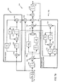
- Figure 7A shows modules 600 and 700 which implement the foregoing rules.
- the filtered-error rule states that, in one implementation, the system of Figure 7A can be made to approach the behavior of an ideal oscillator provided that the canonical feed-forward gain, K ⁇ U , is found by integrating ⁇ 1 times the product of the canonical input, ⁇ M , and the filtered-error, y 2 , and further provided that a disturbance-cancellation factor, D, which is found by integrating ⁇ 3 times the filtered-error, y 2 , be injected into the system.
- ⁇ 1 and ⁇ 3 are positive constants that help determine the rapidity of the adaptation.
- the components which substantially implement the filtered-error adaptation rule are the forward-gain-adaptation module 600 components of the leading multiplier 606, forward-gain-adaptation module variable gain amplifier 602, having a gain of ⁇ 1 , and forward-gain-adaptation module integrator 604, and the disturbance-cancellation module 700 components of a disturbance-cancellation-module variable gain amplifier 702, having a gain of ⁇ 3 , and an disturbance-cancellation-module integrator 704.
- FIG. 7A The system shown in Figure 7A is similar to the system depicted in Figure 6A , but with different connections and the addition of a disturbance-cancellation module 700.
- the forward-gain-adaptation module 600 is driven, at least in part, with what those skilled in the art will appreciate can be the filtered-error signal y 2 . That is, whereas in Figure 6A one input to the leading multiplier 606 was the raw-error signal y 1 , in Figure 7A that same input is now shown as the filtered-error signal y 2 . Otherwise, the connections are as shown and described in relation to Figure 6A , and consequently the discussion of those components common with Figure 6A will not be repeated here.
- the filtered-error signal y 2 is coupled to an input of the disturbance-cancellation-module variable gain amplifier 702 having a gain of ⁇ 3 .
- the output of the disturbance-cancellation-module variable gain amplifier 702 having a gain of ⁇ 3 is coupled to the input of the disturbance-cancellation-module integrator 704.
- the output of the disturbance-cancellation-module integrator 704 is coupled to an input of a summing junction 720.
- An input of a summing junction 720 is coupled with the filtered-error signal y 2 .
- An output of the summing junction 720 is coupled with an input of the summing junction 202.
- the plant (slave VCO) 102 may have a response that is not completely modeled by a pure integrator (such as is shown in Figure 7A ), or that there may be other un-modeled dynamics, such as additional components in the loop filter 108, and that these differences between practical systems and the modeled systems limit the maximum magnitude of ⁇ 3 over which the system shown in Figure 7A is viable.
- the inventor has found it advantageous to augment the filtered-error rule with the proportional contribution factors ⁇ 2 , ⁇ 4 , and the leakage factors ⁇ 1, ⁇ 2.
- An alternative system implementing the proportional contribution and the leakage augmentations of the basic foregoing-described filtered-error rule is shown following in Figure 7B .
- Figure 7B illustrates a system somewhat similar to the system depicted in Figure 7A , but with additional components in modules 600 and 700.
- forward-gain-adaptation module 600 is similar to forward-gain-adaptation module 600 of Figure 6B , but is driven, at least in part, with what those skilled in the art will appreciate can be characterized as the filtered-error signal y 2 . That is, whereas in Figure 6B one input to the leading multiplier 606 was the raw-error signal y 1 , in Figure 7B that same input is now shown as the filtered-error signal y 2 . Otherwise, the connections are as shown and described in relation to Figure 6B , and consequently the discussion of those components common with Figure 6B will not be repeated here.
- the filtered-error signal y 2 is coupled to an input of the disturbance-cancellation-module variable gain amplifier 702 having a gain of ⁇ 3 .
- the output of the disturbance-cancellation-module variable gain amplifier 702 having a gain of ⁇ 3 is coupled to an input of a summing junction 708.
- the output of the summing junction 708 is coupled to an input of a disturbance-cancellation-module integrator 704.
- the output of the disturbance-cancellation-module integrator 704 is coupled in negative feedback fashion to an input of the summing junction 708, where the negative feedback is provided by disturbance-cancellation-module leakage-factor variable gain amplifier 712 having a gain of ⁇ 2 .
- the output of the disturbance-cancellation-module integrator 704 is coupled to the input of the summing junction 714. Coupled to the input of the summing junction 714 is the output of the disturbance-cancellation-module proportional-contribution variable gain amplifier 710 having a gain of ⁇ 4 . An input of the disturbance-cancellation-module proportional-contribution variable gain amplifier 710 is coupled to the "filtered-error" y 2 .
- the output of the summing junction 714 is coupled to an input of the summing junction 720.
- An input of a summing junction 720 is coupled with the filtered-error signal y 2 .
- An output of the summing junction 720 is coupled with an input of the summing junction 202.
- an implementer may opt for a hardware and/or firmware vehicle; alternatively, if flexibility is paramount, the implementer may opt for a solely software implementation; or, yet again alternatively, the implementer may opt for some combination of hardware, software, and/or firmware.
- any vehicle to be utilized is a choice dependent upon the context in which the vehicle will be deployed and the specific concerns (e.g ., speed, flexibility, or predictability) of the implementer, any of which may vary.
- signal bearing media include, but are not limited to, the following: recordable type media such as floppy disks, hard disk drives, CD ROMs, digital tape, and computer memory; and transmission type media such as digital and analog communication links using TDM or IP based communication links ( e.g ., packet links).
- electrical circuitry includes, but is not limited to, electrical circuitry having at least one discrete electrical circuit, electrical circuitry having at least one integrated circuit, electrical circuitry having at least one application specific integrated circuit, electrical circuitry forming a general purpose computing device configured by a computer program (e.g ., a general purpose computer configured by a computer program which at least partially carries out processes and/or devices described herein, or a microprocessor configured by a computer program which at least partially carries out processes and/or devices described herein), electrical circuitry forming a memory device (e.g ., forms of random access memory), and electrical circuitry forming a communications device (e.g ., a modem, communications switch, or optical-electrical
- FIGS. 8A and 8B show examples of systems into which at least a part of the herein described devices and/or processes may be integrated with a reasonable amount of experimentation.
- Figure 8A shows a system particularly suited to digital implementation.
- the partition between the digital and analog portions is marked on Figure 8A .
- the system may optionally include a mixer to down-convert the output.
- the master oscillator, loop filter and adaptation circuitry are digital.
- the output of the VCO enters a ⁇ down-converter to form an error with a digital oscillator.
- the output of the loop filter and adaptation circuits is converted to an analog signal and applied to the input of the VCO.
- Figure 8B depicts a system particularly suited to analog implementation.
- the partition between the digital and analog portions is marked on Figure 8B .
- the system of Figure 8B is an alternative approach to that of Figure 8A , in that the partition of Figure 8B favors analog circuitry. This approach is suitable for adaptation algorithms such as have been described herein.
- a phase locked loop may be modulated by dynamically changing the loop divider ratio, N.
- N can be controlled with a ⁇ -modulator to allow a fractional rather than integer value.
- two-point modulation can be applied to such ⁇ fractional- N loops, as will now be shown.
- Figure 9A shows a system having a phase locked loop 900, somewhat analogous to the phase locked loop 350 ( Figure 3 ), but augmented with a linear model of a ⁇ modulator.
- the ⁇ modulator typically acts to alter the division ratio of the loop
- Figure 9A shows a linearized version of a ⁇ modulator, in which (constant) N represents the nominal division ratio. The small changes in division ratio are represented by the injected phase modulation, ⁇ MOD .
- a linearized version of a ⁇ modulator typically generates a high resolution signal using only a few levels.
- a ⁇ modulator generally achieves the foregoing by dithering the output between levels such that, when filtered, the output has the desired value.
- the ⁇ modulator is typically implemented in digital circuitry. Then, the division ratio N is dithered between several discrete values, such that the required value is generated when filtered by the low-pass filtering action of the phase locked loop.
- linearized ⁇ modulators in part or in whole, are shown, described, and/or referenced herein, such partial or whole linearized ⁇ modulators are meant to be representative of partial or whole linearized analytic versions of ⁇ modulators, as well as substantially all the partial or whole physical component implementations of ⁇ modulators.
- the phase locked loop 900 has two inputs: an upper input R CH , and a lower input R MD .
- the upper input R CH is constant and sets the frequency of the channel. (That is, the frequency about which the modulated spectrum is centered.)
- the lower input R MD varies with time and causes a frequency modulation of VCO 902. This frequency modulation is converted to phase modulation ⁇ MOD and injected into the phase locked loop 900.
- the inventor has discovered that the ⁇ fractional- N phase locked loop 900 can be transformed such that the processes and devices described previously can be applied to the phase locked loop 900.
- This transformation can be understood as follows.
- K U MD K U CH K M MD K M CH ⁇ M N
- phase locked loop 950 and the phase locked loop 550 are topologically substantially identical.
- phase locked loop 950 of Figure 9B arising from the above-described mathematical transformations, is substantially similar to the phase locked loop 550, the inventor has created ⁇ fractional- N phase locked loops which incorporate the foregoing described processes and devices. These ⁇ fractional- N phase locked loops will now be described.
- Figure 10A shows a system having the ⁇ fractional- N phase locked loop 950 of Figure 9B , but with an additional forward-gain-adaptation module 600 which implements the above-described raw-error adapted system rule as described in relation to Figure 6B .
- phase locked loop 950 of Figure 10A functions substantially similarly to the phase locked loop 550 of Figure 6A , and a description of such functioning will not explicitly be set forth here for sake of brevity.
- Figure 10B depicts the system of Figure 10A having additional augmentation components in the forward-gain-adaptation module 600.
- phase locked loop 950 of Figure 10B functions substantially similarly to the phase locked loop 550 of Figure 6B , and hence a description of such functioning will not explicitly be set forth here for sake of brevity.
- Figure 11A shows a system having the ⁇ Fractional- N phase locked loop 950 of Figure 9B , but with additional modules 600 and 700 which help implement the above-described filtered-error adapted system rules as described in relation to Figure 7A .
- phase locked loop 950 of Figure 11A functions substantially similarly to the phase locked loop 550 of Figure 7A , and hence a description of such functioning will not explicitly be set forth here for sake of brevity.
- phase locked loop 950 of Figure 11B functions substantially similarly to the phase locked loop 550 of Figure 7B , and hence a description of such functioning will not explicitly be set forth here for sake of brevity.
- loops and/or systems shown herein may be partitioned between digital and analog domains in many different ways.
- any two components herein combined to achieve a particular functionality can be seen as “associated with” each other such that the desired functionality is achieved, irrespective of architectures or intermedial components.
- any two components so associated can also be viewed as being “operably connected”, or “operably coupled”, to each other to achieve the desired functionality.
- a communications system comprising:
- the forward-gain-adaptation module having a first input operably coupled to a raw-error terminal of the phase detector may comprise:
- the forward-gain-adaptation module variable gain amplifier operably coupled with the raw-error terminal of the phase detector may comprise:
- the forward-gain-adaptation module integrator operably coupled with said forward-gain-adaptation module variable gain amplifier and said slave oscillator may comprise:
- the forward-gain-adaptation module integrator having an input operably coupled with an output of said forward-gain-adaptation module variable gain amplifier may comprise:
- the trailing multiplier having a first input operably coupled to an output of said forward-gain-adaptation module integrator, a second input operably coupled to the input of said master oscillator, and an output operably coupled to an input of said slave oscillator may comprise:
- the communications system may comprise a hand-held phone or a communications base station.
- the slave oscillator having an output operably coupled to a second input of the phase detector may further comprise a ⁇ -modulator operably coupled between the output of the slave oscillator and the second input of the phase detector.
- the ⁇ -modulator may comprise at least one of a voltage controlled oscillator and a summing junction.
- a method for controlling a communications system comprising:
- Adjusting a feed-forward gain of a phase locked loop in response to a raw-error signal of the phase locked loop may comprise:
- Controlling the time rate of change of the feed-forward gain proportional to a time history of the raw-error signal may comprise:
- Integrating the product may comprise:
- Integrating the product may comprise:
- Adjusting the feed-forward gain in response to said integrating the product may comprise:
- Adjusting a slave oscillator of the phase locked loop in response to the feed-forward gain may comprise:
- a communications system comprising:
- the forward-gain-adaptation module having a first input operably coupled to a filtered-error terminal of the phase detector may comprise:
- the forward-gain-adaptation module variable gain amplifier operably coupled with the filtered-error terminal of the phase detector may comprise:
- the forward-gain-adaptation module integrator operably coupled with said forward-gain-adaptation module variable gain amplifier and said slave oscillator may comprise:
- the forward-gain-adaptation module integrator having an input operably coupled with an output of said forward-gain-adaptation module variable gain amplifier may comprise:
- the trailing multiplier having a first input operably coupled to an output of said forward-gain-adaptation module integrator, a second input operably coupled to the input of said master oscillator, and an output operably coupled to an input of said slave oscillator may comprise:
- the communications system may further comprise:
- the disturbance-cancellation module having a first input operably coupled to a filtered-error terminal of the phase detector and a first output operably coupled to said slave oscillator may comprise:
- the slave oscillator operably coupled with an output of said first summing junction may comprise:
- the disturbance-cancellation module having a first input operably coupled to a filtered-error terminal of the phase detector and a first output operably coupled to said slave oscillator may comprise:
- the disturbance-cancellation-module integrator operably coupled with said disturbance-cancellation-module variable gain amplifier and said slave oscillator may comprise:
- the disturbance-cancellation-module integrator having an input operably coupled with an output of said disturbance-cancellation-module variable gain amplifier may comprise:
- the disturbance-cancellation-module integrator operably coupled with said disturbance-cancellation-module variable gain amplifier and said slave oscillator may comprise:
- the communications system may comprise a hand-held phone or a communications base station.
- the slave oscillator having an output operably coupled to a second input of the phase detector may further comprise a ⁇ -modulator operably coupled between the output of the slave oscillator and the second input of the phase detector.
- the ⁇ -modulator may comprise at least one of a voltage controlled oscillator and a summing junction.
- a method for controlling a communications system comprising:
- Adjusting a feed-forward gain of a phase locked loop in response to a filtered-error signal of a phase locked loop may comprise:
- Controlling the time rate of change of the feed-forward gain proportional to a time history of the filtered-error signal may comprise:
- Integrating the product may comprise:
- Adjusting the feed-forward gain in response to said integrating the product may comprise:
- Creating a disturbance-cancelled filtered-error signal may comprise:
- Integrating the filtered-error signal may comprise:
- Integrating the filtered-error signal may comprise:
- Creating a disturbance-cancelled filtered-error signal may comprise:
- Adjusting a slave oscillator of the phase locked loop in response to the feed-forward gain and the disturbance-cancelled filtered-error signal may comprise:
Landscapes
- Stabilization Of Oscillater, Synchronisation, Frequency Synthesizers (AREA)
- Electrical Discharge Machining, Electrochemical Machining, And Combined Machining (AREA)
- Nitrogen Condensed Heterocyclic Rings (AREA)
- Devices For Executing Special Programs (AREA)
Applications Claiming Priority (3)
| Application Number | Priority Date | Filing Date | Title |
|---|---|---|---|
| US40643502P | 2002-08-28 | 2002-08-28 | |
| US10/442,340 US6909331B2 (en) | 2002-08-28 | 2003-05-20 | Phase locked loop having a forward gain adaptation module |
| EP03749195A EP1532729B1 (de) | 2002-08-28 | 2003-08-28 | Phasenregelkreis und verfahren dazu |
Related Parent Applications (1)
| Application Number | Title | Priority Date | Filing Date |
|---|---|---|---|
| EP03749195.8 Division | 2003-08-28 |
Publications (2)
| Publication Number | Publication Date |
|---|---|
| EP2244375A2 true EP2244375A2 (de) | 2010-10-27 |
| EP2244375A3 EP2244375A3 (de) | 2010-11-03 |
Family
ID=31981399
Family Applications (2)
| Application Number | Title | Priority Date | Filing Date |
|---|---|---|---|
| EP10155392A Withdrawn EP2244375A3 (de) | 2002-08-28 | 2003-08-28 | Phasenregelkreisverfahren und -vorrichtung |
| EP03749195A Expired - Lifetime EP1532729B1 (de) | 2002-08-28 | 2003-08-28 | Phasenregelkreis und verfahren dazu |
Family Applications After (1)
| Application Number | Title | Priority Date | Filing Date |
|---|---|---|---|
| EP03749195A Expired - Lifetime EP1532729B1 (de) | 2002-08-28 | 2003-08-28 | Phasenregelkreis und verfahren dazu |
Country Status (9)
| Country | Link |
|---|---|
| US (1) | US6909331B2 (de) |
| EP (2) | EP2244375A3 (de) |
| JP (5) | JP2005537722A (de) |
| AT (1) | ATE460767T1 (de) |
| AU (1) | AU2003268243A1 (de) |
| CA (1) | CA2496526C (de) |
| DE (1) | DE60331657D1 (de) |
| RU (2) | RU2363096C2 (de) |
| WO (1) | WO2004021559A1 (de) |
Cited By (2)
| Publication number | Priority date | Publication date | Assignee | Title |
|---|---|---|---|---|
| RU2502196C1 (ru) * | 2011-04-21 | 2013-12-20 | Хуавэй Текнолоджиз Ко., Лтд. | Устройство компенсации фазовой ошибки и способ компенсации фазовой ошибки |
| RU2580068C1 (ru) * | 2015-02-24 | 2016-04-10 | Акционерное общество "Научно-производственное предприятие "Исток" имени А.И. Шокина" (АО "НПП "Исток" им. Шокина") | Свч синтезатор частот |
Families Citing this family (24)
| Publication number | Priority date | Publication date | Assignee | Title |
|---|---|---|---|---|
| KR100519482B1 (ko) * | 2002-11-30 | 2005-10-07 | 인티그런트 테크놀로지즈(주) | 전압 제어 발진기의 주파수 이득 변화가 보상된 위상 고정루프 주파수 합성기 |
| KR100547831B1 (ko) * | 2003-06-18 | 2006-01-31 | 삼성전자주식회사 | 가변 데이터 전송률에 대응이 가능한 클럭 및 데이터 복원장치 |
| US7015738B1 (en) * | 2003-06-18 | 2006-03-21 | Weixun Cao | Direct modulation of a voltage-controlled oscillator (VCO) with adaptive gain control |
| TWI242929B (en) * | 2004-12-01 | 2005-11-01 | Ind Tech Res Inst | Clock and data recovery apparatus and method thereof |
| US7643602B2 (en) * | 2005-09-30 | 2010-01-05 | Freescale Semiconductor, Inc. | Method and system for estimating frequency offsets |
| FR2900290B1 (fr) * | 2006-04-19 | 2008-11-21 | Atmel Corp | Procede et systeme pour fournir une pompe de charge pour les applications basse tension |
| US7728690B2 (en) * | 2007-10-19 | 2010-06-01 | Qualcomm, Incorporated | Method and apparatus for compensating for tuning nonlinearity of an oscillator |
| EP2220761B1 (de) * | 2007-11-02 | 2011-03-23 | ST-Ericsson SA | Pll-kalibration |
| US8045669B2 (en) * | 2007-11-29 | 2011-10-25 | Qualcomm Incorporated | Digital phase-locked loop operating based on fractional input and output phases |
| US7868672B2 (en) * | 2008-12-09 | 2011-01-11 | Qualcomm Incorporated | Digital phase-locked loop with two-point modulation and adaptive delay matching |
| WO2010081188A1 (en) * | 2009-01-13 | 2010-07-22 | Locata Corporation Pty Ltd | Method and apparatus for extending the range for tracking errors in phase lock loops |
| US8098103B2 (en) * | 2009-06-12 | 2012-01-17 | Qualcomm Incorporated | PLL disturbance cancellation |
| EP2432128A1 (de) * | 2010-09-17 | 2012-03-21 | Nokia Siemens Networks Oy | Verfahren und System zur Wiederherstellung der Uhr mithilfe der adaptiven Regelkreisverstärkungssteuerung |
| US8634512B2 (en) * | 2011-02-08 | 2014-01-21 | Qualcomm Incorporated | Two point modulation digital phase locked loop |
| US20140106681A1 (en) * | 2012-10-12 | 2014-04-17 | Qualcomm Incorporated | Ku ADAPTATION FOR PHASE-LOCKED LOOP WITH TWO-POINT MODULATION |
| US8901974B2 (en) * | 2013-01-30 | 2014-12-02 | Texas Instruments Deutschland Gmbh | Phase locked loop and method for operating the same |
| CN104378110A (zh) * | 2013-08-15 | 2015-02-25 | 同方威视技术股份有限公司 | 一种扫频信号产生电路 |
| JP2015104053A (ja) * | 2013-11-27 | 2015-06-04 | 株式会社日立国際電気 | 無線機及び基地局 |
| RU2567002C1 (ru) * | 2014-10-10 | 2015-10-27 | Федеральное государственное бюджетное образовательное учреждение высшего профессионального образования Московский авиационный институт (национальный исследовательский университет) (МАИ) | Квазикогерентный модулятор сигналов бинарной фазовой манипуляции |
| RU2582331C1 (ru) * | 2014-10-10 | 2016-04-27 | Федеральное государственное бюджетное образовательное учреждение высшего профессионального образования Московский авиационный институт (национальный исследовательский университет) (МАИ) | Квазикогерентный демодулятор сигналов квадратурной фазовой манипуляции |
| RU2581646C1 (ru) * | 2014-10-10 | 2016-04-20 | Федеральное государственное бюджетное образовательное учреждение высшего профессионального образования Московский авиационный институт (национальный исследовательский университет) (МАИ) | Квазикогерентный модулятор сигналов квадратурной фазовой манипуляции |
| RU2566813C1 (ru) * | 2014-10-10 | 2015-10-27 | Федеральное государственное бюджетное образовательное учреждение высшего профессионального образования Московский авиационный институт (национальный исследовательский университет) (МАИ) | Квазикогерентный демодулятор сигналов бинарной фазовой манипуляции |
| RU184877U1 (ru) * | 2018-07-04 | 2018-11-13 | Акционерное общество "Концерн "Созвездие" | Быстродействующий синтезатор частот с высокой чистотой спектра |
| TWI719811B (zh) * | 2020-01-21 | 2021-02-21 | 瑞昱半導體股份有限公司 | 負回授系統架構及其迴圈濾波器 |
Citations (1)
| Publication number | Priority date | Publication date | Assignee | Title |
|---|---|---|---|---|
| WO1999043080A1 (en) | 1998-02-23 | 1999-08-26 | Tropian, Inc. | Direct digital synthesis of precise, stable angle modulated rf signal |
Family Cites Families (29)
| Publication number | Priority date | Publication date | Assignee | Title |
|---|---|---|---|---|
| DE2914814A1 (de) * | 1979-04-11 | 1980-10-30 | Siemens Ag | Frequenzmodulator |
| JPS61156310U (de) * | 1985-03-20 | 1986-09-27 | ||
| JPS6316703A (ja) * | 1986-07-09 | 1988-01-23 | Fujitsu Ltd | 位相同期形多重周波数変調装置 |
| JPS6372204A (ja) * | 1986-09-12 | 1988-04-01 | Matsushita Electric Ind Co Ltd | 電圧制御発振器の変調感度補正回路 |
| JPS6424632A (en) * | 1987-07-21 | 1989-01-26 | Fujitsu Ltd | Phase locked loop circuit |
| JPH01106507A (ja) * | 1987-10-19 | 1989-04-24 | Kenwood Corp | 周波数変調回路 |
| JPH0236215U (de) * | 1988-09-02 | 1990-03-08 | ||
| US4866404A (en) * | 1988-09-15 | 1989-09-12 | General Electric Company | Phase locked frequency synthesizer with single input wideband modulation system |
| US5027087A (en) * | 1990-02-02 | 1991-06-25 | Motorola, Inc. | Fast-switching frequency synthesizer |
| US5207491A (en) | 1991-01-31 | 1993-05-04 | Motorola Inc. | Fast-switching frequency synthesizer |
| JPH05167441A (ja) * | 1991-12-17 | 1993-07-02 | Casio Comput Co Ltd | Pll発振回路 |
| JPH05327491A (ja) * | 1992-05-20 | 1993-12-10 | Fujitsu Ltd | 周波数シンセサイザ |
| JPH06216949A (ja) * | 1993-01-21 | 1994-08-05 | Matsushita Electric Ind Co Ltd | 送信装置 |
| JPH07176957A (ja) * | 1993-12-21 | 1995-07-14 | Nec Corp | 変調回路 |
| US5483203A (en) | 1994-11-01 | 1996-01-09 | Motorola, Inc. | Frequency synthesizer having modulation deviation correction via presteering stimulus |
| US5515013A (en) * | 1995-04-18 | 1996-05-07 | Sierra Wireless | Fixed compromise equalization for a dual port FM modulator |
| JPH0974315A (ja) * | 1995-09-04 | 1997-03-18 | Toyo Commun Equip Co Ltd | 変調回路 |
| JPH09130434A (ja) * | 1995-11-01 | 1997-05-16 | Tec Corp | 周波数シンセサイザの変調回路 |
| US6008703A (en) * | 1997-01-31 | 1999-12-28 | Massachusetts Institute Of Technology | Digital compensation for wideband modulation of a phase locked loop frequency synthesizer |
| US5983077A (en) * | 1997-07-31 | 1999-11-09 | Ericsson Inc. | Systems and methods for automatic deviation setting and control in radio transmitters |
| US5986512A (en) * | 1997-12-12 | 1999-11-16 | Telefonaktiebolaget L M Ericsson (Publ) | Σ-Δ modulator-controlled phase-locked-loop circuit |
| EP0961412B1 (de) | 1998-05-29 | 2004-10-06 | Motorola Semiconducteurs S.A. | Frequenzsynthetisierer |
| JP3571920B2 (ja) * | 1998-06-19 | 2004-09-29 | 株式会社東芝 | Fm変調回路 |
| US6625197B1 (en) * | 1998-10-27 | 2003-09-23 | Qualcomm Incorporated | Method and apparatus for multipath demodulation in a code division multiple access communication system |
| CA2281522C (en) * | 1999-09-10 | 2004-12-07 | Philsar Electronics Inc. | Delta-sigma based two-point angle modulation scheme |
| JP2002151960A (ja) * | 2000-11-10 | 2002-05-24 | Kenwood Corp | Pll回路 |
| US6552618B2 (en) * | 2000-12-13 | 2003-04-22 | Agere Systems Inc. | VCO gain self-calibration for low voltage phase lock-loop applications |
| US7522011B2 (en) * | 2005-08-15 | 2009-04-21 | Nokia Corporation | High pass modulation of a phase locked loop |
| US7760042B2 (en) * | 2008-06-26 | 2010-07-20 | Infineon Technologies Ag | Phase locked loop based frequency modulator with accurate oscillator gain adjustment |
-
2003
- 2003-05-20 US US10/442,340 patent/US6909331B2/en not_active Expired - Lifetime
- 2003-08-28 EP EP10155392A patent/EP2244375A3/de not_active Withdrawn
- 2003-08-28 WO PCT/US2003/027022 patent/WO2004021559A1/en not_active Ceased
- 2003-08-28 EP EP03749195A patent/EP1532729B1/de not_active Expired - Lifetime
- 2003-08-28 JP JP2004531875A patent/JP2005537722A/ja not_active Withdrawn
- 2003-08-28 DE DE60331657T patent/DE60331657D1/de not_active Expired - Lifetime
- 2003-08-28 AU AU2003268243A patent/AU2003268243A1/en not_active Abandoned
- 2003-08-28 CA CA2496526A patent/CA2496526C/en not_active Expired - Fee Related
- 2003-08-28 AT AT03749195T patent/ATE460767T1/de not_active IP Right Cessation
- 2003-08-28 RU RU2005108614/09A patent/RU2363096C2/ru not_active IP Right Cessation
-
2009
- 2009-05-26 RU RU2009120024/09A patent/RU2009120024A/ru not_active Application Discontinuation
-
2011
- 2011-09-20 JP JP2011204881A patent/JP5653871B2/ja not_active Expired - Lifetime
-
2013
- 2013-10-02 JP JP2013207754A patent/JP5852074B2/ja not_active Expired - Lifetime
-
2014
- 2014-09-11 JP JP2014184876A patent/JP5893696B2/ja not_active Expired - Lifetime
-
2016
- 2016-01-04 JP JP2016000226A patent/JP6254198B2/ja not_active Expired - Lifetime
Patent Citations (1)
| Publication number | Priority date | Publication date | Assignee | Title |
|---|---|---|---|---|
| WO1999043080A1 (en) | 1998-02-23 | 1999-08-26 | Tropian, Inc. | Direct digital synthesis of precise, stable angle modulated rf signal |
Cited By (2)
| Publication number | Priority date | Publication date | Assignee | Title |
|---|---|---|---|---|
| RU2502196C1 (ru) * | 2011-04-21 | 2013-12-20 | Хуавэй Текнолоджиз Ко., Лтд. | Устройство компенсации фазовой ошибки и способ компенсации фазовой ошибки |
| RU2580068C1 (ru) * | 2015-02-24 | 2016-04-10 | Акционерное общество "Научно-производственное предприятие "Исток" имени А.И. Шокина" (АО "НПП "Исток" им. Шокина") | Свч синтезатор частот |
Also Published As
| Publication number | Publication date |
|---|---|
| JP2014053912A (ja) | 2014-03-20 |
| JP2015039179A (ja) | 2015-02-26 |
| CA2496526C (en) | 2013-08-06 |
| JP2012050099A (ja) | 2012-03-08 |
| US6909331B2 (en) | 2005-06-21 |
| JP5893696B2 (ja) | 2016-03-23 |
| ATE460767T1 (de) | 2010-03-15 |
| WO2004021559A1 (en) | 2004-03-11 |
| HK1077935A1 (en) | 2006-02-24 |
| JP2016105606A (ja) | 2016-06-09 |
| CA2496526A1 (en) | 2004-03-11 |
| JP6254198B2 (ja) | 2017-12-27 |
| DE60331657D1 (de) | 2010-04-22 |
| JP5852074B2 (ja) | 2016-02-03 |
| JP5653871B2 (ja) | 2015-01-14 |
| US20040041636A1 (en) | 2004-03-04 |
| EP1532729A2 (de) | 2005-05-25 |
| RU2363096C2 (ru) | 2009-07-27 |
| EP2244375A3 (de) | 2010-11-03 |
| AU2003268243A1 (en) | 2004-03-19 |
| EP1532729B1 (de) | 2010-03-10 |
| RU2009120024A (ru) | 2010-12-10 |
| JP2005537722A (ja) | 2005-12-08 |
| RU2005108614A (ru) | 2005-10-10 |
| WO2004021559A9 (en) | 2004-04-29 |
Similar Documents
| Publication | Publication Date | Title |
|---|---|---|
| US6909331B2 (en) | Phase locked loop having a forward gain adaptation module | |
| JP4246380B2 (ja) | 位相ロックループ変調器制御用のポストフィルタδς | |
| DE602004005689T2 (de) | Verfahren und system zur jitter-kompensation | |
| US6172579B1 (en) | Three point modulated phase locked loop frequency synthesis system and method | |
| EP1612931B1 (de) | Schaltung zur Ansteuerung eines spannungsgesteurten Oszillators für Frequenzmodulation | |
| US7522011B2 (en) | High pass modulation of a phase locked loop | |
| EP1345375A3 (de) | Verfahren und Einrichtung zur Frequenzmodulation | |
| JP4887106B2 (ja) | スペクトラム拡散周波数変調された発振器回路、周波数変調された発振器回路および電磁干渉を低減する方法 | |
| US7995697B2 (en) | Polar modulation / one-point frequency modulation with flexible reference frequency | |
| US6806780B2 (en) | Efficient modulation compensation of sigma delta fractional phase locked loop | |
| HK1077935B (en) | Phase locked loop method and apparatus | |
| CN1717861B (zh) | 使用频率偏移补偿的调制器和方法 | |
| US7020286B2 (en) | Modulation of dynamical systems for communication | |
| US20070058750A1 (en) | Baseband compensation of an offset phase locked loop | |
| EP1612946A1 (de) | Vorrichtung mit einem Sigma-Delta-Modulator und Verfahren zur Erzeugung eines quantisierten Signals in einem Sigma-Delta Modulator | |
| JP4815572B2 (ja) | 補償された高速pll回路 | |
| WO2007055291A1 (ja) | 位相変調装置および無線通信装置 | |
| US20080159438A1 (en) | Methods and apparatus for multi-mode frequency shift keying | |
| JPH05114921A (ja) | 変調特性補正回路 | |
| JPH05122258A (ja) | 4値周波数偏移変調器 |
Legal Events
| Date | Code | Title | Description |
|---|---|---|---|
| PUAI | Public reference made under article 153(3) epc to a published international application that has entered the european phase |
Free format text: ORIGINAL CODE: 0009012 |
|
| PUAL | Search report despatched |
Free format text: ORIGINAL CODE: 0009013 |
|
| 17P | Request for examination filed |
Effective date: 20100303 |
|
| AC | Divisional application: reference to earlier application |
Ref document number: 1532729 Country of ref document: EP Kind code of ref document: P |
|
| AK | Designated contracting states |
Kind code of ref document: A2 Designated state(s): AT BE BG CH CY CZ DE DK EE ES FI FR GB GR HU IE IT LI LU MC NL PT RO SE SI SK TR |
|
| AK | Designated contracting states |
Kind code of ref document: A3 Designated state(s): AT BE BG CH CY CZ DE DK EE ES FI FR GB GR HU IE IT LI LU MC NL PT RO SE SI SK TR |
|
| GRAP | Despatch of communication of intention to grant a patent |
Free format text: ORIGINAL CODE: EPIDOSNIGR1 |
|
| STAA | Information on the status of an ep patent application or granted ep patent |
Free format text: STATUS: THE APPLICATION IS DEEMED TO BE WITHDRAWN |
|
| 18D | Application deemed to be withdrawn |
Effective date: 20130522 |