EP2226833B1 - Herstellungsverfahren eines Dünnschichttransistors - Google Patents
Herstellungsverfahren eines Dünnschichttransistors Download PDFInfo
- Publication number
- EP2226833B1 EP2226833B1 EP10154686.9A EP10154686A EP2226833B1 EP 2226833 B1 EP2226833 B1 EP 2226833B1 EP 10154686 A EP10154686 A EP 10154686A EP 2226833 B1 EP2226833 B1 EP 2226833B1
- Authority
- EP
- European Patent Office
- Prior art keywords
- layer
- forming
- metal catalyst
- silicon layer
- amorphous silicon
- Prior art date
- Legal status (The legal status is an assumption and is not a legal conclusion. Google has not performed a legal analysis and makes no representation as to the accuracy of the status listed.)
- Not-in-force
Links
- 238000004519 manufacturing process Methods 0.000 title claims description 11
- 239000010409 thin film Substances 0.000 title description 4
- 239000010410 layer Substances 0.000 claims description 287
- 229910052751 metal Inorganic materials 0.000 claims description 87
- 239000002184 metal Substances 0.000 claims description 87
- 239000003054 catalyst Substances 0.000 claims description 71
- 229910021420 polycrystalline silicon Inorganic materials 0.000 claims description 60
- 238000000034 method Methods 0.000 claims description 48
- 229910021417 amorphous silicon Inorganic materials 0.000 claims description 47
- 238000009792 diffusion process Methods 0.000 claims description 43
- 239000004065 semiconductor Substances 0.000 claims description 35
- 239000000758 substrate Substances 0.000 claims description 26
- VYPSYNLAJGMNEJ-UHFFFAOYSA-N Silicium dioxide Chemical compound O=[Si]=O VYPSYNLAJGMNEJ-UHFFFAOYSA-N 0.000 claims description 18
- PXHVJJICTQNCMI-UHFFFAOYSA-N Nickel Chemical compound [Ni] PXHVJJICTQNCMI-UHFFFAOYSA-N 0.000 claims description 17
- 238000000137 annealing Methods 0.000 claims description 13
- 239000010949 copper Substances 0.000 claims description 12
- 238000007373 indentation Methods 0.000 claims description 10
- 229910052581 Si3N4 Inorganic materials 0.000 claims description 9
- 239000000377 silicon dioxide Substances 0.000 claims description 9
- 235000012239 silicon dioxide Nutrition 0.000 claims description 9
- HQVNEWCFYHHQES-UHFFFAOYSA-N silicon nitride Chemical class N12[Si]34N5[Si]62N3[Si]51N64 HQVNEWCFYHHQES-UHFFFAOYSA-N 0.000 claims description 9
- QTBSBXVTEAMEQO-UHFFFAOYSA-N Acetic acid Chemical compound CC(O)=O QTBSBXVTEAMEQO-UHFFFAOYSA-N 0.000 claims description 8
- RYGMFSIKBFXOCR-UHFFFAOYSA-N Copper Chemical compound [Cu] RYGMFSIKBFXOCR-UHFFFAOYSA-N 0.000 claims description 6
- VEXZGXHMUGYJMC-UHFFFAOYSA-N Hydrochloric acid Chemical compound Cl VEXZGXHMUGYJMC-UHFFFAOYSA-N 0.000 claims description 6
- KDLHZDBZIXYQEI-UHFFFAOYSA-N Palladium Chemical compound [Pd] KDLHZDBZIXYQEI-UHFFFAOYSA-N 0.000 claims description 6
- 229910052782 aluminium Inorganic materials 0.000 claims description 6
- 229910052802 copper Inorganic materials 0.000 claims description 6
- 238000005530 etching Methods 0.000 claims description 6
- XAGFODPZIPBFFR-UHFFFAOYSA-N aluminium Chemical compound [Al] XAGFODPZIPBFFR-UHFFFAOYSA-N 0.000 claims description 5
- 239000011229 interlayer Substances 0.000 claims description 5
- 238000000059 patterning Methods 0.000 claims description 5
- 239000010931 gold Substances 0.000 claims description 4
- 229910052759 nickel Inorganic materials 0.000 claims description 4
- 229910052709 silver Inorganic materials 0.000 claims description 3
- 229910021578 Iron(III) chloride Inorganic materials 0.000 claims description 2
- BQCADISMDOOEFD-UHFFFAOYSA-N Silver Chemical compound [Ag] BQCADISMDOOEFD-UHFFFAOYSA-N 0.000 claims description 2
- 229910052771 Terbium Inorganic materials 0.000 claims description 2
- ATJFFYVFTNAWJD-UHFFFAOYSA-N Tin Chemical compound [Sn] ATJFFYVFTNAWJD-UHFFFAOYSA-N 0.000 claims description 2
- LDDQLRUQCUTJBB-UHFFFAOYSA-N ammonium fluoride Chemical compound [NH4+].[F-] LDDQLRUQCUTJBB-UHFFFAOYSA-N 0.000 claims description 2
- 229910052787 antimony Inorganic materials 0.000 claims description 2
- WATWJIUSRGPENY-UHFFFAOYSA-N antimony atom Chemical compound [Sb] WATWJIUSRGPENY-UHFFFAOYSA-N 0.000 claims description 2
- 229910052793 cadmium Inorganic materials 0.000 claims description 2
- BDOSMKKIYDKNTQ-UHFFFAOYSA-N cadmium atom Chemical compound [Cd] BDOSMKKIYDKNTQ-UHFFFAOYSA-N 0.000 claims description 2
- PCHJSUWPFVWCPO-UHFFFAOYSA-N gold Chemical compound [Au] PCHJSUWPFVWCPO-UHFFFAOYSA-N 0.000 claims description 2
- 229910052737 gold Inorganic materials 0.000 claims description 2
- RBTARNINKXHZNM-UHFFFAOYSA-K iron trichloride Chemical compound Cl[Fe](Cl)Cl RBTARNINKXHZNM-UHFFFAOYSA-K 0.000 claims description 2
- 239000000463 material Substances 0.000 claims description 2
- 239000000203 mixture Substances 0.000 claims description 2
- 229910052763 palladium Inorganic materials 0.000 claims description 2
- 239000004332 silver Substances 0.000 claims description 2
- GZCRRIHWUXGPOV-UHFFFAOYSA-N terbium atom Chemical compound [Tb] GZCRRIHWUXGPOV-UHFFFAOYSA-N 0.000 claims description 2
- OFIYHXOOOISSDN-UHFFFAOYSA-N tellanylidenegallium Chemical compound [Te]=[Ga] OFIYHXOOOISSDN-UHFFFAOYSA-N 0.000 claims 2
- 238000005247 gettering Methods 0.000 description 23
- 238000002425 crystallisation Methods 0.000 description 22
- 230000008025 crystallization Effects 0.000 description 20
- 229910045601 alloy Inorganic materials 0.000 description 10
- 239000000956 alloy Substances 0.000 description 10
- UBSJOWMHLJZVDJ-UHFFFAOYSA-N aluminum neodymium Chemical compound [Al].[Nd] UBSJOWMHLJZVDJ-UHFFFAOYSA-N 0.000 description 10
- 239000012044 organic layer Substances 0.000 description 6
- ZOKXTWBITQBERF-UHFFFAOYSA-N Molybdenum Chemical compound [Mo] ZOKXTWBITQBERF-UHFFFAOYSA-N 0.000 description 5
- 239000011651 chromium Substances 0.000 description 5
- 229910052750 molybdenum Inorganic materials 0.000 description 5
- 239000011733 molybdenum Substances 0.000 description 5
- 229910000838 Al alloy Inorganic materials 0.000 description 4
- NRTOMJZYCJJWKI-UHFFFAOYSA-N Titanium nitride Chemical compound [Ti]#N NRTOMJZYCJJWKI-UHFFFAOYSA-N 0.000 description 4
- 238000005229 chemical vapour deposition Methods 0.000 description 4
- MGRWKWACZDFZJT-UHFFFAOYSA-N molybdenum tungsten Chemical compound [Mo].[W] MGRWKWACZDFZJT-UHFFFAOYSA-N 0.000 description 4
- 238000005240 physical vapour deposition Methods 0.000 description 4
- 229910021332 silicide Inorganic materials 0.000 description 4
- 239000010936 titanium Substances 0.000 description 4
- VYZAMTAEIAYCRO-UHFFFAOYSA-N Chromium Chemical compound [Cr] VYZAMTAEIAYCRO-UHFFFAOYSA-N 0.000 description 3
- 230000000903 blocking effect Effects 0.000 description 3
- 230000007423 decrease Effects 0.000 description 3
- 239000011521 glass Substances 0.000 description 3
- XUIMIQQOPSSXEZ-UHFFFAOYSA-N Silicon Chemical compound [Si] XUIMIQQOPSSXEZ-UHFFFAOYSA-N 0.000 description 2
- RTAQQCXQSZGOHL-UHFFFAOYSA-N Titanium Chemical compound [Ti] RTAQQCXQSZGOHL-UHFFFAOYSA-N 0.000 description 2
- 229910001080 W alloy Inorganic materials 0.000 description 2
- 229910052804 chromium Inorganic materials 0.000 description 2
- 230000000694 effects Effects 0.000 description 2
- 238000007715 excimer laser crystallization Methods 0.000 description 2
- 239000012535 impurity Substances 0.000 description 2
- 238000002347 injection Methods 0.000 description 2
- 239000007924 injection Substances 0.000 description 2
- 238000000206 photolithography Methods 0.000 description 2
- 239000004033 plastic Substances 0.000 description 2
- -1 poly(benzocyclobutene) Polymers 0.000 description 2
- 238000004151 rapid thermal annealing Methods 0.000 description 2
- FVBUAEGBCNSCDD-UHFFFAOYSA-N silicide(4-) Chemical compound [Si-4] FVBUAEGBCNSCDD-UHFFFAOYSA-N 0.000 description 2
- 229910052710 silicon Inorganic materials 0.000 description 2
- 239000010703 silicon Substances 0.000 description 2
- 229910052719 titanium Inorganic materials 0.000 description 2
- WFKWXMTUELFFGS-UHFFFAOYSA-N tungsten Chemical compound [W] WFKWXMTUELFFGS-UHFFFAOYSA-N 0.000 description 2
- 229910052721 tungsten Inorganic materials 0.000 description 2
- 239000010937 tungsten Substances 0.000 description 2
- UFHFLCQGNIYNRP-UHFFFAOYSA-N Hydrogen Chemical compound [H][H] UFHFLCQGNIYNRP-UHFFFAOYSA-N 0.000 description 1
- BPQQTUXANYXVAA-UHFFFAOYSA-N Orthosilicate Chemical compound [O-][Si]([O-])([O-])[O-] BPQQTUXANYXVAA-UHFFFAOYSA-N 0.000 description 1
- 239000004642 Polyimide Substances 0.000 description 1
- 229910052788 barium Inorganic materials 0.000 description 1
- 230000015572 biosynthetic process Effects 0.000 description 1
- 229910052791 calcium Inorganic materials 0.000 description 1
- 238000006356 dehydrogenation reaction Methods 0.000 description 1
- 238000000151 deposition Methods 0.000 description 1
- 230000005525 hole transport Effects 0.000 description 1
- 229910052739 hydrogen Inorganic materials 0.000 description 1
- 239000001257 hydrogen Substances 0.000 description 1
- 239000004973 liquid crystal related substance Substances 0.000 description 1
- 229910052749 magnesium Inorganic materials 0.000 description 1
- 239000011159 matrix material Substances 0.000 description 1
- RUFLMLWJRZAWLJ-UHFFFAOYSA-N nickel silicide Chemical compound [Ni]=[Si]=[Ni] RUFLMLWJRZAWLJ-UHFFFAOYSA-N 0.000 description 1
- 229910021334 nickel silicide Inorganic materials 0.000 description 1
- 229920000058 polyacrylate Polymers 0.000 description 1
- 229920001721 polyimide Polymers 0.000 description 1
- 229920000642 polymer Polymers 0.000 description 1
- 239000002356 single layer Substances 0.000 description 1
- 239000007790 solid phase Substances 0.000 description 1
- 239000010935 stainless steel Substances 0.000 description 1
- 229910001220 stainless steel Inorganic materials 0.000 description 1
Images


Classifications
-
- H01L29/6675—
-
- H01L29/78696—
-
- H—ELECTRICITY
- H01—ELECTRIC ELEMENTS
- H01L—SEMICONDUCTOR DEVICES NOT COVERED BY CLASS H10
- H01L21/00—Processes or apparatus adapted for the manufacture or treatment of semiconductor or solid state devices or of parts thereof
- H01L21/02—Manufacture or treatment of semiconductor devices or of parts thereof
- H01L21/02104—Forming layers
- H01L21/02365—Forming inorganic semiconducting materials on a substrate
- H01L21/02367—Substrates
- H01L21/0237—Materials
- H01L21/02422—Non-crystalline insulating materials, e.g. glass, polymers
-
- H—ELECTRICITY
- H01—ELECTRIC ELEMENTS
- H01L—SEMICONDUCTOR DEVICES NOT COVERED BY CLASS H10
- H01L21/00—Processes or apparatus adapted for the manufacture or treatment of semiconductor or solid state devices or of parts thereof
- H01L21/02—Manufacture or treatment of semiconductor devices or of parts thereof
- H01L21/02104—Forming layers
- H01L21/02365—Forming inorganic semiconducting materials on a substrate
- H01L21/02436—Intermediate layers between substrates and deposited layers
- H01L21/02439—Materials
- H01L21/02488—Insulating materials
-
- H—ELECTRICITY
- H01—ELECTRIC ELEMENTS
- H01L—SEMICONDUCTOR DEVICES NOT COVERED BY CLASS H10
- H01L21/00—Processes or apparatus adapted for the manufacture or treatment of semiconductor or solid state devices or of parts thereof
- H01L21/02—Manufacture or treatment of semiconductor devices or of parts thereof
- H01L21/02104—Forming layers
- H01L21/02365—Forming inorganic semiconducting materials on a substrate
- H01L21/02518—Deposited layers
- H01L21/02521—Materials
- H01L21/02524—Group 14 semiconducting materials
- H01L21/02532—Silicon, silicon germanium, germanium
-
- H—ELECTRICITY
- H01—ELECTRIC ELEMENTS
- H01L—SEMICONDUCTOR DEVICES NOT COVERED BY CLASS H10
- H01L21/00—Processes or apparatus adapted for the manufacture or treatment of semiconductor or solid state devices or of parts thereof
- H01L21/02—Manufacture or treatment of semiconductor devices or of parts thereof
- H01L21/02104—Forming layers
- H01L21/02365—Forming inorganic semiconducting materials on a substrate
- H01L21/02656—Special treatments
- H01L21/02664—Aftertreatments
- H01L21/02667—Crystallisation or recrystallisation of non-monocrystalline semiconductor materials, e.g. regrowth
- H01L21/02672—Crystallisation or recrystallisation of non-monocrystalline semiconductor materials, e.g. regrowth using crystallisation enhancing elements
-
- H01L27/1214—
-
- H01L27/1277—
-
- H01L29/66757—
-
- H01L29/66765—
Definitions
- aspects of the present invention relate to a thin film transistor (TFT), a method of fabricating the same, and an organic light emitting diode (OLED) display device including the same. More particularly, aspects of the present invention relate to a TFT, a method of fabricating the same, and an OLED display device including the same, where the fabrication process can remove most of a metal catalyst remaining in a semiconductor layer formed from a polycrystalline silicon layer crystallized using the metal catalyst by gettering using a metal etchant.
- TFT thin film transistor
- OLED organic light emitting diode
- TFTs Thin film transistors
- AMLCD active matrix liquid crystal display
- OLED organic light emitting diode
- the leakage current tends to increase when the width of a channel region increases and tends to decrease when the length of the channel region increases.
- the length of the channel region is increased in order to reduce the leakage current, the effect is minor.
- the length of the channel region is increased, the size of the entire device is also increased, and the aperture ratio is reduced. Thus, the length of the channel region is limited.
- TFTs of the prior art and method of producing the same are disclosed in US 2005/023531 A1 , US 5,814,540 A , US 2006/033106A1 and US 2008/157083A1 .
- a TFT having a semiconductor layer formed of a polycrystalline silicon layer crystallized using a metal catalyst has problems in that the leakage current as a function of the size of the channel region of the semiconductor layer cannot be estimated, and the size of the channel region of the semiconductor layer, which will be used to control the leakage current, cannot be determined.
- aspects of the present invention provide a method of fabricating a thin film transistor (TFT) as defined in the claims.
- the fabrication process can remove most of a metal catalyst remaining in a semiconductor layer formed of a polycrystalline silicon layer crystallized using the metal catalyst by gettering using a metal etchant, thus improving the characteristics of the TFT.
- a TFT includes: a substrate; a buffer layer disposed on the substrate; a semiconductor layer disposed on the buffer layer; a gate electrode insulated from the semiconductor layer; a gate insulating layer insulating the semiconductor layer from the gate electrode; and source and drain electrodes insulated from the gate electrode and partially connected to the semiconductor layer, wherein the semiconductor layer comprises at least one groove.
- an OLED display device includes: a substrate; a buffer layer disposed on the substrate; a semiconductor layer disposed on the buffer layer; a gate electrode insulated from the semiconductor layer; a gate insulating layer insulating the semiconductor layer from the gate electrode; source and drain electrodes insulated from the gate electrode and partially connected to the semiconductor layer; an insulating layer disposed on the entire surface of the substrate; a first electrode disposed on the insulating layer and electrically connected to one of the source and drain electrodes; an organic layer; and a second electrode, wherein the semiconductor layer comprises at least one groove.
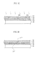
- FIGs. 1A to 1D are cross-sectional views illustrating a crystallization process according to an exemplary embodiment of the present invention for a polycrystalline silicon layer.
- a buffer layer 110 is formed on a substrate 100 that is formed of glass or plastic.
- the buffer layer 110 is an insulating layer and may be formed of a silicon dioxide layer, a silicon nitride layer, or a combination thereof, by chemical vapor deposition (CVD) or physical vapor deposition (PVD).
- the buffer layer 110 serves to prevent diffusion of moisture or impurities generated in the substrate 100 and to adjust the heat transfer rate during crystallization, thereby facilitating crystallization of an amorphous silicon layer.
- the buffer layer 110 is not required in all aspects of the present invention.
- an amorphous silicon layer 120 is formed on the buffer layer 110.
- the amorphous silicon layer 120 may be deposited by CVD or PVD.
- a dehydrogenation process may be performed to reduce the concentration of hydrogen.
- the amorphous silicon layer 120 is crystallized into a polycrystalline silicon layer.
- the amorphous silicon layer is crystallized into a polycrystalline silicon layer by a crystallization method using a metal catalyst, such as a metal induced crystallization (MIC) technique, a metal induced lateral crystallization (MILC) technique, or a super grain silicon (SGS) technique.
- a metal catalyst such as a metal induced crystallization (MIC) technique, a metal induced lateral crystallization (MILC) technique, or a super grain silicon (SGS) technique.
- MIC metal induced crystallization
- MILC metal induced lateral crystallization
- SGS super grain silicon
- the SGS technique is a method of crystallizing an amorphous silicon layer 120 in which the concentration of the metal catalyst diffused into the amorphous silicon layer 120 is lowered in order to control the grain size of the polycrystalline silicon to be within the range of several ⁇ m to several hundreds of ⁇ m.
- a diffusion layer 130 (see FIG. 1 B) is formed on the amorphous silicon layer 120
- a metal catalyst layer 140 (see FIG. 1 B) is formed on the diffusion layer 130 and annealed to diffuse the metal catalyst into the amorphous silicon layer 120.
- FIG. 1 B is a cross-sectional view illustrating a process of forming a diffusion layer 130 and a metal catalyst layer 140 on the amorphous silicon layer 120.
- the diffusion layer 130 is formed on the amorphous silicon layer 120.
- the diffusion layer 130 is formed in a double-layered structure of the silicon nitride layer and the silicon dioxide layer and any one of the layers is patterned to adjust the position where the metal catalyst is diffused.
- the diffusion layer 130 may be formed by any suitable deposition method such as, for example, CVD or PVD.
- the diffusion layer 130 may be formed to a thickness of 0.1 through 200 nm.
- the thickness of the diffusion layer 130 is less than 0.1 nm, it may be difficult to control the amount of metal catalyst that diffuses through the diffusion layer 130.
- the thickness of the diffusion layer 130 is more than 200 nm, the amount of metal catalyst diffused into the amorphous silicon layer 120 may be too small, and thus it is difficult to crystallize the amorphous silicon layer 120 into a polycrystalline silicon layer.
- a metal catalyst is deposited on the diffusion layer 130 to form a metal catalyst layer 140.
- the metal catalyst may be selected from the group consisting of nickel (Ni), palladium (Pd), silver (Ag), gold (Au), aluminum (Al), tin (Sn), antimony (Sb), copper (Cu), terbium (Tb), and cadmium (Cd), and preferably the metal catalyst may be Ni.
- the metal catalyst layer 140 may be formed to have a surface density of 10 11 through 10 15 atoms/cm 2 on the diffusion layer 130.
- the metal catalyst layer 140 When the metal catalyst layer 140 is formed with a surface density of less than 10 11 atoms/cm 2 , the number of seeds, which act as nuclei for crystallization, may be too small, and thus it may be difficult to crystallize the amorphous silicon layer into a polycrystalline silicon layer by the SGS crystallization technique. When the metal catalyst layer 140 is formed with a surface density of more than 10 15 atoms/cm 2 , the amount of metal catalyst diffused into the amorphous silicon layer 120 is too large, and thus the grains produced in the polycrystalline silicon layer are smaller in size. Moreover, the amount of metal catalyst remaining in the polycrystalline silicon layer also increases, and thus the characteristics of a semiconductor layer formed by patterning the polycrystalline silicon layer may be poorer.
- FIG. 1C is a cross-sectional view illustrating a process of diffusing the metal catalyst through the diffusion layer 130 to an interface of the amorphous silicon layer 120 by annealing the substrate 110.
- the substrate 100 on which the buffer layer 110, the amorphous silicon layer 120, the diffusion layer 130, and the metal catalyst layer 140 are formed, is annealed to move some of the metal catalyst of the metal catalyst layer 140 to the surface of the amorphous silicon layer 120.
- the amount of metal catalyst 140b reaching the surface of the amorphous silicon layer 120 is determined by the diffusion blocking ability of the diffusion layer 130, which is closely related to the thickness of the diffusion layer 130. That is, as the thickness of the diffusion layer 130 increases, the diffused amount of the metal catalyst 140b decreases, and thus the produced grains become larger. On the other hand, if the thickness of the diffusion layer 130 decreases, the diffused amount of the metal catalyst 140b increases, and thus the produced grains become smaller.
- the annealing process may be performed at a temperature of about 200 to about 900 °C, preferably at a temperature of about 350 to about 500 °C for several seconds to several hours to diffuse the metal catalyst. Under the annealing conditions described above, it is possible to prevent deformation of the substrate 100 caused by excessive annealing, and to lower production costs and increase yield.
- the annealing process may be one of a furnace process, a rapid thermal annealing (RTA) process, a UV process, and a laser process.
- RTA rapid thermal annealing
- FIG. 1D is a cross-sectional view illustrating a process of crystallizing the amorphous silicon layer 120 into a polycrystalline silicon layer 160 by using the diffused metal catalyst.
- the amorphous silicon layer 120 is crystallized into a polycrystalline silicon layer 160 by the metal catalyst 140b that has diffused to the surface of the amorphous silicon layer 120 through the diffusion layer 130. That is, the diffused metal catalyst 140b is bonded to silicon of the amorphous silicon layer 120 to form metal silicides, which form seeds, i.e., nuclei for crystallization, and thus the amorphous silicon layer 120 is crystallized into the polycrystalline silicon layer 160.
- the annealing process is performed without removing the diffusion layer 130 and the metal catalyst layer 140.
- the polycrystalline silicon layer may be formed by diffusing the metal catalyst 140b onto the amorphous silicon layer 120 to form metal silicides, which are nuclei for crystallization, removing the diffusion layer 130 and the metal catalyst layer 140, and then annealing the bared amorphous silicon layer 120.
- FIGs. 2A and 2B are cross-sectional views illustrating gettering on a polycrystalline silicon layer.
- a buffer layer 210 and a polycrystalline silicon layer 220 crystallized using the metal catalyst according to FIGs.1 A through 1D have been formed on a substrate 200.
- the exemplary gettering that follows is performed on the substrate 200, from which the diffusion layer 130 and the metal catalyst layer 140 illustrated in FIG. 1D have been deleted from FIGs. 2A and 2B for purposes of explanation.
- the polycrystalline silicon layer 220 contains residual metal catalyst 140b, and the concentration of the residual metal catalyst 140b after the crystallization is about 1 ⁇ 10 13 to 5 ⁇ 10 14 atoms/cm 2 .
- the polycrystalline silicon layer 220 is etched with an etchant.
- the etchant used is to remove nickel or nickel silicide and includes a mixture of 25% hydrochloric acid (HCl), 10% acetic acid (CH 3 COOH), and ferric chloride at various concentrations. Moreover, buffered oxide etch (BOE) such as HF or NH 4 F may be used. When the etchant is used to etch the polycrystalline silicon layer 220 for about 2 minutes, the residual metal catalysts are dissolved in the etchant, thus allowing the gettering process to proceed.
- HCl hydrochloric acid
- CH 3 COOH acetic acid
- ferric chloride ferric chloride
- BOE buffered oxide etch
- the substrate 200 on which the polycrystalline silicon layer 220 has been formed is etched, the residual metal catalyst 140b present in the polycrystalline silicon layer 220 is removed. Especially, the metal silicide at the grain interface is dissolved in the etchant and removed, and thus grooves or indentations "a" are formed.
- the formed indentations "a” have various sizes according to the initial concentration of the metal catalyst and the temperature and time of the crystallization annealing process.
- the indentations "a” may have sizes in the range of about 200 to about 1,000 nm, and fine holes may be formed.
- FIG. 2C is a photograph of the surface of the polycrystalline silicon layer 220 taken after gettering with the etchant as illustrated in FIG. 2B , from which it can be seen that the indentations "a" are formed after the aggregated metal catalyst and metal silicide are removed.
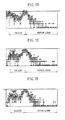
- FIGs. 2D to 2F are graphs of metal catalyst concentrations of the polycrystalline silicon layers to which gettering has been applied, in which the crystallization is performed using nickel as the metal catalyst.
- FIG. 2D shows the concentration of nickel catalyst of the polycrystalline silicon layer measured before gettering
- FIG. 2E shows the concentration of nickel catalyst of the polycrystalline silicon layer measured after gettering for 1 minute
- FIG. 2F shows the concentration of nickel catalyst of the polycrystalline silicon layer measured after gettering for 2 minutes.
- the grooves are formed on the surface of the polycrystalline silicon layer after gettering, the grooves have no significant effect on the characteristics of a semiconductor layer formed from the polycrystalline silicon layer.
- Table 1 shows the characteristics of the semiconductor layer formed from the polycrystalline silicon layer 160 after gettering.
- Table 1 Number of indentations Threshold voltage (Vth)(V) Off-current (loff)(A/ ⁇ m) 4 2.01 2x10 -11 6 1.99 1x10 -11 8 1.98 1x10 -11
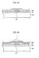
- FIGs. 3A to 3C are cross-sectional views illustrating a process of fabricating a top-gate TFT according to another exemplary embodiment of the present invention using the process of fabricating the polycrystalline silicon layer.
- a buffer layer 310 may be formed on a substrate 300 that is formed of glass, stainless steel, or plastic.
- the buffer layer 310 is an insulating layer and may be formed of a silicon dioxide layer, a silicon nitride layer, or a combination thereof.
- the buffer layer 310 serves to prevent diffusion of moisture or impurities generated in the substrate 300 and to adjust the heat transfer rate during crystallization, thereby facilitating crystallization of an amorphous silicon layer.
- a polycrystalline silicon layer 320a an amorphous silicon layer is formed on the buffer layer 310.
- the amorphous silicon layer is crystallized into a polycrystalline silicon layer 320a using a metal catalyst.
- the polycrystalline silicon layer 320a is subjected to the above-described gettering of FIGs. 2A and 2B using a metal etchant to remove residual metal catalysts, thereby forming a polycrystalline silicon layer 320a having indentations "a" formed with the metal catalyst.
- a semiconductor layer 320 is formed on the buffer layer 310 by patterning the polycrystalline silicon layer 320a. Then, a gate insulating layer 330 is formed on the entire surface of the substrate 300 including the semiconductor layer 320.
- the gate insulating layer 330 may be a silicon dioxide layer, a silicon nitride layer, or a combination thereof.
- a metal layer for a gate electrode (not shown) is formed on the gate insulating layer 330 using a single layer of aluminum (Al) or an Al alloy such as aluminum-neodymium (Al-Nd), or a multi-layer having an Al alloy stacked on a chrome (Cr) or molybdenum (Mo) alloy, and a gate electrode 340 is formed to correspond to a channel region of the semiconductor layer 320 by etching the metal layer for a gate electrode using a photolithography process.
- Al aluminum
- Al-Nd aluminum-neodymium
- Mo molybdenum
- an interlayer insulating layer 350 is formed on the entire surface of the substrate 300 including the gate electrode 340.
- the interlayer insulating layer 350 may be formed of a silicon dioxide layer, a silicon nitride layer, or a combination thereof.
- the interlayer insulating layer 350 and the gate insulating layer 330 are etched to form contact holes exposing source and drain regions of the semiconductor layer 320.
- Source and drain electrodes 360 and 361 connected to the source and drain regions through the contact holes are formed.
- the source and drain electrodes 360 and 361 may be formed of one selected from the group consisting of molybdenum (Mo) or a molybdenum (Mo) alloy, chromium (Cr), tungsten (W) or a (W) tungsten alloy, molybdenum-tungsten (MoW), aluminum (Al) or an aluminum alloy, aluminum-neodymium (Al-Nd), titanium (Ti), titanium-nitride (TiN), or copper (Cu) or a copper (Cu) alloy,.
- TFT including the semiconductor layer 320, the gate electrode 340, and the source and drain electrodes 360 and 361 is completed.
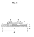
- FIGs. 4A to 4C are cross-sectional views illustrating a process of fabricating a bottom-gate TFT according to another exemplary embodiment of the present invention using the process of fabricating the polycrystalline silicon layer. Except for particular descriptions below, the process will be described with reference to the descriptions in the above exemplary embodiment.
- a buffer layer 410 is formed on a substrate 400.
- a metal layer is formed on the buffer layer 410, and a gate electrode 420 is formed by etching the metal layer for a gate electrode using a photolithography process. Then, a gate insulating layer 430 is formed on the substrate 400 including the gate electrode 420.
- an amorphous silicon layer is formed on the gate insulating layer 430 and then crystallized into a polycrystalline silicon layer 440a using a metal catalyst in the same manner as the exemplary embodiment of FIGS. 1 A through 1 D .
- the polycrystalline silicon layer 440a is subjected to the gettering described in the exemplary embodiment of FIGs. 2A and 2B such that the metal catalyst in the polycrystalline silicon layer 440a is removed by the gettering, and thus grooves or indentations "a" remain.
- a semiconductor layer 440 is formed by patterning the polycrystalline silicon layer 440a. Then, source and drain conductive layers are formed on the semiconductor layer 440 and patterned to form source and drain electrodes 450 and 451.
- the source and drain electrodes 450 and 451 may be formed of one selected from the group consisting of molybdenum (Mo) or a molybdenum (Mo) alloy, chromium (Cr), tungsten (W) or a (W) tungsten alloy, molybdenum-tungsten (MoW), aluminum (Al) or an aluminum alloy, aluminum-neodymium (Al-Nd), titanium (Ti), titanium-nitride (TiN), or copper (Cu) or a copper (Cu) alloy,.
- TFT including the semiconductor layer 440, the gate electrode 420, and the source and drain electrodes 450 and 451 is completed.
- FIG. 5 is a cross-sectional view of an OLED display device including a top-gate TFT produced according to a method of the present invention.
- an insulating layer 365 is formed on the entire surface of the substrate 300 including the TFT produced according to the method exemplified in FIGS. 3A to 3C .
- the insulating layer 365 may be an inorganic layer formed of a material selected from the group consisting of silicon dioxide, silicon nitride, and silicate on glass, or an organic layer formed of a polymer selected from the group consisting of a polyimide, a poly(benzocyclobutene), and a polyacrylate.
- the insulating layer 365 may be formed by stacking the inorganic layer and the organic layer.
- a via hole exposing the source or drain electrode 360 or 361 is formed by etching the insulating layer 365.
- a first electrode 370 connected to one of the source and drain electrodes 360 and 361 through the via hole is formed.
- the first electrode 370 may be an anode or a cathode.
- the anode may be formed of a transparent conductive layer formed of ITO, IZO, or ITZO
- the cathode may be formed of Mg, Ca, Al, Ag, Ba, or an alloy thereof.
- a pixel defining layer 375 having an opening that partially exposes the surface of the first electrode 370 is formed on the first electrode 370, and an organic layer 380 including an emission layer is formed on the exposed first electrode 370.
- the organic layer 380 may further include at least one of a hole injection layer, a hole transport layer, a hole blocking layer, an electron blocking layer, an electron injection layer, and an electron transport layer.
- a second electrode 385 is formed on the organic layer 380.
Landscapes
- Engineering & Computer Science (AREA)
- Microelectronics & Electronic Packaging (AREA)
- Chemical & Material Sciences (AREA)
- Physics & Mathematics (AREA)
- Condensed Matter Physics & Semiconductors (AREA)
- General Physics & Mathematics (AREA)
- Manufacturing & Machinery (AREA)
- Power Engineering (AREA)
- Computer Hardware Design (AREA)
- Crystallography & Structural Chemistry (AREA)
- Chemical Kinetics & Catalysis (AREA)
- Materials Engineering (AREA)
- Thin Film Transistor (AREA)
- Recrystallisation Techniques (AREA)
- Electroluminescent Light Sources (AREA)
- Weting (AREA)
Claims (9)
- Verfahren zur Herstellung einer polykristallinen Siliziumschicht (160, 220), aufweisend die folgende Abfolge von Schritten:Ausbildung einer Pufferschicht (110, 210) auf einem Substrat (100, 200);Ausbildung einer amorphen Siliziumschicht (120) auf der Pufferschicht (110, 210);Ausbildung einer Diffusionsschicht (130) auf der amorphen Siliziumschicht (120), wobei die Diffusionsschicht (130) in einer doppelschichtigen Struktur aus einer Siliziumnitridschicht und einer Siliziumdioxidschicht ausgebildet wird, und wobei irgendeine der besagten Schichten gemustert wird, so dass die Position eingestellt wird, in der ein Metallkatalysator durch die besagte Diffusionsschicht (130) zur besagten amorphen Siliziumschicht (120) diffundieren soll;Ausbildung einer Metallkatalysatorschicht (140) auf der Diffusionsschicht (130);Kristallisation der amorphen Siliziumschicht (120) zu einer polykristallinen Siliziumschicht (160, 220) durch Glühen des Substrats (100, 200);Entfernen der Diffusionsschicht (130) und der Metallkatalysatorschicht (140); undÄtzen der polykristallinen Siliziumschicht (160, 220) mittels eines Ätzmittels.
- Verfahren nach Anspruch 1, wobei die polykristalline Siliziumschicht (160, 220) zumindest eine Vertiefung aufweist, und wobei jede Vertiefung eine Größe von 200 bis 1000 nm aufweist.
- Verfahren zur Herstellung eines Top-Gate-Dünnschichttransistors, aufweisend die folgende Abfolge von Schritten:Ausbildung einer Pufferschicht (310) auf einem Substrat (300);Ausbildung einer amorphen Siliziumschicht auf der Pufferschicht (8);Ausbildung einer Diffusionsschicht auf der amorphen Siliziumschicht, wobei die Diffusionsschicht in einer doppelschichtigen Struktur aus einer Siliziumnitridschicht und einer Siliziumdioxidschicht ausgebildet wird, und wobei irgendeine der besagten Schichten gemustert wird, so dass die Position eingestellt wird, in der ein Metallkatalysator durch die besagte Diffusionsschicht zur besagten amorphen Siliziumschicht diffundieren soll;Ausbildung einer Metallkatalysatorschicht auf der Diffusionsschicht;Kristallisation der amorphen Siliziumschicht zu einer polykristallinen Siliziumschicht (320a) durch Glühen des Substrats (300);Entfernen der Diffusionsschicht und der Metallkatalysatorschicht; undÄtzen der polykristallinen Siliziumschicht (320a) mittels eines Ätzmittels;Ausbildung einer Halbleiterschicht (320) durch Mustern der polykristallinen Siliziumschicht (320a);Ausbildung einer Gate-Isolierschicht (330) auf der Halbleiterschicht (320);Ausbildung einer Gate-Elektrode (340) auf der Gate-Isolierschicht (330);Ausbildung einer Zwischenschicht-Isolierschicht (350) auf der Gesamtfläche des Substrats (300); undAusbildung einer Source- und einer Drain-Elektrode (360, 361) auf der Zwischenschicht-Isolierschicht (350), die teilweise mit der Halbleiterschicht (320) verbunden werden.
- Verfahren zur Herstellung eines Bottom-Gate-Dünnschichttransistors, aufweisend die folgende Abfolge von Schritten:Ausbildung einer Pufferschicht (410) auf einem Substrat (400);Ausbildung einer Gate-Elektrode (420) auf der Pufferschicht (410);Ausbildung einer Gate-Isolierschicht (430) auf der Gesamtfläche des Substrats (400);Ausbildung einer amorphen Siliziumschicht auf der Gate-Isolierschicht (430);Ausbildung einer Diffusionsschicht auf der amorphen Siliziumschicht, wobei die Diffusionsschicht in einer doppelschichtigen Struktur aus einer Siliziumnitridschicht und einer Siliziumdioxidschicht ausgebildet wird, und wobei irgendeine der besagten Schichten gemustert wird, so dass die Position eingestellt wird, in der ein Metallkatalysator durch die besagte Diffusionsschicht zur besagten amorphen Siliziumschicht diffundieren soll;Ausbildung einer Metallkatalysatorschicht auf der Diffusionsschicht;Kristallisation der amorphen Siliziumschicht zu einer polykristallinen Siliziumschicht (440a) durch Glühen des Substrats (400);Entfernen der Diffusionsschicht und der Metallkatalysatorschicht; undÄtzen der polykristallinen Siliziumschicht (440a) mittels eines Ätzmittels;Ausbildung einer Halbleiterschicht (440), die mit der Gate-Elektrode (420) korrespondiert, durch Mustern der polykristallinen Siliziumschicht (440a); undAusbildung einer Source- und einer Drain-Elektrode (450, 451), die einen Abschnitt der Halbleiterschicht (440) freilegen und mit der Halbleiterschicht (440) verbunden sind.
- Verfahren nach Anspruch 3 oder 4, wobei das Ätzmittel zumindest ein Material ist, das aus der Gruppe bestehend aus Salzsäure, Essigsäure, Eisen(III)-chlorid und gepufferter Flusssäure ausgewählt ist.
- Verfahren nach einem der Ansprüche 3 bis 5, wobei die Metallkatalysatorschicht aus einem Metall ausgebildet wird, das aus der Gruppe bestehend aus Nickel (Ni), Palladium (Pd), Silber (Ag), Gold (Au), Aluminium (Al), Zinn (Sn), Antimon (Sb), Kupfer (Cu), Terbium (Tb) und Kadmium (Cd) ausgewählt ist.
- Verfahren nach einem der Ansprüche 3 bis 6, wobei das Glühen bei einer Temperatur von 350 bis 500 °C durchgeführt wird.
- Verfahren nach Anspruch 5, wobei die gepufferte Flusssäure eine Mischung aus HF und NH4F ist.
- Verfahren nach Anspruch 3 oder 4, wobei die Dicke der Diffusionsschicht 0,1 bis 200 nm beträgt.
Applications Claiming Priority (1)
| Application Number | Priority Date | Filing Date | Title |
|---|---|---|---|
| KR1020090018201A KR101015849B1 (ko) | 2009-03-03 | 2009-03-03 | 박막트랜지스터, 그의 제조방법 및 이를 포함하는 유기전계발광표시장치 |
Publications (2)
| Publication Number | Publication Date |
|---|---|
| EP2226833A1 EP2226833A1 (de) | 2010-09-08 |
| EP2226833B1 true EP2226833B1 (de) | 2013-04-10 |
Family
ID=42102476
Family Applications (1)
| Application Number | Title | Priority Date | Filing Date |
|---|---|---|---|
| EP10154686.9A Not-in-force EP2226833B1 (de) | 2009-03-03 | 2010-02-25 | Herstellungsverfahren eines Dünnschichttransistors |
Country Status (5)
| Country | Link |
|---|---|
| US (2) | US20100224883A1 (de) |
| EP (1) | EP2226833B1 (de) |
| JP (1) | JP5355450B2 (de) |
| KR (1) | KR101015849B1 (de) |
| CN (1) | CN101826556B (de) |
Families Citing this family (13)
| Publication number | Priority date | Publication date | Assignee | Title |
|---|---|---|---|---|
| KR101041141B1 (ko) | 2009-03-03 | 2011-06-13 | 삼성모바일디스플레이주식회사 | 유기전계발광표시장치 및 그의 제조방법 |
| KR101049801B1 (ko) | 2009-03-05 | 2011-07-15 | 삼성모바일디스플레이주식회사 | 다결정 실리콘층의 제조방법 및 이에 이용되는 원자층 증착장치 |
| KR101056428B1 (ko) | 2009-03-27 | 2011-08-11 | 삼성모바일디스플레이주식회사 | 박막트랜지스터, 그의 제조방법, 및 이를 포함하는 유기전계발광표시장치 |
| KR101094295B1 (ko) * | 2009-11-13 | 2011-12-19 | 삼성모바일디스플레이주식회사 | 다결정 실리콘층의 제조방법, 박막트랜지스터의 제조방법, 및 유기전계발광표시장치의 제조방법 |
| KR20120131753A (ko) * | 2011-05-26 | 2012-12-05 | 삼성디스플레이 주식회사 | 박막 트랜지스터, 박막 트랜지스터의 제조 방법 및 유기 발광 표시 장치 |
| KR101809661B1 (ko) * | 2011-06-03 | 2017-12-18 | 삼성디스플레이 주식회사 | 박막 트랜지스터, 그 제조 방법 및 이를 포함하는 유기 발광 표시 장치 |
| CN102651401B (zh) * | 2011-12-31 | 2015-03-18 | 京东方科技集团股份有限公司 | 一种薄膜晶体管、阵列基板及其制造方法和显示器件 |
| KR101949861B1 (ko) | 2012-10-10 | 2019-02-20 | 삼성디스플레이 주식회사 | 유기 발광 표시 장치 및 유기 발광 표시 장치의 제조 방법 |
| CN104240633B (zh) * | 2013-06-07 | 2018-01-09 | 上海和辉光电有限公司 | 薄膜晶体管和有源矩阵有机发光二极管组件及其制造方法 |
| KR102301501B1 (ko) * | 2015-01-21 | 2021-09-13 | 삼성디스플레이 주식회사 | 가요성 표시 장치의 제조 방법 |
| CN104570515A (zh) * | 2015-01-26 | 2015-04-29 | 京东方科技集团股份有限公司 | 一种阵列基板及其制备方法、显示面板和显示装置 |
| CN108550583B (zh) | 2018-05-09 | 2021-03-23 | 京东方科技集团股份有限公司 | 一种显示基板、显示装置及显示基板的制作方法 |
| TWI682523B (zh) * | 2019-01-22 | 2020-01-11 | 大陸商深圳市柔宇科技有限公司 | 陣列基板及有機發光二極體顯示裝置 |
Family Cites Families (40)
| Publication number | Priority date | Publication date | Assignee | Title |
|---|---|---|---|---|
| WO1993019022A1 (fr) * | 1992-03-25 | 1993-09-30 | Kanegafuchi Chemical Industry Co., Ltd. | Couche mince de polysilicium et sa fabrication |
| JPH0669515A (ja) * | 1992-08-19 | 1994-03-11 | Fujitsu Ltd | 半導体記憶装置 |
| JP3107941B2 (ja) | 1993-03-05 | 2000-11-13 | 株式会社半導体エネルギー研究所 | 薄膜トランジスタおよびその作製方法 |
| KR100294026B1 (ko) * | 1993-06-24 | 2001-09-17 | 야마자끼 순페이 | 전기광학장치 |
| US7081938B1 (en) * | 1993-12-03 | 2006-07-25 | Semiconductor Energy Laboratory Co., Ltd. | Electro-optical device and method for manufacturing the same |
| TW317643B (de) * | 1996-02-23 | 1997-10-11 | Handotai Energy Kenkyusho Kk | |
| JPH1174536A (ja) * | 1997-01-09 | 1999-03-16 | Sanyo Electric Co Ltd | 半導体装置の製造方法 |
| JP2000031488A (ja) * | 1997-08-26 | 2000-01-28 | Semiconductor Energy Lab Co Ltd | 半導体装置およびその作製方法 |
| KR100317638B1 (ko) | 1999-03-19 | 2001-12-22 | 구본준, 론 위라하디락사 | 폴리실리콘 박막트랜지스터 소자 및 그 제조방법 |
| US6878968B1 (en) * | 1999-05-10 | 2005-04-12 | Semiconductor Energy Laboratory Co., Ltd. | Semiconductor device |
| JP3706527B2 (ja) * | 1999-06-30 | 2005-10-12 | Hoya株式会社 | 電子線描画用マスクブランクス、電子線描画用マスクおよび電子線描画用マスクの製造方法 |
| JP3715848B2 (ja) * | 1999-09-22 | 2005-11-16 | シャープ株式会社 | 半導体装置の製造方法 |
| US6294442B1 (en) * | 1999-12-10 | 2001-09-25 | National Semiconductor Corporation | Method for the formation of a polysilicon layer with a controlled, small silicon grain size during semiconductor device fabrication |
| GB2358081B (en) * | 2000-01-07 | 2004-02-18 | Seiko Epson Corp | A thin-film transistor and a method for maufacturing thereof |
| JP4135347B2 (ja) * | 2001-10-02 | 2008-08-20 | 株式会社日立製作所 | ポリシリコン膜生成方法 |
| US6933527B2 (en) * | 2001-12-28 | 2005-08-23 | Semiconductor Energy Laboratory Co., Ltd. | Semiconductor device and semiconductor device production system |
| TW536716B (en) * | 2002-07-04 | 2003-06-11 | Ind Tech Res Inst | Capacitor structure of low temperature polysilicon |
| JP4092261B2 (ja) * | 2002-08-02 | 2008-05-28 | 三星エスディアイ株式会社 | 基板の製造方法及び有機エレクトロルミネッセンス素子の製造方法 |
| KR100470274B1 (ko) * | 2002-11-08 | 2005-02-05 | 진 장 | 덮개층을 이용한 비정질 물질의 상 변화 방법 |
| JP4115252B2 (ja) * | 2002-11-08 | 2008-07-09 | シャープ株式会社 | 半導体膜およびその製造方法ならびに半導体装置およびその製造方法 |
| TWI305681B (en) * | 2002-11-22 | 2009-01-21 | Toppoly Optoelectronics Corp | Method for fabricating thin film transistor array and driving circuits |
| JP4059095B2 (ja) * | 2003-02-07 | 2008-03-12 | セイコーエプソン株式会社 | 相補型薄膜トランジスタ回路、電気光学装置、電子機器 |
| US7238963B2 (en) * | 2003-04-28 | 2007-07-03 | Tpo Displays Corp. | Self-aligned LDD thin-film transistor and method of fabricating the same |
| JP4578877B2 (ja) * | 2003-07-31 | 2010-11-10 | 株式会社半導体エネルギー研究所 | 半導体装置及びその作製方法 |
| US7358165B2 (en) | 2003-07-31 | 2008-04-15 | Semiconductor Energy Laboratory Co., Ltd | Semiconductor device and method for manufacturing semiconductor device |
| KR100600874B1 (ko) * | 2004-06-09 | 2006-07-14 | 삼성에스디아이 주식회사 | 박막트랜지스터 및 그의 제조 방법 |
| KR100611659B1 (ko) * | 2004-07-07 | 2006-08-10 | 삼성에스디아이 주식회사 | 박막트랜지스터 및 그의 제조 방법 |
| KR100721555B1 (ko) | 2004-08-13 | 2007-05-23 | 삼성에스디아이 주식회사 | 박막트랜지스터 및 그 제조 방법 |
| KR100611766B1 (ko) * | 2004-08-24 | 2006-08-10 | 삼성에스디아이 주식회사 | 박막트랜지스터 제조 방법 |
| US7416928B2 (en) * | 2004-09-08 | 2008-08-26 | Semiconductor Energy Laboratory Co., Ltd. | Manufacturing method of semiconductor device |
| KR20060026776A (ko) * | 2004-09-21 | 2006-03-24 | 삼성에스디아이 주식회사 | 유기 전계 발광 소자 및 그의 제조 방법 |
| KR100945322B1 (ko) * | 2005-03-31 | 2010-03-08 | 도쿄엘렉트론가부시키가이샤 | 실리콘 산화막의 제조방법, 그의 제어 프로그램, 기억 매체및 플라즈마 처리장치 |
| US7341907B2 (en) * | 2005-04-05 | 2008-03-11 | Applied Materials, Inc. | Single wafer thermal CVD processes for hemispherical grained silicon and nano-crystalline grain-sized polysilicon |
| US8088676B2 (en) * | 2005-04-28 | 2012-01-03 | The Hong Kong University Of Science And Technology | Metal-induced crystallization of amorphous silicon, polycrystalline silicon thin films produced thereby and thin film transistors produced therefrom |
| EP1966820A2 (de) * | 2005-12-19 | 2008-09-10 | Nxp B.V. | Zufluss- und abflussform aus silicium auf einer isolationsvorrichtung |
| KR100770269B1 (ko) * | 2006-05-18 | 2007-10-25 | 삼성에스디아이 주식회사 | 박막트랜지스터의 제조방법 |
| KR100864884B1 (ko) * | 2006-12-28 | 2008-10-22 | 삼성에스디아이 주식회사 | 박막트랜지스터, 그의 제조방법 및 이를 구비한유기전계발광표시장치 |
| KR100839735B1 (ko) | 2006-12-29 | 2008-06-19 | 삼성에스디아이 주식회사 | 트랜지스터, 이의 제조 방법 및 이를 구비한 평판 표시장치 |
| KR100889626B1 (ko) * | 2007-08-22 | 2009-03-20 | 삼성모바일디스플레이주식회사 | 박막트랜지스터, 그의 제조방법, 이를 구비한유기전계발광표시장치, 및 그의 제조방법 |
| KR20080086967A (ko) * | 2008-08-28 | 2008-09-29 | 삼성에스디아이 주식회사 | 박막트랜지스터 및 이를 구비한 유기전계발광표시장치 |
-
2009
- 2009-03-03 KR KR1020090018201A patent/KR101015849B1/ko not_active IP Right Cessation
-
2010
- 2010-02-25 EP EP10154686.9A patent/EP2226833B1/de not_active Not-in-force
- 2010-02-26 JP JP2010041860A patent/JP5355450B2/ja not_active Expired - Fee Related
- 2010-02-26 CN CN201010124380.1A patent/CN101826556B/zh not_active Expired - Fee Related
- 2010-02-26 US US12/714,201 patent/US20100224883A1/en not_active Abandoned
-
2014
- 2014-06-12 US US14/303,233 patent/US20140363936A1/en not_active Abandoned
Also Published As
| Publication number | Publication date |
|---|---|
| JP5355450B2 (ja) | 2013-11-27 |
| KR101015849B1 (ko) | 2011-02-23 |
| KR20100099618A (ko) | 2010-09-13 |
| US20140363936A1 (en) | 2014-12-11 |
| JP2010206196A (ja) | 2010-09-16 |
| CN101826556A (zh) | 2010-09-08 |
| EP2226833A1 (de) | 2010-09-08 |
| US20100224883A1 (en) | 2010-09-09 |
| CN101826556B (zh) | 2013-04-24 |
Similar Documents
| Publication | Publication Date | Title |
|---|---|---|
| EP2226833B1 (de) | Herstellungsverfahren eines Dünnschichttransistors | |
| JP5090253B2 (ja) | 多結晶シリコン層の製造方法、これを利用して形成された薄膜トランジスタ、その製造方法及びこれを含む有機電界発光表示装置 | |
| KR100889626B1 (ko) | 박막트랜지스터, 그의 제조방법, 이를 구비한유기전계발광표시장치, 및 그의 제조방법 | |
| KR100889627B1 (ko) | 박막트랜지스터, 그의 제조방법, 및 이를 구비한유기전계발광표시장치 | |
| US9035311B2 (en) | Organic light emitting diode display device and method of fabricating the same | |
| US7838885B2 (en) | Thin film transistor, method of fabricating the thin film transistor, and display device including the thin film transistor | |
| JP2009004770A (ja) | 多結晶シリコン層の製造方法、これを用いて形成した薄膜トランジスタ、その製造方法、並びに、これを備えた有機電界発光表示装置 | |
| US8507914B2 (en) | Method of fabricating polysilicon, thin film transistor, method of fabricating the thin film transistor, and organic light emitting diode display device including the thin film transistor | |
| EP2146371A1 (de) | Dünnschichttransistor, Herstellungsverfahren dafür und organische LED-Anzeigevorrichtung mit dem Dünnschichttransistor | |
| EP2226848A1 (de) | Dünnschichttransistor, Herstellungsverfahren dafür und organische LED-Anzeigevorrichtung damit | |
| US8278716B2 (en) | Method of fabricating polysilicon, thin film transistor, method of fabricating the thin film transistor, and organic light emitting diode display device including the thin film transistor |
Legal Events
| Date | Code | Title | Description |
|---|---|---|---|
| PUAI | Public reference made under article 153(3) epc to a published international application that has entered the european phase |
Free format text: ORIGINAL CODE: 0009012 |
|
| 17P | Request for examination filed |
Effective date: 20100225 |
|
| AK | Designated contracting states |
Kind code of ref document: A1 Designated state(s): AT BE BG CH CY CZ DE DK EE ES FI FR GB GR HR HU IE IS IT LI LT LU LV MC MK MT NL NO PL PT RO SE SI SK SM TR |
|
| 17Q | First examination report despatched |
Effective date: 20110307 |
|
| RAP1 | Party data changed (applicant data changed or rights of an application transferred) |
Owner name: SAMSUNG DISPLAY CO., LTD. |
|
| GRAP | Despatch of communication of intention to grant a patent |
Free format text: ORIGINAL CODE: EPIDOSNIGR1 |
|
| RIC1 | Information provided on ipc code assigned before grant |
Ipc: H01L 29/66 20060101ALI20120927BHEP Ipc: H01L 29/786 20060101ALI20120927BHEP Ipc: H01L 21/02 20060101AFI20120927BHEP Ipc: H01L 27/12 20060101ALI20120927BHEP Ipc: H01L 29/04 20060101ALI20120927BHEP |
|
| GRAS | Grant fee paid |
Free format text: ORIGINAL CODE: EPIDOSNIGR3 |
|
| GRAA | (expected) grant |
Free format text: ORIGINAL CODE: 0009210 |
|
| AK | Designated contracting states |
Kind code of ref document: B1 Designated state(s): AT BE BG CH CY CZ DE DK EE ES FI FR GB GR HR HU IE IS IT LI LT LU LV MC MK MT NL NO PL PT RO SE SI SK SM TR |
|
| REG | Reference to a national code |
Ref country code: GB Ref legal event code: FG4D |
|
| REG | Reference to a national code |
Ref country code: CH Ref legal event code: EP Ref country code: AT Ref legal event code: REF Ref document number: 606422 Country of ref document: AT Kind code of ref document: T Effective date: 20130415 |
|
| REG | Reference to a national code |
Ref country code: IE Ref legal event code: FG4D |
|
| REG | Reference to a national code |
Ref country code: DE Ref legal event code: R096 Ref document number: 602010006141 Country of ref document: DE Effective date: 20130606 |
|
| PG25 | Lapsed in a contracting state [announced via postgrant information from national office to epo] |
Ref country code: SI Free format text: LAPSE BECAUSE OF FAILURE TO SUBMIT A TRANSLATION OF THE DESCRIPTION OR TO PAY THE FEE WITHIN THE PRESCRIBED TIME-LIMIT Effective date: 20130410 |
|
| REG | Reference to a national code |
Ref country code: AT Ref legal event code: MK05 Ref document number: 606422 Country of ref document: AT Kind code of ref document: T Effective date: 20130410 |
|
| REG | Reference to a national code |
Ref country code: NL Ref legal event code: VDEP Effective date: 20130410 Ref country code: LT Ref legal event code: MG4D |
|
| PG25 | Lapsed in a contracting state [announced via postgrant information from national office to epo] |
Ref country code: IS Free format text: LAPSE BECAUSE OF FAILURE TO SUBMIT A TRANSLATION OF THE DESCRIPTION OR TO PAY THE FEE WITHIN THE PRESCRIBED TIME-LIMIT Effective date: 20130810 Ref country code: BE Free format text: LAPSE BECAUSE OF FAILURE TO SUBMIT A TRANSLATION OF THE DESCRIPTION OR TO PAY THE FEE WITHIN THE PRESCRIBED TIME-LIMIT Effective date: 20130410 Ref country code: NO Free format text: LAPSE BECAUSE OF FAILURE TO SUBMIT A TRANSLATION OF THE DESCRIPTION OR TO PAY THE FEE WITHIN THE PRESCRIBED TIME-LIMIT Effective date: 20130710 Ref country code: LT Free format text: LAPSE BECAUSE OF FAILURE TO SUBMIT A TRANSLATION OF THE DESCRIPTION OR TO PAY THE FEE WITHIN THE PRESCRIBED TIME-LIMIT Effective date: 20130410 Ref country code: PT Free format text: LAPSE BECAUSE OF FAILURE TO SUBMIT A TRANSLATION OF THE DESCRIPTION OR TO PAY THE FEE WITHIN THE PRESCRIBED TIME-LIMIT Effective date: 20130812 Ref country code: FI Free format text: LAPSE BECAUSE OF FAILURE TO SUBMIT A TRANSLATION OF THE DESCRIPTION OR TO PAY THE FEE WITHIN THE PRESCRIBED TIME-LIMIT Effective date: 20130410 Ref country code: AT Free format text: LAPSE BECAUSE OF FAILURE TO SUBMIT A TRANSLATION OF THE DESCRIPTION OR TO PAY THE FEE WITHIN THE PRESCRIBED TIME-LIMIT Effective date: 20130410 Ref country code: ES Free format text: LAPSE BECAUSE OF FAILURE TO SUBMIT A TRANSLATION OF THE DESCRIPTION OR TO PAY THE FEE WITHIN THE PRESCRIBED TIME-LIMIT Effective date: 20130721 Ref country code: NL Free format text: LAPSE BECAUSE OF FAILURE TO SUBMIT A TRANSLATION OF THE DESCRIPTION OR TO PAY THE FEE WITHIN THE PRESCRIBED TIME-LIMIT Effective date: 20130410 Ref country code: GR Free format text: LAPSE BECAUSE OF FAILURE TO SUBMIT A TRANSLATION OF THE DESCRIPTION OR TO PAY THE FEE WITHIN THE PRESCRIBED TIME-LIMIT Effective date: 20130711 Ref country code: SE Free format text: LAPSE BECAUSE OF FAILURE TO SUBMIT A TRANSLATION OF THE DESCRIPTION OR TO PAY THE FEE WITHIN THE PRESCRIBED TIME-LIMIT Effective date: 20130410 |
|
| PG25 | Lapsed in a contracting state [announced via postgrant information from national office to epo] |
Ref country code: CY Free format text: LAPSE BECAUSE OF FAILURE TO SUBMIT A TRANSLATION OF THE DESCRIPTION OR TO PAY THE FEE WITHIN THE PRESCRIBED TIME-LIMIT Effective date: 20130410 Ref country code: PL Free format text: LAPSE BECAUSE OF FAILURE TO SUBMIT A TRANSLATION OF THE DESCRIPTION OR TO PAY THE FEE WITHIN THE PRESCRIBED TIME-LIMIT Effective date: 20130410 Ref country code: HR Free format text: LAPSE BECAUSE OF FAILURE TO SUBMIT A TRANSLATION OF THE DESCRIPTION OR TO PAY THE FEE WITHIN THE PRESCRIBED TIME-LIMIT Effective date: 20130410 Ref country code: LV Free format text: LAPSE BECAUSE OF FAILURE TO SUBMIT A TRANSLATION OF THE DESCRIPTION OR TO PAY THE FEE WITHIN THE PRESCRIBED TIME-LIMIT Effective date: 20130410 Ref country code: BG Free format text: LAPSE BECAUSE OF FAILURE TO SUBMIT A TRANSLATION OF THE DESCRIPTION OR TO PAY THE FEE WITHIN THE PRESCRIBED TIME-LIMIT Effective date: 20130710 |
|
| PG25 | Lapsed in a contracting state [announced via postgrant information from national office to epo] |
Ref country code: EE Free format text: LAPSE BECAUSE OF FAILURE TO SUBMIT A TRANSLATION OF THE DESCRIPTION OR TO PAY THE FEE WITHIN THE PRESCRIBED TIME-LIMIT Effective date: 20130410 Ref country code: CZ Free format text: LAPSE BECAUSE OF FAILURE TO SUBMIT A TRANSLATION OF THE DESCRIPTION OR TO PAY THE FEE WITHIN THE PRESCRIBED TIME-LIMIT Effective date: 20130410 Ref country code: DK Free format text: LAPSE BECAUSE OF FAILURE TO SUBMIT A TRANSLATION OF THE DESCRIPTION OR TO PAY THE FEE WITHIN THE PRESCRIBED TIME-LIMIT Effective date: 20130410 Ref country code: SK Free format text: LAPSE BECAUSE OF FAILURE TO SUBMIT A TRANSLATION OF THE DESCRIPTION OR TO PAY THE FEE WITHIN THE PRESCRIBED TIME-LIMIT Effective date: 20130410 |
|
| PLBE | No opposition filed within time limit |
Free format text: ORIGINAL CODE: 0009261 |
|
| STAA | Information on the status of an ep patent application or granted ep patent |
Free format text: STATUS: NO OPPOSITION FILED WITHIN TIME LIMIT |
|
| PG25 | Lapsed in a contracting state [announced via postgrant information from national office to epo] |
Ref country code: RO Free format text: LAPSE BECAUSE OF FAILURE TO SUBMIT A TRANSLATION OF THE DESCRIPTION OR TO PAY THE FEE WITHIN THE PRESCRIBED TIME-LIMIT Effective date: 20130410 Ref country code: IT Free format text: LAPSE BECAUSE OF FAILURE TO SUBMIT A TRANSLATION OF THE DESCRIPTION OR TO PAY THE FEE WITHIN THE PRESCRIBED TIME-LIMIT Effective date: 20130410 |
|
| 26N | No opposition filed |
Effective date: 20140113 |
|
| REG | Reference to a national code |
Ref country code: DE Ref legal event code: R097 Ref document number: 602010006141 Country of ref document: DE Effective date: 20140113 |
|
| PG25 | Lapsed in a contracting state [announced via postgrant information from national office to epo] |
Ref country code: LU Free format text: LAPSE BECAUSE OF FAILURE TO SUBMIT A TRANSLATION OF THE DESCRIPTION OR TO PAY THE FEE WITHIN THE PRESCRIBED TIME-LIMIT Effective date: 20140225 Ref country code: MC Free format text: LAPSE BECAUSE OF FAILURE TO SUBMIT A TRANSLATION OF THE DESCRIPTION OR TO PAY THE FEE WITHIN THE PRESCRIBED TIME-LIMIT Effective date: 20130410 |
|
| REG | Reference to a national code |
Ref country code: CH Ref legal event code: PL |
|
| PG25 | Lapsed in a contracting state [announced via postgrant information from national office to epo] |
Ref country code: CH Free format text: LAPSE BECAUSE OF NON-PAYMENT OF DUE FEES Effective date: 20140228 Ref country code: LI Free format text: LAPSE BECAUSE OF NON-PAYMENT OF DUE FEES Effective date: 20140228 |
|
| REG | Reference to a national code |
Ref country code: IE Ref legal event code: MM4A |
|
| PG25 | Lapsed in a contracting state [announced via postgrant information from national office to epo] |
Ref country code: IE Free format text: LAPSE BECAUSE OF NON-PAYMENT OF DUE FEES Effective date: 20140225 |
|
| REG | Reference to a national code |
Ref country code: FR Ref legal event code: PLFP Year of fee payment: 7 |
|
| PG25 | Lapsed in a contracting state [announced via postgrant information from national office to epo] |
Ref country code: MT Free format text: LAPSE BECAUSE OF FAILURE TO SUBMIT A TRANSLATION OF THE DESCRIPTION OR TO PAY THE FEE WITHIN THE PRESCRIBED TIME-LIMIT Effective date: 20130410 |
|
| PG25 | Lapsed in a contracting state [announced via postgrant information from national office to epo] |
Ref country code: SM Free format text: LAPSE BECAUSE OF FAILURE TO SUBMIT A TRANSLATION OF THE DESCRIPTION OR TO PAY THE FEE WITHIN THE PRESCRIBED TIME-LIMIT Effective date: 20130410 |
|
| PG25 | Lapsed in a contracting state [announced via postgrant information from national office to epo] |
Ref country code: HU Free format text: LAPSE BECAUSE OF FAILURE TO SUBMIT A TRANSLATION OF THE DESCRIPTION OR TO PAY THE FEE WITHIN THE PRESCRIBED TIME-LIMIT; INVALID AB INITIO Effective date: 20100225 Ref country code: TR Free format text: LAPSE BECAUSE OF FAILURE TO SUBMIT A TRANSLATION OF THE DESCRIPTION OR TO PAY THE FEE WITHIN THE PRESCRIBED TIME-LIMIT Effective date: 20130410 |
|
| REG | Reference to a national code |
Ref country code: FR Ref legal event code: PLFP Year of fee payment: 8 |
|
| REG | Reference to a national code |
Ref country code: FR Ref legal event code: PLFP Year of fee payment: 9 |
|
| PG25 | Lapsed in a contracting state [announced via postgrant information from national office to epo] |
Ref country code: MK Free format text: LAPSE BECAUSE OF FAILURE TO SUBMIT A TRANSLATION OF THE DESCRIPTION OR TO PAY THE FEE WITHIN THE PRESCRIBED TIME-LIMIT Effective date: 20130410 |
|
| PGFP | Annual fee paid to national office [announced via postgrant information from national office to epo] |
Ref country code: GB Payment date: 20190122 Year of fee payment: 10 Ref country code: FR Payment date: 20190124 Year of fee payment: 10 Ref country code: DE Payment date: 20190122 Year of fee payment: 10 |
|
| REG | Reference to a national code |
Ref country code: DE Ref legal event code: R119 Ref document number: 602010006141 Country of ref document: DE |
|
| GBPC | Gb: european patent ceased through non-payment of renewal fee |
Effective date: 20200225 |
|
| PG25 | Lapsed in a contracting state [announced via postgrant information from national office to epo] |
Ref country code: DE Free format text: LAPSE BECAUSE OF NON-PAYMENT OF DUE FEES Effective date: 20200901 Ref country code: GB Free format text: LAPSE BECAUSE OF NON-PAYMENT OF DUE FEES Effective date: 20200225 Ref country code: FR Free format text: LAPSE BECAUSE OF NON-PAYMENT OF DUE FEES Effective date: 20200229 |
|
| P01 | Opt-out of the competence of the unified patent court (upc) registered |
Effective date: 20230515 |