EP2212747B1 - Photopatternable deposition inhibitor containing siloxane - Google Patents
Photopatternable deposition inhibitor containing siloxane Download PDFInfo
- Publication number
- EP2212747B1 EP2212747B1 EP08851109.2A EP08851109A EP2212747B1 EP 2212747 B1 EP2212747 B1 EP 2212747B1 EP 08851109 A EP08851109 A EP 08851109A EP 2212747 B1 EP2212747 B1 EP 2212747B1
- Authority
- EP
- European Patent Office
- Prior art keywords
- deposition
- photopatternable
- deposition inhibitor
- substrate
- inhibitor material
- Prior art date
- Legal status (The legal status is an assumption and is not a legal conclusion. Google has not performed a legal analysis and makes no representation as to the accuracy of the status listed.)
- Not-in-force
Links
- 230000008021 deposition Effects 0.000 title claims description 147
- 239000003112 inhibitor Substances 0.000 title claims description 105
- KPUWHANPEXNPJT-UHFFFAOYSA-N disiloxane Chemical class [SiH3]O[SiH3] KPUWHANPEXNPJT-UHFFFAOYSA-N 0.000 title claims description 6
- 238000000151 deposition Methods 0.000 claims description 156
- 239000000463 material Substances 0.000 claims description 137
- 238000000034 method Methods 0.000 claims description 112
- 230000008569 process Effects 0.000 claims description 94
- 239000000758 substrate Substances 0.000 claims description 87
- 238000000231 atomic layer deposition Methods 0.000 claims description 60
- 150000001875 compounds Chemical class 0.000 claims description 47
- 239000000203 mixture Substances 0.000 claims description 45
- 239000010409 thin film Substances 0.000 claims description 45
- 229910052751 metal Inorganic materials 0.000 claims description 33
- 239000002184 metal Substances 0.000 claims description 33
- 125000005375 organosiloxane group Chemical group 0.000 claims description 28
- 229920000642 polymer Polymers 0.000 claims description 27
- 238000000059 patterning Methods 0.000 claims description 22
- 239000000178 monomer Substances 0.000 claims description 12
- 238000012545 processing Methods 0.000 claims description 12
- 238000001947 vapour-phase growth Methods 0.000 claims description 11
- 230000005855 radiation Effects 0.000 claims description 10
- 229910052782 aluminium Inorganic materials 0.000 claims description 6
- 230000001419 dependent effect Effects 0.000 claims description 6
- XAGFODPZIPBFFR-UHFFFAOYSA-N aluminium Chemical compound [Al] XAGFODPZIPBFFR-UHFFFAOYSA-N 0.000 claims description 5
- 238000005229 chemical vapour deposition Methods 0.000 claims description 5
- 238000003384 imaging method Methods 0.000 claims description 4
- 239000011159 matrix material Substances 0.000 claims description 4
- 239000011701 zinc Substances 0.000 claims description 4
- NIXOWILDQLNWCW-UHFFFAOYSA-M Acrylate Chemical compound [O-]C(=O)C=C NIXOWILDQLNWCW-UHFFFAOYSA-M 0.000 claims description 3
- 239000003999 initiator Substances 0.000 claims description 3
- 125000000391 vinyl group Chemical group [H]C([*])=C([H])[H] 0.000 claims description 3
- 229910052725 zinc Inorganic materials 0.000 claims description 3
- RTAQQCXQSZGOHL-UHFFFAOYSA-N Titanium Chemical compound [Ti] RTAQQCXQSZGOHL-UHFFFAOYSA-N 0.000 claims description 2
- HCHKCACWOHOZIP-UHFFFAOYSA-N Zinc Chemical compound [Zn] HCHKCACWOHOZIP-UHFFFAOYSA-N 0.000 claims description 2
- QCWXUUIWCKQGHC-UHFFFAOYSA-N Zirconium Chemical compound [Zr] QCWXUUIWCKQGHC-UHFFFAOYSA-N 0.000 claims description 2
- 150000001450 anions Chemical class 0.000 claims description 2
- 229910052735 hafnium Inorganic materials 0.000 claims description 2
- VBJZVLUMGGDVMO-UHFFFAOYSA-N hafnium atom Chemical compound [Hf] VBJZVLUMGGDVMO-UHFFFAOYSA-N 0.000 claims description 2
- 229910052738 indium Inorganic materials 0.000 claims description 2
- APFVFJFRJDLVQX-UHFFFAOYSA-N indium atom Chemical compound [In] APFVFJFRJDLVQX-UHFFFAOYSA-N 0.000 claims description 2
- 150000004767 nitrides Chemical class 0.000 claims description 2
- 229910052719 titanium Inorganic materials 0.000 claims description 2
- 239000010936 titanium Substances 0.000 claims description 2
- 229920002554 vinyl polymer Polymers 0.000 claims description 2
- 229910052726 zirconium Inorganic materials 0.000 claims description 2
- 238000009835 boiling Methods 0.000 claims 2
- UCKMPCXJQFINFW-UHFFFAOYSA-N Sulphide Chemical compound [S-2] UCKMPCXJQFINFW-UHFFFAOYSA-N 0.000 claims 1
- 238000012644 addition polymerization Methods 0.000 claims 1
- 230000005281 excited state Effects 0.000 claims 1
- -1 aromatic siloxane Chemical class 0.000 description 60
- 239000010410 layer Substances 0.000 description 57
- 238000000576 coating method Methods 0.000 description 54
- 239000011248 coating agent Substances 0.000 description 49
- 239000000975 dye Substances 0.000 description 45
- IJGRMHOSHXDMSA-UHFFFAOYSA-N Atomic nitrogen Chemical compound N#N IJGRMHOSHXDMSA-UHFFFAOYSA-N 0.000 description 42
- YXFVVABEGXRONW-UHFFFAOYSA-N Toluene Chemical compound CC1=CC=CC=C1 YXFVVABEGXRONW-UHFFFAOYSA-N 0.000 description 40
- 239000007789 gas Substances 0.000 description 36
- 239000002243 precursor Substances 0.000 description 30
- 238000006243 chemical reaction Methods 0.000 description 27
- 239000000243 solution Substances 0.000 description 26
- 239000010408 film Substances 0.000 description 24
- XLOMVQKBTHCTTD-UHFFFAOYSA-N Zinc monoxide Chemical compound [Zn]=O XLOMVQKBTHCTTD-UHFFFAOYSA-N 0.000 description 23
- 239000004065 semiconductor Substances 0.000 description 22
- TWNQGVIAIRXVLR-UHFFFAOYSA-N oxo(oxoalumanyloxy)alumane Chemical compound O=[Al]O[Al]=O TWNQGVIAIRXVLR-UHFFFAOYSA-N 0.000 description 19
- 229910052757 nitrogen Inorganic materials 0.000 description 18
- XLYOFNOQVPJJNP-UHFFFAOYSA-N water Substances O XLYOFNOQVPJJNP-UHFFFAOYSA-N 0.000 description 18
- 230000005764 inhibitory process Effects 0.000 description 13
- IMNFDUFMRHMDMM-UHFFFAOYSA-N N-Heptane Chemical compound CCCCCCC IMNFDUFMRHMDMM-UHFFFAOYSA-N 0.000 description 12
- 229920002120 photoresistant polymer Polymers 0.000 description 12
- 125000000217 alkyl group Chemical group 0.000 description 11
- 235000012431 wafers Nutrition 0.000 description 11
- 239000011787 zinc oxide Substances 0.000 description 11
- FBPFZTCFMRRESA-FSIIMWSLSA-N D-Glucitol Natural products OC[C@H](O)[C@H](O)[C@@H](O)[C@H](O)CO FBPFZTCFMRRESA-FSIIMWSLSA-N 0.000 description 10
- FBPFZTCFMRRESA-JGWLITMVSA-N D-glucitol Chemical compound OC[C@H](O)[C@@H](O)[C@H](O)[C@H](O)CO FBPFZTCFMRRESA-JGWLITMVSA-N 0.000 description 10
- HJYACKPVJCHPFH-UHFFFAOYSA-N dimethyl(propan-2-yloxy)alumane Chemical compound C[Al+]C.CC(C)[O-] HJYACKPVJCHPFH-UHFFFAOYSA-N 0.000 description 10
- 238000004519 manufacturing process Methods 0.000 description 10
- 239000002904 solvent Substances 0.000 description 10
- 239000000600 sorbitol Substances 0.000 description 10
- 229910001868 water Inorganic materials 0.000 description 10
- 125000002091 cationic group Chemical group 0.000 description 9
- 238000004132 cross linking Methods 0.000 description 9
- HQWPLXHWEZZGKY-UHFFFAOYSA-N diethylzinc Chemical compound CC[Zn]CC HQWPLXHWEZZGKY-UHFFFAOYSA-N 0.000 description 9
- 150000002148 esters Chemical class 0.000 description 9
- 239000003446 ligand Substances 0.000 description 9
- 239000007788 liquid Substances 0.000 description 9
- 229920000435 poly(dimethylsiloxane) Polymers 0.000 description 9
- 230000008901 benefit Effects 0.000 description 8
- 229910001873 dinitrogen Inorganic materials 0.000 description 8
- 238000010926 purge Methods 0.000 description 8
- 230000035945 sensitivity Effects 0.000 description 8
- 239000003570 air Substances 0.000 description 7
- 150000001735 carboxylic acids Chemical class 0.000 description 7
- 230000000052 comparative effect Effects 0.000 description 7
- 238000009472 formulation Methods 0.000 description 7
- 150000003839 salts Chemical class 0.000 description 7
- 229910052710 silicon Inorganic materials 0.000 description 7
- 239000000126 substance Substances 0.000 description 7
- 150000001408 amides Chemical class 0.000 description 6
- 239000011230 binding agent Substances 0.000 description 6
- 239000004020 conductor Substances 0.000 description 6
- 229910052760 oxygen Inorganic materials 0.000 description 6
- 229920003023 plastic Polymers 0.000 description 6
- 239000004033 plastic Substances 0.000 description 6
- 239000004971 Cross linker Substances 0.000 description 5
- QVGXLLKOCUKJST-UHFFFAOYSA-N atomic oxygen Chemical compound [O] QVGXLLKOCUKJST-UHFFFAOYSA-N 0.000 description 5
- 125000004432 carbon atom Chemical group C* 0.000 description 5
- 239000003054 catalyst Substances 0.000 description 5
- 229920001577 copolymer Polymers 0.000 description 5
- 238000011161 development Methods 0.000 description 5
- 125000000524 functional group Chemical group 0.000 description 5
- 229910044991 metal oxide Inorganic materials 0.000 description 5
- 150000004706 metal oxides Chemical class 0.000 description 5
- 150000002739 metals Chemical class 0.000 description 5
- 125000002496 methyl group Chemical group [H]C([H])([H])* 0.000 description 5
- PXHVJJICTQNCMI-UHFFFAOYSA-N nickel Substances [Ni] PXHVJJICTQNCMI-UHFFFAOYSA-N 0.000 description 5
- 125000000962 organic group Chemical group 0.000 description 5
- 239000001301 oxygen Substances 0.000 description 5
- 238000002360 preparation method Methods 0.000 description 5
- 125000001424 substituent group Chemical group 0.000 description 5
- 229910018072 Al 2 O 3 Inorganic materials 0.000 description 4
- 150000001252 acrylic acid derivatives Chemical class 0.000 description 4
- 125000001931 aliphatic group Chemical group 0.000 description 4
- 229910021417 amorphous silicon Inorganic materials 0.000 description 4
- RDOXTESZEPMUJZ-UHFFFAOYSA-N anisole Chemical compound COC1=CC=CC=C1 RDOXTESZEPMUJZ-UHFFFAOYSA-N 0.000 description 4
- 238000013459 approach Methods 0.000 description 4
- 230000005587 bubbling Effects 0.000 description 4
- 239000007795 chemical reaction product Substances 0.000 description 4
- ZYGHJZDHTFUPRJ-UHFFFAOYSA-N coumarin Chemical compound C1=CC=C2OC(=O)C=CC2=C1 ZYGHJZDHTFUPRJ-UHFFFAOYSA-N 0.000 description 4
- 238000010790 dilution Methods 0.000 description 4
- 239000012895 dilution Substances 0.000 description 4
- DZVCFNFOPIZQKX-LTHRDKTGSA-M merocyanine Chemical class [Na+].O=C1N(CCCC)C(=O)N(CCCC)C(=O)C1=C\C=C\C=C/1N(CCCS([O-])(=O)=O)C2=CC=CC=C2O\1 DZVCFNFOPIZQKX-LTHRDKTGSA-M 0.000 description 4
- 125000001997 phenyl group Chemical group [H]C1=C([H])C([H])=C(*)C([H])=C1[H] 0.000 description 4
- 238000006116 polymerization reaction Methods 0.000 description 4
- 239000000376 reactant Substances 0.000 description 4
- 239000010703 silicon Substances 0.000 description 4
- 125000003396 thiol group Chemical group [H]S* 0.000 description 4
- QGKMIGUHVLGJBR-UHFFFAOYSA-M (4z)-1-(3-methylbutyl)-4-[[1-(3-methylbutyl)quinolin-1-ium-4-yl]methylidene]quinoline;iodide Chemical compound [I-].C12=CC=CC=C2N(CCC(C)C)C=CC1=CC1=CC=[N+](CCC(C)C)C2=CC=CC=C12 QGKMIGUHVLGJBR-UHFFFAOYSA-M 0.000 description 3
- OKKJLVBELUTLKV-UHFFFAOYSA-N Methanol Chemical compound OC OKKJLVBELUTLKV-UHFFFAOYSA-N 0.000 description 3
- CTQNGGLPUBDAKN-UHFFFAOYSA-N O-Xylene Chemical compound CC1=CC=CC=C1C CTQNGGLPUBDAKN-UHFFFAOYSA-N 0.000 description 3
- 206010034972 Photosensitivity reaction Diseases 0.000 description 3
- XUIMIQQOPSSXEZ-UHFFFAOYSA-N Silicon Chemical compound [Si] XUIMIQQOPSSXEZ-UHFFFAOYSA-N 0.000 description 3
- 229920004482 WACKER® Polymers 0.000 description 3
- 238000007259 addition reaction Methods 0.000 description 3
- 239000000654 additive Substances 0.000 description 3
- PNEYBMLMFCGWSK-UHFFFAOYSA-N aluminium oxide Inorganic materials [O-2].[O-2].[O-2].[Al+3].[Al+3] PNEYBMLMFCGWSK-UHFFFAOYSA-N 0.000 description 3
- 125000003118 aryl group Chemical group 0.000 description 3
- 230000004888 barrier function Effects 0.000 description 3
- 150000001642 boronic acid derivatives Chemical class 0.000 description 3
- 239000006227 byproduct Substances 0.000 description 3
- 239000003990 capacitor Substances 0.000 description 3
- 150000001733 carboxylic acid esters Chemical class 0.000 description 3
- 229910052802 copper Inorganic materials 0.000 description 3
- 239000010949 copper Substances 0.000 description 3
- 229920006037 cross link polymer Polymers 0.000 description 3
- 239000003989 dielectric material Substances 0.000 description 3
- 238000000572 ellipsometry Methods 0.000 description 3
- 238000005516 engineering process Methods 0.000 description 3
- 238000009501 film coating Methods 0.000 description 3
- YLQWCDOCJODRMT-UHFFFAOYSA-N fluoren-9-one Chemical compound C1=CC=C2C(=O)C3=CC=CC=C3C2=C1 YLQWCDOCJODRMT-UHFFFAOYSA-N 0.000 description 3
- 230000004907 flux Effects 0.000 description 3
- 238000010438 heat treatment Methods 0.000 description 3
- 125000000623 heterocyclic group Chemical group 0.000 description 3
- 229910052739 hydrogen Inorganic materials 0.000 description 3
- 239000001257 hydrogen Substances 0.000 description 3
- 125000002887 hydroxy group Chemical group [H]O* 0.000 description 3
- 239000002346 layers by function Substances 0.000 description 3
- 229910052759 nickel Inorganic materials 0.000 description 3
- 230000003287 optical effect Effects 0.000 description 3
- 239000007800 oxidant agent Substances 0.000 description 3
- 230000036211 photosensitivity Effects 0.000 description 3
- 229920003229 poly(methyl methacrylate) Polymers 0.000 description 3
- 229920000728 polyester Polymers 0.000 description 3
- 239000004926 polymethyl methacrylate Substances 0.000 description 3
- 238000005086 pumping Methods 0.000 description 3
- 241000894007 species Species 0.000 description 3
- 239000011550 stock solution Substances 0.000 description 3
- 229910052717 sulfur Inorganic materials 0.000 description 3
- 230000036962 time dependent Effects 0.000 description 3
- 229910052721 tungsten Inorganic materials 0.000 description 3
- 239000008096 xylene Substances 0.000 description 3
- PXGZQGDTEZPERC-UHFFFAOYSA-N 1,4-cyclohexanedicarboxylic acid Chemical class OC(=O)C1CCC(C(O)=O)CC1 PXGZQGDTEZPERC-UHFFFAOYSA-N 0.000 description 2
- NIXOWILDQLNWCW-UHFFFAOYSA-N 2-Propenoic acid Natural products OC(=O)C=C NIXOWILDQLNWCW-UHFFFAOYSA-N 0.000 description 2
- INQDDHNZXOAFFD-UHFFFAOYSA-N 2-[2-(2-prop-2-enoyloxyethoxy)ethoxy]ethyl prop-2-enoate Chemical compound C=CC(=O)OCCOCCOCCOC(=O)C=C INQDDHNZXOAFFD-UHFFFAOYSA-N 0.000 description 2
- HCLJOFJIQIJXHS-UHFFFAOYSA-N 2-[2-[2-(2-prop-2-enoyloxyethoxy)ethoxy]ethoxy]ethyl prop-2-enoate Chemical compound C=CC(=O)OCCOCCOCCOCCOC(=O)C=C HCLJOFJIQIJXHS-UHFFFAOYSA-N 0.000 description 2
- TXBCBTDQIULDIA-UHFFFAOYSA-N 2-[[3-hydroxy-2,2-bis(hydroxymethyl)propoxy]methyl]-2-(hydroxymethyl)propane-1,3-diol Chemical compound OCC(CO)(CO)COCC(CO)(CO)CO TXBCBTDQIULDIA-UHFFFAOYSA-N 0.000 description 2
- KUDUQBURMYMBIJ-UHFFFAOYSA-N 2-prop-2-enoyloxyethyl prop-2-enoate Chemical compound C=CC(=O)OCCOC(=O)C=C KUDUQBURMYMBIJ-UHFFFAOYSA-N 0.000 description 2
- CDSULTPOCMWJCM-UHFFFAOYSA-N 4h-chromene-2,3-dione Chemical class C1=CC=C2OC(=O)C(=O)CC2=C1 CDSULTPOCMWJCM-UHFFFAOYSA-N 0.000 description 2
- CSCPPACGZOOCGX-UHFFFAOYSA-N Acetone Chemical compound CC(C)=O CSCPPACGZOOCGX-UHFFFAOYSA-N 0.000 description 2
- PAYRUJLWNCNPSJ-UHFFFAOYSA-N Aniline Chemical compound NC1=CC=CC=C1 PAYRUJLWNCNPSJ-UHFFFAOYSA-N 0.000 description 2
- BTBUEUYNUDRHOZ-UHFFFAOYSA-N Borate Chemical compound [O-]B([O-])[O-] BTBUEUYNUDRHOZ-UHFFFAOYSA-N 0.000 description 2
- RYGMFSIKBFXOCR-UHFFFAOYSA-N Copper Chemical compound [Cu] RYGMFSIKBFXOCR-UHFFFAOYSA-N 0.000 description 2
- RTZKZFJDLAIYFH-UHFFFAOYSA-N Diethyl ether Chemical compound CCOCC RTZKZFJDLAIYFH-UHFFFAOYSA-N 0.000 description 2
- BWGNESOTFCXPMA-UHFFFAOYSA-N Dihydrogen disulfide Chemical compound SS BWGNESOTFCXPMA-UHFFFAOYSA-N 0.000 description 2
- RWSOTUBLDIXVET-UHFFFAOYSA-N Dihydrogen sulfide Chemical compound S RWSOTUBLDIXVET-UHFFFAOYSA-N 0.000 description 2
- 239000004593 Epoxy Substances 0.000 description 2
- LFQSCWFLJHTTHZ-UHFFFAOYSA-N Ethanol Chemical compound CCO LFQSCWFLJHTTHZ-UHFFFAOYSA-N 0.000 description 2
- YNQLUTRBYVCPMQ-UHFFFAOYSA-N Ethylbenzene Chemical compound CCC1=CC=CC=C1 YNQLUTRBYVCPMQ-UHFFFAOYSA-N 0.000 description 2
- UFHFLCQGNIYNRP-UHFFFAOYSA-N Hydrogen Chemical compound [H][H] UFHFLCQGNIYNRP-UHFFFAOYSA-N 0.000 description 2
- JLTDJTHDQAWBAV-UHFFFAOYSA-N N,N-dimethylaniline Chemical compound CN(C)C1=CC=CC=C1 JLTDJTHDQAWBAV-UHFFFAOYSA-N 0.000 description 2
- 229940123973 Oxygen scavenger Drugs 0.000 description 2
- JUJWROOIHBZHMG-UHFFFAOYSA-N Pyridine Chemical compound C1=CC=NC=C1 JUJWROOIHBZHMG-UHFFFAOYSA-N 0.000 description 2
- LOUPRKONTZGTKE-WZBLMQSHSA-N Quinine Chemical compound C([C@H]([C@H](C1)C=C)C2)C[N@@]1[C@@H]2[C@H](O)C1=CC=NC2=CC=C(OC)C=C21 LOUPRKONTZGTKE-WZBLMQSHSA-N 0.000 description 2
- SMWDFEZZVXVKRB-UHFFFAOYSA-N Quinoline Chemical compound N1=CC=CC2=CC=CC=C21 SMWDFEZZVXVKRB-UHFFFAOYSA-N 0.000 description 2
- KJTLSVCANCCWHF-UHFFFAOYSA-N Ruthenium Chemical compound [Ru] KJTLSVCANCCWHF-UHFFFAOYSA-N 0.000 description 2
- PPBRXRYQALVLMV-UHFFFAOYSA-N Styrene Chemical group C=CC1=CC=CC=C1 PPBRXRYQALVLMV-UHFFFAOYSA-N 0.000 description 2
- GWEVSGVZZGPLCZ-UHFFFAOYSA-N Titan oxide Chemical compound O=[Ti]=O GWEVSGVZZGPLCZ-UHFFFAOYSA-N 0.000 description 2
- DAKWPKUUDNSNPN-UHFFFAOYSA-N Trimethylolpropane triacrylate Chemical compound C=CC(=O)OCC(CC)(COC(=O)C=C)COC(=O)C=C DAKWPKUUDNSNPN-UHFFFAOYSA-N 0.000 description 2
- 238000010521 absorption reaction Methods 0.000 description 2
- 238000000862 absorption spectrum Methods 0.000 description 2
- DZBUGLKDJFMEHC-UHFFFAOYSA-N acridine Chemical class C1=CC=CC2=CC3=CC=CC=C3N=C21 DZBUGLKDJFMEHC-UHFFFAOYSA-N 0.000 description 2
- 150000001298 alcohols Chemical class 0.000 description 2
- 125000002723 alicyclic group Chemical group 0.000 description 2
- 125000002877 alkyl aryl group Chemical group 0.000 description 2
- 150000001412 amines Chemical class 0.000 description 2
- 125000000129 anionic group Chemical group 0.000 description 2
- MWPLVEDNUUSJAV-UHFFFAOYSA-N anthracene Chemical compound C1=CC=CC2=CC3=CC=CC=C3C=C21 MWPLVEDNUUSJAV-UHFFFAOYSA-N 0.000 description 2
- 125000003710 aryl alkyl group Chemical group 0.000 description 2
- 125000004429 atom Chemical group 0.000 description 2
- 229920001400 block copolymer Polymers 0.000 description 2
- GKRVGTLVYRYCFR-UHFFFAOYSA-N butane-1,4-diol;2-methylidenebutanedioic acid Chemical compound OCCCCO.OC(=O)CC(=C)C(O)=O.OC(=O)CC(=C)C(O)=O GKRVGTLVYRYCFR-UHFFFAOYSA-N 0.000 description 2
- 230000000295 complement effect Effects 0.000 description 2
- 238000013329 compounding Methods 0.000 description 2
- 229960000956 coumarin Drugs 0.000 description 2
- 235000001671 coumarin Nutrition 0.000 description 2
- CZZYITDELCSZES-UHFFFAOYSA-N diphenylmethane Chemical compound C=1C=CC=CC=1CC1=CC=CC=C1 CZZYITDELCSZES-UHFFFAOYSA-N 0.000 description 2
- 150000002019 disulfides Chemical class 0.000 description 2
- 230000000694 effects Effects 0.000 description 2
- 229920001971 elastomer Polymers 0.000 description 2
- 125000003700 epoxy group Chemical group 0.000 description 2
- 125000001495 ethyl group Chemical group [H]C([H])([H])C([H])([H])* 0.000 description 2
- 229920001519 homopolymer Polymers 0.000 description 2
- 229910003437 indium oxide Inorganic materials 0.000 description 2
- PJXISJQVUVHSOJ-UHFFFAOYSA-N indium(iii) oxide Chemical compound [O-2].[O-2].[O-2].[In+3].[In+3] PJXISJQVUVHSOJ-UHFFFAOYSA-N 0.000 description 2
- RKJUIXBNRJVNHR-UHFFFAOYSA-N indolenine group Chemical group N1=CCC2=CC=CC=C12 RKJUIXBNRJVNHR-UHFFFAOYSA-N 0.000 description 2
- 239000011261 inert gas Substances 0.000 description 2
- 239000004615 ingredient Substances 0.000 description 2
- 239000012212 insulator Substances 0.000 description 2
- LDHQCZJRKDOVOX-IHWYPQMZSA-N isocrotonic acid Chemical compound C\C=C/C(O)=O LDHQCZJRKDOVOX-IHWYPQMZSA-N 0.000 description 2
- 239000012948 isocyanate Substances 0.000 description 2
- 150000002513 isocyanates Chemical class 0.000 description 2
- 239000004973 liquid crystal related substance Substances 0.000 description 2
- 239000008204 material by function Substances 0.000 description 2
- 150000002734 metacrylic acid derivatives Chemical class 0.000 description 2
- VNWKTOKETHGBQD-UHFFFAOYSA-N methane Chemical compound C VNWKTOKETHGBQD-UHFFFAOYSA-N 0.000 description 2
- UZKWTJUDCOPSNM-UHFFFAOYSA-N methoxybenzene Substances CCCCOC=C UZKWTJUDCOPSNM-UHFFFAOYSA-N 0.000 description 2
- LVHBHZANLOWSRM-UHFFFAOYSA-N methylenebutanedioic acid Natural products OC(=O)CC(=C)C(O)=O LVHBHZANLOWSRM-UHFFFAOYSA-N 0.000 description 2
- 229920001568 phenolic resin Polymers 0.000 description 2
- 239000005011 phenolic resin Substances 0.000 description 2
- 238000000206 photolithography Methods 0.000 description 2
- 229920000647 polyepoxide Polymers 0.000 description 2
- 238000001556 precipitation Methods 0.000 description 2
- 230000009467 reduction Effects 0.000 description 2
- 239000011347 resin Substances 0.000 description 2
- 229920005989 resin Polymers 0.000 description 2
- 229910052703 rhodium Inorganic materials 0.000 description 2
- 239000010948 rhodium Substances 0.000 description 2
- MHOVAHRLVXNVSD-UHFFFAOYSA-N rhodium atom Chemical compound [Rh] MHOVAHRLVXNVSD-UHFFFAOYSA-N 0.000 description 2
- 239000005060 rubber Substances 0.000 description 2
- 229910052707 ruthenium Inorganic materials 0.000 description 2
- 229920006395 saturated elastomer Polymers 0.000 description 2
- 230000001235 sensitizing effect Effects 0.000 description 2
- 239000007787 solid Substances 0.000 description 2
- 125000000547 substituted alkyl group Chemical group 0.000 description 2
- 150000005846 sugar alcohols Polymers 0.000 description 2
- 238000006557 surface reaction Methods 0.000 description 2
- XOLBLPGZBRYERU-UHFFFAOYSA-N tin dioxide Chemical compound O=[Sn]=O XOLBLPGZBRYERU-UHFFFAOYSA-N 0.000 description 2
- 229910001887 tin oxide Inorganic materials 0.000 description 2
- LDHQCZJRKDOVOX-UHFFFAOYSA-N trans-crotonic acid Natural products CC=CC(O)=O LDHQCZJRKDOVOX-UHFFFAOYSA-N 0.000 description 2
- 238000012546 transfer Methods 0.000 description 2
- 125000002023 trifluoromethyl group Chemical group FC(F)(F)* 0.000 description 2
- WFKWXMTUELFFGS-UHFFFAOYSA-N tungsten Chemical compound [W] WFKWXMTUELFFGS-UHFFFAOYSA-N 0.000 description 2
- 239000010937 tungsten Substances 0.000 description 2
- OAKFFVBGTSPYEG-UHFFFAOYSA-N (4-prop-2-enoyloxycyclohexyl) prop-2-enoate Chemical compound C=CC(=O)OC1CCC(OC(=O)C=C)CC1 OAKFFVBGTSPYEG-UHFFFAOYSA-N 0.000 description 1
- FGTUGLXGCCYKPJ-SPIKMXEPSA-N (Z)-but-2-enedioic acid 2-[2-(2-hydroxyethoxy)ethoxy]ethanol Chemical compound OC(=O)\C=C/C(O)=O.OC(=O)\C=C/C(O)=O.OCCOCCOCCO FGTUGLXGCCYKPJ-SPIKMXEPSA-N 0.000 description 1
- SORHAFXJCOXOIC-CCAGOZQPSA-N (z)-4-[2-[(z)-3-carboxyprop-2-enoyl]oxyethoxy]-4-oxobut-2-enoic acid Chemical compound OC(=O)\C=C/C(=O)OCCOC(=O)\C=C/C(O)=O SORHAFXJCOXOIC-CCAGOZQPSA-N 0.000 description 1
- MYWOJODOMFBVCB-UHFFFAOYSA-N 1,2,6-trimethylphenanthrene Chemical compound CC1=CC=C2C3=CC(C)=CC=C3C=CC2=C1C MYWOJODOMFBVCB-UHFFFAOYSA-N 0.000 description 1
- VDYWHVQKENANGY-UHFFFAOYSA-N 1,3-Butyleneglycol dimethacrylate Chemical compound CC(=C)C(=O)OC(C)CCOC(=O)C(C)=C VDYWHVQKENANGY-UHFFFAOYSA-N 0.000 description 1
- OGBWMWKMTUSNKE-UHFFFAOYSA-N 1-(2-methylprop-2-enoyloxy)hexyl 2-methylprop-2-enoate Chemical compound CCCCCC(OC(=O)C(C)=C)OC(=O)C(C)=C OGBWMWKMTUSNKE-UHFFFAOYSA-N 0.000 description 1
- HUDYANRNMZDQGA-UHFFFAOYSA-N 1-[4-(dimethylamino)phenyl]ethanone Chemical compound CN(C)C1=CC=C(C(C)=O)C=C1 HUDYANRNMZDQGA-UHFFFAOYSA-N 0.000 description 1
- VOBUAPTXJKMNCT-UHFFFAOYSA-N 1-prop-2-enoyloxyhexyl prop-2-enoate Chemical compound CCCCCC(OC(=O)C=C)OC(=O)C=C VOBUAPTXJKMNCT-UHFFFAOYSA-N 0.000 description 1
- MLIWQXBKMZNZNF-UHFFFAOYSA-N 2,6-bis[(4-azidophenyl)methylidene]-4-methylcyclohexan-1-one Chemical compound O=C1C(=CC=2C=CC(=CC=2)N=[N+]=[N-])CC(C)CC1=CC1=CC=C(N=[N+]=[N-])C=C1 MLIWQXBKMZNZNF-UHFFFAOYSA-N 0.000 description 1
- XWTLWBDPLPQCOR-UHFFFAOYSA-N 2,6-diethyl-n,n-dimethylaniline Chemical compound CCC1=CC=CC(CC)=C1N(C)C XWTLWBDPLPQCOR-UHFFFAOYSA-N 0.000 description 1
- SMZOUWXMTYCWNB-UHFFFAOYSA-N 2-(2-methoxy-5-methylphenyl)ethanamine Chemical compound COC1=CC=C(C)C=C1CCN SMZOUWXMTYCWNB-UHFFFAOYSA-N 0.000 description 1
- JAHNSTQSQJOJLO-UHFFFAOYSA-N 2-(3-fluorophenyl)-1h-imidazole Chemical compound FC1=CC=CC(C=2NC=CN=2)=C1 JAHNSTQSQJOJLO-UHFFFAOYSA-N 0.000 description 1
- APJRQJNSYFWQJD-GGWOSOGESA-N 2-[(e)-but-2-enoyl]oxyethyl (e)-but-2-enoate Chemical compound C\C=C\C(=O)OCCOC(=O)\C=C\C APJRQJNSYFWQJD-GGWOSOGESA-N 0.000 description 1
- APJRQJNSYFWQJD-GLIMQPGKSA-N 2-[(z)-but-2-enoyl]oxyethyl (z)-but-2-enoate Chemical compound C\C=C/C(=O)OCCOC(=O)\C=C/C APJRQJNSYFWQJD-GLIMQPGKSA-N 0.000 description 1
- HWSSEYVMGDIFMH-UHFFFAOYSA-N 2-[2-[2-(2-methylprop-2-enoyloxy)ethoxy]ethoxy]ethyl 2-methylprop-2-enoate Chemical compound CC(=C)C(=O)OCCOCCOCCOC(=O)C(C)=C HWSSEYVMGDIFMH-UHFFFAOYSA-N 0.000 description 1
- VIYWVRIBDZTTMH-UHFFFAOYSA-N 2-[4-[2-[4-[2-(2-methylprop-2-enoyloxy)ethoxy]phenyl]propan-2-yl]phenoxy]ethyl 2-methylprop-2-enoate Chemical compound C1=CC(OCCOC(=O)C(=C)C)=CC=C1C(C)(C)C1=CC=C(OCCOC(=O)C(C)=C)C=C1 VIYWVRIBDZTTMH-UHFFFAOYSA-N 0.000 description 1
- TURITJIWSQEMDB-UHFFFAOYSA-N 2-methyl-n-[(2-methylprop-2-enoylamino)methyl]prop-2-enamide Chemical compound CC(=C)C(=O)NCNC(=O)C(C)=C TURITJIWSQEMDB-UHFFFAOYSA-N 0.000 description 1
- YBKWKURHPIBUEM-UHFFFAOYSA-N 2-methyl-n-[6-(2-methylprop-2-enoylamino)hexyl]prop-2-enamide Chemical compound CC(=C)C(=O)NCCCCCCNC(=O)C(C)=C YBKWKURHPIBUEM-UHFFFAOYSA-N 0.000 description 1
- GDHSRTFITZTMMP-UHFFFAOYSA-N 2-methylidenebutanedioic acid;propane-1,2-diol Chemical compound CC(O)CO.OC(=O)CC(=C)C(O)=O.OC(=O)CC(=C)C(O)=O GDHSRTFITZTMMP-UHFFFAOYSA-N 0.000 description 1
- VFZKVQVQOMDJEG-UHFFFAOYSA-N 2-prop-2-enoyloxypropyl prop-2-enoate Chemical compound C=CC(=O)OC(C)COC(=O)C=C VFZKVQVQOMDJEG-UHFFFAOYSA-N 0.000 description 1
- RVBUGGBMJDPOST-UHFFFAOYSA-N 2-thiobarbituric acid Chemical compound O=C1CC(=O)NC(=S)N1 RVBUGGBMJDPOST-UHFFFAOYSA-N 0.000 description 1
- BCHZICNRHXRCHY-UHFFFAOYSA-N 2h-oxazine Chemical compound N1OC=CC=C1 BCHZICNRHXRCHY-UHFFFAOYSA-N 0.000 description 1
- AGIJRRREJXSQJR-UHFFFAOYSA-N 2h-thiazine Chemical compound N1SC=CC=C1 AGIJRRREJXSQJR-UHFFFAOYSA-N 0.000 description 1
- MESJRHHDBDCQTH-UHFFFAOYSA-N 3-(dimethylamino)phenol Chemical compound CN(C)C1=CC=CC(O)=C1 MESJRHHDBDCQTH-UHFFFAOYSA-N 0.000 description 1
- CHHCCYVOJBBCIY-UHFFFAOYSA-N 3-chloro-n,n-dimethylaniline Chemical compound CN(C)C1=CC=CC(Cl)=C1 CHHCCYVOJBBCIY-UHFFFAOYSA-N 0.000 description 1
- JVYPLRBSTQJKSU-UHFFFAOYSA-N 3-ethoxy-n,n-dimethylaniline Chemical compound CCOC1=CC=CC(N(C)C)=C1 JVYPLRBSTQJKSU-UHFFFAOYSA-N 0.000 description 1
- FQMIAEWUVYWVNB-UHFFFAOYSA-N 3-prop-2-enoyloxybutyl prop-2-enoate Chemical compound C=CC(=O)OC(C)CCOC(=O)C=C FQMIAEWUVYWVNB-UHFFFAOYSA-N 0.000 description 1
- XOJWAAUYNWGQAU-UHFFFAOYSA-N 4-(2-methylprop-2-enoyloxy)butyl 2-methylprop-2-enoate Chemical compound CC(=C)C(=O)OCCCCOC(=O)C(C)=C XOJWAAUYNWGQAU-UHFFFAOYSA-N 0.000 description 1
- JYMNQRQQBJIMCV-UHFFFAOYSA-N 4-(dimethylamino)benzonitrile Chemical compound CN(C)C1=CC=C(C#N)C=C1 JYMNQRQQBJIMCV-UHFFFAOYSA-N 0.000 description 1
- KTZOPXAHXBBDBX-FCXRPNKRSA-N 4-[(e)-but-2-enoyl]oxybutyl (e)-but-2-enoate Chemical compound C\C=C\C(=O)OCCCCOC(=O)\C=C\C KTZOPXAHXBBDBX-FCXRPNKRSA-N 0.000 description 1
- DBCAQXHNJOFNGC-UHFFFAOYSA-N 4-bromo-1,1,1-trifluorobutane Chemical compound FC(F)(F)CCCBr DBCAQXHNJOFNGC-UHFFFAOYSA-N 0.000 description 1
- XYZWMVYYUIMRIZ-UHFFFAOYSA-N 4-bromo-n,n-dimethylaniline Chemical compound CN(C)C1=CC=C(Br)C=C1 XYZWMVYYUIMRIZ-UHFFFAOYSA-N 0.000 description 1
- IONGEXNDPXANJD-UHFFFAOYSA-N 4-chloro-n,n-dimethylaniline Chemical compound CN(C)C1=CC=C(Cl)C=C1 IONGEXNDPXANJD-UHFFFAOYSA-N 0.000 description 1
- NOTZHLDTUSLGBM-UHFFFAOYSA-N 4-ethoxy-n,n-dimethylaniline Chemical compound CCOC1=CC=C(N(C)C)C=C1 NOTZHLDTUSLGBM-UHFFFAOYSA-N 0.000 description 1
- YJEHCGOJNJUOII-UHFFFAOYSA-N 4-fluoro-n,n-dimethylaniline Chemical compound CN(C)C1=CC=C(F)C=C1 YJEHCGOJNJUOII-UHFFFAOYSA-N 0.000 description 1
- JHWGFJBTMHEZME-UHFFFAOYSA-N 4-prop-2-enoyloxybutyl prop-2-enoate Chemical compound C=CC(=O)OCCCCOC(=O)C=C JHWGFJBTMHEZME-UHFFFAOYSA-N 0.000 description 1
- SJDILFZCXQHCRB-UHFFFAOYSA-N 4-tert-butyl-n,n-dimethylaniline Chemical compound CN(C)C1=CC=C(C(C)(C)C)C=C1 SJDILFZCXQHCRB-UHFFFAOYSA-N 0.000 description 1
- FVLDKFWYESAPIB-UHFFFAOYSA-N 6-ethoxysulfanyl-2-[(6-ethoxysulfanyl-1,3-benzothiazol-2-yl)disulfanyl]-1,3-benzothiazole Chemical compound C1=C(SOCC)C=C2SC(SSC3=NC4=CC=C(C=C4S3)SOCC)=NC2=C1 FVLDKFWYESAPIB-UHFFFAOYSA-N 0.000 description 1
- GJCOSYZMQJWQCA-UHFFFAOYSA-N 9H-xanthene Chemical class C1=CC=C2CC3=CC=CC=C3OC2=C1 GJCOSYZMQJWQCA-UHFFFAOYSA-N 0.000 description 1
- QGZKDVFQNNGYKY-UHFFFAOYSA-N Ammonia Chemical compound N QGZKDVFQNNGYKY-UHFFFAOYSA-N 0.000 description 1
- ZOXJGFHDIHLPTG-UHFFFAOYSA-N Boron Chemical compound [B] ZOXJGFHDIHLPTG-UHFFFAOYSA-N 0.000 description 1
- DKPFZGUDAPQIHT-UHFFFAOYSA-N Butyl acetate Natural products CCCCOC(C)=O DKPFZGUDAPQIHT-UHFFFAOYSA-N 0.000 description 1
- LAKGQRZUKPZJDH-GLIMQPGKSA-N C\C=C/C(=O)OCC(CO)(CO)COC(=O)\C=C/C Chemical compound C\C=C/C(=O)OCC(CO)(CO)COC(=O)\C=C/C LAKGQRZUKPZJDH-GLIMQPGKSA-N 0.000 description 1
- 239000004215 Carbon black (E152) Substances 0.000 description 1
- 241000252506 Characiformes Species 0.000 description 1
- 235000001258 Cinchona calisaya Nutrition 0.000 description 1
- JOYRKODLDBILNP-UHFFFAOYSA-N Ethyl urethane Chemical compound CCOC(N)=O JOYRKODLDBILNP-UHFFFAOYSA-N 0.000 description 1
- IAYPIBMASNFSPL-UHFFFAOYSA-N Ethylene oxide Chemical compound C1CO1 IAYPIBMASNFSPL-UHFFFAOYSA-N 0.000 description 1
- PXGOKWXKJXAPGV-UHFFFAOYSA-N Fluorine Chemical compound FF PXGOKWXKJXAPGV-UHFFFAOYSA-N 0.000 description 1
- GYHNNYVSQQEPJS-UHFFFAOYSA-N Gallium Chemical compound [Ga] GYHNNYVSQQEPJS-UHFFFAOYSA-N 0.000 description 1
- SIKJAQJRHWYJAI-UHFFFAOYSA-N Indole Chemical compound C1=CC=C2NC=CC2=C1 SIKJAQJRHWYJAI-UHFFFAOYSA-N 0.000 description 1
- 229930194542 Keto Natural products 0.000 description 1
- 241001082241 Lythrum hyssopifolia Species 0.000 description 1
- CERQOIWHTDAKMF-UHFFFAOYSA-M Methacrylate Chemical compound CC(=C)C([O-])=O CERQOIWHTDAKMF-UHFFFAOYSA-M 0.000 description 1
- CERQOIWHTDAKMF-UHFFFAOYSA-N Methacrylic acid Chemical compound CC(=C)C(O)=O CERQOIWHTDAKMF-UHFFFAOYSA-N 0.000 description 1
- NTIZESTWPVYFNL-UHFFFAOYSA-N Methyl isobutyl ketone Chemical compound CC(C)CC(C)=O NTIZESTWPVYFNL-UHFFFAOYSA-N 0.000 description 1
- VVQNEPGJFQJSBK-UHFFFAOYSA-N Methyl methacrylate Chemical compound COC(=O)C(C)=C VVQNEPGJFQJSBK-UHFFFAOYSA-N 0.000 description 1
- KWYHDKDOAIKMQN-UHFFFAOYSA-N N,N,N',N'-tetramethylethylenediamine Chemical compound CN(C)CCN(C)C KWYHDKDOAIKMQN-UHFFFAOYSA-N 0.000 description 1
- BZORFPDSXLZWJF-UHFFFAOYSA-N N,N-dimethyl-1,4-phenylenediamine Chemical compound CN(C)C1=CC=C(N)C=C1 BZORFPDSXLZWJF-UHFFFAOYSA-N 0.000 description 1
- YDMUKYUKJKCOEE-SPIKMXEPSA-N OC(=O)\C=C/C(O)=O.OC(=O)\C=C/C(O)=O.OCC(CO)(CO)CO Chemical compound OC(=O)\C=C/C(O)=O.OC(=O)\C=C/C(O)=O.OCC(CO)(CO)CO YDMUKYUKJKCOEE-SPIKMXEPSA-N 0.000 description 1
- BEAWHIRRACSRDJ-UHFFFAOYSA-N OCC(CO)(CO)CO.OC(=O)CC(=C)C(O)=O.OC(=O)CC(=C)C(O)=O Chemical compound OCC(CO)(CO)CO.OC(=O)CC(=C)C(O)=O.OC(=O)CC(=C)C(O)=O BEAWHIRRACSRDJ-UHFFFAOYSA-N 0.000 description 1
- MUBZPKHOEPUJKR-UHFFFAOYSA-N Oxalic acid Chemical compound OC(=O)C(O)=O MUBZPKHOEPUJKR-UHFFFAOYSA-N 0.000 description 1
- AMFGWXWBFGVCKG-UHFFFAOYSA-N Panavia opaque Chemical compound C1=CC(OCC(O)COC(=O)C(=C)C)=CC=C1C(C)(C)C1=CC=C(OCC(O)COC(=O)C(C)=C)C=C1 AMFGWXWBFGVCKG-UHFFFAOYSA-N 0.000 description 1
- 229920001744 Polyaldehyde Polymers 0.000 description 1
- 239000004952 Polyamide Substances 0.000 description 1
- 239000004698 Polyethylene Substances 0.000 description 1
- 239000004642 Polyimide Substances 0.000 description 1
- 239000004743 Polypropylene Substances 0.000 description 1
- 239000004793 Polystyrene Substances 0.000 description 1
- OFOBLEOULBTSOW-UHFFFAOYSA-N Propanedioic acid Natural products OC(=O)CC(O)=O OFOBLEOULBTSOW-UHFFFAOYSA-N 0.000 description 1
- 108091081062 Repeated sequence (DNA) Proteins 0.000 description 1
- 206010070834 Sensitisation Diseases 0.000 description 1
- NINIDFKCEFEMDL-UHFFFAOYSA-N Sulfur Chemical compound [S] NINIDFKCEFEMDL-UHFFFAOYSA-N 0.000 description 1
- FZWLAAWBMGSTSO-UHFFFAOYSA-N Thiazole Chemical compound C1=CSC=N1 FZWLAAWBMGSTSO-UHFFFAOYSA-N 0.000 description 1
- ZJCCRDAZUWHFQH-UHFFFAOYSA-N Trimethylolpropane Chemical compound CCC(CO)(CO)CO ZJCCRDAZUWHFQH-UHFFFAOYSA-N 0.000 description 1
- OKKRPWIIYQTPQF-UHFFFAOYSA-N Trimethylolpropane trimethacrylate Chemical compound CC(=C)C(=O)OCC(CC)(COC(=O)C(C)=C)COC(=O)C(C)=C OKKRPWIIYQTPQF-UHFFFAOYSA-N 0.000 description 1
- XSQUKJJJFZCRTK-UHFFFAOYSA-N Urea Chemical compound NC(N)=O XSQUKJJJFZCRTK-UHFFFAOYSA-N 0.000 description 1
- QYKIQEUNHZKYBP-UHFFFAOYSA-N Vinyl ether Chemical group C=COC=C QYKIQEUNHZKYBP-UHFFFAOYSA-N 0.000 description 1
- GQPVFBDWIUVLHG-UHFFFAOYSA-N [2,2-bis(hydroxymethyl)-3-(2-methylprop-2-enoyloxy)propyl] 2-methylprop-2-enoate Chemical compound CC(=C)C(=O)OCC(CO)(CO)COC(=O)C(C)=C GQPVFBDWIUVLHG-UHFFFAOYSA-N 0.000 description 1
- CQHKDHVZYZUZMJ-UHFFFAOYSA-N [2,2-bis(hydroxymethyl)-3-prop-2-enoyloxypropyl] prop-2-enoate Chemical compound C=CC(=O)OCC(CO)(CO)COC(=O)C=C CQHKDHVZYZUZMJ-UHFFFAOYSA-N 0.000 description 1
- ULQMPOIOSDXIGC-UHFFFAOYSA-N [2,2-dimethyl-3-(2-methylprop-2-enoyloxy)propyl] 2-methylprop-2-enoate Chemical compound CC(=C)C(=O)OCC(C)(C)COC(=O)C(C)=C ULQMPOIOSDXIGC-UHFFFAOYSA-N 0.000 description 1
- JUDXBRVLWDGRBC-UHFFFAOYSA-N [2-(hydroxymethyl)-3-(2-methylprop-2-enoyloxy)-2-(2-methylprop-2-enoyloxymethyl)propyl] 2-methylprop-2-enoate Chemical compound CC(=C)C(=O)OCC(CO)(COC(=O)C(C)=C)COC(=O)C(C)=C JUDXBRVLWDGRBC-UHFFFAOYSA-N 0.000 description 1
- HVVWZTWDBSEWIH-UHFFFAOYSA-N [2-(hydroxymethyl)-3-prop-2-enoyloxy-2-(prop-2-enoyloxymethyl)propyl] prop-2-enoate Chemical compound C=CC(=O)OCC(CO)(COC(=O)C=C)COC(=O)C=C HVVWZTWDBSEWIH-UHFFFAOYSA-N 0.000 description 1
- LAKGQRZUKPZJDH-GGWOSOGESA-N [2-[[(e)-but-2-enoyl]oxymethyl]-3-hydroxy-2-(hydroxymethyl)propyl] (e)-but-2-enoate Chemical compound C\C=C\C(=O)OCC(CO)(CO)COC(=O)\C=C\C LAKGQRZUKPZJDH-GGWOSOGESA-N 0.000 description 1
- SWHLOXLFJPTYTL-UHFFFAOYSA-N [2-methyl-3-(2-methylprop-2-enoyloxy)-2-(2-methylprop-2-enoyloxymethyl)propyl] 2-methylprop-2-enoate Chemical compound CC(=C)C(=O)OCC(C)(COC(=O)C(C)=C)COC(=O)C(C)=C SWHLOXLFJPTYTL-UHFFFAOYSA-N 0.000 description 1
- HSZUHSXXAOWGQY-UHFFFAOYSA-N [2-methyl-3-prop-2-enoyloxy-2-(prop-2-enoyloxymethyl)propyl] prop-2-enoate Chemical compound C=CC(=O)OCC(C)(COC(=O)C=C)COC(=O)C=C HSZUHSXXAOWGQY-UHFFFAOYSA-N 0.000 description 1
- MPIAGWXWVAHQBB-UHFFFAOYSA-N [3-prop-2-enoyloxy-2-[[3-prop-2-enoyloxy-2,2-bis(prop-2-enoyloxymethyl)propoxy]methyl]-2-(prop-2-enoyloxymethyl)propyl] prop-2-enoate Chemical compound C=CC(=O)OCC(COC(=O)C=C)(COC(=O)C=C)COCC(COC(=O)C=C)(COC(=O)C=C)COC(=O)C=C MPIAGWXWVAHQBB-UHFFFAOYSA-N 0.000 description 1
- 125000000218 acetic acid group Chemical group C(C)(=O)* 0.000 description 1
- 239000000999 acridine dye Substances 0.000 description 1
- DZBUGLKDJFMEHC-UHFFFAOYSA-O acridine;hydron Chemical compound C1=CC=CC2=CC3=CC=CC=C3[NH+]=C21 DZBUGLKDJFMEHC-UHFFFAOYSA-O 0.000 description 1
- 150000001253 acrylic acids Chemical class 0.000 description 1
- 239000011149 active material Substances 0.000 description 1
- 230000000996 additive effect Effects 0.000 description 1
- 239000000853 adhesive Substances 0.000 description 1
- 230000001070 adhesive effect Effects 0.000 description 1
- 239000003513 alkali Substances 0.000 description 1
- 229910052783 alkali metal Inorganic materials 0.000 description 1
- 150000001340 alkali metals Chemical class 0.000 description 1
- 125000003342 alkenyl group Chemical group 0.000 description 1
- 125000000304 alkynyl group Chemical group 0.000 description 1
- 239000000956 alloy Substances 0.000 description 1
- 229910045601 alloy Inorganic materials 0.000 description 1
- 125000003277 amino group Chemical group 0.000 description 1
- 125000004103 aminoalkyl group Chemical group 0.000 description 1
- 229910052785 arsenic Inorganic materials 0.000 description 1
- 239000012298 atmosphere Substances 0.000 description 1
- 238000000277 atomic layer chemical vapour deposition Methods 0.000 description 1
- 150000001540 azides Chemical class 0.000 description 1
- 125000005235 azinium group Chemical group 0.000 description 1
- 239000000987 azo dye Substances 0.000 description 1
- 125000001797 benzyl group Chemical group [H]C1=C([H])C([H])=C(C([H])=C1[H])C([H])([H])* 0.000 description 1
- 230000001588 bifunctional effect Effects 0.000 description 1
- 229910052796 boron Inorganic materials 0.000 description 1
- 125000001246 bromo group Chemical group Br* 0.000 description 1
- KAKZBPTYRLMSJV-UHFFFAOYSA-N butadiene group Chemical group C=CC=C KAKZBPTYRLMSJV-UHFFFAOYSA-N 0.000 description 1
- OZQCLFIWZYVKKK-UHFFFAOYSA-N butane-1,3-diol 2-methylidenebutanedioic acid Chemical compound CC(O)CCO.OC(=O)CC(=C)C(O)=O.OC(=O)CC(=C)C(O)=O OZQCLFIWZYVKKK-UHFFFAOYSA-N 0.000 description 1
- 125000000484 butyl group Chemical group [H]C([*])([H])C([H])([H])C([H])([H])C([H])([H])[H] 0.000 description 1
- CXKCTMHTOKXKQT-UHFFFAOYSA-N cadmium oxide Inorganic materials [Cd]=O CXKCTMHTOKXKQT-UHFFFAOYSA-N 0.000 description 1
- CFEAAQFZALKQPA-UHFFFAOYSA-N cadmium(2+);oxygen(2-) Chemical compound [O-2].[Cd+2] CFEAAQFZALKQPA-UHFFFAOYSA-N 0.000 description 1
- 239000000298 carbocyanine Substances 0.000 description 1
- 239000012159 carrier gas Substances 0.000 description 1
- 150000001768 cations Chemical class 0.000 description 1
- 229920002678 cellulose Polymers 0.000 description 1
- 229920003086 cellulose ether Polymers 0.000 description 1
- 239000002800 charge carrier Substances 0.000 description 1
- 239000003153 chemical reaction reagent Substances 0.000 description 1
- 239000003638 chemical reducing agent Substances 0.000 description 1
- 239000003795 chemical substances by application Substances 0.000 description 1
- 125000001309 chloro group Chemical group Cl* 0.000 description 1
- 229910052804 chromium Inorganic materials 0.000 description 1
- LOUPRKONTZGTKE-UHFFFAOYSA-N cinchonine Natural products C1C(C(C2)C=C)CCN2C1C(O)C1=CC=NC2=CC=C(OC)C=C21 LOUPRKONTZGTKE-UHFFFAOYSA-N 0.000 description 1
- 238000004140 cleaning Methods 0.000 description 1
- 238000004040 coloring Methods 0.000 description 1
- 238000006482 condensation reaction Methods 0.000 description 1
- 239000000470 constituent Substances 0.000 description 1
- 239000000356 contaminant Substances 0.000 description 1
- 238000011109 contamination Methods 0.000 description 1
- 238000007796 conventional method Methods 0.000 description 1
- LDHQCZJRKDOVOX-NSCUHMNNSA-N crotonic acid Chemical compound C\C=C\C(O)=O LDHQCZJRKDOVOX-NSCUHMNNSA-N 0.000 description 1
- 125000000753 cycloalkyl group Chemical group 0.000 description 1
- 238000000354 decomposition reaction Methods 0.000 description 1
- 230000018044 dehydration Effects 0.000 description 1
- 238000006297 dehydration reaction Methods 0.000 description 1
- 239000008367 deionised water Substances 0.000 description 1
- 229910021641 deionized water Inorganic materials 0.000 description 1
- 238000013461 design Methods 0.000 description 1
- 238000010586 diagram Methods 0.000 description 1
- 239000012954 diazonium Substances 0.000 description 1
- IJGRMHOSHXDMSA-UHFFFAOYSA-O diazynium Chemical compound [NH+]#N IJGRMHOSHXDMSA-UHFFFAOYSA-O 0.000 description 1
- 239000000539 dimer Substances 0.000 description 1
- 239000004205 dimethyl polysiloxane Substances 0.000 description 1
- 239000012153 distilled water Substances 0.000 description 1
- 238000009826 distribution Methods 0.000 description 1
- 239000012776 electronic material Substances 0.000 description 1
- 239000003822 epoxy resin Substances 0.000 description 1
- DAOJMFXILKTYRL-UHFFFAOYSA-N ethane-1,2-diol;2-methylidenebutanedioic acid Chemical compound OCCO.OC(=O)CC(=C)C(O)=O.OC(=O)CC(=C)C(O)=O DAOJMFXILKTYRL-UHFFFAOYSA-N 0.000 description 1
- 125000003754 ethoxycarbonyl group Chemical group C(=O)(OCC)* 0.000 description 1
- STVZJERGLQHEKB-UHFFFAOYSA-N ethylene glycol dimethacrylate Substances CC(=C)C(=O)OCCOC(=O)C(C)=C STVZJERGLQHEKB-UHFFFAOYSA-N 0.000 description 1
- 230000005669 field effect Effects 0.000 description 1
- 239000000945 filler Substances 0.000 description 1
- 229910052731 fluorine Inorganic materials 0.000 description 1
- 239000011737 fluorine Substances 0.000 description 1
- 125000001153 fluoro group Chemical group F* 0.000 description 1
- 229910052733 gallium Inorganic materials 0.000 description 1
- 239000011521 glass Substances 0.000 description 1
- 229910000449 hafnium oxide Inorganic materials 0.000 description 1
- WIHZLLGSGQNAGK-UHFFFAOYSA-N hafnium(4+);oxygen(2-) Chemical compound [O-2].[O-2].[Hf+4] WIHZLLGSGQNAGK-UHFFFAOYSA-N 0.000 description 1
- 229910052736 halogen Inorganic materials 0.000 description 1
- 125000005843 halogen group Chemical group 0.000 description 1
- 150000002367 halogens Chemical class 0.000 description 1
- LNEPOXFFQSENCJ-UHFFFAOYSA-N haloperidol Chemical compound C1CC(O)(C=2C=CC(Cl)=CC=2)CCN1CCCC(=O)C1=CC=C(F)C=C1 LNEPOXFFQSENCJ-UHFFFAOYSA-N 0.000 description 1
- FUZZWVXGSFPDMH-UHFFFAOYSA-N hexanoic acid Chemical compound CCCCCC(O)=O FUZZWVXGSFPDMH-UHFFFAOYSA-N 0.000 description 1
- 229930195733 hydrocarbon Natural products 0.000 description 1
- 150000002431 hydrogen Chemical class 0.000 description 1
- 239000000852 hydrogen donor Substances 0.000 description 1
- XMBWDFGMSWQBCA-UHFFFAOYSA-N hydrogen iodide Chemical class I XMBWDFGMSWQBCA-UHFFFAOYSA-N 0.000 description 1
- SMWDFEZZVXVKRB-UHFFFAOYSA-O hydron;quinoline Chemical compound [NH+]1=CC=CC2=CC=CC=C21 SMWDFEZZVXVKRB-UHFFFAOYSA-O 0.000 description 1
- 229910010272 inorganic material Inorganic materials 0.000 description 1
- 239000011147 inorganic material Substances 0.000 description 1
- 230000003993 interaction Effects 0.000 description 1
- 125000002346 iodo group Chemical group I* 0.000 description 1
- MGFYSGNNHQQTJW-UHFFFAOYSA-N iodonium Chemical compound [IH2+] MGFYSGNNHQQTJW-UHFFFAOYSA-N 0.000 description 1
- 229910052742 iron Inorganic materials 0.000 description 1
- IQPQWNKOIGAROB-UHFFFAOYSA-N isocyanate group Chemical group [N-]=C=O IQPQWNKOIGAROB-UHFFFAOYSA-N 0.000 description 1
- 125000001261 isocyanato group Chemical group *N=C=O 0.000 description 1
- ZFSLODLOARCGLH-UHFFFAOYSA-N isocyanuric acid Chemical compound OC1=NC(O)=NC(O)=N1 ZFSLODLOARCGLH-UHFFFAOYSA-N 0.000 description 1
- 125000001449 isopropyl group Chemical group [H]C([H])([H])C([H])(*)C([H])([H])[H] 0.000 description 1
- 125000000468 ketone group Chemical group 0.000 description 1
- 238000000608 laser ablation Methods 0.000 description 1
- 238000010330 laser marking Methods 0.000 description 1
- QDLAGTHXVHQKRE-UHFFFAOYSA-N lichenxanthone Chemical class COC1=CC(O)=C2C(=O)C3=C(C)C=C(OC)C=C3OC2=C1 QDLAGTHXVHQKRE-UHFFFAOYSA-N 0.000 description 1
- CDOSHBSSFJOMGT-UHFFFAOYSA-N linalool Chemical compound CC(C)=CCCC(C)(O)C=C CDOSHBSSFJOMGT-UHFFFAOYSA-N 0.000 description 1
- 238000001459 lithography Methods 0.000 description 1
- VZCYOOQTPOCHFL-UPHRSURJSA-N maleic acid Chemical compound OC(=O)\C=C/C(O)=O VZCYOOQTPOCHFL-UPHRSURJSA-N 0.000 description 1
- 239000011976 maleic acid Substances 0.000 description 1
- 150000002688 maleic acid derivatives Chemical class 0.000 description 1
- 230000000873 masking effect Effects 0.000 description 1
- 125000005358 mercaptoalkyl group Chemical group 0.000 description 1
- 125000005395 methacrylic acid group Chemical class 0.000 description 1
- 125000001434 methanylylidene group Chemical class [H]C#[*] 0.000 description 1
- YDKNBNOOCSNPNS-UHFFFAOYSA-N methyl 1,3-benzoxazole-2-carboxylate Chemical compound C1=CC=C2OC(C(=O)OC)=NC2=C1 YDKNBNOOCSNPNS-UHFFFAOYSA-N 0.000 description 1
- SNVLJLYUUXKWOJ-UHFFFAOYSA-N methylidenecarbene Chemical compound C=[C] SNVLJLYUUXKWOJ-UHFFFAOYSA-N 0.000 description 1
- 239000003607 modifier Substances 0.000 description 1
- 229910052750 molybdenum Inorganic materials 0.000 description 1
- YNAVUWVOSKDBBP-UHFFFAOYSA-O morpholinium Chemical compound [H+].C1COCCN1 YNAVUWVOSKDBBP-UHFFFAOYSA-O 0.000 description 1
- ZIUHHBKFKCYYJD-UHFFFAOYSA-N n,n'-methylenebisacrylamide Chemical compound C=CC(=O)NCNC(=O)C=C ZIUHHBKFKCYYJD-UHFFFAOYSA-N 0.000 description 1
- JZBZLRKFJWQZHU-UHFFFAOYSA-N n,n,2,4,6-pentamethylaniline Chemical compound CN(C)C1=C(C)C=C(C)C=C1C JZBZLRKFJWQZHU-UHFFFAOYSA-N 0.000 description 1
- GYVGXEWAOAAJEU-UHFFFAOYSA-N n,n,4-trimethylaniline Chemical compound CN(C)C1=CC=C(C)C=C1 GYVGXEWAOAAJEU-UHFFFAOYSA-N 0.000 description 1
- ALXIOUGHHXXLKX-UHFFFAOYSA-N n,n-dimethyl-2,6-di(propan-2-yl)aniline Chemical compound CC(C)C1=CC=CC(C(C)C)=C1N(C)C ALXIOUGHHXXLKX-UHFFFAOYSA-N 0.000 description 1
- XZEJXEZIWLTFJR-UHFFFAOYSA-N n-[4-(dimethylamino)phenyl]acetamide Chemical compound CN(C)C1=CC=C(NC(C)=O)C=C1 XZEJXEZIWLTFJR-UHFFFAOYSA-N 0.000 description 1
- YQCFXPARMSSRRK-UHFFFAOYSA-N n-[6-(prop-2-enoylamino)hexyl]prop-2-enamide Chemical compound C=CC(=O)NCCCCCCNC(=O)C=C YQCFXPARMSSRRK-UHFFFAOYSA-N 0.000 description 1
- 229910052755 nonmetal Inorganic materials 0.000 description 1
- 229920003986 novolac Polymers 0.000 description 1
- 230000000269 nucleophilic effect Effects 0.000 description 1
- 229920001778 nylon Polymers 0.000 description 1
- 150000001451 organic peroxides Chemical class 0.000 description 1
- 125000004430 oxygen atom Chemical group O* 0.000 description 1
- RVTZCBVAJQQJTK-UHFFFAOYSA-N oxygen(2-);zirconium(4+) Chemical compound [O-2].[O-2].[Zr+4] RVTZCBVAJQQJTK-UHFFFAOYSA-N 0.000 description 1
- FZUGPQWGEGAKET-UHFFFAOYSA-N parbenate Chemical compound CCOC(=O)C1=CC=C(N(C)C)C=C1 FZUGPQWGEGAKET-UHFFFAOYSA-N 0.000 description 1
- 238000005192 partition Methods 0.000 description 1
- 230000000737 periodic effect Effects 0.000 description 1
- 238000005191 phase separation Methods 0.000 description 1
- 150000003009 phosphonic acids Chemical group 0.000 description 1
- XYFCBTPGUUZFHI-UHFFFAOYSA-O phosphonium Chemical compound [PH4+] XYFCBTPGUUZFHI-UHFFFAOYSA-O 0.000 description 1
- 229910052698 phosphorus Inorganic materials 0.000 description 1
- 239000000049 pigment Substances 0.000 description 1
- 210000002381 plasma Anatomy 0.000 description 1
- 238000009832 plasma treatment Methods 0.000 description 1
- 238000000623 plasma-assisted chemical vapour deposition Methods 0.000 description 1
- 229920003205 poly(diphenylsiloxane) Polymers 0.000 description 1
- 229920003216 poly(methylphenylsiloxane) Polymers 0.000 description 1
- 229920001281 polyalkylene Polymers 0.000 description 1
- 229920002647 polyamide Polymers 0.000 description 1
- 229920000412 polyarylene Polymers 0.000 description 1
- 239000004417 polycarbonate Substances 0.000 description 1
- 229920000515 polycarbonate Polymers 0.000 description 1
- 229920000120 polyethyl acrylate Polymers 0.000 description 1
- 229920000573 polyethylene Polymers 0.000 description 1
- 229920000139 polyethylene terephthalate Polymers 0.000 description 1
- 239000005020 polyethylene terephthalate Substances 0.000 description 1
- 229920001721 polyimide Polymers 0.000 description 1
- 229920001228 polyisocyanate Polymers 0.000 description 1
- 239000005056 polyisocyanate Substances 0.000 description 1
- 229920001195 polyisoprene Polymers 0.000 description 1
- 229920001155 polypropylene Polymers 0.000 description 1
- 229920001296 polysiloxane Polymers 0.000 description 1
- 229920002223 polystyrene Polymers 0.000 description 1
- 229920002635 polyurethane Polymers 0.000 description 1
- 239000004814 polyurethane Substances 0.000 description 1
- 229920002451 polyvinyl alcohol Polymers 0.000 description 1
- 150000004032 porphyrins Chemical class 0.000 description 1
- 239000000047 product Substances 0.000 description 1
- 125000001436 propyl group Chemical group [H]C([*])([H])C([H])([H])C([H])([H])[H] 0.000 description 1
- JUJWROOIHBZHMG-UHFFFAOYSA-O pyridinium Chemical compound C1=CC=[NH+]C=C1 JUJWROOIHBZHMG-UHFFFAOYSA-O 0.000 description 1
- 125000001453 quaternary ammonium group Chemical group 0.000 description 1
- 229960000948 quinine Drugs 0.000 description 1
- 239000001008 quinone-imine dye Substances 0.000 description 1
- 150000003254 radicals Chemical group 0.000 description 1
- 229920005604 random copolymer Polymers 0.000 description 1
- 239000012713 reactive precursor Substances 0.000 description 1
- 230000009257 reactivity Effects 0.000 description 1
- 238000011160 research Methods 0.000 description 1
- 239000011342 resin composition Substances 0.000 description 1
- 239000001022 rhodamine dye Substances 0.000 description 1
- 238000009738 saturating Methods 0.000 description 1
- 230000008313 sensitization Effects 0.000 description 1
- 238000000926 separation method Methods 0.000 description 1
- 238000012163 sequencing technique Methods 0.000 description 1
- 238000012995 silicone-based technology Methods 0.000 description 1
- 229910052709 silver Inorganic materials 0.000 description 1
- 239000002002 slurry Substances 0.000 description 1
- 238000001179 sorption measurement Methods 0.000 description 1
- 238000001228 spectrum Methods 0.000 description 1
- 238000004528 spin coating Methods 0.000 description 1
- 150000003440 styrenes Chemical class 0.000 description 1
- 125000005504 styryl group Chemical group 0.000 description 1
- 125000005017 substituted alkenyl group Chemical group 0.000 description 1
- 125000004426 substituted alkynyl group Chemical group 0.000 description 1
- 125000003107 substituted aryl group Chemical group 0.000 description 1
- 238000006467 substitution reaction Methods 0.000 description 1
- RWSOTUBLDIXVET-UHFFFAOYSA-O sulfonium Chemical compound [SH3+] RWSOTUBLDIXVET-UHFFFAOYSA-O 0.000 description 1
- 239000011593 sulfur Substances 0.000 description 1
- 239000004094 surface-active agent Substances 0.000 description 1
- 230000008961 swelling Effects 0.000 description 1
- 229920003051 synthetic elastomer Polymers 0.000 description 1
- 239000005061 synthetic rubber Substances 0.000 description 1
- 229910052715 tantalum Inorganic materials 0.000 description 1
- 125000000999 tert-butyl group Chemical group [H]C([H])([H])C(*)(C([H])([H])[H])C([H])([H])[H] 0.000 description 1
- 125000003831 tetrazolyl group Chemical group 0.000 description 1
- 239000001016 thiazine dye Substances 0.000 description 1
- 239000001017 thiazole dye Substances 0.000 description 1
- 238000000427 thin-film deposition Methods 0.000 description 1
- 150000003568 thioethers Chemical class 0.000 description 1
- 125000005323 thioketone group Chemical group 0.000 description 1
- OKYDCMQQLGECPI-UHFFFAOYSA-N thiopyrylium Chemical class C1=CC=[S+]C=C1 OKYDCMQQLGECPI-UHFFFAOYSA-N 0.000 description 1
- 229910052718 tin Inorganic materials 0.000 description 1
- 238000012876 topography Methods 0.000 description 1
- 125000005424 tosyloxy group Chemical group S(=O)(=O)(C1=CC=C(C)C=C1)O* 0.000 description 1
- VZCYOOQTPOCHFL-UHFFFAOYSA-N trans-butenedioic acid Natural products OC(=O)C=CC(O)=O VZCYOOQTPOCHFL-UHFFFAOYSA-N 0.000 description 1
- 230000007704 transition Effects 0.000 description 1
- 239000001003 triarylmethane dye Substances 0.000 description 1
- CPRPKIMXLHBUGA-UHFFFAOYSA-N triethyltin Chemical group CC[Sn](CC)CC CPRPKIMXLHBUGA-UHFFFAOYSA-N 0.000 description 1
- 125000004950 trifluoroalkyl group Chemical group 0.000 description 1
- 125000004953 trihalomethyl group Chemical group 0.000 description 1
- 239000013638 trimer Substances 0.000 description 1
- 125000000026 trimethylsilyl group Chemical group [H]C([H])([H])[Si]([*])(C([H])([H])[H])C([H])([H])[H] 0.000 description 1
- 230000004304 visual acuity Effects 0.000 description 1
- 239000001018 xanthene dye Substances 0.000 description 1
- YVTHLONGBIQYBO-UHFFFAOYSA-N zinc indium(3+) oxygen(2-) Chemical compound [O--].[Zn++].[In+3] YVTHLONGBIQYBO-UHFFFAOYSA-N 0.000 description 1
- IPSRAFUHLHIWAR-UHFFFAOYSA-N zinc;ethane Chemical compound [Zn+2].[CH2-]C.[CH2-]C IPSRAFUHLHIWAR-UHFFFAOYSA-N 0.000 description 1
- 229910001928 zirconium oxide Inorganic materials 0.000 description 1
Images


Classifications
-
- G—PHYSICS
- G03—PHOTOGRAPHY; CINEMATOGRAPHY; ANALOGOUS TECHNIQUES USING WAVES OTHER THAN OPTICAL WAVES; ELECTROGRAPHY; HOLOGRAPHY
- G03F—PHOTOMECHANICAL PRODUCTION OF TEXTURED OR PATTERNED SURFACES, e.g. FOR PRINTING, FOR PROCESSING OF SEMICONDUCTOR DEVICES; MATERIALS THEREFOR; ORIGINALS THEREFOR; APPARATUS SPECIALLY ADAPTED THEREFOR
- G03F7/00—Photomechanical, e.g. photolithographic, production of textured or patterned surfaces, e.g. printing surfaces; Materials therefor, e.g. comprising photoresists; Apparatus specially adapted therefor
- G03F7/004—Photosensitive materials
- G03F7/075—Silicon-containing compounds
- G03F7/0757—Macromolecular compounds containing Si-O, Si-C or Si-N bonds
-
- G—PHYSICS
- G03—PHOTOGRAPHY; CINEMATOGRAPHY; ANALOGOUS TECHNIQUES USING WAVES OTHER THAN OPTICAL WAVES; ELECTROGRAPHY; HOLOGRAPHY
- G03F—PHOTOMECHANICAL PRODUCTION OF TEXTURED OR PATTERNED SURFACES, e.g. FOR PRINTING, FOR PROCESSING OF SEMICONDUCTOR DEVICES; MATERIALS THEREFOR; ORIGINALS THEREFOR; APPARATUS SPECIALLY ADAPTED THEREFOR
- G03F7/00—Photomechanical, e.g. photolithographic, production of textured or patterned surfaces, e.g. printing surfaces; Materials therefor, e.g. comprising photoresists; Apparatus specially adapted therefor
- G03F7/004—Photosensitive materials
- G03F7/075—Silicon-containing compounds
- G03F7/0754—Non-macromolecular compounds containing silicon-to-silicon bonds
-
- G—PHYSICS
- G03—PHOTOGRAPHY; CINEMATOGRAPHY; ANALOGOUS TECHNIQUES USING WAVES OTHER THAN OPTICAL WAVES; ELECTROGRAPHY; HOLOGRAPHY
- G03F—PHOTOMECHANICAL PRODUCTION OF TEXTURED OR PATTERNED SURFACES, e.g. FOR PRINTING, FOR PROCESSING OF SEMICONDUCTOR DEVICES; MATERIALS THEREFOR; ORIGINALS THEREFOR; APPARATUS SPECIALLY ADAPTED THEREFOR
- G03F7/00—Photomechanical, e.g. photolithographic, production of textured or patterned surfaces, e.g. printing surfaces; Materials therefor, e.g. comprising photoresists; Apparatus specially adapted therefor
- G03F7/26—Processing photosensitive materials; Apparatus therefor
- G03F7/40—Treatment after imagewise removal, e.g. baking
Definitions
- This invention relates to process for forming a patterned film by selective area deposition.
- the present invention relates to a process employing compositions containing organosiloxane compounds that are photopatternable as a deposition inhibitor compound.
- Modern-day electronics require multiple patterned layers of electrically or optically active materials, sometimes over a relatively large substrate.
- Electronics such radio frequency identification (RFID) tags, photovoltaics, optical and chemical sensors all require some level of patterning in their electronic circuitry.
- Flat panel displays such as liquid crystal displays or electroluminescent displays (ex. OLED), rely upon accurately patterned sequential layers to form thin film components of the backplane. These components include capacitors, transistors, and power buses.
- OLED electroluminescent displays
- Thin film transistors may be viewed as representative of the electronic and manufacturing issues for many thin film components. TFTs are widely used as switching elements in electronics, for example, in active-matrix liquid-crystal displays, smart cards, and a variety of other electronic devices and components thereof.
- the thin film transistor is an example of a field effect transistor (FET).
- FET field effect transistor
- MOSFET Metal-Oxide-Semiconductor-FET
- a critical step in fabricating the thin film transistor involves the deposition of a semiconductor onto the substrate.
- most thin film devices are made using vacuum deposited amorphous silicon as the semiconductor, which is patterned using traditional photolithographic methods.
- JP 2005 274590 A discloses a photosensitive resin composition placed in a upper layer when forming a resist pattern.
- EP 0 568 476 discloses a photosensitive silicon-containing resist composition which comprises silesquioxane and aromatic siloxane resins. These compositions are used as imageable barrier films in the fabrication of multilayer structures.
- EP 0 230 615 discloses a method to fabricate multi-layer metal structures in using silicon-containing polyimides as a barrier in a metal lift-off process.
- Amorphous silicon as a semiconductor for use in TFTs still has its drawbacks.
- the deposition of amorphous silicon, during the manufacture of transistors, requires relatively difficult or complicated processes such as plasma enhanced chemical vapor deposition and high temperatures (typically 360°C) to achieve the electrical characteristics sufficient for display applications.
- high processing temperatures disallow deposition on substrates made of certain plastics that might otherwise be desirable for use in applications such as flexible displays.
- metal oxide semiconductors that constitute zinc oxide, indium oxide, gallium indium zinc oxide, tin oxide, or cadmium oxide deposited with or without additional doping elements including metals such as aluminum.
- Such semiconductor materials which are transparent, can have an additional advantage for certain applications, as discussed below.
- metal oxide dielectrics such as alumina (Al 2 O 3 ) and TiO 2 are useful in practical electronics applications as well as optical applications such as interference filters.
- a capacitor results from placing a dielectric between two conductors.
- a diode results from placing two semiconductors of complementary carrier type between two conducting electrodes. There may also be disposed between the semiconductors of complementary carrier type a semiconductor region that is intrinsic, indicating that that region has low numbers of free charge carriers.
- a diode may also be constructed by placing a single semiconductor between two conductors, where one of the conductor/semiconductors interfaces produces a Schottky barrier that impedes current flow strongly in one direction.
- a transistor results from placing upon a conductor (the gate) an insulating layer followed by a semiconducting layer. If two or more additional conductor electrodes (source and drain) are placed spaced apart in contact with the top semiconductor layer, a transistor can be formed. Any of the above devices can be created in various configurations as long as the critical interfaces are created.
- selective area deposition involves treating portion(s) of a substrate such that a material is deposited only in those areas that are desired, or selected.
- SAD selective area deposition
- ALD Atomic Layer Deposition
- director inhibitor compounds for selective area deposition.
- Sinha et al. referenced above, use poly(methyl methacrylate (PMMA) in their masking layer.
- Conley, Jr. et al. employed acetone and deionized water, along with other process contaminants as deposition inhibitor materials.
- the problem with these previously used director inhibitors is that they are only effective to direct selected thin materials.
- director inhibitor compounds need to be patterned. Additive methods of patterning director inhibitors, such as lithography or inkjet are limited in their resolution. Also, there remains a difficulty in aligning the different layers in a final device that cannot be resolved by selective area deposition alone. Therefore, there is a need for a director inhibitor compound that can work with a range of thin film materials, is easily patterned, and is suited to highly accurate patterning in a simple way.
- the present invention relates to photopatternable director inhibitor materials for use with vapor phase deposition processes.
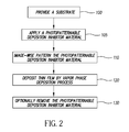
- Such a process for forming a patterned thin film comprises:
- metal oxides and other materials can be selectively deposited.
- the present invention relates to forming patterned thin films using selective area deposition (SAD).
- SAD selective area deposition
- Various methods of vapor phase deposition for depositing the thin films can be used, for example, chemical vapor deposition (CVD) or atomic layer deposition (ALD).
- Selective area deposition as noted above involves treating portion(s) of a substrate such that a material is deposited only in those areas that are desired.
- the present invention employs a photopatternable deposition inhibitor material that inhibits the deposition of the thin films on its surface. In this manner, portions of the substrate where there is a deposition inhibitor material will have little to no thin film growth, and in areas of the substrate which are generally free of the inhibitor material will have normal film growth.
- deposit inhibitor material refers herein to the material applied to the substrate as well as the material resulting from any optionally subsequent crosslinking or other reaction that modifies the material that may occur prior to depositing an inorganic thin film on the substrate by a vapor phase deposition process.
- the present invention is directed to the use, as a photopatternable deposition inhibitor material, of organosiloxanes and formulations containing organosiloxanes.
- organosiloxanes are defined generically to include compounds substantially comprising, within their chemical structure, a skeleton or moiety made up of alternate Si and O atoms, in which at least one, preferably two organic groups are attached to the Si atom on either side of the -O-Si-O- repeat units.
- the organic groups can have various substituents such as halogens, including fluorine.
- the organic groups are independently substituted or unsubstituted alkyl, phenyl, or cycloalkyl groups having 1 to 6 carbon atoms, preferably 1 to 3 carbon atoms, preferably substituted or unsubstituted methyl.
- Organosiloxane polymers are defined to include polymers, prepolymers, or macromonomers. Particularly preferred are deposition inhibitor materials that, after application onto the substrate, and any crosslinking or intermolecular reaction, are insoluble. Such organosiloxane polymers include random or block and/or crosslinked polymers. Crosslinking can be used to insolubilize the organosiloxane polymer after application onto the surface of the substrate. The crosslinking may occur during patterning in order to contribute to the patterning step, for example, by employing crosslinking initiated by, and patterned by, actinic radiation, followed by removal of non-crosslinked polymer, for example, by solvent.
- functional groups may be present on the organosiloxane polymer such as terminal groups (also referred to as endcaps).
- Terminal groups also referred to as endcaps.
- Crosslinking groups, and/or functional groups may also be present, for example, located on a side chain off a siloxane backbone.
- organosiloxane polymers include, for example, poly(alkylsiloxane), poly(arylsiloxane), poly(alkylarylsiloxane), and poly(alkyl(aryl)siloxane), optionally having functional groups.
- functionalized poly(siloxanes) include epoxy-functionalized, carboxyl-functionalized, polyether-functionalized, phenol-functionalized, amino-functionalized, alkoxy-functionalized, methacryl-functionalized, carbinol-functionalized, hydroxy-functionalized, vinyl-functionalized, acrylic-functionalized, silane-functionalized, trifluoro-functionalized, or mercapto-functionalized poly(organosiloxanes).
- Block copolymers can also be employed if at least one of the blocks contains substantial siloxane repeat units.
- Such polymers can be prepared as described in numerous patents and publications or are commercially available from, for example, General Electric, Dow Corning, and Petrarch.
- the preferred poly(organosiloxane) polymers comprise organic groups (attached to the silicon atoms) that are independently hydrogen, alkyl having from 1 to 18 carbons, such as methyl, ethyl, propyl, and butyl, an aryl group having 6 to 18 carbons, preferably 6 to 8 carbon atoms, such as phenyl, benzyl, and napthyl, a mercaptoalkyl group having from 1 to 18 carbons, such as mercaptopropyl; an aminoalkyl group having from 1 to 18 carbons, such as aminopropyl or aminoisopropyl; trifluoroalkyl having 1 to 18 carbons, such as trifluoromethyl; or trifluoroaryl having 6 to 18 carbons, such as trifluoromethylphenyl.
- the preferred weight average molecular weight range for the poly(organosiloxane) polymers, if not crosslinked, is 200 to 140,000, more preferably 4,000 to 120,000.
- alkyl groups have 1 to 6 carbon atoms, more preferably 1 to 3 carbon atoms.
- Some preferred illustrative poly(organosiloxane) polymers are poly(dimethylsiloxane), poly(diphenylsiloxane), poly(methylphenylsiloxane), poly(dimethyldiphenylsiloxane), mercaptopropylfunctionalized poly(dimethylsiloxane), aminopropyl-functionalized poly(dimethylsiloxane), carboxypropyl-functionalized poly(dimethylsiloxane), silane-functionalized poly(dimethylsiloxane), and trifluoropropyl-functionalized poly(dimethylsiloxane).
- More preferred poly(organosiloxane) polymers are poly(dimethylsiloxane) (PDMS) and poly(dimethyldiphenylsiloxane), that is, where the organic groups are appropriately methyl or phenyl. Mixtures of poly(organosiloxane) polymers or compounds can be used. As indicated below, the organosiloxane can be mixed with other polymers as appropriate to the task.
- Organosiloxanes for use in selective area deposition can provide near zero growth of the thin film on the inhibitor surface. This property greatly enhances the usefulness of the deposition inhibitor material, since it enables a thin film to be selectively deposited that is of a much greater thickness than those previously capable of being deposited in SAD processes.
- a patterned thin film is deposited via a vapor phase deposition process, such as ALD, and simultaneously patterned using selective area deposition (SAD) materials and processes.
- SAD processes use a deposition inhibitor compound in order to inhibit the ALD growth of the thin film in the non-selected areas.
- ALD can be used as a fabrication step for forming a number of types of thin-films for electronic devices, including semiconductor devices and supporting electronic components such as resistors and capacitors, insulators, bus lines, and other conductive structures.
- ALD is particularly suited for forming thin layers of metal oxides in the components of electronic devices.
- General classes of functional materials that can be deposited with ALD include conductors, dielectrics or insulators, and semiconductors.
- ALD steps are self-terminating and can deposit precisely one atomic layer when conducted up to or beyond self-termination exposure times.
- An atomic layer typically ranges from 0.1 to 0.5 molecular monolayers, with typical dimensions on the order of no more than a few Angstroms.
- deposition of an atomic layer is the outcome of a chemical reaction between a reactive molecular precursor and the substrate.
- the net reaction deposits the desired atomic layer and substantially eliminates "extra" atoms originally included in the molecular precursor.
- ALD involves the adsorption and reaction of each of the precursors in the complete absence of the other precursor or precursors of the reaction.
- a metal precursor molecule typically comprises a metal element, M that is bonded to an atomic or molecular ligand, L.
- M could be, but would not be restricted to, Al, W, Ta, Si, Zn, etc.
- the metal precursor reacts with the substrate when the substrate surface is prepared to react directly with the molecular precursor.
- the substrate surface typically is prepared to include hydrogen-containing ligands, or AH that are reactive with the metal precursor. Sulfur (S), oxygen (O), and Nitrogen (N) are some typical A species.
- the gaseous precursor molecule effectively reacts with all of the ligands on the substrate surface, resulting in deposition of a single atomic layer of the metal: substrate-AH+ML x ⁇ substrate-AML x-1 +HL (1) where HL is a reaction by-product.
- HL is a reaction by-product.
- the initial surface ligands, AH are consumed, and the surface becomes covered with AML x-1 ligands, which cannot further react with metal precursor ML x . Therefore, the reaction self-terminates when all of the initial AH ligands on the surface are replaced with AML x-1 species.
- the reaction stage is typically followed by an inert-gas purge stage that eliminates the excess metal precursor and the HL by-product species from the chamber prior to the separate introduction of the other precursor.
- a second molecular precursor then is used to restore the surface reactivity of the substrate towards the metal precursor. This is done, for example, by removing the L ligands and re-depositing AH ligands.
- the second precursor typically comprises the desired (usually nonmetallic) element A (i.e., O, N, S), and hydrogen (i.e., H 2 O, NH 3 , H 2 S).
- desired element A i.e., O, N, S
- hydrogen i.e., H 2 O, NH 3 , H 2 S
- an ALD process requires alternating in sequence the flux of chemicals to the substrate.
- the representative ALD process as discussed above, is a cycle having four different operational stages:
- ALD deposition cycle This repeated sequence of alternating surface reactions and precursor-removal that restores the substrate surface to its initial reactive state, with intervening purge operations, is a typical ALD deposition cycle.
- a key feature of ALD operation is the restoration of the substrate to its initial surface chemistry condition.
- a film can be layered onto the substrate in equal metered layers that are all identical in chemical kinetics, deposition per cycle, composition, and thickness.
- Self-saturating surface reactions make ALD insensitive to transport non-uniformities, which might otherwise impair surface uniformity, due either to engineering tolerances and the limitations of the flow process or related to surface topography (that is, deposition into three dimensional, high aspect ratio structures).
- a non-uniform flux of chemicals in a reactive process generally results in different completion times at different areas.
- each of the reactions is allowed to complete on the entire substrate surface.
- differences in completion kinetics impose no penalty on uniformity. This is because the areas that are first to complete the reaction self-terminate the reaction; other areas are able to continue until the full treated surface undergoes the intended reaction.
- an ALD process deposits 0.1 - 0.2 nm of a film in a single ALD cycle (with numbered steps 1 through 4 as listed earlier).
- a useful and economically feasible cycle time must be achieved in order to provide a uniform film thickness in a range of from 3 nm to 300 nm for many or most semiconductor applications, and even thicker films for other applications.
- Industry throughput standards dictate that substrates be processed in 2 minutes to 3 minutes, which means that ALD cycle times must be in a range from 0.6 seconds to 6 seconds.
- An ALD process must be able to execute this sequencing efficiently and reliably for many cycles in order to allow cost-effective coating of many substrates.
- pulsed ALD process a substrate sits in a chamber and is exposed to the above sequence of gases by allowing a first gas to enter the chamber, followed by a pumping cycle to remove that gas, followed by the introduction of a second gas to the chamber, followed by a pumping cycle to remove the second gas.
- This sequence can be repeated at any frequency and variations in gas type and/or concentration.
- the net effect is that the entire chamber experiences a variation in gas composition with time, and thus this type of ALD can be referred to as time dependent ALD.
- the vast majority of existing ALD processes are time dependent ALD.
- each reactant gas can be provided continuously while moving the substrate through each gas in succession.
- a relatively constant gas composition exists, but is located to specific areas or spaces of the processing system.
- These systems can be referred to as spatially dependent ALD systems.
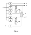
- US Patent No. 6,821,563 entitled “GAS DISTRIBUTION SYSTEM FOR CYCLICAL LAYER DEPOSITION” to Yudovsky describes a spatially dependent ALD processing system, under vacuum, having separate gas ports for precursor and purge gases, alternating with vacuum pump ports between each gas port. Each gas port directs its stream of gas vertically downward toward a substrate. Walls or partitions separate the gas flows, with vacuum pumps for evacuating gas on both sides of each gas stream.
- Another approach using continuous gas flow spatially dependent ALD is shown in US Patent No. 4,413,022 entitled “METHOD FOR PERFORMING GROWTH OF COMPOUND THIN FILMS" to Suntola et al.
- a gas flow array is provided with alternating source gas openings, carrier gas openings, and vacuum exhaust openings. Reciprocating motion of the substrate over the array effects ALD deposition, without the need for pulsed operation.
- US Patent Publication No. 2005/0084610 to Selitser discloses an atmospheric pressure atomic layer chemical vapor deposition process. Selitser states that extraordinary increases in reaction rates are obtained by changing the operating pressure to atmospheric pressure, which will involve orders of magnitude increase in the concentration of reactants, with consequent enhancement of surface reactant rates.
- a spatially dependent ALD process can be accomplished with other apparatus or systems described in more detail in commonly assigned US Patent Publication No. 2007/0238311 ; US Patent Publication No. 2007/0228470 ; US Patent Publication No. 2008/0166884 ; and US Patent Application No. 11/620,744 .
- These systems attempt to overcome one of the difficult aspects of a spatial ALD system, which is undesired intermixing of the continuously flowing mutually reactive gases.
- US Patent Publication No. 2007/0238311 employs a novel transverse flow pattern to prevent intermixing
- US Patent Application No. 11/620,744 and US Patent Publication No. 2008/0166884 employ a coating head partially levitated by the pressure of the reactive gases of the process to accomplish improved gas separation.
- ALD is a preferred method of depositing a layer of functional material
- other conventional methods of vapor phase deposition can be used, as will be appreciated by the skilled artisan.
- Figure 1A shows a substrate 200 prior to the application of the deposition inhibitor material 210.
- the substrate 200 is illustrated as a bare substrate, one skilled in the art should recognize that substrate 200 might contain layers of materials, either patterned or unpatterned, to serve any purpose electrical, optical, or mechanical, as desired.
- Figure 1B shows a substrate 200 after a uniform deposition of deposition inhibitor material 210.
- Figure 1C illustrates substrate 200 after the step of patterning the deposition inhibitor material 210 into deposition mask 225. The patterning can be done by any method known in the art, including photolithography using either positive or negative acting photoresists, laser ablation, or other subtractive processes.
- deposition mask 225 contains areas of deposition inhibitor material 210 and areas devoid of deposition inhibitor 215.
- Figure 1D illustrates substrate 200 after the step of atomic layer deposition of the desired thin film material.
- thin film material 220 is only deposited on the substrate 200 where there was no deposition inhibitor material 210.
- the thin film material 220 does not form any appreciable thin film over deposition inhibitor material 210.
- Figure 1E illustrates a patterned thin film material 220 after removing the deposition inhibitor material 210. It should be understood by one skilled in the art, that in some instances it would not be necessary to remove the deposition inhibitor material 210.
- FIG. 2 is a step diagram for one embodiment of a process of the present invention for making a patterned thin film using a combination of selected area deposition (SAD) and ALD.
- a substrate is supplied into the system.
- a photopatternable deposition inhibitor material is deposited.
- the photopatternable deposition inhibitor material can generically be any material that causes the material deposition to be inhibited which can be patterned using light.
- the photopatternable deposition inhibitor material is chosen specifically for the material to be deposited.
- the deposition inhibitor material has a given inhibition power; the inhibition power is defined as the layer thickness at or below which the deposition inhibitor material is effective.
- the photopatternable deposition inhibitor material is chosen to be sensitive only to selected wavelengths of visible light.
- Step 105 deposits a uniform layer of the photopatternable deposition inhibitor material and Step 110 is employed to form a patterned layer of the deposition inhibitor material.
- Step 110 comprises the step of exposing the photopatternable deposition inhibitor material to a pattern of light. The exposing can be done using a large source through a traditional mask or color mask, alternatively, the photopatternable deposition inhibitor material may be exposed using a laser marking system. For mask exposure, the mask may be in contact with substrate or focused through a lens to the substrate. A mask exposure may be done a single time for an entire substrate, or the mask may be stepped over the substrate to achieve several exposures.
- Step 110 also includes the step of developing the photopatternable deposition inhibitor material such that substrate has areas where there is no deposition inhibitor material and areas where the deposition inhibitor material remains.
- Step 120 deposits the desired thin film by a vapor phase deposition process.
- the vapor phase deposition process is an Atomic Layer Deposition (ALD) process.
- ALD Atomic Layer Deposition
- the thin film is deposited only in the areas of the substrate where there is no deposition inhibitor material.
- the deposition inhibitor material may remain on the substrate for subsequent processing or may be removed as shown in Step 130 of Figure 2 .
- the present invention utilizes a photopatternable deposition inhibitor material that contains an organosiloxane.
- the photopatternable deposition inhibitor also contains a sensitizer.
- the deposition inhibitor material of the present invention preferably has an effective inhibition power, defined as the functional layer thickness at or below which the deposition inhibitor material is effective.
- the deposition inhibitor material during use, exhibits an inhibition power of at least 50 ⁇ , more preferably at least 100 ⁇ , most preferably at least 300 ⁇ .
- the organosiloxane can be crosslinked or photopolymerized after being applied.
- Crosslinking can be used to insolubilize a polymeric deposition inhibitor material after application onto the surface of the substrate.
- the crosslinking can occur during patterning in order to contribute to the patterning step, for example, by employing crosslinking initiated by, and patterned by, exposing the photopatternable deposition inhibitor, followed by removal of non-crosslinked polymer, for example, by solvent.
- the deposition inhibitor material in addition to the organosiloxane also contains a photopatternable material, for example, a photopolymerizable or photosolubilizable (or "photosolulizable") material, in combination with a sensitizing system, the combination referred to as a photopolymerization system, which can be blended with organosiloxane to obtain the deposition inhibitor material.
- a photopatternable material for example, a photopolymerizable or photosolubilizable (or "photosolulizable" material, in combination with a sensitizing system, the combination referred to as a photopolymerization system, which can be blended with organosiloxane to obtain the deposition inhibitor material.
- the sensitizing system for the photopolymerization system for providing sensitivity to visible light, can be accomplished by the use of, along with a polymerizable compound, a photopolymerization initiator.
- the photopatternable material for the photopatternable deposition inhibitor material contains a polymerizable compound selected from among compounds having at least one, preferably two or more, ethylenically unsaturated bonds.
- Such compounds are well known in the industry and they can be used in the present invention with no particular limitation.
- Such compounds have, for example, the chemical form of a monomer, a prepolymer, i.e., a dimer, a trimer, and an oligomer or a mixture and a copolymer of them.
- unsaturated carboxylic acids e.g., acrylic acid, methacrylic acid, itaconic acid; crotonic acid, isocrotonic acid, maleic acid, etc.
- esters and amides thereof can be exemplified, and preferably esters of unsaturated carboxylic acids and aliphatic polyhydric alcohol compounds, and amides of unsaturated carboxylic acids and aliphatic polyhydric amine compounds are used.
- the addition reaction products of unsaturated carboxylic esters and amides having a nucleophilic substituent such as a hydroxyl group, an amino group and a mercapto group with monofunctional or polyfunctional isocyanates and epoxies, and the dehydration condensation reaction products of these compounds with monofunctional or polyfunctional carboxylic acids are also preferably used.
- ester monomers of aliphatic polyhydric alcohol compounds and unsaturated carboxylic acids include, as acrylates, ethylene glycol diacrylate, triethylene glycol diacrylate, 1,3- butanediol diacrylate, tetramethylene glycol diacrylate, propylene glycol diacrylate, neopentyl glycol diacrylate, trimethylolpropane triacrylate, trimethylolpropane tri(acryloyloxypropyl)ether, trimethylolethane triacrylate, hexanediol diacrylate, 1,4-cyclohexanediol diacrylate, tetraethylene glycol diacrylate, pentaerythritol diacrylate, pentaerythritol triacrylate, pentaerythritol tetraacrylate, dipentaerythritol diacrylate, dipentaerythritol hexaacrylate, sorbitol tri
- examples include tetramethylene glycol dimethacrylate, triethylene glycol dimethacrylate, neopentyl glycol dimethacrylate, trimethylolpropane trimethacrylate, trimethylolethane trimethacrylate, ethylene glycol dimethacrylate, 1,3- butanediol dimethacrylate, hexanediol dimethacrylate, pentaerythritol dimethacrylate, pentaerythritol trimethacrylate, pentaerythritol tetramethacrylate, dipentaerythritol dimethacrylate, dipentaerythritol hexamethacrylate, sorbitol trimethacrylate, sorbitol tetramethacrylate, and bis[p-(3-methacryloxy-2-hydroxypropoxy)phenyl]dimethylmethane, bis[p- (methacryloxy-2-hydroxy
- examples include ethylene glycol diitaconate, propylene glycol diitaconate, 1,3-butanediol diitaconate, 1,4-butanediol diitaconate, tetramethylene glycol diitaconate, pentaerythritol diitaconate, and sorbitol tetraitaconate.
- examples include ethylene glycol dicrotonate, tetramethylene glycol dicrotonate, pentaerythritol dicrotonate, and sorbitol tetradicrotonate.
- examples include ethylene glycol diisocrotonate, pentaerythritol diisocrotonate, and sorbitol tetraisocrotonate.
- examples include ethylene glycol dimaleate, triethylene glycol dimaleate, pentaerythritol dimaleate, and sorbitol tetramaleate. Further, the mixtures of the above-described ester monomers can also be used.
- amide monomers of aliphatic polyhydric amine compounds and unsaturated carboxylic acids include methylenebis acrylamide, methylenebismethacrylamide, 1,6-hexamethylenebis- acrylamide, 1,6-hexamethylenebismethacrylamide, diethylenetriaminetris- acrylamide, xylylenebis-acrylamide, and xylylenebis-methacrylamide.
- urethane-based addition polymerizable compounds which are obtained by the addition reaction of an isocyanate and a hydroxyl group can also be used in the photopatternable material for the photopatternable deposition inhibitor material.
- a specific example is a vinyl urethane compound having two or more polymerizable vinyl groups in one molecule, which is obtained by the addition of a vinyl monomer having a hydroxyl group represented by the following formula (V) to a polyisocyanate compound having two or more isocyanate groups in one molecule.
- CH 2 C(R)COOCH 2 CH(R')OH wherein R and R' each represents H or CH 3 .
- polyfunctional acrylates and methacrylates such as polyester acrylates, and epoxy acrylates obtained by reacting epoxy resins with (meth)acrylic acids.
- photo-curable monomers and oligomers listed in Sartomer Product Catalog by Sartomer Company Inc. (1999 ) can be used as well.
- a suitable addition polymerizable compound or combination of addition polymerizable compounds having the desired structure and amounts can be used.
- the conditions are selected from the following viewpoint.
- a structure containing many unsaturated groups per molecule is preferred and in many cases bifunctional or more functional groups are preferred.
- bifunctional or more functional groups are preferred.
- trifunctional or more functional groups are preferred. It is effective to use different functional numbers and different polymerizable groups (e.g., acrylate, methacrylate, styrene compounds, vinyl ether compounds) in combination to control both photosensitivity and strength.
- Compounds having a large molecular weight or compounds having high hydrophobicity are excellent in photosensitive speed and film strength, but may not be preferred from the point of development speed and precipitation in a developing solution.
- the selection and usage of the addition polymerizable compound are important factors for compatibility with other components in the photopatternable deposition inhibitor material (e.g., the organosiloxane, any additional binder polymer, an initiator, etc.) and incompatibility with a subsequently applied functional material. For example, sometimes compatibility can be improved by using a low purity compound or two or more compounds in combination. Further, it is also possible to select a compound having specific structure for the purpose of improving the adhesion property to the support.
- the addition-polymerizable compound may be used alone or in combination of two or more.
- appropriate structure, compounding ratio and addition amount of the addition-polymerizable compound can be arbitrarily selected taking into consideration the degree of polymerization hindrance due to oxygen, resolving power, fogging characteristic, refractive index variation and surface adhesion.
- Organic polymeric binders which can optionally form a part of the film forming component of the photopatternable layer include: (1) polyesters, including those based on terephthalic, isophthalic, sebacic, adipic, and hexahydroterephthalic acids; (2) nylons or polyamides; (3) cellulose ethers and esters; (4) polyaldehydes; (5) high molecular weight ethylene oxide polymers-e.g., poly(ethylene glycols), having average weight average molecular weights from 4000 to 4,000,000; (6) polyurethanes; (7) polycarbonates; (8) synthetic rubbers - e.g., homopolymers and copolymers of butadienes; and (9) homopolymers and copolymers formed from monomers containing ethylenic unsaturation such as polymerized forms of any of the various ethylenically unsaturated monomers, such as polyalkylenes - e.g.
- polyethylene and polypropylene poly(vinyl alcohol); polystyrene; poly(acrylic and methacrylic acids and esters)-e.g. poly(methyl methacrylate) and poly(ethyl acrylate), as well as copolymer variants.
- the polymerizable compound and the polymeric binder can be employed together in widely varying proportions, including polymerizable compound ranging from 3-97 percent by weight of the film forming component and polymeric binder ranging from 97-3 percent by weight of the film forming component.
- a separate polymeric binder although preferred, is not an essential part of the photopatternable film and is most commonly omitted when the polymerizable compound is itself a polymer.
- photoinitiators can be selected for use in the above-described photopatternable deposition inhibitor material.
- Preferred photoinitators consist of an organic dye.
- the amount of organic dye to be used is preferably in the range of from 0.1 to 5% by weight based on the total weight of the photopolymerization composition, preferably from 0.2 to 3% by weight.
- the organic dyes for use as photoinitiators may be suitably selected from conventionally known compounds having a maximum absorption wavelength falling within a range of 300 to 1000 nm. High sensitivity can be achieved by selecting a desired dye having a desired absorption spectrum. Also, it is possible to suitably select a light source such as blue, green, or red, or infrared LED (light emitting diode), solid state laser, OLED (organic light emitting diode) or laser, for use in image-wise exposure to light.
- a light source such as blue, green, or red, or infrared LED (light emitting diode), solid state laser, OLED (organic light emitting diode) or laser, for use in image-wise exposure to light.
- the photoinitiator organic dyes include 3-ketocoumarin compounds, thiopyrylium salts, naphthothiazolemerocyanine compounds, merocyanine compounds, and merocyanine dyes containing thiobarbituric acid, hemioxanole dyes, and cyanine, hemicyanine, and merocyanine dyes having indolenine nuclei.
- Other examples of the organic dyes include the dyes described in Chemistry of Functional Dyes (1981, CMC Publishing Co., Ltd., pp. 393-416 ) and Coloring Materials (60 [4], 212-224, 1987 ).
- organic dyes include cationic methine dyes, cationic carbonium dyes, cationic quinoimine dyes, cationic indoline dyes, and cationic styryl dyes.
- examples of the above-mentioned dyes include keto dyes such as coumarin dyes (including ketocoumarin and sulfonocoumarin), merostyryl dyes, oxonol dyes, and hemioxonol dyes; nonketo dyes such as nonketopolymethine dyes, triarylmethane dyes, xanthene dyes, anthracene dyes, rhodamine dyes, acridine dyes, aniline dyes, and azo dyes; nonketopolymethine dyes such as azomethine dyes, cyanine dyes, carbocyanine dyes, dicarbocyanine dyes, tricarbocyanine dyes, hemicyanine dyes, and
- the photoinitiator organic dye is a cationic dye-borate anion complex formed from a cationic dye and an anionic organic borate.
- the cationic dye absorbs light having a maximum absorption wavelength falling within a range from 300 to 1000 nm and the anionic borate has four R groups, of which three R groups each represents an aryl group which may have a substitute, and one R group is an alkyl group, or a substituted alkyl group.
- Such cationic dye-borate anion complexes have been disclosed in US Patent Nos. 5,112,752 ; 5,100,755 ; 5, 057,393 ; 4,865,942 ; 4,842,980 ; 4,800,149; 4,772,530 ; and 4,772,541 .
- the cationic dye-borate anion complex When used as the organic dye in the photopolymerization compositions of the invention, it does not require to use the organoborate salt. However, to increase the photopolymerization sensitivity, it is prefered to use an organoborate salt in combination with the cationic dye-borate complex.
- the organic dye can be used singly or in combination.
- the photoinitiator may be preferable to use in combination with an organic borate salt such as disclosed in US Patent Nos. 5,112,752 ; 5,100,755 ; 5,057,393 ; 4,865,942 ; 4,842,980 ; 4,800,149 ; 4, 772,530 and 4,772,541 .
- an organic borate salt such as disclosed in US Patent Nos. 5,112,752 ; 5,100,755 ; 5,057,393 ; 4,865,942 ; 4,842,980 ; 4,800,149 ; 4, 772,530 and 4,772,541 .
- the amount of borate compound contained in the photopolymerization composition of the invention is preferably from 0% to 20% by weight based on the total amount of photopolymerization composition.
- the borate salt useful for the photosensitive composition of the present invention is represented by the following general formula (I).
- Plural Rs may be the same as or different from each other.
- two or more of these groups may join together directly or via a substituent and form a boron-containing heterocycle.
- Z+ does not absorb light and represents an alkali metal, quaternary ammonium, pyridinium, quinolinium, diazonium, morpholinium, tetrazolium, acridinium, phosphonium, sulfonium, oxosulfonium, iodonium, S, P, Cu, Ag, Hg, Pd, Fe, Co, Sn, Mo, Cr, Ni, As, or Se.
- a reducing agent such as an oxygen scavenger or a chain-transfer aid of an active hydrogen donor, or other compound can be used to accelerate the polymerization.
- An oxygen scavenger is also known as an autoxidizer and is capable of consuming oxygen in a free radical chain process. Examples of useful autoxidizers are N,N- dialkylanilines.
- N,N-dialkylanilines are dialkylanilines substituted in one or more of the ortho-, meta-, or para-position by the following groups: methyl, ethyl, isopropyl, t-butyl, 3,4-tetramethylene, phenyl, trifluoromethyl, acetyl, ethoxycarbonyl, carboxy, carboxylate, trimethylsilymethyl, trimethylsilyl, triethylsilyl, trimethylgermanyl, triethylgermanyl, trimethylstannyl, triethylstannyl, n-butoxy, n-pentyloxy, phenoxy, hydroxy, acetyl-oxy, methylthio, ethylthio, isopropylthio, thio-(mercapto-), acetylthio, fluoro, chloro, bromo and iodo.
- N,N-dialkylanilines useful in the present invention are 4-cyano-N,N-dimethylaniline, 4-acetyl-N,N-dimethylaniline, 4-bromo-N,N-dimethylaniline, ethyl 4-(N,N-dimethylamino)benzoate, 3-chloro-N,N-dimethylaniline, 4-chloro-N,N- dimethylaniline, 3-ethoxy-N,N-dimethylaniline, 4-fluoro-N,N-dimethylaniline, 4- methyl-N,N-dimethylaniline, 4-ethoxy-N,N-dimethylaniline, N,N-dimethylaniline, N,N-dimethylthioanicidine 4-amino-N,N-dimethylaniline, 3-hydroxy-N,N- dimethylaniline, N,N,N',N'-tetramethyl-1,4-dianiline, 4-acetamido-N,N-di
- the photoinitiator may be preferable to use in combination with a disulfide coinitiator.
- a disulfide coinitiator examples include mercaptobenzothiazo-2-yl disulfide and 6- ethoxymercaptobenzothiazol-2-yl disulfide.
- thiols, thioketones, trihalomethyl compounds, lophine dimer compounds, iodonium salts, sulfonium salts, azinium salts, organic peroxides, and azides are examples of compunds useful as polymerization accelerators.
- additives which can be incorporated into the photopatternable coatings include polymeric binders, fillers, pigments, surfactants, or adhesion modifiers,
- the light curable film composition is usually dispersed in a solvent to create a solution or slurry, and then the liquid is evaporatively removed, usually with heating, after coating.
- Any solvent can be employed for this purpose which is inert toward the film forming components and addenda of the light curable film.
- Examples of compounds which are known to sensitize onium salts are those in the following classes: diphenylmethane including substituted diphenylmethane, xanthene, acridine, methine and polymethine (including oxonol, cyanine, and merocyanine) dye, thiazole, thiazine, azine, aminoketone, porphyrin, colored aromatic polycyclic hydrocarbon, p-substituted aminostyryl compound, aminotriazyl methane, polyarylene, polyarylpolyene, 2,5-diphenylisobenzofuran, 2,5-diarylcyclopentadiene, diarylfuran, diarylthiofuran, diarylpyrrole, polyarylphenylene, coumarin and polyaryl-2-pyrazoline.
- diphenylmethane including substituted diphenylmethane, xanthene, acridine, methine and polymet
- a mixtures of organosiloxane with a photopolymerizable matrix activated by long UV or visible radiation are preferable photopatternable deposition inhibitor materials.
- Blends of organosiloxanes with cyclized rubber (poly cis -isoprene), sensitized to UV radiation with a bis-azide (such as 2,6-bis (4-azidobenzal)-4-methylcyclohexanone), are particularly preferred photopatternable compositions for use with the present invention.
- These formulations may optionally be sensitized to visible wavelengths in accordance with the present invention.
- the sensitization of poly cis -isoprene resists to visible wavelengths has been described, for example, by J. Frejlich and R. Knoesel (Applied Optics, 18 8 1135-1136 (1979 ), using triplet sensitizers such as 9-fluorenone).
- a layer of photopatternable deposition inhibitor material may be exposed using any convenient method.
- the layer may be exposed using a photomask or may be laser-exposed without a photomask.
- the important aspect of the exposure step is that a light pattern containing appropriate wavelength actinic radiation is provided to the photopatternable deposition inhibitor layer so that desired regions are sufficiently exposed for the photopatternable deposition inhibitor material to transition from soluble to insoluble, or vise versa, while other regions remain in the original as-coated state.
- a photopatternable deposition inhibitor layer can be developed by any means known the art. For example, development can involve removing the soluble portions of photopatternable deposition inhibitor layer. Methods for developing typically include exposure to a selective solvent, heating, or combinations thereof.
- a liquid developer can be any convenient liquid that is capable of selectively removing the light curable layer in uncured areas.
- the exposed photopatternable layer can be sprayed, flushed, swabbed, soaked, sonicated, or otherwise treated to achieve selective removal.
- the liquid developer can be the same liquid employed as a solvent in coating the photopatternable deposition inhibitor material.
- the photopatternable deposition inhibitor material is not rendered soluble where it is ultimately to be removed, but is instead rendered susceptible to a particular reaction that occurs during exposure to a development solution which then permits solubility.
- the photopatterned deposition inhibitor layer In patterning processes where the photopatterned deposition inhibitor layer is not intended to be part of the final article, it needs to be removed after it has been used to successfully pattern an area. This removal can be accomplished with any means known in the art, included plasma treatments, especially plasmas including oxygen, solvent based stripping, and mechanical or adhesive means.
- the process of making the patterned thin film in the present process can be carried out below a maximum support temperature of 300° C, more preferably below 250° C, or even at temperatures around room temperature (25° C to 70°C).
- the temperature selection generally depends on the support and processing parameters known in the art, once one is armed with the knowledge of the present invention contained herein. These temperatures are well below traditional integrated circuit and semiconductor processing temperatures, which enables the use of any of a variety of relatively inexpensive supports, such as flexible polymeric supports. Thus, the process enables production of relatively inexpensive circuits containing thin film transistors with significantly improved performance.
- the present process offers a significant departure from conventional approaches to making thin films that can be adaptable to patterning of thin films on relatively large and web-based substrates and capable of achieving improved throughput speeds.
- the process of the present invention optionally allows operation at atmospheric or near-atmospheric pressures and is capable of operating in an unsealed or open-air environment.
- the functional material that is deposited as a thin film after patterning the deposition inhibitor material includes a variety of inorganic materials that are metals or that comprise a metal-containing compound.
- metal-containing compounds include, for example (with respect to the Periodic Table) a Group V or Group VI anion.
- Such metal-containing compound can, for example, include oxides, nitrides, sulfides or phosphides of zinc, aluminum, titanium, hafnium, zirconium or indium, or combinations thereof.
- Metals include, for example, copper, tungsten, aluminum, nickel, ruthenium, or rhodium.
- Oxides that can be made using the process include, but are not limited to: zinc oxide (ZnO), aluminum oxide (Al 2 O 3 ), hafnium oxide, zirconium oxide, indium oxide, and tin oxide,
- Mixed structure oxides that can be made using the process of the present invention can include, for example, InZnO.
- Doped materials that can be made using the process of the present invention can include, for example, ZnO:Al, Mg x Zn 1-x O, and LiZnO.
- Metals that can be made using the process include, but are not limited to: copper, tungsten, aluminum, nickel, ruthenium, and/or rhodium. It will be apparent to the skilled artisan that alloys of two, three, or more metals may be deposited, compounds may be deposited with two, three, or more constituents, and such things as graded films and nano-laminates may be produced as well.
- a given area of the substrate, on which the photopatternable deposition inhibitor material has bee applied is exposed to a gas flow for less than 500 milliseconds, preferably less than 100 milliseconds.
- the temperature of the substrate during deposition is under 300°C, more preferably under 250°C.
- each O-M cycle formed a layer of one atomic diameter over 1 ⁇ 4 of the treated surface.
- four cycles in this case, are needed to form a uniform layer of 1 atomic diameter over the treated surface.
- 40 cycles would be required.
- the flow setup is supplied with nitrogen gas flow 81 that has been purified to remove oxygen and water contamination to below 1 ppm.
- the gas is diverted by a manifold to several flow meters which control flows of purge gases and of gases diverted through bubblers to select the reactive precursors.
- air flow 90 is also delivered to the apparatus. The air is pretreated to remove moisture.
- metal precursor flow 92 containing metal precursors diluted in nitrogen gas
- oxidizer-containing flow 93 containing non-metal precursors or oxidizers diluted in nitrogen gas
- nitrogen purge flow 95 composed only of the inert gas.
- the composition and flows of these streams are controlled as described below.
- Gas bubbler 82 contains liquid diethylzinc (DEZ).
- Flow meter 85 delivers flows of pure nitrogen to the diethylzinc bubbler 82.
- the output of the bubbler 82 now contains nitrogen gas saturated with the respective precursor solution.
- Gas bubbler 83 contains liquid dimethylaluminum isopropoxide (DMAI).
- Flow meter 86 delivers flows of pure nitrogen to the dimethylaluminum isopropoxide bubbler 83.
- the output of the bubbler 83 now contains nitrogen gas saturated with the respective precursor solution.
- the output flow of the DMAI and DEZ bubblers is mixed with a nitrogen gas dilution flow delivered from flow meter 87 to yield the overall flow of metal precursor flow 92.
- the flows will be as follows:
- Gas bubbler 84 contains pure water at room temperature.
- Flow meter 88 delivers a flow of pure nitrogen to gas bubbler 84, the output of which represents a stream of saturated water vapor.
- An airflow is controlled by flow meter 91.
- the water bubbler output and air streams are mixed with dilution stream from flow meter 89 to produce the overall flow of oxidizer-containing flow 93 which has a variable water vapor composition, nitrogen composition, and total flow.
- the flows will be as follows:
- Flow meter 94 controls the flow of pure nitrogen that is to be delivered to the coating apparatus.
- Streams or Flows 92, 93, and 95 are then delivered to an atmospheric pressure coating head where they are directed out of the channels or microchamber slots as indicated in Figure 3 .
- a gap 99 of approximately 0.15 mm 30 microns exists between the elongated channels and the substrate 97.
- the microchambers are approximately 2.5 mm tall, 0.86 mm wide, and run the length of the coating head which is 76 mm.
- the reactant materials in this configuration are delivered to the middle of the slot and flow out of the front and back.
- the delivery head In order to perform a deposition, the delivery head is positioned over a portion of the substrate 97 and then moved in a reciprocating fashion over the substrate 97, as represented by the arrow 98.
- the length of the reciprocation cycle was 32 mm.
- the rate of motion of the reciprocation cycle is 30 mm/sec.
- DEHESIVE 944 is a vinyl-terminated dimethylsiloxane polymer supplied by Wacker Chemie AG.
- Crosslinker V24 is a methylhydrogenpolysiloxane supplied by Wacker.
- Catalyst OL is an organoplatinum complex in polydimethylsiloxane, also supplied by Wacker.
- Crosslinker V24 and Catalyst OL are used for additional curing of vinyl-terminated siloxane polymers such as DEHESIVE 944.
- PMMA is a poly(methyl methacrylate) based positive working photoresist supplied by MicroChem.
- HNR-80 Waycoat Negative Resist Developer (WNRD), and OCG Rinse 1 were obtained from Fujifilm Electronic Materials.
- HNR-80 is a UV-sensitive negative photoresist, containing cyclized rubber (poly(cis-isoprene)) as a photocrosslinkable material dispersed in a mixture of xylene and ethylbenzene.
- WNRD is a xylene free developer for polyisoprene based negative resists, and was used as a developer for HNR-80 formulations.
- OCG Rinse 1 primarily containing butyl acetate, was used as the rinse for HNR-80 formulations following the development step.
- the relative photosensitivity of the photopatternable coatings described below was estimated using nominal radiometer readings with an IL440 Photoresist Radiometer.
- This example describes the preparation of a thin film coating of an Al 2 O 3 layer on a Si wafer substrate, which can be applied over a photopatterned deposition inhibitor material according to the present process.
- the device used to prepare the Al 2 O 3 and ZnO layers has been described in detail in US Patent Application No. 11/627,525 .
- a 2.5X 2.5 inch square (62.5 mm square) Si wafer was positioned on the platen of this device, held in place by a vacuum assist and heated to 200° C.
- the platen with the Si substrate was positioned under the coating head that directs the flow of the active precursor gasses.
- the spacing between the Si wafer substrate and the coating head was adjusted using a micrometer to 30 microns.
- the coating head has isolated channels through which flow: (1) inert nitrogen gas; (2) a mixture of nitrogen, air and water vapor; and (3) a mixture of active metal alkyl vapor (DMAI) in nitrogen.
- the flow rate of the active metal alkyl vapor was controlled by bubbling nitrogen through the pure liquid DMAI contained in an airtight bubbler by means of individual mass flow control meters. Due to the relatively low vapor pressure of DMAI at room temperature the DMAI bubbler and delivery line to the coating head were heated to 60° C. The temperature of the coating head was also maintained at 60° C.
- the flow of water vapor was controlled by adjusting the bubbling rate of nitrogen passed through pure water in a bubbler.
- This example describes the preparation of a thin film coating a ZnO layer on a Si wafer substrate, which can be applied over a photopatterned deposition inhibitor material according to the present process.
- a 2.5X 2.5 inch square (62.5 mm square) Si wafer was positioned on the platen of the ALD device, held in place by a vacuum assist and heated to 200° C.
- the platen with the Si substrate was positioned under the coating head that directs the flow of the active precursor gasses.
- the spacing between the Si wafer substrate and the coating head was adjusted using a micrometer to 30 microns.
- the coating head has isolated channels through which flow: (1) inert nitrogen gas; (2) a mixture of nitrogen, air, and water vapor; and (3) a mixture of active metal alkyl vapor (Diethyl zinc, DEZ) in nitrogen.
- the flow rate of the active metal alkyl vapor was controlled by bubbling nitrogen through the pure liquid DEZ contained in an airtight bubbler by means of individual mass flow control meters.
- the flow of water vapor was controlled by adjusting the bubbling rate of nitrogen passed through pure water in a bubbler. Adjusting the flow rates of the individual gasses to the settings shown in Table 1, for Example 2 below, the coating process was initiated by oscillating the coating head across the substrate for the number of cycles specified.
- the finished coating was a completely uniform deposit of ZnO having an average thickness of 565 ⁇ .
- a thin film coating of a patterned Al 2 O 3 layer (Sample 2) was prepared, comprised of a Si wafer substrate, a patterned layer of a SAD polymer, a 1100 ⁇ thick Al 2 O 3 dielectric layer that is deposited in the areas that the SAD polymer does not cover.
- the patterned layer of a deposition inhibition polymer was prepared according the following steps:
- the substrate with a patterned layer of deposition inhibition polymer was then subjected to Al 2 O 3 deposition.
- the patterned Al 2 O 3 coating is prepared identically to that procedure in Example 1 above.
- the finished patterned coating appeared as a sharp gridline pattern of Al 2 O 3 lines.
- the deposition was highly selective, the sensitivity of this photopatternable deposition inhibitor formulation was approximately 3400 mJ/cm 2 at 250 nm, too low in effective sensitivity for practical manufacture of patterned coatings.
- This example for comparison to the present process, describes a photopatternable material that does not contain organosiloxane.
- Half of a Si wafer was taped off by scotch tape, and HNR-80 photoresist was spun onto the untaped half. The tape was removed, and the photoresist coating was exposed and developed according to manufacturers recommendations. The taped side was wiped with methanol to remove tape residue (the photoresist coated side was not wiped).
- the substrate with a patterned layer of deposition inhibition polymer was then subjected to Al 2 O 3 deposition.
- the patterned Al 2 O 3 coating is prepared identically to that procedure in Example 1 above.
- the photoresist had only a slight capability to inhibit deposition of alumina.
- the inhibition power is defined as the layer thickness at or below which there is substantially no thin film formed on the deposition inhibitor surface.
- the sensitivity of this photoresist of only ⁇ 100 mJ/cm 2 was substantially better than the photopatternable material described in Comparative Example 3.
- the inhibition power of this photopatternable coating was only 120 ⁇ , too thin for many typical applications.
- a photopatternable deposition inhibitor coating sensitive to blue light was prepared in the following manner.
- a 0.1% solution of Photoinitiator A (Table 3 below) in anisole was prepared.
- a dehesive solution was prepared that contained 1.08% DEHESIVE 944, 0.002% Crosslinker V24, and 0.06% Catalyst OL in a mixture of 33 parts toluene and 48 parts heptane, and 0.85 g of toluene.
- a stock solution was prepared that contained 3.3 g of a 1% solution of polymethylmethacrylate dissolved in toluene, 0.5 g of a 10% solution of TMPTA in toluene, 0.24 g of the photoinitiator solution, and 0.85 g of toluene. To this solution, 0.5 g of the dehesive solution was added. One gram of this stock solution was diluted with 5 g of toluene. The solution was spin coated at 2000 RPM, baked at 80° C for one minute, exposed using blue light, and developed using MIBK, forming a negative resist image.
- a photopatternable coating is prepared in the same way as for Example 4, with the exception that an organosiloxane is added to the coating solution, and the resulting coating is exposed to a pattern of UV light, and developed.
- An alumina layer is selectively deposited over the photopatterned deposition inhibitor material.
- a dehesive solution was prepared containing 0.108% DEHESIVE 944, 0.0002% Crosslinker V24, and 0.006% Catalyst OL in a mixture of 33 parts toluene and 48 parts heptane.
- a coating solution was prepared that contained 1.25 g of HNR-80, 23.75 g of toluene, and 0.5 g of the dehesive solution.
- the resulting solution was spin coated at 2000 RPM for 1 minute, baked at 90° C for 1 minute, exposed with a pattern of UV light, developed in WNRD, and rinsed with OCG Rinse.
- the substrate with a photopatterned layer of deposition inhibition polymer was then subjected to Al 2 O 3 deposition.
- the patterned Al 2 O 3 coating is prepared identically to that procedure in Comparative Example 1 above. Ellipsometry data indicated the photopatterned deposition inhibitor coating had an inhibition power of 750 Angstroms, substantially better than the results from Comparative Example 4.
- a photopatternable deposition inhibitor coating was prepared, exposed, and developed according to the procedure described for Example 6 above, with the exception that visible light sensitizer 9-fluorenone was added to the coating solution and the coating was exposed to a pattern of blue light. 0.04 g of a 1% solution of 9-fluorenone in xylene was added to 5 g of the coating solution used for Example 6. The resulting solution was coated, exposed to a pattern of blue light, and developed using the same procedure as for Example 6. After the photosensitive coating was developed, a zinc oxide coating was selectively deposited on regions not masked by the photopatterned deposition inhibitor, using the same coating device as for Comparative Example 2. Ellipsometry data indicated the photopatternable coating C-12 had an inhibition power of 850 Angstroms.
Landscapes
- Physics & Mathematics (AREA)
- General Physics & Mathematics (AREA)
- Spectroscopy & Molecular Physics (AREA)
- Chemical Vapour Deposition (AREA)
- Electroluminescent Light Sources (AREA)
Applications Claiming Priority (2)
| Application Number | Priority Date | Filing Date | Title |
|---|---|---|---|
| US11/942,780 US7846644B2 (en) | 2007-11-20 | 2007-11-20 | Photopatternable deposition inhibitor containing siloxane |
| PCT/US2008/012632 WO2009067148A1 (en) | 2007-11-20 | 2008-11-10 | Photopatternable deposition inhibitor containing siloxane |
Publications (2)
| Publication Number | Publication Date |
|---|---|
| EP2212747A1 EP2212747A1 (en) | 2010-08-04 |
| EP2212747B1 true EP2212747B1 (en) | 2015-07-22 |
Family
ID=40328571
Family Applications (1)
| Application Number | Title | Priority Date | Filing Date |
|---|---|---|---|
| EP08851109.2A Not-in-force EP2212747B1 (en) | 2007-11-20 | 2008-11-10 | Photopatternable deposition inhibitor containing siloxane |
Country Status (5)
| Country | Link |
|---|---|
| US (1) | US7846644B2 (enExample) |
| EP (1) | EP2212747B1 (enExample) |
| JP (1) | JP2011505588A (enExample) |
| CN (1) | CN101868762B (enExample) |
| WO (1) | WO2009067148A1 (enExample) |
Families Citing this family (30)
| Publication number | Priority date | Publication date | Assignee | Title |
|---|---|---|---|---|
| US20080166880A1 (en) * | 2007-01-08 | 2008-07-10 | Levy David H | Delivery device for deposition |
| US7972898B2 (en) * | 2007-09-26 | 2011-07-05 | Eastman Kodak Company | Process for making doped zinc oxide |
| JP5572447B2 (ja) * | 2010-05-25 | 2014-08-13 | 株式会社日立国際電気 | 半導体装置の製造方法、基板処理方法及び基板処理装置 |
| US8618003B2 (en) | 2011-12-05 | 2013-12-31 | Eastman Kodak Company | Method of making electronic devices using selective deposition |
| KR101941908B1 (ko) * | 2011-12-16 | 2019-01-24 | 후지필름 가부시키가이샤 | 레지스트 박리액 및 레지스트 박리 방법 |
| KR101862547B1 (ko) | 2012-04-13 | 2018-05-31 | 삼성전자주식회사 | 폴리실리콘막 형성 방법 및 반도체 장치의 제조 방법 |
| US8791023B2 (en) * | 2012-08-31 | 2014-07-29 | Eastman Kodak Company | Patterned thin film dielectric layer formation |
| US20140065838A1 (en) * | 2012-08-31 | 2014-03-06 | Carolyn R. Ellinger | Thin film dielectric layer formation |
| US8927434B2 (en) * | 2012-08-31 | 2015-01-06 | Eastman Kodak Company | Patterned thin film dielectric stack formation |
| US8986562B2 (en) | 2013-08-07 | 2015-03-24 | Ultratech, Inc. | Methods of laser processing photoresist in a gaseous environment |
| US9634145B2 (en) | 2014-10-29 | 2017-04-25 | Eastman Kodak Company | TFT substrate with variable dielectric thickness |
| US9368491B2 (en) | 2014-10-29 | 2016-06-14 | Eastman Kodak Company | Enhancement mode inverter with variable thickness dielectric stack |
| US9368490B2 (en) | 2014-10-29 | 2016-06-14 | Eastman Kodak Company | Enhancement-depletion mode inverter with two transistor architectures |
| JP6259023B2 (ja) | 2015-07-20 | 2018-01-10 | ウルトラテック インク | 電極系デバイス用のald処理のためのマスキング方法 |
| US9861974B2 (en) * | 2015-08-31 | 2018-01-09 | GM Global Technology Operations LLC | Film system |
| US10052622B2 (en) * | 2016-02-12 | 2018-08-21 | GM Global Technology Operations LLC | Method of forming a self-cleaning film system |
| US10020327B2 (en) | 2016-06-07 | 2018-07-10 | Eastman Kodak Company | Method for selective thin film deposition |
| CN108063089B (zh) * | 2016-11-08 | 2020-07-17 | 中国科学院微电子研究所 | 一种mos器件原子层沉积原位制备方法 |
| KR102112705B1 (ko) * | 2016-12-09 | 2020-05-21 | 주식회사 원익아이피에스 | 박막 증착 방법 |
| US10754067B2 (en) | 2017-05-18 | 2020-08-25 | GM Global Technology Operations LLC | Textured self-cleaning film system and method of forming same |
| US10583428B2 (en) | 2017-05-18 | 2020-03-10 | GM Global Technology Operations LLC | Self-cleaning film system and method of forming same |
| US10556231B2 (en) | 2017-05-18 | 2020-02-11 | GM Global Technology Operations LLC | Self-cleaning film system and method of forming same |
| US10533249B2 (en) * | 2017-05-18 | 2020-01-14 | GM Global Technology Operations LLC | Method of forming a self-cleaning film system |
| US10429641B2 (en) | 2017-05-31 | 2019-10-01 | GM Global Technology Operations LLC | Light-enhanced self-cleaning film system and method of forming same |
| CN109080876B (zh) * | 2017-06-14 | 2023-01-17 | 张家港康得新光电材料有限公司 | 利用保护膜的产品加工方法 |
| KR20210070110A (ko) * | 2019-12-04 | 2021-06-14 | 주성엔지니어링(주) | 전극 형성 방법 |
| CN111769210B (zh) * | 2020-07-14 | 2023-08-08 | 京东方科技集团股份有限公司 | 显示基板及其制备方法、显示装置 |
| CN116351662B (zh) * | 2023-03-31 | 2024-05-17 | 浙江大学 | 一种聚合物薄膜区域选择性沉积的方法 |
| CN116924321A (zh) * | 2023-07-05 | 2023-10-24 | 中国科学院上海微系统与信息技术研究所 | 一种层状结构、制备方法及传感器件 |
| WO2025126882A1 (ja) * | 2023-12-11 | 2025-06-19 | 富士フイルム株式会社 | 組成物、修飾基板の製造方法、積層体の製造方法、電子デバイスの製造方法、化合物 |
Family Cites Families (11)
| Publication number | Priority date | Publication date | Assignee | Title |
|---|---|---|---|---|
| US4284706A (en) | 1979-12-03 | 1981-08-18 | International Business Machines Corporation | Lithographic resist composition for a lift-off process |
| US4394434A (en) * | 1980-12-08 | 1983-07-19 | Minnesota Mining And Manufacturing Company | Plating resist with improved resistance to extraneous plating |
| US4692205A (en) | 1986-01-31 | 1987-09-08 | International Business Machines Corporation | Silicon-containing polyimides as oxygen etch stop and dual dielectric coatings |
| DE69300616T2 (de) * | 1992-04-30 | 1996-05-30 | Ibm | Silikon enthaltendes positives Photoresistmaterial und dessen Verwendung in Dünnfilm-Verpackung-Technologie. |
| JP2000147792A (ja) * | 1998-11-13 | 2000-05-26 | Toyota Central Res & Dev Lab Inc | パターン形成方法 |
| JP3944734B2 (ja) * | 2003-01-10 | 2007-07-18 | 信越化学工業株式会社 | オルガノシロキサン系高分子化合物及び光硬化性樹脂組成物並びにパターン形成方法及び基板保護用皮膜 |
| JP2005274590A (ja) * | 2004-03-22 | 2005-10-06 | Canon Inc | 感光性樹脂組成物及びレジストパターンの形成方法 |
| US7462561B2 (en) * | 2005-01-27 | 2008-12-09 | David Lu | Contact structure formed using supercritical cleaning fluid and ALCVD |
| US20060234499A1 (en) * | 2005-03-29 | 2006-10-19 | Akira Kodera | Substrate processing method and substrate processing apparatus |
| US7160819B2 (en) * | 2005-04-25 | 2007-01-09 | Sharp Laboratories Of America, Inc. | Method to perform selective atomic layer deposition of zinc oxide |
| JP2007178885A (ja) * | 2005-12-28 | 2007-07-12 | Az Electronic Materials Kk | パターンおよび配線パターンならびにそれらの製造法 |
-
2007
- 2007-11-20 US US11/942,780 patent/US7846644B2/en not_active Expired - Fee Related
-
2008
- 2008-11-10 JP JP2010534936A patent/JP2011505588A/ja active Pending
- 2008-11-10 EP EP08851109.2A patent/EP2212747B1/en not_active Not-in-force
- 2008-11-10 CN CN2008801168040A patent/CN101868762B/zh not_active Expired - Fee Related
- 2008-11-10 WO PCT/US2008/012632 patent/WO2009067148A1/en not_active Ceased
Also Published As
| Publication number | Publication date |
|---|---|
| EP2212747A1 (en) | 2010-08-04 |
| JP2011505588A (ja) | 2011-02-24 |
| US20090130608A1 (en) | 2009-05-21 |
| CN101868762A (zh) | 2010-10-20 |
| WO2009067148A1 (en) | 2009-05-28 |
| US7846644B2 (en) | 2010-12-07 |
| CN101868762B (zh) | 2013-03-27 |
Similar Documents
| Publication | Publication Date | Title |
|---|---|---|
| EP2212747B1 (en) | Photopatternable deposition inhibitor containing siloxane | |
| US11705332B2 (en) | Photoresist layer surface treatment, cap layer, and method of forming photoresist pattern | |
| US10437143B2 (en) | Pellicle for exposure to extreme ultraviolet light, photomask assembly, and method of manufacturing the pellicle | |
| US8129098B2 (en) | Colored mask combined with selective area deposition | |
| CN1092244C (zh) | 直接沉积含金属的图案化膜的方法 | |
| US20210397085A1 (en) | Methods for making hard masks useful in next-generation lithography | |
| US20080107878A1 (en) | Colored mask for forming transparent structures | |
| JP2012525000A (ja) | 二重自己整合式金属酸化物薄膜トランジスタ | |
| US6846513B2 (en) | Method for fabricating a silicon thin-film | |
| CN117980833A (zh) | 高分辨率潜像处理、对比度增强和热显影以及用于处理的装置 | |
| US20240355623A1 (en) | Photoresist layer surface treatment, cap layer, and method of forming photoresist pattern | |
| WO2023215136A1 (en) | Post-development treatment of metal-containing photoresist | |
| CN113168093B (zh) | 图案形成方法、感光性树脂组合物、固化膜、层叠体及器件 | |
| TW202338499A (zh) | Euv微影術用之euv活性膜 | |
| WO2009067160A1 (en) | Use of gradient colored mask | |
| CN1272831C (zh) | 细微图案形成方法 | |
| WO2022173632A1 (en) | Quantum efficient photoresists and methods thereof | |
| WO2009067153A1 (en) | Multicolor mask | |
| EP4625043A2 (en) | Tin carboxylate precursors for metal oxide resist layers and related methods | |
| CN118393812B (zh) | 图案化组合物、图案化薄膜、图案化基底、半导体器件及其制备方法 | |
| JP2008021953A (ja) | 回路パターン形成方法 | |
| JP2010049077A (ja) | 膜の剥離方法 |
Legal Events
| Date | Code | Title | Description |
|---|---|---|---|
| PUAI | Public reference made under article 153(3) epc to a published international application that has entered the european phase |
Free format text: ORIGINAL CODE: 0009012 |
|
| 17P | Request for examination filed |
Effective date: 20100510 |
|
| AK | Designated contracting states |
Kind code of ref document: A1 Designated state(s): AT BE BG CH CY CZ DE DK EE ES FI FR GB GR HR HU IE IS IT LI LT LU LV MC MT NL NO PL PT RO SE SI SK TR |
|
| AX | Request for extension of the european patent |
Extension state: AL BA MK RS |
|
| RIN1 | Information on inventor provided before grant (corrected) |
Inventor name: YANG, CHENG Inventor name: IRVING, LYN MARIE Inventor name: LEVY, DAVID HOWARD Inventor name: FREEMAN, DIANE CAROL Inventor name: COWDERY-CORVAN, PETER JEROME |
|
| DAX | Request for extension of the european patent (deleted) | ||
| GRAP | Despatch of communication of intention to grant a patent |
Free format text: ORIGINAL CODE: EPIDOSNIGR1 |
|
| INTG | Intention to grant announced |
Effective date: 20150128 |
|
| GRAS | Grant fee paid |
Free format text: ORIGINAL CODE: EPIDOSNIGR3 |
|
| GRAA | (expected) grant |
Free format text: ORIGINAL CODE: 0009210 |
|
| AK | Designated contracting states |
Kind code of ref document: B1 Designated state(s): AT BE BG CH CY CZ DE DK EE ES FI FR GB GR HR HU IE IS IT LI LT LU LV MC MT NL NO PL PT RO SE SI SK TR |
|
| REG | Reference to a national code |
Ref country code: GB Ref legal event code: FG4D |
|
| REG | Reference to a national code |
Ref country code: CH Ref legal event code: EP |
|
| REG | Reference to a national code |
Ref country code: IE Ref legal event code: FG4D |
|
| REG | Reference to a national code |
Ref country code: AT Ref legal event code: REF Ref document number: 738237 Country of ref document: AT Kind code of ref document: T Effective date: 20150815 |
|
| REG | Reference to a national code |
Ref country code: DE Ref legal event code: R096 Ref document number: 602008039176 Country of ref document: DE |
|
| REG | Reference to a national code |
Ref country code: NL Ref legal event code: FP |
|
| REG | Reference to a national code |
Ref country code: AT Ref legal event code: MK05 Ref document number: 738237 Country of ref document: AT Kind code of ref document: T Effective date: 20150722 |
|
| REG | Reference to a national code |
Ref country code: LT Ref legal event code: MG4D |
|
| PG25 | Lapsed in a contracting state [announced via postgrant information from national office to epo] |
Ref country code: FI Free format text: LAPSE BECAUSE OF FAILURE TO SUBMIT A TRANSLATION OF THE DESCRIPTION OR TO PAY THE FEE WITHIN THE PRESCRIBED TIME-LIMIT Effective date: 20150722 Ref country code: GR Free format text: LAPSE BECAUSE OF FAILURE TO SUBMIT A TRANSLATION OF THE DESCRIPTION OR TO PAY THE FEE WITHIN THE PRESCRIBED TIME-LIMIT Effective date: 20151023 Ref country code: LT Free format text: LAPSE BECAUSE OF FAILURE TO SUBMIT A TRANSLATION OF THE DESCRIPTION OR TO PAY THE FEE WITHIN THE PRESCRIBED TIME-LIMIT Effective date: 20150722 Ref country code: NO Free format text: LAPSE BECAUSE OF FAILURE TO SUBMIT A TRANSLATION OF THE DESCRIPTION OR TO PAY THE FEE WITHIN THE PRESCRIBED TIME-LIMIT Effective date: 20151022 Ref country code: LV Free format text: LAPSE BECAUSE OF FAILURE TO SUBMIT A TRANSLATION OF THE DESCRIPTION OR TO PAY THE FEE WITHIN THE PRESCRIBED TIME-LIMIT Effective date: 20150722 |
|
| PG25 | Lapsed in a contracting state [announced via postgrant information from national office to epo] |
Ref country code: PL Free format text: LAPSE BECAUSE OF FAILURE TO SUBMIT A TRANSLATION OF THE DESCRIPTION OR TO PAY THE FEE WITHIN THE PRESCRIBED TIME-LIMIT Effective date: 20150722 Ref country code: PT Free format text: LAPSE BECAUSE OF FAILURE TO SUBMIT A TRANSLATION OF THE DESCRIPTION OR TO PAY THE FEE WITHIN THE PRESCRIBED TIME-LIMIT Effective date: 20151123 Ref country code: AT Free format text: LAPSE BECAUSE OF FAILURE TO SUBMIT A TRANSLATION OF THE DESCRIPTION OR TO PAY THE FEE WITHIN THE PRESCRIBED TIME-LIMIT Effective date: 20150722 Ref country code: ES Free format text: LAPSE BECAUSE OF FAILURE TO SUBMIT A TRANSLATION OF THE DESCRIPTION OR TO PAY THE FEE WITHIN THE PRESCRIBED TIME-LIMIT Effective date: 20150722 Ref country code: HR Free format text: LAPSE BECAUSE OF FAILURE TO SUBMIT A TRANSLATION OF THE DESCRIPTION OR TO PAY THE FEE WITHIN THE PRESCRIBED TIME-LIMIT Effective date: 20150722 Ref country code: IS Free format text: LAPSE BECAUSE OF FAILURE TO SUBMIT A TRANSLATION OF THE DESCRIPTION OR TO PAY THE FEE WITHIN THE PRESCRIBED TIME-LIMIT Effective date: 20151122 Ref country code: SE Free format text: LAPSE BECAUSE OF FAILURE TO SUBMIT A TRANSLATION OF THE DESCRIPTION OR TO PAY THE FEE WITHIN THE PRESCRIBED TIME-LIMIT Effective date: 20150722 |
|
| REG | Reference to a national code |
Ref country code: DE Ref legal event code: R097 Ref document number: 602008039176 Country of ref document: DE |
|
| PG25 | Lapsed in a contracting state [announced via postgrant information from national office to epo] |
Ref country code: CZ Free format text: LAPSE BECAUSE OF FAILURE TO SUBMIT A TRANSLATION OF THE DESCRIPTION OR TO PAY THE FEE WITHIN THE PRESCRIBED TIME-LIMIT Effective date: 20150722 Ref country code: SK Free format text: LAPSE BECAUSE OF FAILURE TO SUBMIT A TRANSLATION OF THE DESCRIPTION OR TO PAY THE FEE WITHIN THE PRESCRIBED TIME-LIMIT Effective date: 20150722 Ref country code: EE Free format text: LAPSE BECAUSE OF FAILURE TO SUBMIT A TRANSLATION OF THE DESCRIPTION OR TO PAY THE FEE WITHIN THE PRESCRIBED TIME-LIMIT Effective date: 20150722 Ref country code: IT Free format text: LAPSE BECAUSE OF FAILURE TO SUBMIT A TRANSLATION OF THE DESCRIPTION OR TO PAY THE FEE WITHIN THE PRESCRIBED TIME-LIMIT Effective date: 20150722 Ref country code: DK Free format text: LAPSE BECAUSE OF FAILURE TO SUBMIT A TRANSLATION OF THE DESCRIPTION OR TO PAY THE FEE WITHIN THE PRESCRIBED TIME-LIMIT Effective date: 20150722 |
|
| PLBE | No opposition filed within time limit |
Free format text: ORIGINAL CODE: 0009261 |
|
| STAA | Information on the status of an ep patent application or granted ep patent |
Free format text: STATUS: NO OPPOSITION FILED WITHIN TIME LIMIT |
|
| PG25 | Lapsed in a contracting state [announced via postgrant information from national office to epo] |
Ref country code: RO Free format text: LAPSE BECAUSE OF FAILURE TO SUBMIT A TRANSLATION OF THE DESCRIPTION OR TO PAY THE FEE WITHIN THE PRESCRIBED TIME-LIMIT Effective date: 20150722 |
|
| 26N | No opposition filed |
Effective date: 20160425 |
|
| PG25 | Lapsed in a contracting state [announced via postgrant information from national office to epo] |
Ref country code: MC Free format text: LAPSE BECAUSE OF FAILURE TO SUBMIT A TRANSLATION OF THE DESCRIPTION OR TO PAY THE FEE WITHIN THE PRESCRIBED TIME-LIMIT Effective date: 20150722 Ref country code: LU Free format text: LAPSE BECAUSE OF FAILURE TO SUBMIT A TRANSLATION OF THE DESCRIPTION OR TO PAY THE FEE WITHIN THE PRESCRIBED TIME-LIMIT Effective date: 20151110 |
|
| REG | Reference to a national code |
Ref country code: CH Ref legal event code: PL |
|
| PG25 | Lapsed in a contracting state [announced via postgrant information from national office to epo] |
Ref country code: CH Free format text: LAPSE BECAUSE OF NON-PAYMENT OF DUE FEES Effective date: 20151130 Ref country code: LI Free format text: LAPSE BECAUSE OF NON-PAYMENT OF DUE FEES Effective date: 20151130 |
|
| REG | Reference to a national code |
Ref country code: IE Ref legal event code: MM4A |
|
| REG | Reference to a national code |
Ref country code: FR Ref legal event code: ST Effective date: 20160729 |
|
| PG25 | Lapsed in a contracting state [announced via postgrant information from national office to epo] |
Ref country code: SI Free format text: LAPSE BECAUSE OF FAILURE TO SUBMIT A TRANSLATION OF THE DESCRIPTION OR TO PAY THE FEE WITHIN THE PRESCRIBED TIME-LIMIT Effective date: 20150722 |
|
| PG25 | Lapsed in a contracting state [announced via postgrant information from national office to epo] |
Ref country code: IE Free format text: LAPSE BECAUSE OF NON-PAYMENT OF DUE FEES Effective date: 20151110 |
|
| PG25 | Lapsed in a contracting state [announced via postgrant information from national office to epo] |
Ref country code: FR Free format text: LAPSE BECAUSE OF NON-PAYMENT OF DUE FEES Effective date: 20151130 |
|
| PG25 | Lapsed in a contracting state [announced via postgrant information from national office to epo] |
Ref country code: BE Free format text: LAPSE BECAUSE OF FAILURE TO SUBMIT A TRANSLATION OF THE DESCRIPTION OR TO PAY THE FEE WITHIN THE PRESCRIBED TIME-LIMIT Effective date: 20150722 |
|
| PG25 | Lapsed in a contracting state [announced via postgrant information from national office to epo] |
Ref country code: BG Free format text: LAPSE BECAUSE OF FAILURE TO SUBMIT A TRANSLATION OF THE DESCRIPTION OR TO PAY THE FEE WITHIN THE PRESCRIBED TIME-LIMIT Effective date: 20150722 Ref country code: HU Free format text: LAPSE BECAUSE OF FAILURE TO SUBMIT A TRANSLATION OF THE DESCRIPTION OR TO PAY THE FEE WITHIN THE PRESCRIBED TIME-LIMIT; INVALID AB INITIO Effective date: 20081110 |
|
| PG25 | Lapsed in a contracting state [announced via postgrant information from national office to epo] |
Ref country code: CY Free format text: LAPSE BECAUSE OF FAILURE TO SUBMIT A TRANSLATION OF THE DESCRIPTION OR TO PAY THE FEE WITHIN THE PRESCRIBED TIME-LIMIT Effective date: 20150722 |
|
| PG25 | Lapsed in a contracting state [announced via postgrant information from national office to epo] |
Ref country code: TR Free format text: LAPSE BECAUSE OF FAILURE TO SUBMIT A TRANSLATION OF THE DESCRIPTION OR TO PAY THE FEE WITHIN THE PRESCRIBED TIME-LIMIT Effective date: 20150722 Ref country code: MT Free format text: LAPSE BECAUSE OF FAILURE TO SUBMIT A TRANSLATION OF THE DESCRIPTION OR TO PAY THE FEE WITHIN THE PRESCRIBED TIME-LIMIT Effective date: 20150722 |
|
| PGFP | Annual fee paid to national office [announced via postgrant information from national office to epo] |
Ref country code: DE Payment date: 20191017 Year of fee payment: 12 Ref country code: NL Payment date: 20191030 Year of fee payment: 12 |
|
| PGFP | Annual fee paid to national office [announced via postgrant information from national office to epo] |
Ref country code: GB Payment date: 20191029 Year of fee payment: 12 |
|
| REG | Reference to a national code |
Ref country code: DE Ref legal event code: R119 Ref document number: 602008039176 Country of ref document: DE |
|
| REG | Reference to a national code |
Ref country code: NL Ref legal event code: MM Effective date: 20201201 |
|
| GBPC | Gb: european patent ceased through non-payment of renewal fee |
Effective date: 20201110 |
|
| PG25 | Lapsed in a contracting state [announced via postgrant information from national office to epo] |
Ref country code: NL Free format text: LAPSE BECAUSE OF NON-PAYMENT OF DUE FEES Effective date: 20201201 |
|
| PG25 | Lapsed in a contracting state [announced via postgrant information from national office to epo] |
Ref country code: GB Free format text: LAPSE BECAUSE OF NON-PAYMENT OF DUE FEES Effective date: 20201110 Ref country code: DE Free format text: LAPSE BECAUSE OF NON-PAYMENT OF DUE FEES Effective date: 20210601 |