EP2204897B1 - Power converter - Google Patents
Power converter Download PDFInfo
- Publication number
- EP2204897B1 EP2204897B1 EP08843267.9A EP08843267A EP2204897B1 EP 2204897 B1 EP2204897 B1 EP 2204897B1 EP 08843267 A EP08843267 A EP 08843267A EP 2204897 B1 EP2204897 B1 EP 2204897B1
- Authority
- EP
- European Patent Office
- Prior art keywords
- delay
- power converter
- voltage
- switching element
- output
- Prior art date
- Legal status (The legal status is an assumption and is not a legal conclusion. Google has not performed a legal analysis and makes no representation as to the accuracy of the status listed.)
- Active
Links
- 238000005070 sampling Methods 0.000 claims description 7
- 238000005516 engineering process Methods 0.000 description 7
- 238000000034 method Methods 0.000 description 7
- 238000006243 chemical reaction Methods 0.000 description 6
- 238000001514 detection method Methods 0.000 description 6
- 238000010586 diagram Methods 0.000 description 5
- 230000000903 blocking effect Effects 0.000 description 3
- 230000001934 delay Effects 0.000 description 3
- 239000004065 semiconductor Substances 0.000 description 3
- 230000007423 decrease Effects 0.000 description 2
- 230000004048 modification Effects 0.000 description 2
- 238000012986 modification Methods 0.000 description 2
- 230000015572 biosynthetic process Effects 0.000 description 1
- 239000003990 capacitor Substances 0.000 description 1
- 230000000694 effects Effects 0.000 description 1
- 230000001012 protector Effects 0.000 description 1
- 238000007493 shaping process Methods 0.000 description 1
- 230000003068 static effect Effects 0.000 description 1
- 230000007704 transition Effects 0.000 description 1
Images


Classifications
-
- H—ELECTRICITY
- H02—GENERATION; CONVERSION OR DISTRIBUTION OF ELECTRIC POWER
- H02M—APPARATUS FOR CONVERSION BETWEEN AC AND AC, BETWEEN AC AND DC, OR BETWEEN DC AND DC, AND FOR USE WITH MAINS OR SIMILAR POWER SUPPLY SYSTEMS; CONVERSION OF DC OR AC INPUT POWER INTO SURGE OUTPUT POWER; CONTROL OR REGULATION THEREOF
- H02M1/00—Details of apparatus for conversion
- H02M1/08—Circuits specially adapted for the generation of control voltages for semiconductor devices incorporated in static converters
- H02M1/088—Circuits specially adapted for the generation of control voltages for semiconductor devices incorporated in static converters for the simultaneous control of series or parallel connected semiconductor devices
-
- H—ELECTRICITY
- H03—ELECTRONIC CIRCUITRY
- H03K—PULSE TECHNIQUE
- H03K17/00—Electronic switching or gating, i.e. not by contact-making and –breaking
- H03K17/16—Modifications for eliminating interference voltages or currents
- H03K17/168—Modifications for eliminating interference voltages or currents in composite switches
-
- H—ELECTRICITY
- H03—ELECTRONIC CIRCUITRY
- H03K—PULSE TECHNIQUE
- H03K17/00—Electronic switching or gating, i.e. not by contact-making and –breaking
- H03K17/28—Modifications for introducing a time delay before switching
Definitions
- This invention relates to an electric power converter which includes switching circuits having power switching elements such as an IGBT and a MOSFET.
- MOS gate type switching elements including IGBTs and MOSFETs in particular have been increasing their field of applications lately.
- Non-latching type switching elements such as IGBTs and MOSFETs have a significant advantage of high controllability with gate driving as compared to latching type switching elements such as a thyristor.
- Non-latching type switching elements can suppress a surge voltage or surge current according to gate control and can control the gradient of the current and voltage arbitrarily even in the period of switching transition at turn-on and turn-off.
- the multiple series high voltage conversion apparatus is a high voltage conversion apparatus in which a plurality of elements with withstand voltages are connected in series for high voltage applications such as an electric power system.
- the multiple series conversion apparatus has the problem that slight differences in the switching timing between the plurality of elements connected in series can cause large variations in voltage distribution.
- a countermeasure against this is the active gate driving technology (for example, see Jpn. Pat. Appln. Laid-Open Publication No. 2005-86940 ).
- FIG. 7 shows an example of a conventional gate driving circuit that uses the active gate driving technology. More specifically, a switching element 9 in connection with a power line 21 has a control input terminal (or a gate terminal). The gate terminal is connected to a voltage amplifier 2 through a gate resistor 3 and the output terminal of a control current source 6. The input terminal of the control current source 6 is connected to the output terminal of a voltage amplifier 5. The collector-to-emitter voltage of the switching element 9, divided by voltage-dividing resistors 4a and 4b, is applied to the input terminal of the voltage amplifier 5.
- the switching element 9 makes on/off operations according to the gate signal applied through the voltage amplifier 2.
- the output current from the control current source 6 increases.
- the current flowing into the gate terminal of the switching element 9 from the control current source 6 raises the gate voltage of the switching element 9, whereby the collector current of the switching element 9 is increased.
- the collector voltage of the switching element 9 drops.
- the surge voltage of the switching element 9 is suppressed by such an operation.
- US 2003/0095365 A1 discloses semiconductor equipment, wherein a switching timer adjuster is provided between each IGBT and the control signal generator.
- the switching timing adjuster comprise an input decision circuit that decides that a signal output from the overvoltage protector is a signal that has been output due to a deviation in the switching timing at a turn-off or turn-on time, a signal holding circuit that holds a signal that is output from the input decision circuit, and a pulse formation circuit that forms a corrected switching control signal based on a signal held in the signal holding circuit and a switching control signal from the control signal generator.
- EP 1 441 441 A2 discloses an adjustable gate driving circuit for an active gate drive.
- the gate driving circuit includes a delay control signal creation unit configured to create a delay control signal having a certain delay time with respect to a control signal given from a superior control device, a reference signal creation unit configured to create a voltage reference signal by waveform-shaping of the delay control signal, a voltage detector configured to detect a voltage between electrodes of a voltage-driven type switching element and output a principal voltage detection signal, and a comparator configured to compare the principal voltage detection signal with the voltage reference signal and output a comparison result signal which controls a current source.
- US 5,566,063 discloses a method and a device for driving a series circuit of power semiconductor switches.
- the voltage loading of the individual switches of the series circuit is balanced by providing that the voltage across each switch of the series circuit is measured as the controlled variable, and that this measured voltage is used to vary the switching instants in such a way that the voltage loading during switching is essentially equal for all the switches.
- the level of the control voltage in the blocking state can be influenced with the aid of the measured voltage in such a way that the blocking voltages of the switched are essentially equal.
- the voltage loading of the individual semiconductors can be balanced not only during switching, but also in the blocking state.
- the control also balances influences of parameter differences and parameter changes, as well as influences of the circuit. As a result, the switches can be optimally utilized in terms both of power and of frequency.
- US 2007/0187217 A1 discloses a gate drive circuit, which includes: a main voltage detection unit for detecting a voltage applied between main electrodes of an electrical power switching element; a control current source for injecting a current into a gate electrode of the electrical power switching element in accordance with the voltage detected by the main voltage detection unit; a main current detection unit for detecting a main current flowing between the main electrodes of the electrical power switching element; and an adjustment unit for adjusting a current of the control power source in accordance with the main current detected by the main current detection unit.
- the foregoing active gate driving technology suppresses the occurrence of a surge voltage by the gate driving circuit making a feedback control on the main voltage Vce of the switching element.
- Such a system has the advantage of simple circuit configuration since no main circuit element is needed aside from the switching element.
- the system has a problem of increased switching loss, because the switching element bears all the loss.
- such a problem will be described in detail with reference to FIG. 8 .
- the active gate driving technology When the active gate driving technology is used to suppress a peak surge voltage, extra loss occurs in a period when the surge voltage is suppressed for turn-off. This applies to the period II in FIG. 8 .
- the active gate driving circuit operates to clamp the constant collector voltage.
- the collector voltage during turn-off is proportional to dlc/dt, the time differential of the collector current.
- dlc/dt or the gradient of the collector current has a constant value.
- the loss of the switching element in the period II is proportional to the duration of the period II.
- the active gate driving technology is applied to a power converter that includes a plurality of switching elements connected in series.
- the same collector current flows through all the switching elements connected in series. Since the operation timing varies from one switching element to another, switching elements that turn off earlier bear a higher loss. This will be described with reference to FIG. 9 .
- a single arm constituting a power converter includes three switching elements connected in series.
- the switching elements have respective collector-to-emitter voltages Vce1, Vce2, and Vce3.
- the collector current Ic is common to all the elements connected in series.
- the switching element 1 has a shorter storage time than the other two switching elements 2 and 3, and starts to turn off earlier.
- the switching element 1 starts to turn off, with a rise in Vce1.
- the other switching elements 2 and 3 are yet to increase in voltage.
- the voltage Vce1 of the switching element 1 is clamped when a certain voltage Vcep determined by the active gate driving circuit is reached, and the period IIa starts.
- the collector-to-emitter voltage Vce1 of the switching element 1 is clamped to Vcep.
- the other switching elements 2 and 3 start to turn off, whereas the collector current Ic does not significantly decrease yet because the arm voltage is still low. If the number of the switching elements connected in series is large and the voltage for each single switching element to bear is low as compared to the total arm voltage, the collector current Ic drops little in the period IIa.
- the voltages of the other switching elements are also clamped to Vcep. The collector current Ic decreases significantly, and then reaches near zero, and the period IIb ends.
- the switching speed of a switching element is determined by variations in the switching element's own characteristics, and will not vary if the use conditions such as the gate resistance are constant. Therefore, the switching elements that have higher speeds among the plurality of switching elements connected in series are always the same. Consequently, when the active gate driving technology is applied to a power converter that has an arm including a plurality of switching elements connected in series, switching elements that switch earlier will inevitably consume a higher loss than the other switching elements.
- the present invention provides a power converter according to claim 1.
- Optional features are set out in the remaining claims.
- a power converter includes a switching circuit that suppresses a surge voltage generated on a plurality of switching elements connected in series and prevents the concentration of loss on a certain switching element.
- a power converter including a plurality of switching circuits connected in series, at least one of the switching circuits comprising: a non-latching type swiching element that has two main terminals and a control terminal; a voltage detector that detects a voltage applied between the two main terminals of the switching element; a control current source that transmits a control signal into the control terminal according to the voltage detected by the voltage detector; and a delay device that delays transmitting the control signal for a predetermined delay time.
- the power conversion apparatus can suppress a surge voltage generated on the switching elements and prevent the concentration of loss on a certain switching element.
- FIGS. 1 to 6 four embodiments of the present invention will be described with reference to FIGS. 1 to 6 .
- components identical or equivalent to those of FIG. 7 will be designated by the same reference symbols. Redundant descriptions will be omitted.
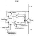
- FIG. 1 is a diagram showing one of switching circuits in a power converter and the flow of signals according to a first embodiment of the present invention.
- the switching circuit of the present embodiment includes a power line 21, a switching element 9 and an active gate circuit 11.
- a power line 21 is connected to the emitter terminal and the collector terminal of the switching element 9.
- the active gate circuit 11 is connected to the gate terminal of the switching element 9.
- the active gate circuit 11 includes voltage amplifiers 2 and 5, a gate resistor 3, and a control current source 6.
- the switching circuit also includes a voltage detector 4 and a delay device 12.
- the voltage detector 4 detects the emitter-side voltage of the switching element 9 and transmits a signal to the voltage amplifier 5.
- the delay device 12 receives a gate signal 14 and a delay-amount setting signal 15 and transmits an output signal to the voltage amplifier 2.
- the switching element 9 is a voltage-controlled switching element of non-latching type such as an IGBT or a MOSFET.
- the power converter of the present embodiment includes an arm for DC-to-AC conversion. The arm has a plurality of the switching circuits of the same structure shown in FIG. 1 connected in series.
- the delay device 12 delays transmitting the gate signal 14 to the voltage amplifier 2 according to the delay-amount setting signal 15.
- the gate signal 14 is transmitted to all the switching elements in common from a control unit that is located in a low-potential section of the power converter.
- a switching element has a smaller storage time, it takes a shorter time for the switching element to actually turn off after the gate signal 14 is switched off.
- the delay-amount setting signal 15 is thus set to be higher than that of the other switching elements in level so as to increase the delay amount (the amount of delay) of the delay device 12. This makes the turn-off timing coincident with those of the other switching elements so that the switching element bears the same amount of loss as the other switching elements do.
- the operation delay of a switching element occurs mostly on the turn-off side. This phenomenon is particularly noticeable in switching elements that make a bipolar operation like an IGBT. For such switching elements, it is desired that variations of the operation delay are adjusted only on the turn-off side and are not adjusted on the turn-on side.
- the delay device 12 is configured so as to operate only on the turn-off side. Alternatively, different delay devices are desirably used on the turn-on side and on the turn-off side.
- the power converter having a plurality of switching elements connected in series can thus suppress a surge voltage generated on the switching elements and prevent the concentration of loss on a particular switching element.
- a method of setting the delay-amount setting signal 15 of the first embodiment will be described.
- Possible methods for setting the delay-amount setting signal 15 are broadly classified into two.
- One of the methods is to conduct an interruption test and the like in a factory before shipment, and set the amounts of delay so as to absorb differences in the operation delay attributable to differences between the storage times of the respective switching elements.
- the other is to detect differences in the operation delay between the switching elements during operation and dynamically adjust the amounts of delay.
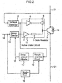
- the present embodiment is of the latter method. More specifically, as shown in FIG. 2 , the present embodiment includes a sample-and-hold circuit 16, a delay-amount adjuster 17, and a sampling control circuit 18 aside from the configuration shown in FIG. 1 .
- the output of the voltage detector 4 is transmitted to the sample-and-hold circuit 16.
- the delay-amount adjuster 17 transmits the delay-amount setting signal 15 that is adjusted according to the output of the sample-and-hold circuit 16.
- the delay device 12 accordingly delays transmitting the gate signal 14 for driving the switching element 9.
- the sample-and-hold circuit 16 is controlled by the sampling control circuit 18.
- the sample-and-hold circuit 16 performs a sampling operation in time with the reset of the held output and turn-off timing over a period as long as or longer than a single cycle of the output current of the power converter based on the gate signal 14.
- FIG. 3 shows the voltage and current waveforms of various parts of such a power converter.
- the output current of the power converter is a near sinusoidal wave.
- the current of the switching element 9 including the current of a flywheel diode (FWD) 10 which is connected in parallel has the shape of the output current notched by PWM switching.
- the collector-to-emitter voltage Vce of the switching element 9 is the same as the power supply voltage.
- the surge voltage immediately after turn-off generally tends to increase with the current that flows through the switching element 9.
- the peak value of the collector-to-emitter voltage Vce varies within a single cycle of the output current of the power converter.
- Such switching timing refers to when the switching element 9 interrupts the highest current in a single cycle.
- the collector-to-emitter voltage is detected by the voltage detector 4, and is sampled in synchronization with the turn-off timing of the gate signal 14 by the sample-and-hold circuit 16.
- the sampled value by the sample-and-hold circuit 16 is compared with the hold value outputted at the point in time. If the sampled value exceeds the hold value, the hold output is adjusted to the sampled value.
- Such a sample-and-hold operation is performed for a single cycle, so that the output of the sample-and-hold circuit 16 has a value equivalent to the maximum value of the collector-to-emitter voltage Vce.
- the delay amount of the gate signal 14 by the delay device 12 is adjusted so as to suppress the maximum value of the collector-to-emitter voltage in a period as long as or longer than a single cycle period of the power converter. That is, the operation compensates the delay of the switching element 9 with the delay device 12.
- the delay amount is adjusted according to the collector-to-emitter voltage Vce of the switching element 9.
- the switching circuit of the present embodiment includes a timer counter 19 and a digital-to-analog (DA) converter 20 instead of the sample-and-hold circuit 16 of the second embodiment ( FIG. 2 ).
- DA digital-to-analog
- the timer counter 19 monitors the input signal to the control current source 6, and counts the time span of operation of the active gate circuit 11.
- the DA converter 20 converts the count output into an analog signal.
- the delay-amount adjuster 17 converts the analog signal into the delay-amount setting signal 15, which determines the delay amount of the delay device 12.
- the sampling control circuit 18 controls the operation of the timer counter 19 and the DA converter 20 based on the gate signal 14.
- the active gate circuit 11 When the voltage of the switching element 9 exceeds a certain value, the active gate circuit 11 operates.
- the delay amount is set according to the operating time. Consequently, when the switching operation of the switching element 9 is faster than that of other elements, the delay amount is increased to suppress the difference in the operating time from the other elements so as to suppress an increase in loss.
- the delay amount may be increased in proportion to a value that is determined by subtracting a predetermined value from the peak value of the output of the voltage detector 4, or a value that is determined by subtracting a predetermined value from the operating time of the control current source 6.
- an extremely large delay amount may be set to cause a large element loss.
- a limiting means may be provided to limit the setting value of the delay amount within an allowable range.
- the present embodiment includes a comparing means for comparing the operating time of the control current source 6 between before and after the setting of the delay amount is changed.
- the comparing means can restore the setting before the change if the delay amount increased by a certain time makes the operating time too long. The operation of the comparing means will be described with reference to the flowchart of FIG. 5 .
- the operating time (operating time before a change) of the active gate circuit 11 is inputted to the delay-amount adjuster 17 (step S2).
- the delay amount increased by a certain time is outputted (steps S3 and S4).
- the operating time (operating time after the change) of the active gate circuit 11 is inputted to the delay-amount adjuster 17 again (step S6).
- the operating time before the change and the operating time after the change are compared with each other (step S7). If the operating time after the change is longer than the operating time before the change, the delay amount is restored to that before the change (step S8). If the operating time after the change is shorter than or equal to the operating time before the change, the delay amount after the change is maintained.
- the comparing means may compare the peak value of the output of the voltage detector 4 between before and after the change of the setting (step S7).
- the present embodiment deals with the delay-amount adjuster 17 according to the foregoing second or third embodiments ( FIGS. 2 , 4 ).
- the loss-based temperature increase of the switching element is dominated by the thermal time constant of the switching element.
- the thermal time constant is from several hundreds of milliseconds to several seconds, far longer than electric operations.
- the delay-amount adjuster 17 can make a simple integral operation of long time constant.
- the operation of the delay-amount adjuster 17 may otherwise be performed digitally. Such a digital operation will be described with reference to the flowchart of FIG. 6 .
- the operating time of the active gate circuit 11 is input to the delay-amount adjuster 17 (step S12).
- the operating time is compared with a predetermined threshold (step S13). If the threshold is exceeded and the delay amount is below a maximum value (step S14), the delay amount is increased by a certain time (step S15) and the resulting delay amount is output (step S16).
- step S17 After a lapse of time of a single cycle or more (step S17), the operating time of the active gate circuit 11 is input to the delay-amount adjuster 17 again (step S12). Consequently, if the active gate circuit 11 is operating for more than a certain duration, the delay amount is cyclically increased. The delay amount is then stabilized when the operating time of the active gate circuit 11 falls to or below the threshold.
- the delay time may be increased by unit time if the peak value of the output of the voltage detector 4 exceeds a predetermined value.
Landscapes
- Engineering & Computer Science (AREA)
- Power Engineering (AREA)
- Power Conversion In General (AREA)
- Inverter Devices (AREA)
- Dc-Dc Converters (AREA)
- Electronic Switches (AREA)
Applications Claiming Priority (2)
| Application Number | Priority Date | Filing Date | Title |
|---|---|---|---|
| JP2007276424 | 2007-10-24 | ||
| PCT/JP2008/003026 WO2009054143A1 (ja) | 2007-10-24 | 2008-10-24 | 電力変換装置 |
Publications (3)
| Publication Number | Publication Date |
|---|---|
| EP2204897A1 EP2204897A1 (en) | 2010-07-07 |
| EP2204897A4 EP2204897A4 (en) | 2017-04-05 |
| EP2204897B1 true EP2204897B1 (en) | 2019-11-27 |
Family
ID=40579251
Family Applications (1)
| Application Number | Title | Priority Date | Filing Date |
|---|---|---|---|
| EP08843267.9A Active EP2204897B1 (en) | 2007-10-24 | 2008-10-24 | Power converter |
Country Status (5)
| Country | Link |
|---|---|
| US (1) | US8836311B2 (ja) |
| EP (1) | EP2204897B1 (ja) |
| JP (1) | JPWO2009054143A1 (ja) |
| CN (1) | CN101836350B (ja) |
| WO (1) | WO2009054143A1 (ja) |
Families Citing this family (8)
| Publication number | Priority date | Publication date | Assignee | Title |
|---|---|---|---|---|
| US8611109B2 (en) * | 2010-09-30 | 2013-12-17 | Infineon Technologies Ag | Flyback converter with an adaptively controlled rectifier arrangement |
| DE112015006874T5 (de) * | 2015-09-03 | 2018-05-30 | Mitsubishi Electric Corporation | Leistungswandler |
| JP6602266B2 (ja) | 2016-06-06 | 2019-11-06 | 株式会社東芝 | 半導体装置、電力変換装置、及び、車両 |
| US10326373B1 (en) * | 2017-12-29 | 2019-06-18 | Texas Instruments Incorporated | Programmable switching converter |
| WO2020059262A1 (ja) * | 2018-09-19 | 2020-03-26 | パナソニックIpマネジメント株式会社 | 突入電流抑制装置及びモータ駆動装置 |
| JP7273629B2 (ja) * | 2019-06-25 | 2023-05-15 | 株式会社東芝 | 電力変換装置 |
| CN110994961B (zh) * | 2019-12-24 | 2020-11-20 | 浙江大学 | 功率开关管串联运行门极电压幅值补偿均压方法和电路 |
| JP2022043842A (ja) * | 2020-09-04 | 2022-03-16 | 株式会社東芝 | 電子回路及び電力変換器 |
Family Cites Families (14)
| Publication number | Priority date | Publication date | Assignee | Title |
|---|---|---|---|---|
| DE4335857A1 (de) * | 1993-10-21 | 1995-04-27 | Abb Management Ag | Stromrichterschaltungsanordnung und Verfahren zur Ansteuerung derselben |
| JP3254159B2 (ja) * | 1997-02-04 | 2002-02-04 | セイコーインスツルメンツ株式会社 | 充放電制御回路 |
| DE19838389C1 (de) * | 1998-08-24 | 2000-03-09 | Siemens Ag | Verfahren und Vorrichtung zur Steuerung eines abschaltbaren Stromrichterventils mit der Reihenschaltzahl Zwei oder größer |
| JP2000324799A (ja) * | 1999-05-10 | 2000-11-24 | Meidensha Corp | 半導体電力変換器 |
| JP2001231247A (ja) * | 2000-02-17 | 2001-08-24 | Fuji Electric Co Ltd | ゲート駆動方法 |
| JP3791400B2 (ja) * | 2001-11-22 | 2006-06-28 | 三菱電機株式会社 | 半導体装置 |
| JP3883925B2 (ja) * | 2002-07-30 | 2007-02-21 | 三菱電機株式会社 | 電力用半導体素子の駆動回路 |
| JP4230190B2 (ja) * | 2002-10-16 | 2009-02-25 | 東芝三菱電機産業システム株式会社 | 電力変換装置 |
| JP2004228768A (ja) * | 2003-01-21 | 2004-08-12 | Toshiba Corp | ゲート駆動回路 |
| JP4313088B2 (ja) * | 2003-05-22 | 2009-08-12 | 三菱電機株式会社 | 半導体装置 |
| JP3799341B2 (ja) * | 2003-07-25 | 2006-07-19 | 株式会社東芝 | ゲート駆動回路及び半導体装置 |
| JP4342251B2 (ja) * | 2003-09-10 | 2009-10-14 | 株式会社東芝 | ゲート駆動回路 |
| JP4874665B2 (ja) * | 2006-02-14 | 2012-02-15 | 株式会社東芝 | ゲート駆動回路 |
| JP4710749B2 (ja) * | 2006-07-28 | 2011-06-29 | 富士電機システムズ株式会社 | Dc−dcコンバータの制御回路及び方法 |
-
2008
- 2008-10-24 WO PCT/JP2008/003026 patent/WO2009054143A1/ja active Application Filing
- 2008-10-24 JP JP2009537944A patent/JPWO2009054143A1/ja not_active Withdrawn
- 2008-10-24 EP EP08843267.9A patent/EP2204897B1/en active Active
- 2008-10-24 CN CN2008801125488A patent/CN101836350B/zh active Active
-
2010
- 2010-04-09 US US12/757,491 patent/US8836311B2/en active Active
Non-Patent Citations (1)
| Title |
|---|
| None * |
Also Published As
| Publication number | Publication date |
|---|---|
| US20100219877A1 (en) | 2010-09-02 |
| WO2009054143A1 (ja) | 2009-04-30 |
| EP2204897A1 (en) | 2010-07-07 |
| US8836311B2 (en) | 2014-09-16 |
| CN101836350B (zh) | 2013-02-06 |
| CN101836350A (zh) | 2010-09-15 |
| EP2204897A4 (en) | 2017-04-05 |
| JPWO2009054143A1 (ja) | 2011-03-03 |
Similar Documents
| Publication | Publication Date | Title |
|---|---|---|
| EP2204897B1 (en) | Power converter | |
| KR100353293B1 (ko) | 직렬회로반도체스위치의구동방법및회로장치 | |
| US20120230076A1 (en) | Voltage balancing | |
| EP3447918B1 (en) | Multi-stage gate turn-off with dynamic timing | |
| US8994413B2 (en) | Method for driving power semiconductor switches | |
| EP2424112B1 (en) | Current balancing of parallel connected semiconductor components | |
| JP6171553B2 (ja) | 電力変換装置 | |
| US8363440B2 (en) | Power conversion circuit having off-voltage control circuit | |
| US10230354B2 (en) | Voltage balancing in series-connected power switches | |
| EP2816728A1 (en) | Active gate drive circuit | |
| JP2004229382A (ja) | ゲート駆動回路、および電力変換装置 | |
| EP2586126B1 (en) | Voltage converting apparatus and method for converting a voltage | |
| JP2008017558A (ja) | スイッチング素子駆動回路 | |
| US20030095365A1 (en) | Semiconductor equipment | |
| JP2008048569A (ja) | 半導体スイッチング素子の駆動回路および電力変換装置 | |
| JP3772534B2 (ja) | 半導体電力変換器 | |
| JP4061741B2 (ja) | 半導体スイッチのスイッチング信号調整装置 | |
| JP4313088B2 (ja) | 半導体装置 | |
| CN110192344B (zh) | 用于驱控双极可开关功率半导体器件的控制装置、半导体模块和方法 | |
| JPH10322881A (ja) | 直列に接続されたターン・オフ型の電力用半導体デバイスに対する短絡回路現象の検出および処理のための方法とデバイス | |
| JP7171946B1 (ja) | 電源装置 | |
| EP3955464A1 (en) | Drive circuit of power semiconductor element | |
| Li et al. | Less Losses with Less Oscillations–How to Achieve This at SiC MOSFET Turn-On across the Full Operating Range | |
| US20240128966A1 (en) | Drive circuit for semiconductor switching device | |
| CN110291719B (zh) | 驱控功率半导体器件的控制装置和驱控功率半导体器件的方法 |
Legal Events
| Date | Code | Title | Description |
|---|---|---|---|
| PUAI | Public reference made under article 153(3) epc to a published international application that has entered the european phase |
Free format text: ORIGINAL CODE: 0009012 |
|
| 17P | Request for examination filed |
Effective date: 20100422 |
|
| AK | Designated contracting states |
Kind code of ref document: A1 Designated state(s): AT BE BG CH CY CZ DE DK EE ES FI FR GB GR HR HU IE IS IT LI LT LU LV MC MT NL NO PL PT RO SE SI SK TR |
|
| AX | Request for extension of the european patent |
Extension state: AL BA MK RS |
|
| DAX | Request for extension of the european patent (deleted) | ||
| RA4 | Supplementary search report drawn up and despatched (corrected) |
Effective date: 20170307 |
|
| RIC1 | Information provided on ipc code assigned before grant |
Ipc: H02M 1/088 20060101ALI20170301BHEP Ipc: H03K 17/16 20060101ALI20170301BHEP Ipc: H02M 1/00 20070101ALI20170301BHEP Ipc: H02M 1/08 20060101AFI20170301BHEP Ipc: H03K 17/28 20060101ALI20170301BHEP |
|
| GRAP | Despatch of communication of intention to grant a patent |
Free format text: ORIGINAL CODE: EPIDOSNIGR1 |
|
| STAA | Information on the status of an ep patent application or granted ep patent |
Free format text: STATUS: GRANT OF PATENT IS INTENDED |
|
| INTG | Intention to grant announced |
Effective date: 20190516 |
|
| GRAJ | Information related to disapproval of communication of intention to grant by the applicant or resumption of examination proceedings by the epo deleted |
Free format text: ORIGINAL CODE: EPIDOSDIGR1 |
|
| STAA | Information on the status of an ep patent application or granted ep patent |
Free format text: STATUS: REQUEST FOR EXAMINATION WAS MADE |
|
| GRAP | Despatch of communication of intention to grant a patent |
Free format text: ORIGINAL CODE: EPIDOSNIGR1 |
|
| STAA | Information on the status of an ep patent application or granted ep patent |
Free format text: STATUS: GRANT OF PATENT IS INTENDED |
|
| INTC | Intention to grant announced (deleted) | ||
| INTG | Intention to grant announced |
Effective date: 20190731 |
|
| GRAS | Grant fee paid |
Free format text: ORIGINAL CODE: EPIDOSNIGR3 |
|
| GRAA | (expected) grant |
Free format text: ORIGINAL CODE: 0009210 |
|
| STAA | Information on the status of an ep patent application or granted ep patent |
Free format text: STATUS: THE PATENT HAS BEEN GRANTED |
|
| AK | Designated contracting states |
Kind code of ref document: B1 Designated state(s): AT BE BG CH CY CZ DE DK EE ES FI FR GB GR HR HU IE IS IT LI LT LU LV MC MT NL NO PL PT RO SE SI SK TR |
|
| REG | Reference to a national code |
Ref country code: GB Ref legal event code: FG4D |
|
| REG | Reference to a national code |
Ref country code: CH Ref legal event code: EP |
|
| REG | Reference to a national code |
Ref country code: AT Ref legal event code: REF Ref document number: 1207850 Country of ref document: AT Kind code of ref document: T Effective date: 20191215 |
|
| REG | Reference to a national code |
Ref country code: DE Ref legal event code: R096 Ref document number: 602008061726 Country of ref document: DE |
|
| REG | Reference to a national code |
Ref country code: IE Ref legal event code: FG4D |
|
| REG | Reference to a national code |
Ref country code: NL Ref legal event code: MP Effective date: 20191127 |
|
| REG | Reference to a national code |
Ref country code: LT Ref legal event code: MG4D |
|
| PG25 | Lapsed in a contracting state [announced via postgrant information from national office to epo] |
Ref country code: ES Free format text: LAPSE BECAUSE OF FAILURE TO SUBMIT A TRANSLATION OF THE DESCRIPTION OR TO PAY THE FEE WITHIN THE PRESCRIBED TIME-LIMIT Effective date: 20191127 Ref country code: NL Free format text: LAPSE BECAUSE OF FAILURE TO SUBMIT A TRANSLATION OF THE DESCRIPTION OR TO PAY THE FEE WITHIN THE PRESCRIBED TIME-LIMIT Effective date: 20191127 Ref country code: LT Free format text: LAPSE BECAUSE OF FAILURE TO SUBMIT A TRANSLATION OF THE DESCRIPTION OR TO PAY THE FEE WITHIN THE PRESCRIBED TIME-LIMIT Effective date: 20191127 Ref country code: GR Free format text: LAPSE BECAUSE OF FAILURE TO SUBMIT A TRANSLATION OF THE DESCRIPTION OR TO PAY THE FEE WITHIN THE PRESCRIBED TIME-LIMIT Effective date: 20200228 Ref country code: NO Free format text: LAPSE BECAUSE OF FAILURE TO SUBMIT A TRANSLATION OF THE DESCRIPTION OR TO PAY THE FEE WITHIN THE PRESCRIBED TIME-LIMIT Effective date: 20200227 Ref country code: FI Free format text: LAPSE BECAUSE OF FAILURE TO SUBMIT A TRANSLATION OF THE DESCRIPTION OR TO PAY THE FEE WITHIN THE PRESCRIBED TIME-LIMIT Effective date: 20191127 Ref country code: LV Free format text: LAPSE BECAUSE OF FAILURE TO SUBMIT A TRANSLATION OF THE DESCRIPTION OR TO PAY THE FEE WITHIN THE PRESCRIBED TIME-LIMIT Effective date: 20191127 Ref country code: SE Free format text: LAPSE BECAUSE OF FAILURE TO SUBMIT A TRANSLATION OF THE DESCRIPTION OR TO PAY THE FEE WITHIN THE PRESCRIBED TIME-LIMIT Effective date: 20191127 Ref country code: BG Free format text: LAPSE BECAUSE OF FAILURE TO SUBMIT A TRANSLATION OF THE DESCRIPTION OR TO PAY THE FEE WITHIN THE PRESCRIBED TIME-LIMIT Effective date: 20200227 |
|
| PG25 | Lapsed in a contracting state [announced via postgrant information from national office to epo] |
Ref country code: IS Free format text: LAPSE BECAUSE OF FAILURE TO SUBMIT A TRANSLATION OF THE DESCRIPTION OR TO PAY THE FEE WITHIN THE PRESCRIBED TIME-LIMIT Effective date: 20200327 Ref country code: HR Free format text: LAPSE BECAUSE OF FAILURE TO SUBMIT A TRANSLATION OF THE DESCRIPTION OR TO PAY THE FEE WITHIN THE PRESCRIBED TIME-LIMIT Effective date: 20191127 |
|
| PG25 | Lapsed in a contracting state [announced via postgrant information from national office to epo] |
Ref country code: PT Free format text: LAPSE BECAUSE OF FAILURE TO SUBMIT A TRANSLATION OF THE DESCRIPTION OR TO PAY THE FEE WITHIN THE PRESCRIBED TIME-LIMIT Effective date: 20200419 Ref country code: EE Free format text: LAPSE BECAUSE OF FAILURE TO SUBMIT A TRANSLATION OF THE DESCRIPTION OR TO PAY THE FEE WITHIN THE PRESCRIBED TIME-LIMIT Effective date: 20191127 Ref country code: DK Free format text: LAPSE BECAUSE OF FAILURE TO SUBMIT A TRANSLATION OF THE DESCRIPTION OR TO PAY THE FEE WITHIN THE PRESCRIBED TIME-LIMIT Effective date: 20191127 Ref country code: RO Free format text: LAPSE BECAUSE OF FAILURE TO SUBMIT A TRANSLATION OF THE DESCRIPTION OR TO PAY THE FEE WITHIN THE PRESCRIBED TIME-LIMIT Effective date: 20191127 Ref country code: CZ Free format text: LAPSE BECAUSE OF FAILURE TO SUBMIT A TRANSLATION OF THE DESCRIPTION OR TO PAY THE FEE WITHIN THE PRESCRIBED TIME-LIMIT Effective date: 20191127 |
|
| REG | Reference to a national code |
Ref country code: DE Ref legal event code: R097 Ref document number: 602008061726 Country of ref document: DE |
|
| PG25 | Lapsed in a contracting state [announced via postgrant information from national office to epo] |
Ref country code: SK Free format text: LAPSE BECAUSE OF FAILURE TO SUBMIT A TRANSLATION OF THE DESCRIPTION OR TO PAY THE FEE WITHIN THE PRESCRIBED TIME-LIMIT Effective date: 20191127 |
|
| REG | Reference to a national code |
Ref country code: AT Ref legal event code: MK05 Ref document number: 1207850 Country of ref document: AT Kind code of ref document: T Effective date: 20191127 |
|
| PLBE | No opposition filed within time limit |
Free format text: ORIGINAL CODE: 0009261 |
|
| STAA | Information on the status of an ep patent application or granted ep patent |
Free format text: STATUS: NO OPPOSITION FILED WITHIN TIME LIMIT |
|
| 26N | No opposition filed |
Effective date: 20200828 |
|
| PG25 | Lapsed in a contracting state [announced via postgrant information from national office to epo] |
Ref country code: SI Free format text: LAPSE BECAUSE OF FAILURE TO SUBMIT A TRANSLATION OF THE DESCRIPTION OR TO PAY THE FEE WITHIN THE PRESCRIBED TIME-LIMIT Effective date: 20191127 Ref country code: PL Free format text: LAPSE BECAUSE OF FAILURE TO SUBMIT A TRANSLATION OF THE DESCRIPTION OR TO PAY THE FEE WITHIN THE PRESCRIBED TIME-LIMIT Effective date: 20191127 Ref country code: AT Free format text: LAPSE BECAUSE OF FAILURE TO SUBMIT A TRANSLATION OF THE DESCRIPTION OR TO PAY THE FEE WITHIN THE PRESCRIBED TIME-LIMIT Effective date: 20191127 |
|
| PG25 | Lapsed in a contracting state [announced via postgrant information from national office to epo] |
Ref country code: IT Free format text: LAPSE BECAUSE OF FAILURE TO SUBMIT A TRANSLATION OF THE DESCRIPTION OR TO PAY THE FEE WITHIN THE PRESCRIBED TIME-LIMIT Effective date: 20191127 |
|
| REG | Reference to a national code |
Ref country code: CH Ref legal event code: PL |
|
| GBPC | Gb: european patent ceased through non-payment of renewal fee |
Effective date: 20201024 |
|
| PG25 | Lapsed in a contracting state [announced via postgrant information from national office to epo] |
Ref country code: MC Free format text: LAPSE BECAUSE OF FAILURE TO SUBMIT A TRANSLATION OF THE DESCRIPTION OR TO PAY THE FEE WITHIN THE PRESCRIBED TIME-LIMIT Effective date: 20191127 Ref country code: LU Free format text: LAPSE BECAUSE OF NON-PAYMENT OF DUE FEES Effective date: 20201024 |
|
| REG | Reference to a national code |
Ref country code: BE Ref legal event code: MM Effective date: 20201031 |
|
| PG25 | Lapsed in a contracting state [announced via postgrant information from national office to epo] |
Ref country code: FR Free format text: LAPSE BECAUSE OF NON-PAYMENT OF DUE FEES Effective date: 20201031 |
|
| PG25 | Lapsed in a contracting state [announced via postgrant information from national office to epo] |
Ref country code: LI Free format text: LAPSE BECAUSE OF NON-PAYMENT OF DUE FEES Effective date: 20201031 Ref country code: GB Free format text: LAPSE BECAUSE OF NON-PAYMENT OF DUE FEES Effective date: 20201024 Ref country code: CH Free format text: LAPSE BECAUSE OF NON-PAYMENT OF DUE FEES Effective date: 20201031 Ref country code: BE Free format text: LAPSE BECAUSE OF NON-PAYMENT OF DUE FEES Effective date: 20201031 |
|
| PG25 | Lapsed in a contracting state [announced via postgrant information from national office to epo] |
Ref country code: IE Free format text: LAPSE BECAUSE OF NON-PAYMENT OF DUE FEES Effective date: 20201024 |
|
| PG25 | Lapsed in a contracting state [announced via postgrant information from national office to epo] |
Ref country code: TR Free format text: LAPSE BECAUSE OF FAILURE TO SUBMIT A TRANSLATION OF THE DESCRIPTION OR TO PAY THE FEE WITHIN THE PRESCRIBED TIME-LIMIT Effective date: 20191127 Ref country code: MT Free format text: LAPSE BECAUSE OF FAILURE TO SUBMIT A TRANSLATION OF THE DESCRIPTION OR TO PAY THE FEE WITHIN THE PRESCRIBED TIME-LIMIT Effective date: 20191127 Ref country code: CY Free format text: LAPSE BECAUSE OF FAILURE TO SUBMIT A TRANSLATION OF THE DESCRIPTION OR TO PAY THE FEE WITHIN THE PRESCRIBED TIME-LIMIT Effective date: 20191127 |
|
| PGFP | Annual fee paid to national office [announced via postgrant information from national office to epo] |
Ref country code: DE Payment date: 20230830 Year of fee payment: 16 |