EP2200838B1 - Procédé pour fournir une couche de métal dessinée ayant une conductivité élevée - Google Patents
Procédé pour fournir une couche de métal dessinée ayant une conductivité élevée Download PDFInfo
- Publication number
- EP2200838B1 EP2200838B1 EP08842620A EP08842620A EP2200838B1 EP 2200838 B1 EP2200838 B1 EP 2200838B1 EP 08842620 A EP08842620 A EP 08842620A EP 08842620 A EP08842620 A EP 08842620A EP 2200838 B1 EP2200838 B1 EP 2200838B1
- Authority
- EP
- European Patent Office
- Prior art keywords
- layer
- catalyst
- patterned
- metal
- fraction
- Prior art date
- Legal status (The legal status is an assumption and is not a legal conclusion. Google has not performed a legal analysis and makes no representation as to the accuracy of the status listed.)
- Not-in-force
Links
- 229910052751 metal Inorganic materials 0.000 title claims abstract description 119
- 239000002184 metal Substances 0.000 title claims abstract description 119
- 238000000034 method Methods 0.000 title claims abstract description 108
- 239000003054 catalyst Substances 0.000 claims abstract description 175
- 239000000758 substrate Substances 0.000 claims abstract description 98
- 238000007747 plating Methods 0.000 claims abstract description 38
- 238000001931 thermography Methods 0.000 claims abstract description 38
- 238000012546 transfer Methods 0.000 claims description 135
- 239000002318 adhesion promoter Substances 0.000 claims description 77
- 239000011521 glass Substances 0.000 claims description 64
- 230000003667 anti-reflective effect Effects 0.000 claims description 31
- 239000000463 material Substances 0.000 claims description 28
- 229920005596 polymer binder Polymers 0.000 claims description 26
- 239000002491 polymer binding agent Substances 0.000 claims description 26
- -1 silicate hydroxides Chemical class 0.000 claims description 26
- 239000000975 dye Substances 0.000 claims description 23
- 229910052802 copper Inorganic materials 0.000 claims description 22
- 229920005862 polyol Polymers 0.000 claims description 22
- 150000004703 alkoxides Chemical class 0.000 claims description 20
- 150000003077 polyols Chemical class 0.000 claims description 20
- 238000010438 heat treatment Methods 0.000 claims description 17
- 229910052759 nickel Inorganic materials 0.000 claims description 16
- 229910000000 metal hydroxide Inorganic materials 0.000 claims description 15
- 150000004692 metal hydroxides Chemical class 0.000 claims description 15
- 229910052709 silver Inorganic materials 0.000 claims description 15
- 239000006100 radiation absorber Substances 0.000 claims description 14
- 229910045601 alloy Inorganic materials 0.000 claims description 13
- 239000000956 alloy Substances 0.000 claims description 13
- OKTJSMMVPCPJKN-UHFFFAOYSA-N Carbon Chemical compound [C] OKTJSMMVPCPJKN-UHFFFAOYSA-N 0.000 claims description 12
- 239000000843 powder Substances 0.000 claims description 12
- 150000004706 metal oxides Chemical class 0.000 claims description 10
- 239000002923 metal particle Substances 0.000 claims description 10
- 229910052804 chromium Inorganic materials 0.000 claims description 9
- 229910044991 metal oxide Inorganic materials 0.000 claims description 9
- 239000006229 carbon black Substances 0.000 claims description 8
- 150000003839 salts Chemical class 0.000 claims description 8
- 229910052799 carbon Inorganic materials 0.000 claims description 6
- 229910052742 iron Inorganic materials 0.000 claims description 6
- 238000010521 absorption reaction Methods 0.000 claims description 5
- 229910052782 aluminium Inorganic materials 0.000 claims description 5
- 239000010439 graphite Substances 0.000 claims description 5
- 229910002804 graphite Inorganic materials 0.000 claims description 5
- 229910052763 palladium Inorganic materials 0.000 claims description 5
- 229910052718 tin Inorganic materials 0.000 claims description 5
- 229910052707 ruthenium Inorganic materials 0.000 claims description 4
- 239000000919 ceramic Substances 0.000 claims description 3
- 230000001404 mediated effect Effects 0.000 claims description 3
- 229910052697 platinum Inorganic materials 0.000 claims description 3
- 229910052737 gold Inorganic materials 0.000 claims description 2
- 229910052741 iridium Inorganic materials 0.000 claims description 2
- 239000000615 nonconductor Substances 0.000 claims description 2
- 229910052762 osmium Inorganic materials 0.000 claims description 2
- 229910052703 rhodium Inorganic materials 0.000 claims description 2
- 239000010410 layer Substances 0.000 description 324
- 239000002585 base Substances 0.000 description 69
- 239000010408 film Substances 0.000 description 66
- 239000010949 copper Substances 0.000 description 49
- 238000003384 imaging method Methods 0.000 description 39
- 229920001577 copolymer Polymers 0.000 description 38
- 239000000523 sample Substances 0.000 description 32
- 239000003795 chemical substances by application Substances 0.000 description 29
- 125000000217 alkyl group Chemical group 0.000 description 27
- PXHVJJICTQNCMI-UHFFFAOYSA-N Nickel Chemical compound [Ni] PXHVJJICTQNCMI-UHFFFAOYSA-N 0.000 description 23
- 238000000576 coating method Methods 0.000 description 23
- PPBRXRYQALVLMV-UHFFFAOYSA-N Styrene Chemical compound C=CC1=CC=CC=C1 PPBRXRYQALVLMV-UHFFFAOYSA-N 0.000 description 21
- NIXOWILDQLNWCW-UHFFFAOYSA-N acrylic acid group Chemical group C(C=C)(=O)O NIXOWILDQLNWCW-UHFFFAOYSA-N 0.000 description 21
- 238000009713 electroplating Methods 0.000 description 21
- 239000011248 coating agent Substances 0.000 description 20
- 239000000243 solution Substances 0.000 description 20
- 229920000642 polymer Polymers 0.000 description 19
- 239000011230 binding agent Substances 0.000 description 18
- 239000004615 ingredient Substances 0.000 description 17
- 239000000203 mixture Substances 0.000 description 17
- 229920000728 polyester Polymers 0.000 description 14
- 230000005855 radiation Effects 0.000 description 14
- 229920000058 polyacrylate Polymers 0.000 description 13
- 238000003756 stirring Methods 0.000 description 13
- WOCIAKWEIIZHES-UHFFFAOYSA-N ruthenium(iv) oxide Chemical compound O=[Ru]=O WOCIAKWEIIZHES-UHFFFAOYSA-N 0.000 description 12
- NIXOWILDQLNWCW-UHFFFAOYSA-M Acrylate Chemical compound [O-]C(=O)C=C NIXOWILDQLNWCW-UHFFFAOYSA-M 0.000 description 11
- RYGMFSIKBFXOCR-UHFFFAOYSA-N Copper Chemical compound [Cu] RYGMFSIKBFXOCR-UHFFFAOYSA-N 0.000 description 11
- 239000011651 chromium Substances 0.000 description 11
- 239000002245 particle Substances 0.000 description 11
- XLYOFNOQVPJJNP-UHFFFAOYSA-N water Chemical compound O XLYOFNOQVPJJNP-UHFFFAOYSA-N 0.000 description 11
- 238000000151 deposition Methods 0.000 description 10
- CERQOIWHTDAKMF-UHFFFAOYSA-N Methacrylic acid Chemical compound CC(=C)C(O)=O CERQOIWHTDAKMF-UHFFFAOYSA-N 0.000 description 9
- XTXRWKRVRITETP-UHFFFAOYSA-N Vinyl acetate Chemical compound CC(=O)OC=C XTXRWKRVRITETP-UHFFFAOYSA-N 0.000 description 9
- 150000002739 metals Chemical class 0.000 description 9
- 238000000527 sonication Methods 0.000 description 9
- XLOMVQKBTHCTTD-UHFFFAOYSA-N Zinc monoxide Chemical compound [Zn]=O XLOMVQKBTHCTTD-UHFFFAOYSA-N 0.000 description 8
- 239000002253 acid Substances 0.000 description 8
- 238000004519 manufacturing process Methods 0.000 description 8
- 239000000178 monomer Substances 0.000 description 8
- 239000007864 aqueous solution Substances 0.000 description 7
- 230000015572 biosynthetic process Effects 0.000 description 7
- 238000007772 electroless plating Methods 0.000 description 7
- 229910052739 hydrogen Inorganic materials 0.000 description 7
- 239000001257 hydrogen Substances 0.000 description 7
- XEEYBQQBJWHFJM-UHFFFAOYSA-N iron Substances [Fe] XEEYBQQBJWHFJM-UHFFFAOYSA-N 0.000 description 7
- KDLHZDBZIXYQEI-UHFFFAOYSA-N palladium Substances [Pd] KDLHZDBZIXYQEI-UHFFFAOYSA-N 0.000 description 7
- 239000010944 silver (metal) Substances 0.000 description 7
- 229920000178 Acrylic resin Polymers 0.000 description 6
- 239000004925 Acrylic resin Substances 0.000 description 6
- VYZAMTAEIAYCRO-UHFFFAOYSA-N Chromium Chemical compound [Cr] VYZAMTAEIAYCRO-UHFFFAOYSA-N 0.000 description 6
- KWYUFKZDYYNOTN-UHFFFAOYSA-M Potassium hydroxide Chemical compound [OH-].[K+] KWYUFKZDYYNOTN-UHFFFAOYSA-M 0.000 description 6
- JUJWROOIHBZHMG-UHFFFAOYSA-N Pyridine Chemical compound C1=CC=NC=C1 JUJWROOIHBZHMG-UHFFFAOYSA-N 0.000 description 6
- 239000000853 adhesive Substances 0.000 description 6
- 230000001070 adhesive effect Effects 0.000 description 6
- 235000019241 carbon black Nutrition 0.000 description 6
- 239000006185 dispersion Substances 0.000 description 6
- FPYJFEHAWHCUMM-UHFFFAOYSA-N maleic anhydride Chemical compound O=C1OC(=O)C=C1 FPYJFEHAWHCUMM-UHFFFAOYSA-N 0.000 description 6
- 229920000139 polyethylene terephthalate Polymers 0.000 description 6
- 239000005020 polyethylene terephthalate Substances 0.000 description 6
- 229920002689 polyvinyl acetate Polymers 0.000 description 6
- UGFAIRIUMAVXCW-UHFFFAOYSA-N Carbon monoxide Chemical compound [O+]#[C-] UGFAIRIUMAVXCW-UHFFFAOYSA-N 0.000 description 5
- VGGSQFUCUMXWEO-UHFFFAOYSA-N Ethene Chemical compound C=C VGGSQFUCUMXWEO-UHFFFAOYSA-N 0.000 description 5
- 239000005977 Ethylene Substances 0.000 description 5
- 239000004721 Polyphenylene oxide Substances 0.000 description 5
- 229910002091 carbon monoxide Inorganic materials 0.000 description 5
- 238000001035 drying Methods 0.000 description 5
- 239000012530 fluid Substances 0.000 description 5
- 125000002887 hydroxy group Chemical group [H]O* 0.000 description 5
- WXZMFSXDPGVJKK-UHFFFAOYSA-N pentaerythritol Chemical compound OCC(CO)(CO)CO WXZMFSXDPGVJKK-UHFFFAOYSA-N 0.000 description 5
- 229920000570 polyether Polymers 0.000 description 5
- 239000011118 polyvinyl acetate Substances 0.000 description 5
- 238000012545 processing Methods 0.000 description 5
- 238000011160 research Methods 0.000 description 5
- 229910052719 titanium Inorganic materials 0.000 description 5
- 239000010936 titanium Substances 0.000 description 5
- 239000011787 zinc oxide Substances 0.000 description 5
- CBECDWUDYQOTSW-UHFFFAOYSA-N 2-ethylbut-3-enal Chemical compound CCC(C=C)C=O CBECDWUDYQOTSW-UHFFFAOYSA-N 0.000 description 4
- IMROMDMJAWUWLK-UHFFFAOYSA-N Ethenol Chemical compound OC=C IMROMDMJAWUWLK-UHFFFAOYSA-N 0.000 description 4
- WHNWPMSKXPGLAX-UHFFFAOYSA-N N-Vinyl-2-pyrrolidone Chemical compound C=CN1CCCC1=O WHNWPMSKXPGLAX-UHFFFAOYSA-N 0.000 description 4
- BQCADISMDOOEFD-UHFFFAOYSA-N Silver Chemical compound [Ag] BQCADISMDOOEFD-UHFFFAOYSA-N 0.000 description 4
- BZHJMEDXRYGGRV-UHFFFAOYSA-N Vinyl chloride Chemical compound ClC=C BZHJMEDXRYGGRV-UHFFFAOYSA-N 0.000 description 4
- 239000012790 adhesive layer Substances 0.000 description 4
- 125000003710 aryl alkyl group Chemical group 0.000 description 4
- 125000004432 carbon atom Chemical group C* 0.000 description 4
- 238000006243 chemical reaction Methods 0.000 description 4
- 150000001875 compounds Chemical class 0.000 description 4
- 238000001914 filtration Methods 0.000 description 4
- 229920001519 homopolymer Polymers 0.000 description 4
- 239000000976 ink Substances 0.000 description 4
- 229910052748 manganese Inorganic materials 0.000 description 4
- 239000011572 manganese Substances 0.000 description 4
- 229910021645 metal ion Inorganic materials 0.000 description 4
- 238000002156 mixing Methods 0.000 description 4
- JFNLZVQOOSMTJK-KNVOCYPGSA-N norbornene Chemical compound C1[C@@H]2CC[C@H]1C=C2 JFNLZVQOOSMTJK-KNVOCYPGSA-N 0.000 description 4
- 239000000049 pigment Substances 0.000 description 4
- 239000004332 silver Substances 0.000 description 4
- 239000002904 solvent Substances 0.000 description 4
- 239000000126 substance Substances 0.000 description 4
- 239000011135 tin Substances 0.000 description 4
- 229920006163 vinyl copolymer Polymers 0.000 description 4
- 229920002554 vinyl polymer Polymers 0.000 description 4
- 239000008096 xylene Substances 0.000 description 4
- 229910052725 zinc Inorganic materials 0.000 description 4
- 239000011701 zinc Substances 0.000 description 4
- 229910052726 zirconium Inorganic materials 0.000 description 4
- KTEFLEFPDDQMCB-UHFFFAOYSA-N 1,4-bis(4-butylanilino)-5,8-dihydroxyanthracene-9,10-dione Chemical compound C1=CC(CCCC)=CC=C1NC(C=1C(=O)C2=C(O)C=CC(O)=C2C(=O)C=11)=CC=C1NC1=CC=C(CCCC)C=C1 KTEFLEFPDDQMCB-UHFFFAOYSA-N 0.000 description 3
- LYCAIKOWRPUZTN-UHFFFAOYSA-N Ethylene glycol Chemical compound OCCO LYCAIKOWRPUZTN-UHFFFAOYSA-N 0.000 description 3
- IAYPIBMASNFSPL-UHFFFAOYSA-N Ethylene oxide Chemical compound C1CO1 IAYPIBMASNFSPL-UHFFFAOYSA-N 0.000 description 3
- PEDCQBHIVMGVHV-UHFFFAOYSA-N Glycerine Chemical compound OCC(O)CO PEDCQBHIVMGVHV-UHFFFAOYSA-N 0.000 description 3
- 229920005692 JONCRYL® Polymers 0.000 description 3
- 229910020615 PbO—SiO2 Inorganic materials 0.000 description 3
- HEMHJVSKTPXQMS-UHFFFAOYSA-M Sodium hydroxide Chemical compound [OH-].[Na+] HEMHJVSKTPXQMS-UHFFFAOYSA-M 0.000 description 3
- RTAQQCXQSZGOHL-UHFFFAOYSA-N Titanium Chemical compound [Ti] RTAQQCXQSZGOHL-UHFFFAOYSA-N 0.000 description 3
- ZJCCRDAZUWHFQH-UHFFFAOYSA-N Trimethylolpropane Chemical compound CCC(CO)(CO)CO ZJCCRDAZUWHFQH-UHFFFAOYSA-N 0.000 description 3
- 239000006096 absorbing agent Substances 0.000 description 3
- 239000011358 absorbing material Substances 0.000 description 3
- 238000000137 annealing Methods 0.000 description 3
- WERYXYBDKMZEQL-UHFFFAOYSA-N butane-1,4-diol Chemical compound OCCCCO WERYXYBDKMZEQL-UHFFFAOYSA-N 0.000 description 3
- 239000000084 colloidal system Substances 0.000 description 3
- 238000007796 conventional method Methods 0.000 description 3
- 230000008021 deposition Effects 0.000 description 3
- 125000005678 ethenylene group Chemical class [H]C([*:1])=C([H])[*:2] 0.000 description 3
- 239000000835 fiber Substances 0.000 description 3
- 238000009472 formulation Methods 0.000 description 3
- 150000002431 hydrogen Chemical class 0.000 description 3
- 125000004435 hydrogen atom Chemical group [H]* 0.000 description 3
- 229920002521 macromolecule Polymers 0.000 description 3
- BASFCYQUMIYNBI-UHFFFAOYSA-N platinum Substances [Pt] BASFCYQUMIYNBI-UHFFFAOYSA-N 0.000 description 3
- 229920000767 polyaniline Polymers 0.000 description 3
- 229920001296 polysiloxane Polymers 0.000 description 3
- 229920000123 polythiophene Polymers 0.000 description 3
- 230000001681 protective effect Effects 0.000 description 3
- UMJSCPRVCHMLSP-UHFFFAOYSA-N pyridine Natural products COC1=CC=CN=C1 UMJSCPRVCHMLSP-UHFFFAOYSA-N 0.000 description 3
- 239000012713 reactive precursor Substances 0.000 description 3
- 238000002310 reflectometry Methods 0.000 description 3
- 238000000926 separation method Methods 0.000 description 3
- VYPSYNLAJGMNEJ-UHFFFAOYSA-N silicon dioxide Inorganic materials O=[Si]=O VYPSYNLAJGMNEJ-UHFFFAOYSA-N 0.000 description 3
- 238000001228 spectrum Methods 0.000 description 3
- 229920001909 styrene-acrylic polymer Polymers 0.000 description 3
- 239000004094 surface-active agent Substances 0.000 description 3
- 229910052721 tungsten Inorganic materials 0.000 description 3
- 150000003738 xylenes Chemical class 0.000 description 3
- BHDWMMMNNQFZQJ-UHFFFAOYSA-M (2z)-2-[(2z)-2-[2-chloro-3-[(e)-2-(1,3,3-trimethylindol-1-ium-2-yl)ethenyl]cyclopent-2-en-1-ylidene]ethylidene]-1,3,3-trimethylindole;trifluoromethanesulfonate Chemical compound [O-]S(=O)(=O)C(F)(F)F.CC1(C)C2=CC=CC=C2N(C)\C1=C\C=C/1C(Cl)=C(\C=C\C=2C(C3=CC=CC=C3[N+]=2C)(C)C)CC\1 BHDWMMMNNQFZQJ-UHFFFAOYSA-M 0.000 description 2
- ZORQXIQZAOLNGE-UHFFFAOYSA-N 1,1-difluorocyclohexane Chemical compound FC1(F)CCCCC1 ZORQXIQZAOLNGE-UHFFFAOYSA-N 0.000 description 2
- SMZOUWXMTYCWNB-UHFFFAOYSA-N 2-(2-methoxy-5-methylphenyl)ethanamine Chemical compound COC1=CC=C(C)C=C1CCN SMZOUWXMTYCWNB-UHFFFAOYSA-N 0.000 description 2
- WMYINDVYGQKYMI-UHFFFAOYSA-N 2-[2,2-bis(hydroxymethyl)butoxymethyl]-2-ethylpropane-1,3-diol Chemical compound CCC(CO)(CO)COCC(CC)(CO)CO WMYINDVYGQKYMI-UHFFFAOYSA-N 0.000 description 2
- TXBCBTDQIULDIA-UHFFFAOYSA-N 2-[[3-hydroxy-2,2-bis(hydroxymethyl)propoxy]methyl]-2-(hydroxymethyl)propane-1,3-diol Chemical compound OCC(CO)(CO)COCC(CO)(CO)CO TXBCBTDQIULDIA-UHFFFAOYSA-N 0.000 description 2
- DSKYSDCYIODJPC-UHFFFAOYSA-N 2-butyl-2-ethylpropane-1,3-diol Chemical compound CCCCC(CC)(CO)CO DSKYSDCYIODJPC-UHFFFAOYSA-N 0.000 description 2
- QWGRWMMWNDWRQN-UHFFFAOYSA-N 2-methylpropane-1,3-diol Chemical compound OCC(C)CO QWGRWMMWNDWRQN-UHFFFAOYSA-N 0.000 description 2
- AWZSJBDJHOOBGX-UHFFFAOYSA-N 4-[2-[2-[2-chloro-3-[2-[1,1-dimethyl-3-(4-sulfonatobutyl)benzo[e]indol-3-ium-2-yl]ethenyl]cyclohex-2-en-1-ylidene]ethylidene]-1,1-dimethyl-3h-benzo[e]indol-3-ium-3-yl]butane-1-sulfonate Chemical compound OS(=O)(=O)CCCCN1C2=CC=C3C=CC=CC3=C2C(C)(C)\C1=C/C=C\1C(Cl)=C(\C=C\C=2C(C3=C4C=CC=CC4=CC=C3[N+]=2CCCCS([O-])(=O)=O)(C)C)CCC/1 AWZSJBDJHOOBGX-UHFFFAOYSA-N 0.000 description 2
- XZIIFPSPUDAGJM-UHFFFAOYSA-N 6-chloro-2-n,2-n-diethylpyrimidine-2,4-diamine Chemical compound CCN(CC)C1=NC(N)=CC(Cl)=N1 XZIIFPSPUDAGJM-UHFFFAOYSA-N 0.000 description 2
- 229910000851 Alloy steel Inorganic materials 0.000 description 2
- IJGRMHOSHXDMSA-UHFFFAOYSA-N Atomic nitrogen Chemical compound N#N IJGRMHOSHXDMSA-UHFFFAOYSA-N 0.000 description 2
- 229920002284 Cellulose triacetate Polymers 0.000 description 2
- FBPFZTCFMRRESA-JGWLITMVSA-N D-glucitol Chemical compound OC[C@H](O)[C@@H](O)[C@H](O)[C@H](O)CO FBPFZTCFMRRESA-JGWLITMVSA-N 0.000 description 2
- RTZKZFJDLAIYFH-UHFFFAOYSA-N Diethyl ether Chemical compound CCOCC RTZKZFJDLAIYFH-UHFFFAOYSA-N 0.000 description 2
- 229920005479 Lucite® Polymers 0.000 description 2
- 229920000877 Melamine resin Polymers 0.000 description 2
- UEEJHVSXFDXPFK-UHFFFAOYSA-N N-dimethylaminoethanol Chemical compound CN(C)CCO UEEJHVSXFDXPFK-UHFFFAOYSA-N 0.000 description 2
- 229910000990 Ni alloy Inorganic materials 0.000 description 2
- 229910019142 PO4 Inorganic materials 0.000 description 2
- 239000004642 Polyimide Substances 0.000 description 2
- KJTLSVCANCCWHF-UHFFFAOYSA-N Ruthenium Chemical compound [Ru] KJTLSVCANCCWHF-UHFFFAOYSA-N 0.000 description 2
- GWEVSGVZZGPLCZ-UHFFFAOYSA-N Titan oxide Chemical compound O=[Ti]=O GWEVSGVZZGPLCZ-UHFFFAOYSA-N 0.000 description 2
- NNLVGZFZQQXQNW-ADJNRHBOSA-N [(2r,3r,4s,5r,6s)-4,5-diacetyloxy-3-[(2s,3r,4s,5r,6r)-3,4,5-triacetyloxy-6-(acetyloxymethyl)oxan-2-yl]oxy-6-[(2r,3r,4s,5r,6s)-4,5,6-triacetyloxy-2-(acetyloxymethyl)oxan-3-yl]oxyoxan-2-yl]methyl acetate Chemical compound O([C@@H]1O[C@@H]([C@H]([C@H](OC(C)=O)[C@H]1OC(C)=O)O[C@H]1[C@@H]([C@@H](OC(C)=O)[C@H](OC(C)=O)[C@@H](COC(C)=O)O1)OC(C)=O)COC(=O)C)[C@@H]1[C@@H](COC(C)=O)O[C@@H](OC(C)=O)[C@H](OC(C)=O)[C@H]1OC(C)=O NNLVGZFZQQXQNW-ADJNRHBOSA-N 0.000 description 2
- 238000002835 absorbance Methods 0.000 description 2
- 229920006243 acrylic copolymer Polymers 0.000 description 2
- 125000003118 aryl group Chemical group 0.000 description 2
- 229910052796 boron Inorganic materials 0.000 description 2
- 238000006555 catalytic reaction Methods 0.000 description 2
- 239000003638 chemical reducing agent Substances 0.000 description 2
- 239000008199 coating composition Substances 0.000 description 2
- 229910017052 cobalt Inorganic materials 0.000 description 2
- 239000010941 cobalt Substances 0.000 description 2
- GUTLYIVDDKVIGB-UHFFFAOYSA-N cobalt atom Chemical compound [Co] GUTLYIVDDKVIGB-UHFFFAOYSA-N 0.000 description 2
- 229910052681 coesite Inorganic materials 0.000 description 2
- 239000004020 conductor Substances 0.000 description 2
- 238000010276 construction Methods 0.000 description 2
- 229910052906 cristobalite Inorganic materials 0.000 description 2
- 229960002887 deanol Drugs 0.000 description 2
- 239000013530 defoamer Substances 0.000 description 2
- 150000001470 diamides Chemical class 0.000 description 2
- 230000007613 environmental effect Effects 0.000 description 2
- 125000001495 ethyl group Chemical group [H]C([H])([H])C([H])([H])* 0.000 description 2
- 238000002474 experimental method Methods 0.000 description 2
- 125000005842 heteroatom Chemical group 0.000 description 2
- XXMIOPMDWAUFGU-UHFFFAOYSA-N hexane-1,6-diol Chemical compound OCCCCCCO XXMIOPMDWAUFGU-UHFFFAOYSA-N 0.000 description 2
- RKJUIXBNRJVNHR-UHFFFAOYSA-N indolenine group Chemical group N1=CCC2=CC=CC=C12 RKJUIXBNRJVNHR-UHFFFAOYSA-N 0.000 description 2
- 239000004816 latex Substances 0.000 description 2
- 229920000126 latex Polymers 0.000 description 2
- 239000002346 layers by function Substances 0.000 description 2
- 229910052744 lithium Inorganic materials 0.000 description 2
- 229910052749 magnesium Inorganic materials 0.000 description 2
- 239000011777 magnesium Substances 0.000 description 2
- WPBNNNQJVZRUHP-UHFFFAOYSA-L manganese(2+);methyl n-[[2-(methoxycarbonylcarbamothioylamino)phenyl]carbamothioyl]carbamate;n-[2-(sulfidocarbothioylamino)ethyl]carbamodithioate Chemical compound [Mn+2].[S-]C(=S)NCCNC([S-])=S.COC(=O)NC(=S)NC1=CC=CC=C1NC(=S)NC(=O)OC WPBNNNQJVZRUHP-UHFFFAOYSA-L 0.000 description 2
- 238000001465 metallisation Methods 0.000 description 2
- 125000002496 methyl group Chemical group [H]C([H])([H])* 0.000 description 2
- 229910052750 molybdenum Inorganic materials 0.000 description 2
- SLCVBVWXLSEKPL-UHFFFAOYSA-N neopentyl glycol Chemical compound OCC(C)(C)CO SLCVBVWXLSEKPL-UHFFFAOYSA-N 0.000 description 2
- 239000012811 non-conductive material Substances 0.000 description 2
- 230000003287 optical effect Effects 0.000 description 2
- 150000002905 orthoesters Chemical class 0.000 description 2
- 239000007800 oxidant agent Substances 0.000 description 2
- UPWOEMHINGJHOB-UHFFFAOYSA-N oxo(oxocobaltiooxy)cobalt Chemical compound O=[Co]O[Co]=O UPWOEMHINGJHOB-UHFFFAOYSA-N 0.000 description 2
- 125000005702 oxyalkylene group Chemical group 0.000 description 2
- 239000010452 phosphate Substances 0.000 description 2
- 238000000206 photolithography Methods 0.000 description 2
- 229920006267 polyester film Polymers 0.000 description 2
- 239000011112 polyethylene naphthalate Substances 0.000 description 2
- 229920001721 polyimide Polymers 0.000 description 2
- 238000006116 polymerization reaction Methods 0.000 description 2
- 239000004926 polymethyl methacrylate Substances 0.000 description 2
- 229920000128 polypyrrole Polymers 0.000 description 2
- 238000007639 printing Methods 0.000 description 2
- 229920005989 resin Polymers 0.000 description 2
- 239000011347 resin Substances 0.000 description 2
- 239000000377 silicon dioxide Substances 0.000 description 2
- 229910052708 sodium Inorganic materials 0.000 description 2
- 239000011734 sodium Substances 0.000 description 2
- 238000005507 spraying Methods 0.000 description 2
- SKRWFPLZQAAQSU-UHFFFAOYSA-N stibanylidynetin;hydrate Chemical compound O.[Sn].[Sb] SKRWFPLZQAAQSU-UHFFFAOYSA-N 0.000 description 2
- 229910052682 stishovite Inorganic materials 0.000 description 2
- XOLBLPGZBRYERU-UHFFFAOYSA-N tin dioxide Chemical compound O=[Sn]=O XOLBLPGZBRYERU-UHFFFAOYSA-N 0.000 description 2
- 229910001887 tin oxide Inorganic materials 0.000 description 2
- 229910052905 tridymite Inorganic materials 0.000 description 2
- 238000011179 visual inspection Methods 0.000 description 2
- WYTZZXDRDKSJID-UHFFFAOYSA-N (3-aminopropyl)triethoxysilane Chemical compound CCO[Si](OCC)(OCC)CCCN WYTZZXDRDKSJID-UHFFFAOYSA-N 0.000 description 1
- 125000004178 (C1-C4) alkyl group Chemical group 0.000 description 1
- 239000001211 (E)-4-phenylbut-3-en-2-one Substances 0.000 description 1
- HDTIFOGXOGLRCB-VVGYGEMISA-N 2-[2-[(2r,3r)-3,4-bis(2-hydroxyethoxy)oxolan-2-yl]-2-(2-hydroxyethoxy)ethoxy]ethyl (z)-octadec-9-enoate Chemical compound CCCCCCCC\C=C/CCCCCCCC(=O)OCCOCC(OCCO)[C@H]1OCC(OCCO)[C@H]1OCCO HDTIFOGXOGLRCB-VVGYGEMISA-N 0.000 description 1
- FAFGMAGIYHHRKN-UHFFFAOYSA-N 2-diphenylphosphanylethyl(diphenyl)phosphane;palladium Chemical compound [Pd].C=1C=CC=CC=1P(C=1C=CC=CC=1)CCP(C=1C=CC=CC=1)C1=CC=CC=C1.C=1C=CC=CC=1P(C=1C=CC=CC=1)CCP(C=1C=CC=CC=1)C1=CC=CC=C1 FAFGMAGIYHHRKN-UHFFFAOYSA-N 0.000 description 1
- SNZYOYGFWBZAQY-UHFFFAOYSA-N 2-ethyl-2-(hydroxymethyl)propane-1,3-diol;2-methyloxirane Chemical class CC1CO1.CCC(CO)(CO)CO SNZYOYGFWBZAQY-UHFFFAOYSA-N 0.000 description 1
- 125000000954 2-hydroxyethyl group Chemical group [H]C([*])([H])C([H])([H])O[H] 0.000 description 1
- PYSRRFNXTXNWCD-UHFFFAOYSA-N 3-(2-phenylethenyl)furan-2,5-dione Chemical compound O=C1OC(=O)C(C=CC=2C=CC=CC=2)=C1 PYSRRFNXTXNWCD-UHFFFAOYSA-N 0.000 description 1
- AZEOMCMPNPXNDQ-UHFFFAOYSA-N 3-[3-(3-hydroxypropoxy)-2,2-bis(3-hydroxypropoxymethyl)propoxy]propan-1-ol Chemical compound OCCCOCC(COCCCO)(COCCCO)COCCCO AZEOMCMPNPXNDQ-UHFFFAOYSA-N 0.000 description 1
- FMGBDYLOANULLW-UHFFFAOYSA-N 3-isocyanatopropyl(trimethoxy)silane Chemical compound CO[Si](OC)(OC)CCCN=C=O FMGBDYLOANULLW-UHFFFAOYSA-N 0.000 description 1
- SJECZPVISLOESU-UHFFFAOYSA-N 3-trimethoxysilylpropan-1-amine Chemical compound CO[Si](OC)(OC)CCCN SJECZPVISLOESU-UHFFFAOYSA-N 0.000 description 1
- XDLMVUHYZWKMMD-UHFFFAOYSA-N 3-trimethoxysilylpropyl 2-methylprop-2-enoate Chemical compound CO[Si](OC)(OC)CCCOC(=O)C(C)=C XDLMVUHYZWKMMD-UHFFFAOYSA-N 0.000 description 1
- KFDVPJUYSDEJTH-UHFFFAOYSA-N 4-ethenylpyridine Chemical compound C=CC1=CC=NC=C1 KFDVPJUYSDEJTH-UHFFFAOYSA-N 0.000 description 1
- FPJPAIQDDFIEKJ-UHFFFAOYSA-N 4-trimethoxysilylbutanenitrile Chemical compound CO[Si](OC)(OC)CCCC#N FPJPAIQDDFIEKJ-UHFFFAOYSA-N 0.000 description 1
- KWSLGOVYXMQPPX-UHFFFAOYSA-N 5-[3-(trifluoromethyl)phenyl]-2h-tetrazole Chemical compound FC(F)(F)C1=CC=CC(C2=NNN=N2)=C1 KWSLGOVYXMQPPX-UHFFFAOYSA-N 0.000 description 1
- 229910018404 Al2 O3 Inorganic materials 0.000 description 1
- 229910000975 Carbon steel Inorganic materials 0.000 description 1
- 239000004970 Chain extender Substances 0.000 description 1
- QPLDLSVMHZLSFG-UHFFFAOYSA-N Copper oxide Chemical compound [Cu]=O QPLDLSVMHZLSFG-UHFFFAOYSA-N 0.000 description 1
- 229910000599 Cr alloy Inorganic materials 0.000 description 1
- 239000004971 Cross linker Substances 0.000 description 1
- 229910000881 Cu alloy Inorganic materials 0.000 description 1
- FBPFZTCFMRRESA-FSIIMWSLSA-N D-Glucitol Natural products OC[C@H](O)[C@H](O)[C@@H](O)[C@H](O)CO FBPFZTCFMRRESA-FSIIMWSLSA-N 0.000 description 1
- 229910017061 Fe Co Inorganic materials 0.000 description 1
- CTKINSOISVBQLD-UHFFFAOYSA-N Glycidol Chemical compound OCC1CO1 CTKINSOISVBQLD-UHFFFAOYSA-N 0.000 description 1
- UFHFLCQGNIYNRP-UHFFFAOYSA-N Hydrogen Chemical compound [H][H] UFHFLCQGNIYNRP-UHFFFAOYSA-N 0.000 description 1
- 229910001030 Iron–nickel alloy Inorganic materials 0.000 description 1
- 229920005730 JONCRYL® 63 Polymers 0.000 description 1
- FYYHWMGAXLPEAU-UHFFFAOYSA-N Magnesium Chemical compound [Mg] FYYHWMGAXLPEAU-UHFFFAOYSA-N 0.000 description 1
- PWHULOQIROXLJO-UHFFFAOYSA-N Manganese Chemical compound [Mn] PWHULOQIROXLJO-UHFFFAOYSA-N 0.000 description 1
- CERQOIWHTDAKMF-UHFFFAOYSA-M Methacrylate Chemical compound CC(=C)C([O-])=O CERQOIWHTDAKMF-UHFFFAOYSA-M 0.000 description 1
- ZOKXTWBITQBERF-UHFFFAOYSA-N Molybdenum Chemical compound [Mo] ZOKXTWBITQBERF-UHFFFAOYSA-N 0.000 description 1
- 229910003202 NH4 Inorganic materials 0.000 description 1
- KKCBUQHMOMHUOY-UHFFFAOYSA-N Na2O Inorganic materials [O-2].[Na+].[Na+] KKCBUQHMOMHUOY-UHFFFAOYSA-N 0.000 description 1
- 239000004952 Polyamide Substances 0.000 description 1
- 229920001328 Polyvinylidene chloride Polymers 0.000 description 1
- GOOHAUXETOMSMM-UHFFFAOYSA-N Propylene oxide Chemical compound CC1CO1 GOOHAUXETOMSMM-UHFFFAOYSA-N 0.000 description 1
- FOIXSVOLVBLSDH-UHFFFAOYSA-N Silver ion Chemical compound [Ag+] FOIXSVOLVBLSDH-UHFFFAOYSA-N 0.000 description 1
- 229920000147 Styrene maleic anhydride Polymers 0.000 description 1
- BOTDANWDWHJENH-UHFFFAOYSA-N Tetraethyl orthosilicate Chemical compound CCO[Si](OCC)(OCC)OCC BOTDANWDWHJENH-UHFFFAOYSA-N 0.000 description 1
- ATJFFYVFTNAWJD-UHFFFAOYSA-N Tin Chemical compound [Sn] ATJFFYVFTNAWJD-UHFFFAOYSA-N 0.000 description 1
- 239000004775 Tyvek Substances 0.000 description 1
- 229920000690 Tyvek Polymers 0.000 description 1
- 229910000756 V alloy Inorganic materials 0.000 description 1
- HCHKCACWOHOZIP-UHFFFAOYSA-N Zinc Chemical compound [Zn] HCHKCACWOHOZIP-UHFFFAOYSA-N 0.000 description 1
- 229910007676 ZnO—SiO2 Inorganic materials 0.000 description 1
- AVZBBZGFGVNAQU-UHFFFAOYSA-N [Fe+2].[Co+2].[O-][Cr]([O-])=O.[O-][Cr]([O-])=O Chemical compound [Fe+2].[Co+2].[O-][Cr]([O-])=O.[O-][Cr]([O-])=O AVZBBZGFGVNAQU-UHFFFAOYSA-N 0.000 description 1
- 238000000862 absorption spectrum Methods 0.000 description 1
- 150000001241 acetals Chemical class 0.000 description 1
- XREZMAAQVYVESP-UHFFFAOYSA-N acetyloxymethyl 2-[n-[2-(acetyloxymethoxy)-2-oxoethyl]-2-[2-[2-[bis[2-(acetyloxymethoxy)-2-oxoethyl]amino]-4-fluorophenoxy]ethoxy]-5-fluoroanilino]acetate Chemical compound CC(=O)OCOC(=O)CN(CC(=O)OCOC(C)=O)C1=CC(F)=CC=C1OCCOC1=CC=C(F)C=C1N(CC(=O)OCOC(C)=O)CC(=O)OCOC(C)=O XREZMAAQVYVESP-UHFFFAOYSA-N 0.000 description 1
- 150000001252 acrylic acid derivatives Chemical class 0.000 description 1
- 150000001253 acrylic acids Chemical class 0.000 description 1
- 239000002390 adhesive tape Substances 0.000 description 1
- 150000001298 alcohols Chemical class 0.000 description 1
- 150000008044 alkali metal hydroxides Chemical class 0.000 description 1
- XYLMUPLGERFSHI-UHFFFAOYSA-N alpha-Methylstyrene Chemical compound CC(=C)C1=CC=CC=C1 XYLMUPLGERFSHI-UHFFFAOYSA-N 0.000 description 1
- XAGFODPZIPBFFR-UHFFFAOYSA-N aluminium Chemical compound [Al] XAGFODPZIPBFFR-UHFFFAOYSA-N 0.000 description 1
- 239000005354 aluminosilicate glass Substances 0.000 description 1
- 150000001412 amines Chemical class 0.000 description 1
- 239000008346 aqueous phase Substances 0.000 description 1
- QVGXLLKOCUKJST-UHFFFAOYSA-N atomic oxygen Chemical compound [O] QVGXLLKOCUKJST-UHFFFAOYSA-N 0.000 description 1
- GDCXBZMWKSBSJG-UHFFFAOYSA-N azane;4-methylbenzenesulfonic acid Chemical compound [NH4+].CC1=CC=C(S([O-])(=O)=O)C=C1 GDCXBZMWKSBSJG-UHFFFAOYSA-N 0.000 description 1
- 230000009286 beneficial effect Effects 0.000 description 1
- WXNOJTUTEXAZLD-UHFFFAOYSA-L benzonitrile;dichloropalladium Chemical compound Cl[Pd]Cl.N#CC1=CC=CC=C1.N#CC1=CC=CC=C1 WXNOJTUTEXAZLD-UHFFFAOYSA-L 0.000 description 1
- 229930008407 benzylideneacetone Natural products 0.000 description 1
- 229910052790 beryllium Inorganic materials 0.000 description 1
- ATBAMAFKBVZNFJ-UHFFFAOYSA-N beryllium atom Chemical compound [Be] ATBAMAFKBVZNFJ-UHFFFAOYSA-N 0.000 description 1
- 230000005540 biological transmission Effects 0.000 description 1
- 229910052797 bismuth Inorganic materials 0.000 description 1
- 125000000484 butyl group Chemical group [H]C([*])([H])C([H])([H])C([H])([H])C([H])([H])[H] 0.000 description 1
- 229910052791 calcium Inorganic materials 0.000 description 1
- 238000004364 calculation method Methods 0.000 description 1
- 150000001721 carbon Chemical group 0.000 description 1
- 239000011203 carbon fibre reinforced carbon Substances 0.000 description 1
- 150000001732 carboxylic acid derivatives Chemical group 0.000 description 1
- 238000012512 characterization method Methods 0.000 description 1
- 238000004140 cleaning Methods 0.000 description 1
- 239000012459 cleaning agent Substances 0.000 description 1
- 239000011247 coating layer Substances 0.000 description 1
- 229910000428 cobalt oxide Inorganic materials 0.000 description 1
- IVMYJDGYRUAWML-UHFFFAOYSA-N cobalt(ii) oxide Chemical compound [Co]=O IVMYJDGYRUAWML-UHFFFAOYSA-N 0.000 description 1
- 238000004891 communication Methods 0.000 description 1
- 238000007334 copolymerization reaction Methods 0.000 description 1
- JGDFBJMWFLXCLJ-UHFFFAOYSA-N copper chromite Chemical compound [Cu]=O.[Cu]=O.O=[Cr]O[Cr]=O JGDFBJMWFLXCLJ-UHFFFAOYSA-N 0.000 description 1
- 125000000753 cycloalkyl group Chemical group 0.000 description 1
- 230000007423 decrease Effects 0.000 description 1
- 230000032798 delamination Effects 0.000 description 1
- 238000010790 dilution Methods 0.000 description 1
- 239000012895 dilution Substances 0.000 description 1
- 238000009826 distribution Methods 0.000 description 1
- 230000009977 dual effect Effects 0.000 description 1
- 239000000428 dust Substances 0.000 description 1
- 238000004070 electrodeposition Methods 0.000 description 1
- 239000003792 electrolyte Substances 0.000 description 1
- 239000008151 electrolyte solution Substances 0.000 description 1
- 230000005670 electromagnetic radiation Effects 0.000 description 1
- 239000012776 electronic material Substances 0.000 description 1
- 239000000839 emulsion Substances 0.000 description 1
- 238000005516 engineering process Methods 0.000 description 1
- 230000002708 enhancing effect Effects 0.000 description 1
- 125000004185 ester group Chemical group 0.000 description 1
- FWDBOZPQNFPOLF-UHFFFAOYSA-N ethenyl(triethoxy)silane Chemical compound CCO[Si](OCC)(OCC)C=C FWDBOZPQNFPOLF-UHFFFAOYSA-N 0.000 description 1
- NKSJNEHGWDZZQF-UHFFFAOYSA-N ethenyl(trimethoxy)silane Chemical compound CO[Si](OC)(OC)C=C NKSJNEHGWDZZQF-UHFFFAOYSA-N 0.000 description 1
- 238000007046 ethoxylation reaction Methods 0.000 description 1
- 238000001125 extrusion Methods 0.000 description 1
- 229920005570 flexible polymer Polymers 0.000 description 1
- 239000007850 fluorescent dye Substances 0.000 description 1
- 125000000524 functional group Chemical group 0.000 description 1
- WOLATMHLPFJRGC-UHFFFAOYSA-N furan-2,5-dione;styrene Chemical compound O=C1OC(=O)C=C1.C=CC1=CC=CC=C1 WOLATMHLPFJRGC-UHFFFAOYSA-N 0.000 description 1
- 230000004927 fusion Effects 0.000 description 1
- 150000002314 glycerols Chemical class 0.000 description 1
- 125000003055 glycidyl group Chemical group C(C1CO1)* 0.000 description 1
- 150000002334 glycols Chemical class 0.000 description 1
- 239000010931 gold Substances 0.000 description 1
- 229920000578 graft copolymer Polymers 0.000 description 1
- 238000007756 gravure coating Methods 0.000 description 1
- 229910052736 halogen Inorganic materials 0.000 description 1
- 150000002367 halogens Chemical class 0.000 description 1
- 239000012943 hotmelt Substances 0.000 description 1
- 239000003906 humectant Substances 0.000 description 1
- AMGQUBHHOARCQH-UHFFFAOYSA-N indium;oxotin Chemical compound [In].[Sn]=O AMGQUBHHOARCQH-UHFFFAOYSA-N 0.000 description 1
- 150000002484 inorganic compounds Chemical class 0.000 description 1
- 229910010272 inorganic material Inorganic materials 0.000 description 1
- 239000011229 interlayer Substances 0.000 description 1
- 230000001788 irregular Effects 0.000 description 1
- 229910052747 lanthanoid Inorganic materials 0.000 description 1
- 150000002602 lanthanoids Chemical class 0.000 description 1
- 239000011133 lead Substances 0.000 description 1
- 238000002844 melting Methods 0.000 description 1
- 230000008018 melting Effects 0.000 description 1
- 150000002736 metal compounds Chemical class 0.000 description 1
- 229910001092 metal group alloy Inorganic materials 0.000 description 1
- 239000011104 metalized film Substances 0.000 description 1
- 125000005395 methacrylic acid group Chemical group 0.000 description 1
- 239000003607 modifier Substances 0.000 description 1
- 239000011733 molybdenum Substances 0.000 description 1
- 229910000480 nickel oxide Inorganic materials 0.000 description 1
- 229910052757 nitrogen Inorganic materials 0.000 description 1
- 229920003986 novolac Polymers 0.000 description 1
- 238000007645 offset printing Methods 0.000 description 1
- 125000000962 organic group Chemical group 0.000 description 1
- 229920000620 organic polymer Polymers 0.000 description 1
- 150000002924 oxiranes Chemical class 0.000 description 1
- GNRSAWUEBMWBQH-UHFFFAOYSA-N oxonickel Chemical compound [Ni]=O GNRSAWUEBMWBQH-UHFFFAOYSA-N 0.000 description 1
- KYKLWYKWCAYAJY-UHFFFAOYSA-N oxotin;zinc Chemical compound [Zn].[Sn]=O KYKLWYKWCAYAJY-UHFFFAOYSA-N 0.000 description 1
- 229910052760 oxygen Inorganic materials 0.000 description 1
- 239000001301 oxygen Substances 0.000 description 1
- PIBWKRNGBLPSSY-UHFFFAOYSA-L palladium(II) chloride Chemical compound Cl[Pd]Cl PIBWKRNGBLPSSY-UHFFFAOYSA-L 0.000 description 1
- YJVFFLUZDVXJQI-UHFFFAOYSA-L palladium(ii) acetate Chemical compound [Pd+2].CC([O-])=O.CC([O-])=O YJVFFLUZDVXJQI-UHFFFAOYSA-L 0.000 description 1
- 230000000737 periodic effect Effects 0.000 description 1
- 229920001568 phenolic resin Polymers 0.000 description 1
- 239000005011 phenolic resin Substances 0.000 description 1
- 125000001997 phenyl group Chemical group [H]C1=C([H])C([H])=C(*)C([H])=C1[H] 0.000 description 1
- NBIIXXVUZAFLBC-UHFFFAOYSA-K phosphate Chemical compound [O-]P([O-])([O-])=O NBIIXXVUZAFLBC-UHFFFAOYSA-K 0.000 description 1
- 229910052698 phosphorus Inorganic materials 0.000 description 1
- 239000011295 pitch Substances 0.000 description 1
- 229920003023 plastic Polymers 0.000 description 1
- 239000004033 plastic Substances 0.000 description 1
- 239000004014 plasticizer Substances 0.000 description 1
- 229920003207 poly(ethylene-2,6-naphthalate) Polymers 0.000 description 1
- 229920003223 poly(pyromellitimide-1,4-diphenyl ether) Polymers 0.000 description 1
- 229920002037 poly(vinyl butyral) polymer Polymers 0.000 description 1
- 229920002647 polyamide Polymers 0.000 description 1
- 229920005646 polycarboxylate Polymers 0.000 description 1
- 229920000098 polyolefin Polymers 0.000 description 1
- 229920000036 polyvinylpyrrolidone Polymers 0.000 description 1
- 239000001267 polyvinylpyrrolidone Substances 0.000 description 1
- 235000013855 polyvinylpyrrolidone Nutrition 0.000 description 1
- 229910052700 potassium Inorganic materials 0.000 description 1
- YQBUFTPPJRMFNN-UHFFFAOYSA-M potassium 1-(dimethylamino)ethyl ethyl phosphate Chemical compound P(=O)(OCC)([O-])OC(C)N(C)C.[K+] YQBUFTPPJRMFNN-UHFFFAOYSA-M 0.000 description 1
- 238000002360 preparation method Methods 0.000 description 1
- 239000011241 protective layer Substances 0.000 description 1
- 238000000746 purification Methods 0.000 description 1
- 229920005604 random copolymer Polymers 0.000 description 1
- 229920003987 resole Polymers 0.000 description 1
- 238000007790 scraping Methods 0.000 description 1
- 229910052710 silicon Inorganic materials 0.000 description 1
- 239000002356 single layer Substances 0.000 description 1
- UKLNMMHNWFDKNT-UHFFFAOYSA-M sodium chlorite Chemical compound [Na+].[O-]Cl=O UKLNMMHNWFDKNT-UHFFFAOYSA-M 0.000 description 1
- 229960002218 sodium chlorite Drugs 0.000 description 1
- 229910001379 sodium hypophosphite Inorganic materials 0.000 description 1
- 239000007787 solid Substances 0.000 description 1
- 229940035044 sorbitan monolaurate Drugs 0.000 description 1
- 239000001593 sorbitan monooleate Substances 0.000 description 1
- 229940035049 sorbitan monooleate Drugs 0.000 description 1
- 235000011069 sorbitan monooleate Nutrition 0.000 description 1
- 239000000600 sorbitol Substances 0.000 description 1
- 125000006850 spacer group Chemical group 0.000 description 1
- 238000004528 spin coating Methods 0.000 description 1
- 229910052596 spinel Inorganic materials 0.000 description 1
- 239000011029 spinel Substances 0.000 description 1
- 238000004544 sputter deposition Methods 0.000 description 1
- 229910001220 stainless steel Inorganic materials 0.000 description 1
- 229910052712 strontium Inorganic materials 0.000 description 1
- 150000003440 styrenes Chemical class 0.000 description 1
- 125000000547 substituted alkyl group Chemical group 0.000 description 1
- 239000000725 suspension Substances 0.000 description 1
- 230000002194 synthesizing effect Effects 0.000 description 1
- 229910052715 tantalum Inorganic materials 0.000 description 1
- 238000012360 testing method Methods 0.000 description 1
- UQMOLLPKNHFRAC-UHFFFAOYSA-N tetrabutyl silicate Chemical compound CCCCO[Si](OCCCC)(OCCCC)OCCCC UQMOLLPKNHFRAC-UHFFFAOYSA-N 0.000 description 1
- LFQCEHFDDXELDD-UHFFFAOYSA-N tetramethyl orthosilicate Chemical compound CO[Si](OC)(OC)OC LFQCEHFDDXELDD-UHFFFAOYSA-N 0.000 description 1
- KNANANSBRPCBAH-UHFFFAOYSA-N tetraoctadecylazanium Chemical compound CCCCCCCCCCCCCCCCCC[N+](CCCCCCCCCCCCCCCCCC)(CCCCCCCCCCCCCCCCCC)CCCCCCCCCCCCCCCCCC KNANANSBRPCBAH-UHFFFAOYSA-N 0.000 description 1
- ZQZCOBSUOFHDEE-UHFFFAOYSA-N tetrapropyl silicate Chemical compound CCCO[Si](OCCC)(OCCC)OCCC ZQZCOBSUOFHDEE-UHFFFAOYSA-N 0.000 description 1
- 238000002207 thermal evaporation Methods 0.000 description 1
- ANRHNWWPFJCPAZ-UHFFFAOYSA-M thionine Chemical class [Cl-].C1=CC(N)=CC2=[S+]C3=CC(N)=CC=C3N=C21 ANRHNWWPFJCPAZ-UHFFFAOYSA-M 0.000 description 1
- 239000004408 titanium dioxide Substances 0.000 description 1
- 238000004448 titration Methods 0.000 description 1
- BWHOZHOGCMHOBV-BQYQJAHWSA-N trans-benzylideneacetone Chemical compound CC(=O)\C=C\C1=CC=CC=C1 BWHOZHOGCMHOBV-BQYQJAHWSA-N 0.000 description 1
- 238000002834 transmittance Methods 0.000 description 1
- FRGPKMWIYVTFIQ-UHFFFAOYSA-N triethoxy(3-isocyanatopropyl)silane Chemical compound CCO[Si](OCC)(OCC)CCCN=C=O FRGPKMWIYVTFIQ-UHFFFAOYSA-N 0.000 description 1
- NKLYMYLJOXIVFB-UHFFFAOYSA-N triethoxymethylsilane Chemical compound CCOC([SiH3])(OCC)OCC NKLYMYLJOXIVFB-UHFFFAOYSA-N 0.000 description 1
- TUQLLQQWSNWKCF-UHFFFAOYSA-N trimethoxymethylsilane Chemical compound COC([SiH3])(OC)OC TUQLLQQWSNWKCF-UHFFFAOYSA-N 0.000 description 1
- WFKWXMTUELFFGS-UHFFFAOYSA-N tungsten Chemical compound [W] WFKWXMTUELFFGS-UHFFFAOYSA-N 0.000 description 1
- 239000010937 tungsten Substances 0.000 description 1
- 230000000007 visual effect Effects 0.000 description 1
- 239000012463 white pigment Substances 0.000 description 1
- 229910052724 xenon Inorganic materials 0.000 description 1
- FHNFHKCVQCLJFQ-UHFFFAOYSA-N xenon atom Chemical compound [Xe] FHNFHKCVQCLJFQ-UHFFFAOYSA-N 0.000 description 1
Images

Classifications
-
- B—PERFORMING OPERATIONS; TRANSPORTING
- B41—PRINTING; LINING MACHINES; TYPEWRITERS; STAMPS
- B41M—PRINTING, DUPLICATING, MARKING, OR COPYING PROCESSES; COLOUR PRINTING
- B41M5/00—Duplicating or marking methods; Sheet materials for use therein
- B41M5/26—Thermography ; Marking by high energetic means, e.g. laser otherwise than by burning, and characterised by the material used
- B41M5/382—Contact thermal transfer or sublimation processes
- B41M5/38207—Contact thermal transfer or sublimation processes characterised by aspects not provided for in groups B41M5/385 - B41M5/395
- B41M5/38214—Structural details, e.g. multilayer systems
-
- B—PERFORMING OPERATIONS; TRANSPORTING
- B41—PRINTING; LINING MACHINES; TYPEWRITERS; STAMPS
- B41M—PRINTING, DUPLICATING, MARKING, OR COPYING PROCESSES; COLOUR PRINTING
- B41M5/00—Duplicating or marking methods; Sheet materials for use therein
- B41M5/26—Thermography ; Marking by high energetic means, e.g. laser otherwise than by burning, and characterised by the material used
- B41M5/382—Contact thermal transfer or sublimation processes
- B41M5/392—Additives, other than colour forming substances, dyes or pigments, e.g. sensitisers, transfer promoting agents
-
- H—ELECTRICITY
- H05—ELECTRIC TECHNIQUES NOT OTHERWISE PROVIDED FOR
- H05K—PRINTED CIRCUITS; CASINGS OR CONSTRUCTIONAL DETAILS OF ELECTRIC APPARATUS; MANUFACTURE OF ASSEMBLAGES OF ELECTRICAL COMPONENTS
- H05K3/00—Apparatus or processes for manufacturing printed circuits
- H05K3/02—Apparatus or processes for manufacturing printed circuits in which the conductive material is applied to the surface of the insulating support and is thereafter removed from such areas of the surface which are not intended for current conducting or shielding
- H05K3/04—Apparatus or processes for manufacturing printed circuits in which the conductive material is applied to the surface of the insulating support and is thereafter removed from such areas of the surface which are not intended for current conducting or shielding the conductive material being removed mechanically, e.g. by punching
- H05K3/046—Apparatus or processes for manufacturing printed circuits in which the conductive material is applied to the surface of the insulating support and is thereafter removed from such areas of the surface which are not intended for current conducting or shielding the conductive material being removed mechanically, e.g. by punching by selective transfer or selective detachment of a conductive layer
-
- H—ELECTRICITY
- H05—ELECTRIC TECHNIQUES NOT OTHERWISE PROVIDED FOR
- H05K—PRINTED CIRCUITS; CASINGS OR CONSTRUCTIONAL DETAILS OF ELECTRIC APPARATUS; MANUFACTURE OF ASSEMBLAGES OF ELECTRICAL COMPONENTS
- H05K3/00—Apparatus or processes for manufacturing printed circuits
- H05K3/10—Apparatus or processes for manufacturing printed circuits in which conductive material is applied to the insulating support in such a manner as to form the desired conductive pattern
- H05K3/18—Apparatus or processes for manufacturing printed circuits in which conductive material is applied to the insulating support in such a manner as to form the desired conductive pattern using precipitation techniques to apply the conductive material
- H05K3/181—Apparatus or processes for manufacturing printed circuits in which conductive material is applied to the insulating support in such a manner as to form the desired conductive pattern using precipitation techniques to apply the conductive material by electroless plating
- H05K3/182—Apparatus or processes for manufacturing printed circuits in which conductive material is applied to the insulating support in such a manner as to form the desired conductive pattern using precipitation techniques to apply the conductive material by electroless plating characterised by the patterning method
-
- H—ELECTRICITY
- H05—ELECTRIC TECHNIQUES NOT OTHERWISE PROVIDED FOR
- H05K—PRINTED CIRCUITS; CASINGS OR CONSTRUCTIONAL DETAILS OF ELECTRIC APPARATUS; MANUFACTURE OF ASSEMBLAGES OF ELECTRICAL COMPONENTS
- H05K9/00—Screening of apparatus or components against electric or magnetic fields
- H05K9/0073—Shielding materials
- H05K9/0094—Shielding materials being light-transmitting, e.g. transparent, translucent
-
- H—ELECTRICITY
- H05—ELECTRIC TECHNIQUES NOT OTHERWISE PROVIDED FOR
- H05K—PRINTED CIRCUITS; CASINGS OR CONSTRUCTIONAL DETAILS OF ELECTRIC APPARATUS; MANUFACTURE OF ASSEMBLAGES OF ELECTRICAL COMPONENTS
- H05K2201/00—Indexing scheme relating to printed circuits covered by H05K1/00
- H05K2201/02—Fillers; Particles; Fibers; Reinforcement materials
- H05K2201/0203—Fillers and particles
- H05K2201/0206—Materials
- H05K2201/0209—Inorganic, non-metallic particles
-
- H—ELECTRICITY
- H05—ELECTRIC TECHNIQUES NOT OTHERWISE PROVIDED FOR
- H05K—PRINTED CIRCUITS; CASINGS OR CONSTRUCTIONAL DETAILS OF ELECTRIC APPARATUS; MANUFACTURE OF ASSEMBLAGES OF ELECTRICAL COMPONENTS
- H05K2203/00—Indexing scheme relating to apparatus or processes for manufacturing printed circuits covered by H05K3/00
- H05K2203/05—Patterning and lithography; Masks; Details of resist
- H05K2203/0502—Patterning and lithography
- H05K2203/0528—Patterning during transfer, i.e. without preformed pattern, e.g. by using a die, a programmed tool or a laser
-
- H—ELECTRICITY
- H05—ELECTRIC TECHNIQUES NOT OTHERWISE PROVIDED FOR
- H05K—PRINTED CIRCUITS; CASINGS OR CONSTRUCTIONAL DETAILS OF ELECTRIC APPARATUS; MANUFACTURE OF ASSEMBLAGES OF ELECTRICAL COMPONENTS
- H05K2203/00—Indexing scheme relating to apparatus or processes for manufacturing printed circuits covered by H05K3/00
- H05K2203/10—Using electric, magnetic and electromagnetic fields; Using laser light
- H05K2203/107—Using laser light
-
- H—ELECTRICITY
- H05—ELECTRIC TECHNIQUES NOT OTHERWISE PROVIDED FOR
- H05K—PRINTED CIRCUITS; CASINGS OR CONSTRUCTIONAL DETAILS OF ELECTRIC APPARATUS; MANUFACTURE OF ASSEMBLAGES OF ELECTRICAL COMPONENTS
- H05K3/00—Apparatus or processes for manufacturing printed circuits
- H05K3/10—Apparatus or processes for manufacturing printed circuits in which conductive material is applied to the insulating support in such a manner as to form the desired conductive pattern
- H05K3/20—Apparatus or processes for manufacturing printed circuits in which conductive material is applied to the insulating support in such a manner as to form the desired conductive pattern by affixing prefabricated conductor pattern
- H05K3/207—Apparatus or processes for manufacturing printed circuits in which conductive material is applied to the insulating support in such a manner as to form the desired conductive pattern by affixing prefabricated conductor pattern using a prefabricated paste pattern, ink pattern or powder pattern
-
- Y—GENERAL TAGGING OF NEW TECHNOLOGICAL DEVELOPMENTS; GENERAL TAGGING OF CROSS-SECTIONAL TECHNOLOGIES SPANNING OVER SEVERAL SECTIONS OF THE IPC; TECHNICAL SUBJECTS COVERED BY FORMER USPC CROSS-REFERENCE ART COLLECTIONS [XRACs] AND DIGESTS
- Y10—TECHNICAL SUBJECTS COVERED BY FORMER USPC
- Y10T—TECHNICAL SUBJECTS COVERED BY FORMER US CLASSIFICATION
- Y10T428/00—Stock material or miscellaneous articles
- Y10T428/24—Structurally defined web or sheet [e.g., overall dimension, etc.]
- Y10T428/24802—Discontinuous or differential coating, impregnation or bond [e.g., artwork, printing, retouched photograph, etc.]
Claims (13)
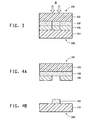
- Procédé de fabrication d'une couche métallique texturée ayant une conductivité élevée comprenant les étapes consistant à:fournir un substrat texturé comprenant une couche de catalyseur texturée sur un substrat de base; ledit substrat texturé étant préparé par un procédé d'imagerie thermique consistant à:(a) utiliser un donneur de transfert thermique (100) comprenant un film de base (102) et une couche de transfert de catalyseur (106), la couche de transfert de catalyseur (106) comprenant: (i) une fraction de catalyseur; éventuellement, (ii) une fraction de promoteur d'adhésion; et éventuellement et indépendamment, (iii) une fraction de liant polymère;(b) mettre en contact le donneur de transfert thermique (100) avec un receveur (200), le receveur (200) comprenant une couche de base (202); et(c) transférer au moins une partie de la couche de transfert de catalyseur (106) sur le receveur (200) par transfert thermique afin de fournir un receveur texturé représentant ledit substrat texturé; etplaquer un métal sur ledit substrat texturé, afin de fournir la couche métallique texturée (210) en relation avec la couche de catalyseur texturée.
- Procédé selon la revendication 1 dans lequel la couche de transfert de catalyseur (106) et la couche de catalyseur texturée comportent une fraction de promoteur d'adhésion choisie parmi la fritte de verre; les oxydes métalliques; les hydroxydes et alcoxydes métalliques; les hydroxydes et alcoxydes de silicium (silicates); et les polyols organiques.
- Procédé selon la revendication 1 dans lequel la fraction de catalyseur comprend un ou plusieurs catalyseurs choisis dans le groupe: (1) des particules métalliques; (2) des oxydes métalliques; (3) des complexes métalliques organiques; (4) des sels métalliques organiques; (5) des céramiques et autres poudres non conductrices revêtues de sels métalliques, d'oxydes métalliques, de complexes métalliques, de métal ou de carbone; et (6) du carbone sous toutes ses formes conductrices; chaque métal de (1) à (5) étant choisi dans le groupe constitué de: Ag, Cu, Au, Fé, Ni, Al, Pd, Pt, Ru, Rh, Os, Ir, Sn et leurs alliages.
- Procédé selon la revendication 1 dans lequel la couche de transfert de catalyseur (106) et la couche de catalyseur texturée comprennent 1,0 à 99% en poids de fraction de catalyseur; 0,5 à 10% en poids de fraction de promoteur d'adhésion; et 0,5 à 98,5% en poids de fraction de liant polymère.
- Procédé selon la revendication 1 dans lequel le transfert s'effectue par un transfert induit par laser et ledit laser a une longueur d'onde de travail de 350 à 1500 nm.
- Procédé selon la revendication 1 dans lequel le donneur de transfert thermique (100) comprend en outre une couche de conversion de lumière en chaleur (couche LTHC, 108), disposée entre le film de base (102) et la couche de transfert de catalyseur (106) comprenant un ou plusieurs absorbeurs de rayonnement choisis dans le groupe constitué de: films métalliques choisis parmi Cr et Ni; noir de carbone; graphite; et colorants absorbant dans le proche infrarouge avec des maxima d'absorption dans la plage de 600 à 1200 nm au sein de la couche LTHC (108).
- Procédé selon la revendication 1 dans lequel le procédé d'imagerie thermique consiste en outre à:(d) chauffer le substrat texturé à une température de recuisson pendant une période de recuisson pour fournir le substrat texturé recuit; et ledit placage de métal comprend le placage dudit substrat texturé recuit.
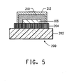
- Procédé selon la revendication 1 dans lequel ledit receveur (200) comprend en outre une couche antiréfléchissante texturée (204) ayant des limites; et ledit transfert d'au moins une partie de la couche de transfert de catalyseur (106) sur le receveur (200) se fait à l'intérieur des limites de la couche antiréfléchissante texturée (204).
- Procédé selon la revendication 1 dans lequel ledit donneur de transfert thermique (100) comprend en outre, sur la couche de transfert de catalyseur (106) opposée au film de base (102), une couche promotrice d'adhésion; et ledit transfert comprend en outre le transfert d'une partie proche correspondante de la couche promotrice d'adhésion afin de fournir ledit substrat texturé ayant, en couches successives sur ledit receveur, une couche promotrice d'adhésion texturée et ladite couche de catalyseur texturée.
- Procédé selon la revendication 1 dans lequel ledit receveur (200) comprend en outre une couche promotrice d'adhésion; et ledit transfert comprend le transfert d'au moins une partie de la couche de catalyseur (106) sur la couche promotrice d'adhésion dudit receveur (200).
- Donneur de transfert thermique (100) comprenant un film de base (102), une couche de transfert de catalyseur (A) (106), et une couche LTHC (108) intercalée entre ledit film de base (102) et ladite couche de transfert de catalyseur (A) (106), ladite couche de transfert de catalyseur (A) (106) comprenant:(i) 1,0 à 99% en poids d'une fraction de catalyseur (A), rapporté au poids total de la couche de catalyseur (106), ladite fraction de catalyseur comprenant des particules métalliques choisies parmi Ag, Cu, et leurs alliages;(ii) 0,5 à 10% en poids d'une fraction de promoteur d'adhésion choisie parmi les hydroxydes et alcoxydes métalliques;(iii) 0,5 à 98,5% en poids d'un liant polymère.
- Donneur (100) selon la revendication 11 dans lequel la couche LTHC (108) comprend un ou plusieurs absorbeurs de rayonnement choisis dans le groupe constitué de: films métalliques choisis parmi Cr et Ni; noir de carbone; graphite; et colorants absorbant dans le proche infrarouge avec des maxima d'absorption dans la plage de 600 à 1200 nm au sein de la couche LTHC (108).
- Donneur de transfert thermique (100) comprenant, en couches successives, un film de base (102), une couche de transfert de catalyseur (B) (106) et une couche promotrice d'adhésion, ladite couche de transfert de catalyseur (B) comprenant:(i) 1,0 à 99% en poids d'une fraction de catalyseur, rapporté au poids total de la couche de catalyseur (106), ladite fraction de catalyseur comprenant des particules métalliques choisies parmi Ag, Cu, et leurs alliages;(ii) 1,0 à 99% en poids d'un liant polymère; et
dans lequel la couche promotrice d'adhésion comprend un matériau choisi parmi la fritte de verre; et les hydroxydes et alcoxydes métalliques.
Applications Claiming Priority (2)
| Application Number | Priority Date | Filing Date | Title |
|---|---|---|---|
| US11/877,637 US7666568B2 (en) | 2007-10-23 | 2007-10-23 | Composition and method for providing a patterned metal layer having high conductivity |
| PCT/US2008/080851 WO2009055515A1 (fr) | 2007-10-23 | 2008-10-23 | Composition et procédé pour fournir une couche de métal dessinée ayant une conductivité élevée |
Publications (2)
| Publication Number | Publication Date |
|---|---|
| EP2200838A1 EP2200838A1 (fr) | 2010-06-30 |
| EP2200838B1 true EP2200838B1 (fr) | 2011-10-19 |
Family
ID=40219442
Family Applications (1)
| Application Number | Title | Priority Date | Filing Date |
|---|---|---|---|
| EP08842620A Not-in-force EP2200838B1 (fr) | 2007-10-23 | 2008-10-23 | Procédé pour fournir une couche de métal dessinée ayant une conductivité élevée |
Country Status (7)
| Country | Link |
|---|---|
| US (1) | US7666568B2 (fr) |
| EP (1) | EP2200838B1 (fr) |
| JP (1) | JP2011503348A (fr) |
| KR (1) | KR20100087018A (fr) |
| CN (1) | CN101835624B (fr) |
| AT (1) | ATE529266T1 (fr) |
| WO (1) | WO2009055515A1 (fr) |
Cited By (1)
| Publication number | Priority date | Publication date | Assignee | Title |
|---|---|---|---|---|
| RU2554608C2 (ru) * | 2013-07-01 | 2015-06-27 | Общество с ограниченной ответственностью "Солар" | Способ получения просветляющего покрытия |
Families Citing this family (40)
| Publication number | Priority date | Publication date | Assignee | Title |
|---|---|---|---|---|
| EP3056978A1 (fr) * | 2009-02-26 | 2016-08-17 | 3M Innovative Properties Company | Capteur d'écran tactile et substrat à motifs comprenant des micro-motifs superposés à faible visibilité |
| US20110279398A1 (en) * | 2010-05-12 | 2011-11-17 | Harald Philipp | Touch screen electrode enhancements |
| GB201009847D0 (en) * | 2010-06-11 | 2010-07-21 | Dzp Technologies Ltd | Deposition method, apparatus, printed object and uses |
| CN102465259A (zh) * | 2010-11-11 | 2012-05-23 | 鸿富锦精密工业(深圳)有限公司 | 塑料表面电磁屏蔽处理方法及其制品 |
| US10526198B2 (en) * | 2011-03-04 | 2020-01-07 | Texas Instruments Incorporated | Infrared sensor design using an epoxy film as an infrared absorption layer |
| JP6028727B2 (ja) * | 2011-05-18 | 2016-11-16 | 戸田工業株式会社 | 銅粉末、銅ペースト、導電性塗膜の製造方法及び導電性塗膜 |
| KR20130007042A (ko) * | 2011-06-28 | 2013-01-18 | 삼성디스플레이 주식회사 | 열전사용 도너 필름, 이의 제조 방법 및 이를 이용한 유기 발광 소자의 제조 방법 |
| CN103858059A (zh) * | 2011-10-14 | 2014-06-11 | 佳能株式会社 | 电子照相用构件、处理盒和电子照相设备 |
| CN103184440B (zh) * | 2011-12-27 | 2015-12-02 | 比亚迪股份有限公司 | 一种表面选择性金属化的制品及其制备方法 |
| TWI506752B (zh) * | 2012-04-18 | 2015-11-01 | Lg Chemical Ltd | 導電結構體及其製備方法 |
| KR101983691B1 (ko) * | 2012-08-17 | 2019-05-30 | 삼성디스플레이 주식회사 | 차광 부재 및 이를 포함하는 표시 장치 |
| JP5694265B2 (ja) * | 2012-10-02 | 2015-04-01 | 学校法人関東学院 | 無電解めっき方法及び無電解めっき膜 |
| KR101468690B1 (ko) * | 2012-11-19 | 2014-12-04 | 엔젯 주식회사 | 고점도 전도성 나노 잉크 조성물로 이루어진 전극선을 포함하는 투명전극 및 이를 이용한 터치센서, 투명히터 및 전자파 차폐제 |
| TW201445006A (zh) * | 2013-05-23 | 2014-12-01 | Byd Co Ltd | 聚合物製品表面選擇性金屬化方法及其製備的聚合物製品 |
| JP6275482B2 (ja) * | 2013-06-03 | 2018-02-07 | 株式会社レグルス | プラスチック製成形品への回路パターンの形成方法及びこれに用いる塗工液 |
| US9448666B2 (en) * | 2013-06-08 | 2016-09-20 | Microsoft Technology Licensing, Llc | Dark film lamination for a touch sensor |
| US9899117B2 (en) | 2013-06-24 | 2018-02-20 | University Of Houston System | Metallic nanomesh |
| JP6239647B2 (ja) * | 2013-08-01 | 2017-11-29 | エルジー・ケム・リミテッド | 3次元構造の金属パターンの製造方法 |
| JP6079505B2 (ja) | 2013-08-26 | 2017-02-15 | 三菱マテリアル株式会社 | 接合体及びパワーモジュール用基板 |
| EP3041045B1 (fr) * | 2013-08-26 | 2019-09-18 | Mitsubishi Materials Corporation | Corps collé et substrat de module de puissance |
| KR20150057032A (ko) * | 2013-11-18 | 2015-05-28 | 삼성전기주식회사 | 터치 패널 및 그의 제조 방법 |
| JP2015164030A (ja) * | 2014-01-31 | 2015-09-10 | 住友金属鉱山株式会社 | 導電性基板、積層導電性基板、導電性基板の製造方法、及び積層導電性基板の製造方法 |
| CN103935078B (zh) * | 2014-04-04 | 2016-08-24 | 刘从余 | 一种复合片材及其制备方法和设备 |
| JP5829746B1 (ja) * | 2014-04-04 | 2015-12-09 | キヤノン・コンポーネンツ株式会社 | 導電膜及びその製造方法並びにめっき皮膜付樹脂製品及びその製造方法 |
| JP6275861B2 (ja) * | 2014-09-29 | 2018-02-07 | 富士フイルム株式会社 | 積層体、導電性積層体およびその製造方法、タッチパネルセンサー、タッチパネル、転写フィルム |
| CN104294244B (zh) * | 2014-10-24 | 2017-05-31 | 中国科学院上海光学精密机械研究所 | 激光辅助化学混合镀实现二维表面金属结构的方法 |
| US20190053381A1 (en) * | 2014-11-28 | 2019-02-14 | Industrial Technology Research Institute | Structure of conductive lines and method of manufacturing the same |
| TWI584708B (zh) * | 2014-11-28 | 2017-05-21 | 財團法人工業技術研究院 | 導線結構及其製造方法 |
| KR102412896B1 (ko) | 2014-12-18 | 2022-06-24 | 삼성전자 주식회사 | 단말의 설비 제어를 지원하는 방법 및 장치 |
| CN107210097A (zh) * | 2014-12-26 | 2017-09-26 | 日本科技先进有限公司 | 在透明基板上具有图案化的导电性高分子层的层叠基板的制造方法以及金属网基板的制造方法 |
| WO2016127362A1 (fr) * | 2015-02-12 | 2016-08-18 | 四川大学华西医院 | Souris pour résonance magnétique et son procédé de fabrication, et appareil de transmission de signal |
| JP5843992B1 (ja) * | 2015-05-01 | 2016-01-13 | 株式会社イオックス | 無電解めっき用転写フィルム用触媒組成物及び無電解めっき用転写フィルム |
| KR20170012679A (ko) | 2015-07-22 | 2017-02-03 | 희성전자 주식회사 | 터치 센서의 제조 방법 및 이 방법으로 제조되는 터치 센서 |
| US9915002B2 (en) * | 2015-09-21 | 2018-03-13 | Ethan Pfeiffer | System and method for producing a nano metal mesh using a brittle film template for lithography |
| WO2017173281A1 (fr) * | 2016-03-31 | 2017-10-05 | Electro Scientific Industries, Inc. | Ensemencement par laser pour placage électro-conducteur |
| CN109492504B (zh) * | 2017-09-12 | 2023-07-04 | 江西欧迈斯微电子有限公司 | 超声波生物识别装置及其制备方法和电子设备 |
| TWI646672B (zh) | 2017-12-01 | 2019-01-01 | 財團法人工業技術研究院 | 紅外線感測元件及其製造方法 |
| US10519595B2 (en) | 2017-12-29 | 2019-12-31 | Industrial Technology Research Institute | Composite textile |
| EP3804140A2 (fr) * | 2018-06-07 | 2021-04-14 | Continental Automotive GmbH | Objet de couleur noire ayant une fonction de champ électromagnétique ou électrique |
| US11167375B2 (en) | 2018-08-10 | 2021-11-09 | The Research Foundation For The State University Of New York | Additive manufacturing processes and additively manufactured products |
Family Cites Families (25)
| Publication number | Priority date | Publication date | Assignee | Title |
|---|---|---|---|---|
| US4743091A (en) * | 1986-10-30 | 1988-05-10 | Daniel Gelbart | Two dimensional laser diode array |
| KR970707718A (ko) | 1987-04-06 | 1997-12-01 | 마사아끼 시마다 | 패턴 형성용 시이트(sheets for formation of patterms) |
| US5256506A (en) * | 1990-10-04 | 1993-10-26 | Graphics Technology International Inc. | Ablation-transfer imaging/recording |
| SE9200564L (sv) * | 1992-02-26 | 1993-03-15 | Perstorp Ab | Dendritisk makromolekyl av polyestertyp, foerfarande foer framstaellning daerav samt anvaendning daerav |
| SE503342C2 (sv) * | 1994-10-24 | 1996-05-28 | Perstorp Ab | Hyperförgrenad makromolekyl av polyestertyp samt förfarande för dess framställning |
| US5994489A (en) * | 1994-10-24 | 1999-11-30 | The Dow Chemical Company | Adhesion promoter and self-priming arylcyclobutene resin compositions |
| JP3585598B2 (ja) | 1995-08-25 | 2004-11-04 | 大日本印刷株式会社 | 熱転写シート |
| US6207268B1 (en) * | 1996-11-12 | 2001-03-27 | Dai Nippon Printing Co., Ltd. | Transfer sheet, and pattern-forming method |
| US6822068B2 (en) * | 1998-12-22 | 2004-11-23 | Bayer Aktiengesellschaft | Method for producing highly-branched glycidol-based polyols |
| SE514207C2 (sv) * | 1999-03-23 | 2001-01-22 | Perstorp Ab | Hyperförgrenad dendritisk polyeter och förfarande för framställning därav |
| WO2001047707A1 (fr) * | 1999-12-28 | 2001-07-05 | Nippon Shokubai Co., Ltd. | Materiau multicouche |
| US6228555B1 (en) * | 1999-12-28 | 2001-05-08 | 3M Innovative Properties Company | Thermal mass transfer donor element |
| US6645681B2 (en) * | 2000-12-15 | 2003-11-11 | E. I. Du Pont De Nemours And Company | Color filter |
| JP2002185184A (ja) | 2000-12-18 | 2002-06-28 | Dainippon Printing Co Ltd | 電磁波シールド材及びその製造方法 |
| JP4668438B2 (ja) * | 2001-03-08 | 2011-04-13 | 住友ゴム工業株式会社 | 電磁波シールド板及びその製造方法 |
| JP2003025510A (ja) * | 2001-07-16 | 2003-01-29 | Shin Etsu Chem Co Ltd | 反射防止性及び耐擦傷性を有する多層積層体 |
| CN1582151A (zh) * | 2001-09-08 | 2005-02-16 | 阿斯特拉曾尼卡有限公司 | 用于治疗高脂血症、具有回肠胆汁酸转运(ibat)抑制活性的苯并硫氮杂䓬和苯并硫杂二氮杂䓬衍生物 |
| US6767980B2 (en) * | 2002-04-19 | 2004-07-27 | Nippon Shokubai Co., Ltd. | Reactive diluent and curable resin composition |
| JP2005534046A (ja) | 2002-05-17 | 2005-11-10 | イー・アイ・デュポン・ドウ・ヌムール・アンド・カンパニー | カラーフィルタのサーマルプリンティングのドナー要素用の低分子量アクリルコポリマーラテックス |
| CA2485166A1 (fr) * | 2002-05-21 | 2003-12-04 | Amgen Inc. | Composes heterocycliques substitues et leurs procedes d'utilisation |
| CN100346003C (zh) * | 2002-07-12 | 2007-10-31 | 藤森工业株式会社 | 电磁波屏蔽材料及其制造方法 |
| KR100667067B1 (ko) * | 2004-09-08 | 2007-01-10 | 삼성에스디아이 주식회사 | 레이저 전사용 도너 기판 및 그 기판을 사용하여 제조되는유기 전계 발광 소자 |
| US7270887B2 (en) * | 2004-10-13 | 2007-09-18 | Shin-Etsu Chemical Co., Ltd. | Antireflective coating, coating composition, and antireflective coated article |
| US20080014532A1 (en) * | 2006-07-14 | 2008-01-17 | 3M Innovative Properties Company | Laminate body, and method for manufacturing thin substrate using the laminate body |
| US7927454B2 (en) * | 2007-07-17 | 2011-04-19 | Samsung Mobile Display Co., Ltd. | Method of patterning a substrate |
-
2007
- 2007-10-23 US US11/877,637 patent/US7666568B2/en not_active Expired - Fee Related
-
2008
- 2008-10-23 AT AT08842620T patent/ATE529266T1/de not_active IP Right Cessation
- 2008-10-23 EP EP08842620A patent/EP2200838B1/fr not_active Not-in-force
- 2008-10-23 WO PCT/US2008/080851 patent/WO2009055515A1/fr active Application Filing
- 2008-10-23 CN CN200880112842.9A patent/CN101835624B/zh not_active Expired - Fee Related
- 2008-10-23 JP JP2010531216A patent/JP2011503348A/ja not_active Abandoned
- 2008-10-23 KR KR1020107011123A patent/KR20100087018A/ko not_active Application Discontinuation
Cited By (1)
| Publication number | Priority date | Publication date | Assignee | Title |
|---|---|---|---|---|
| RU2554608C2 (ru) * | 2013-07-01 | 2015-06-27 | Общество с ограниченной ответственностью "Солар" | Способ получения просветляющего покрытия |
Also Published As
| Publication number | Publication date |
|---|---|
| EP2200838A1 (fr) | 2010-06-30 |
| ATE529266T1 (de) | 2011-11-15 |
| JP2011503348A (ja) | 2011-01-27 |
| CN101835624B (zh) | 2012-10-10 |
| KR20100087018A (ko) | 2010-08-02 |
| CN101835624A (zh) | 2010-09-15 |
| WO2009055515A1 (fr) | 2009-04-30 |
| US20090104572A1 (en) | 2009-04-23 |
| US7666568B2 (en) | 2010-02-23 |
Similar Documents
| Publication | Publication Date | Title |
|---|---|---|
| EP2200838B1 (fr) | Procédé pour fournir une couche de métal dessinée ayant une conductivité élevée | |
| EP2201827B1 (fr) | Procédé de formation d'images négatives pour fournir une couche métallique à motif présentant une conductivité élevée | |
| EP2176407B1 (fr) | Procédé de formation d'un motif sur un substrat | |
| US7901596B2 (en) | Metal compositions, thermal imaging donors and patterned multilayer compositions derived therefrom | |
| EP1216156B1 (fr) | Element de transfert thermique avec une couche de transfert contenant un plastifiant, et processus de transfert thermique | |
| EP2041626B1 (fr) | Procédé pour améliorer la résolution d'un motif transféré thermiquement | |
| EP2041814A2 (fr) | Eléments donneurs et procédés de transfert thermique de couches de nanoparticules | |
| WO2008010982A2 (fr) | Couches diélectriques imageables thermiquement et donneurs et receveurs de transfert thermique | |
| JP2014192465A (ja) | 電気回路配線基板の製造方法 | |
| KR20170133658A (ko) | 구리나노잉크 및 레이저 소결법을 이용하는 투명 전자파 차폐 필름 제조방법 | |
| JP2006035664A (ja) | 画像作製方法 |
Legal Events
| Date | Code | Title | Description |
|---|---|---|---|
| PUAI | Public reference made under article 153(3) epc to a published international application that has entered the european phase |
Free format text: ORIGINAL CODE: 0009012 |
|
| 17P | Request for examination filed |
Effective date: 20100413 |
|
| AK | Designated contracting states |
Kind code of ref document: A1 Designated state(s): AT BE BG CH CY CZ DE DK EE ES FI FR GB GR HR HU IE IS IT LI LT LU LV MC MT NL NO PL PT RO SE SI SK TR |
|
| AX | Request for extension of the european patent |
Extension state: AL BA MK RS |
|
| 17Q | First examination report despatched |
Effective date: 20101011 |
|
| DAX | Request for extension of the european patent (deleted) | ||
| GRAP | Despatch of communication of intention to grant a patent |
Free format text: ORIGINAL CODE: EPIDOSNIGR1 |
|
| RIC1 | Information provided on ipc code assigned before grant |
Ipc: H05K 9/00 20060101ALI20110307BHEP Ipc: H05K 3/18 20060101ALI20110307BHEP Ipc: H05K 3/04 20060101ALI20110307BHEP Ipc: B41M 5/382 20060101AFI20110307BHEP Ipc: B41M 5/392 20060101ALI20110307BHEP |
|
| RTI1 | Title (correction) |
Free format text: METHOD FOR PROVIDING A PATTERNED METAL LAYER HAVING HIGH CONDUCTIVITY |
|
| GRAS | Grant fee paid |
Free format text: ORIGINAL CODE: EPIDOSNIGR3 |
|
| GRAA | (expected) grant |
Free format text: ORIGINAL CODE: 0009210 |
|
| AK | Designated contracting states |
Kind code of ref document: B1 Designated state(s): AT BE BG CH CY CZ DE DK EE ES FI FR GB GR HR HU IE IS IT LI LT LU LV MC MT NL NO PL PT RO SE SI SK TR |
|
| REG | Reference to a national code |
Ref country code: GB Ref legal event code: FG4D |
|
| REG | Reference to a national code |
Ref country code: CH Ref legal event code: EP |
|
| REG | Reference to a national code |
Ref country code: IE Ref legal event code: FG4D |
|
| REG | Reference to a national code |
Ref country code: DE Ref legal event code: R096 Ref document number: 602008010654 Country of ref document: DE Effective date: 20111215 |
|
| REG | Reference to a national code |
Ref country code: NL Ref legal event code: VDEP Effective date: 20111019 |
|
| LTIE | Lt: invalidation of european patent or patent extension |
Effective date: 20111019 |
|
| REG | Reference to a national code |
Ref country code: AT Ref legal event code: MK05 Ref document number: 529266 Country of ref document: AT Kind code of ref document: T Effective date: 20111019 |
|
| PG25 | Lapsed in a contracting state [announced via postgrant information from national office to epo] |
Ref country code: BE Free format text: LAPSE BECAUSE OF FAILURE TO SUBMIT A TRANSLATION OF THE DESCRIPTION OR TO PAY THE FEE WITHIN THE PRESCRIBED TIME-LIMIT Effective date: 20111019 Ref country code: NO Free format text: LAPSE BECAUSE OF FAILURE TO SUBMIT A TRANSLATION OF THE DESCRIPTION OR TO PAY THE FEE WITHIN THE PRESCRIBED TIME-LIMIT Effective date: 20120119 Ref country code: IS Free format text: LAPSE BECAUSE OF FAILURE TO SUBMIT A TRANSLATION OF THE DESCRIPTION OR TO PAY THE FEE WITHIN THE PRESCRIBED TIME-LIMIT Effective date: 20120219 Ref country code: LT Free format text: LAPSE BECAUSE OF FAILURE TO SUBMIT A TRANSLATION OF THE DESCRIPTION OR TO PAY THE FEE WITHIN THE PRESCRIBED TIME-LIMIT Effective date: 20111019 |
|
| PG25 | Lapsed in a contracting state [announced via postgrant information from national office to epo] |
Ref country code: LV Free format text: LAPSE BECAUSE OF FAILURE TO SUBMIT A TRANSLATION OF THE DESCRIPTION OR TO PAY THE FEE WITHIN THE PRESCRIBED TIME-LIMIT Effective date: 20111019 Ref country code: SE Free format text: LAPSE BECAUSE OF FAILURE TO SUBMIT A TRANSLATION OF THE DESCRIPTION OR TO PAY THE FEE WITHIN THE PRESCRIBED TIME-LIMIT Effective date: 20111019 Ref country code: MC Free format text: LAPSE BECAUSE OF NON-PAYMENT OF DUE FEES Effective date: 20111031 Ref country code: SI Free format text: LAPSE BECAUSE OF FAILURE TO SUBMIT A TRANSLATION OF THE DESCRIPTION OR TO PAY THE FEE WITHIN THE PRESCRIBED TIME-LIMIT Effective date: 20111019 Ref country code: GR Free format text: LAPSE BECAUSE OF FAILURE TO SUBMIT A TRANSLATION OF THE DESCRIPTION OR TO PAY THE FEE WITHIN THE PRESCRIBED TIME-LIMIT Effective date: 20120120 Ref country code: HR Free format text: LAPSE BECAUSE OF FAILURE TO SUBMIT A TRANSLATION OF THE DESCRIPTION OR TO PAY THE FEE WITHIN THE PRESCRIBED TIME-LIMIT Effective date: 20111019 Ref country code: PT Free format text: LAPSE BECAUSE OF FAILURE TO SUBMIT A TRANSLATION OF THE DESCRIPTION OR TO PAY THE FEE WITHIN THE PRESCRIBED TIME-LIMIT Effective date: 20120220 Ref country code: NL Free format text: LAPSE BECAUSE OF FAILURE TO SUBMIT A TRANSLATION OF THE DESCRIPTION OR TO PAY THE FEE WITHIN THE PRESCRIBED TIME-LIMIT Effective date: 20111019 |
|
| PG25 | Lapsed in a contracting state [announced via postgrant information from national office to epo] |
Ref country code: CY Free format text: LAPSE BECAUSE OF FAILURE TO SUBMIT A TRANSLATION OF THE DESCRIPTION OR TO PAY THE FEE WITHIN THE PRESCRIBED TIME-LIMIT Effective date: 20111019 |
|
| PG25 | Lapsed in a contracting state [announced via postgrant information from national office to epo] |
Ref country code: BG Free format text: LAPSE BECAUSE OF FAILURE TO SUBMIT A TRANSLATION OF THE DESCRIPTION OR TO PAY THE FEE WITHIN THE PRESCRIBED TIME-LIMIT Effective date: 20120119 Ref country code: EE Free format text: LAPSE BECAUSE OF FAILURE TO SUBMIT A TRANSLATION OF THE DESCRIPTION OR TO PAY THE FEE WITHIN THE PRESCRIBED TIME-LIMIT Effective date: 20111019 Ref country code: DK Free format text: LAPSE BECAUSE OF FAILURE TO SUBMIT A TRANSLATION OF THE DESCRIPTION OR TO PAY THE FEE WITHIN THE PRESCRIBED TIME-LIMIT Effective date: 20111019 Ref country code: CZ Free format text: LAPSE BECAUSE OF FAILURE TO SUBMIT A TRANSLATION OF THE DESCRIPTION OR TO PAY THE FEE WITHIN THE PRESCRIBED TIME-LIMIT Effective date: 20111019 Ref country code: SK Free format text: LAPSE BECAUSE OF FAILURE TO SUBMIT A TRANSLATION OF THE DESCRIPTION OR TO PAY THE FEE WITHIN THE PRESCRIBED TIME-LIMIT Effective date: 20111019 |
|
| REG | Reference to a national code |
Ref country code: IE Ref legal event code: MM4A |
|
| PLBE | No opposition filed within time limit |
Free format text: ORIGINAL CODE: 0009261 |
|
| STAA | Information on the status of an ep patent application or granted ep patent |
Free format text: STATUS: NO OPPOSITION FILED WITHIN TIME LIMIT |
|
| PG25 | Lapsed in a contracting state [announced via postgrant information from national office to epo] |
Ref country code: RO Free format text: LAPSE BECAUSE OF FAILURE TO SUBMIT A TRANSLATION OF THE DESCRIPTION OR TO PAY THE FEE WITHIN THE PRESCRIBED TIME-LIMIT Effective date: 20111019 Ref country code: PL Free format text: LAPSE BECAUSE OF FAILURE TO SUBMIT A TRANSLATION OF THE DESCRIPTION OR TO PAY THE FEE WITHIN THE PRESCRIBED TIME-LIMIT Effective date: 20111019 Ref country code: IT Free format text: LAPSE BECAUSE OF FAILURE TO SUBMIT A TRANSLATION OF THE DESCRIPTION OR TO PAY THE FEE WITHIN THE PRESCRIBED TIME-LIMIT Effective date: 20111019 |
|
| 26N | No opposition filed |
Effective date: 20120720 |
|
| PG25 | Lapsed in a contracting state [announced via postgrant information from national office to epo] |
Ref country code: IE Free format text: LAPSE BECAUSE OF NON-PAYMENT OF DUE FEES Effective date: 20111023 |
|
| REG | Reference to a national code |
Ref country code: DE Ref legal event code: R097 Ref document number: 602008010654 Country of ref document: DE Effective date: 20120720 |
|
| PG25 | Lapsed in a contracting state [announced via postgrant information from national office to epo] |
Ref country code: AT Free format text: LAPSE BECAUSE OF FAILURE TO SUBMIT A TRANSLATION OF THE DESCRIPTION OR TO PAY THE FEE WITHIN THE PRESCRIBED TIME-LIMIT Effective date: 20111019 |
|
| PGFP | Annual fee paid to national office [announced via postgrant information from national office to epo] |
Ref country code: FR Payment date: 20121018 Year of fee payment: 5 Ref country code: DE Payment date: 20121017 Year of fee payment: 5 |
|
| PG25 | Lapsed in a contracting state [announced via postgrant information from national office to epo] |
Ref country code: MT Free format text: LAPSE BECAUSE OF FAILURE TO SUBMIT A TRANSLATION OF THE DESCRIPTION OR TO PAY THE FEE WITHIN THE PRESCRIBED TIME-LIMIT Effective date: 20111019 |
|
| PGFP | Annual fee paid to national office [announced via postgrant information from national office to epo] |
Ref country code: GB Payment date: 20121017 Year of fee payment: 5 |
|
| PG25 | Lapsed in a contracting state [announced via postgrant information from national office to epo] |
Ref country code: ES Free format text: LAPSE BECAUSE OF FAILURE TO SUBMIT A TRANSLATION OF THE DESCRIPTION OR TO PAY THE FEE WITHIN THE PRESCRIBED TIME-LIMIT Effective date: 20120130 |
|
| PG25 | Lapsed in a contracting state [announced via postgrant information from national office to epo] |
Ref country code: LU Free format text: LAPSE BECAUSE OF NON-PAYMENT OF DUE FEES Effective date: 20111023 |
|
| REG | Reference to a national code |
Ref country code: CH Ref legal event code: PL |
|
| PG25 | Lapsed in a contracting state [announced via postgrant information from national office to epo] |
Ref country code: FI Free format text: LAPSE BECAUSE OF FAILURE TO SUBMIT A TRANSLATION OF THE DESCRIPTION OR TO PAY THE FEE WITHIN THE PRESCRIBED TIME-LIMIT Effective date: 20111019 |
|
| PG25 | Lapsed in a contracting state [announced via postgrant information from national office to epo] |
Ref country code: CH Free format text: LAPSE BECAUSE OF NON-PAYMENT OF DUE FEES Effective date: 20121031 Ref country code: LI Free format text: LAPSE BECAUSE OF NON-PAYMENT OF DUE FEES Effective date: 20121031 |
|
| PG25 | Lapsed in a contracting state [announced via postgrant information from national office to epo] |
Ref country code: TR Free format text: LAPSE BECAUSE OF FAILURE TO SUBMIT A TRANSLATION OF THE DESCRIPTION OR TO PAY THE FEE WITHIN THE PRESCRIBED TIME-LIMIT Effective date: 20111019 |
|
| PG25 | Lapsed in a contracting state [announced via postgrant information from national office to epo] |
Ref country code: HU Free format text: LAPSE BECAUSE OF FAILURE TO SUBMIT A TRANSLATION OF THE DESCRIPTION OR TO PAY THE FEE WITHIN THE PRESCRIBED TIME-LIMIT Effective date: 20111019 |
|
| GBPC | Gb: european patent ceased through non-payment of renewal fee |
Effective date: 20131023 |
|
| PG25 | Lapsed in a contracting state [announced via postgrant information from national office to epo] |
Ref country code: GB Free format text: LAPSE BECAUSE OF NON-PAYMENT OF DUE FEES Effective date: 20131023 |
|
| REG | Reference to a national code |
Ref country code: FR Ref legal event code: ST Effective date: 20140630 |
|
| REG | Reference to a national code |
Ref country code: DE Ref legal event code: R119 Ref document number: 602008010654 Country of ref document: DE Effective date: 20140501 |
|
| PG25 | Lapsed in a contracting state [announced via postgrant information from national office to epo] |
Ref country code: DE Free format text: LAPSE BECAUSE OF NON-PAYMENT OF DUE FEES Effective date: 20140501 Ref country code: FR Free format text: LAPSE BECAUSE OF NON-PAYMENT OF DUE FEES Effective date: 20131031 |