EP2197200A2 - Bildaufnahmevorrichtung und Bildaufnahmesystem - Google Patents
Bildaufnahmevorrichtung und Bildaufnahmesystem Download PDFInfo
- Publication number
- EP2197200A2 EP2197200A2 EP09178810A EP09178810A EP2197200A2 EP 2197200 A2 EP2197200 A2 EP 2197200A2 EP 09178810 A EP09178810 A EP 09178810A EP 09178810 A EP09178810 A EP 09178810A EP 2197200 A2 EP2197200 A2 EP 2197200A2
- Authority
- EP
- European Patent Office
- Prior art keywords
- processing
- signal
- readout circuit
- image
- converters
- Prior art date
- Legal status (The legal status is an assumption and is not a legal conclusion. Google has not performed a legal analysis and makes no representation as to the accuracy of the status listed.)
- Withdrawn
Links
Images




Classifications
-
- H—ELECTRICITY
- H04—ELECTRIC COMMUNICATION TECHNIQUE
- H04N—PICTORIAL COMMUNICATION, e.g. TELEVISION
- H04N25/00—Circuitry of solid-state image sensors [SSIS]; Control thereof
- H04N25/60—Noise processing, e.g. detecting, correcting, reducing or removing noise
-
- H—ELECTRICITY
- H04—ELECTRIC COMMUNICATION TECHNIQUE
- H04N—PICTORIAL COMMUNICATION, e.g. TELEVISION
- H04N25/00—Circuitry of solid-state image sensors [SSIS]; Control thereof
- H04N25/30—Circuitry of solid-state image sensors [SSIS]; Control thereof for transforming X-rays into image signals
-
- H—ELECTRICITY
- H04—ELECTRIC COMMUNICATION TECHNIQUE
- H04N—PICTORIAL COMMUNICATION, e.g. TELEVISION
- H04N25/00—Circuitry of solid-state image sensors [SSIS]; Control thereof
- H04N25/70—SSIS architectures; Circuits associated therewith
- H04N25/76—Addressed sensors, e.g. MOS or CMOS sensors
- H04N25/78—Readout circuits for addressed sensors, e.g. output amplifiers or A/D converters
Definitions
- the present invention relates to an image pickup apparatus, a radiation image pickup apparatus, more particularly an image pickup apparatus and a radiation image pickup apparatus that are capable of reading a signal from a flat panel detector as digital output using a plurality of analog-to-digital (A/D).
- A/D analog-to-digital
- a radiation image pickup apparatus employing a flat panel detector (hereinafter abbreviated as FPD) made of a semiconductor material has been becoming practical as an imaging apparatus for use in medical image diagnosis and nondestructive inspection using X rays.
- FPD flat panel detector
- Such a radiation image pickup apparatus employing an FPD is an apparatus that can perform digital imaging of converting radiation, for example, an X ray that transmitted through an object (e.g., patient) into an analog electric signal using the FPD and converting the analog electric signal into a digital image signal.
- FPDs used in such a radiation image pickup apparatus can be broadly classified into the direct conversion type and the indirect conversion type.
- a direct-conversion radiation image pickup apparatus is an apparatus that includes an FPD having a plurality of pixels two-dimensionally arranged, each pixel including a conversion element made of a semiconductor material that can directly convert radiation into an electrical charge (e.g., a-Se).
- An indirect-conversion radiation image pickup apparatus is an apparatus that includes an FPD having a plurality of pixels two-dimensionally arranged, each pixel including a conversion element that has a wavelength conversion member that can convert radiation into light (e.g., fluorescent member) and that has a photoelectric conversion element made of a semiconductor material that can convert light into an electrical charge (e.g., a-Si).
- Such radiation image pickup apparatuses employing FPDs are used as digital image pickup apparatuses capable of radiographic imaging, like still imaging, and movie imaging, like fluoroscopy imaging.
- a correction image signal for use in correction of the image signal in image capturing is obtained from a radiation image pickup apparatus.
- a correction signal for use in offset correction is based on output obtained in a state where no light or radiation is applied to a detector (dark output).
- a correction signal for use in sensitivity correction is based on output obtained in a state where light or radiation is applied to a detector in a substantially uniform manner (bright output). Correcting an image signal in image capturing using such a correction image signal enables the image signal to have low noise and high precision.
- the radiation image pickup apparatus includes the above-described detector, a driving circuit for driving the detector, a readout circuit for reading an analog electric signal from the detector, and an A/D converter for converting the analog electric signal into a digital signal.
- the A/D converter outputs a digitized image signal in image capturing and a correction image signal.
- the image pickup apparatus includes a plurality of A/D converters.
- a conversion characteristic between an input analog electric signal and an output digital signal in an A/D converter may have nonlinearity that does not exhibit ideal linearity.
- the A/D converters may have different nonlinearities, and an image formed from a digital signal may have artifact, such as a step.
- artifact such as a step, occurs, the nonlinearities should be reduced or effects caused by nonlinearities should be compensated for.
- Japanese Patent Laid-Open No. 2005-210480 discloses an A/D converter circuit that stores, at an address specified by an output from an A/D conversion unit, a reference signal synchronized using an output signal from the A/D conversion unit as address data and that corrects the output signal from the A/D conversion unit in accordance with the reference signal.
- the patent document discloses the capability to reduce artifact in image caused by nonlinearity of the A/D conversion unit and to achieve high image quality by use of the above configuration.
- Japanese Patent Laid-Open No. 2005-210396 discloses an A/D converter circuit that includes a correcting unit configured to correct output signals from a plurality of A/D conversion units in accordance with an output signal from either one of the plurality of A/D conversion units.
- the patent document discloses the capability to reduce artifact in image caused by difference between nonlinearities of the plurality of A/D conversion units and to achieve high image quality by use of the above configuration.
- the present invention provides an image pickup apparatus and an image pickup system that are capable of reducing artifact, such as a step, in image resulting from difference between nonlinearities of a plurality of A/D converters using a simple configuration and uncomplicated processing.
- the present invention in its first aspect provides an apparatus as specified in claims 1 to 9.
- the present invention in its second aspect provides an image pickup system as specified in claim 10.
- the present invention in its third aspect provides a method as specified in claims 11 to 20.
- an image pickup apparatus and an image pickup system that are capable of reducing artifact, such as a step, in image resulting from difference between nonlinearities of a plurality of A/D converters using a simple configuration and uncomplicated processing can be provided.
- Fig. 1 is a conceptual block diagram of an image pickup apparatus according to a first embodiment of the present invention.
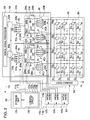
- Fig. 2 is a conceptual diagram of an image pickup system, the conceptual diagram containing an equivalent circuit diagram of the image pickup apparatus according to the first embodiment of the present invention.
- Figs. 3A and 3B illustrate characteristics for use in describing effects caused by difference between A/D conversion characteristics of A/D converters.
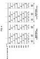
- Fig. 4 is a timing chart for use in describing operations of the image pickup apparatus according to the first embodiment of the present invention.
- Fig. 5 is a conceptual diagram of an image pickup system, the conceptual diagram containing an equivalent circuit diagram of an image pickup apparatus according to a second embodiment of the present invention.
- Fig. 6 is a timing chart for use in describing operations of the image pickup apparatus according to the second embodiment of the present invention.
- Figs. 7A and 7B are conceptual diagrams of radiation image pickup systems that employ an image pickup apparatus according to the present invention.
- radiation is described as including electromagnetic waves, such as X-rays and gamma rays, alpha rays, and beta rays.
- FIG. 1 is a conceptual block diagram of an image pickup apparatus according to a first embodiment of the present invention.
- An image pickup apparatus 100 illustrated in Fig. 1 includes a detector 101 having a plurality of pixels arranged in a matrix, each pixel being configured to convert radiation or light into an analog electric signal, and a driving circuit 102 configured to drive the detector 101 in order to make the detector 101 output an analog electric signal.
- the detector 101 has a form having pixels of 8 rows by 8 columns, and the pixels are divided into a first pixel group 101a and a second pixel group 101b, each pixel group having 4 pixel columns as one set.
- An analog electric signal output from the first pixel group 101a is read by an associated first readout circuit 103a.
- An analog electric signal 113 from the first readout circuit 103a is converted into a digital signal 114 by an associated first A/D converter 104a.
- an analog electric signal from the second pixel group 101b is read by an associated second readout circuit 103b and converted by an associated second A/D converter 104b into a digital signal.
- the digital signals from the first and second A/D converters 104a and 104b are subjected to simple digital signal processing, such as digital multiplex processing or offset correction, by a digital signal processor 105, and the processed digital signal is output.
- a signal processing device 106 includes a readout circuit portion 103 including the first and second readout circuits 103a and 103b, an A/D converting portion 104 including the first and second A/D converters 104a and 104b, and the digital signal processor 105.
- the image pickup apparatus 100 further includes a power supply portion 107 configured to supply the components included in the signal processing device 106 with respective biases.
- the power supply portion 107 includes first and second reference supplies 107a and 107b configured to supply the readout circuit portion 103 with a reference voltage and a third reference supply 107c configured to supply the A/D converting portion 104 with a reference voltage.
- the image pickup apparatus 100 further includes a controller 110 configured to control at least one of the signal processing device 106 and the power supply portion 107.
- the controller 110 includes a storage unit 109 in which information relating to nonlinearity of each of the first and second A/D converters 104a and 104b and a control circuit 108 configured to control at least one of the signal processing device 106 and the power supply portion 107 on the basis of the information.
- the control circuit 108 supplies the first and second reference supplies 107a and 107b with first and second reference voltage adjusting signals 118a and 118b, respectively, and supplies the third reference supply 107c with a third reference voltage adjusting signal 118c.
- the control circuit 108 also supplies the readout circuit portion 103 with gain adjusting signals 116a, 116b, 117a, and 117b and control signals 120a and 120b.
- the control circuit 108 also supplies the driving circuit 102 with a drive control signal 119. In response to the signal, the driving circuit 102 supplies the detector 101 with a driving signal 111.
- Fig. 2 is a conceptual diagram of an image pickup system, the conceptual diagram containing a conceptual equivalent circuit diagram of the image pickup apparatus according to the first embodiment of the present invention.
- the same reference numerals are used in components having the same configurations as ones described using Fig. 1 , and the detailed description thereof is omitted.
- the detector 101 includes pixels 201 arranged in a matrix.
- the 8 ⁇ 8 pixels 201 arranged in a matrix with 8 rows by 8 columns are arranged.
- Each of the pixels 201 includes a conversion element S for converting radiation or light into an electrical charge and a switching element T for outputting an electric signal corresponding to the electrical charge.
- a photoelectric conversion element such as a PIN photodiode whose principal material is amorphous silicon and being arranged on an insulating substrate (e.g., glass substrate)
- an indirect conversion element including a wavelength conversion member being at the radiation entry side of the photoelectric conversion element and being for converting radiation into light that can be sensed by the photoelectric conversion element and a direct conversion element for directly converting radiation into an electrical charge can be suitably used.
- the switching element T a transistor including a control terminal and two main terminals can be suitably used; in the case of a pixel in which a photoelectric conversion element is disposed on an insulating substrate, a thin-film transistor (TFT) can be suitably used.
- the conversion element S includes a first electrode electrically connected to one of the two main terminals of the switching element T and a second electrode electrically connected to a bias power supply through common wiring.
- T 11 to T 18 For switching elements of a plurality of pixels in the row direction, for example, T 11 to T 18 , their control terminals are commonly electrically connected to driving wiring G 1 in the first row, and a driving signal for controlling a conductive state of each of the switching elements is supplied from the driving circuit 102 through the driving wiring on a row-by-row basis.
- their second main terminals are electrically connected to signal wiring Sig 1 in the first column, and, during the conductive state, electric signals corresponding to electrical charges of the conversion elements are output to the readout circuit portion 103 through the signal wiring.
- the detector 101 is divided into the first pixel group 101a and the second pixel group 101b, each pixel group having four pixel columns as one set. Analog electric signals output from the first pixel group 101a are read in parallel by the associated first readout circuit 103a in the readout circuit portion 103, whereas analog electric signals output from the second pixel group 101b are read in parallel by the associated second readout circuit 103b.
- the first readout circuit 103a includes a first amplifier circuit section 202a configured to amplify electric signals output in parallel from the first pixel group 101a and a first sample-and-hold circuit section 203a configured to sample and hold electric signals from the first amplifier circuit section 202a.
- the second readout circuit 103b includes a second amplifier circuit section 202b and a second sample-and-hold circuit section 203b.
- Each of the first and second amplifier circuit sections 202a and 202b includes an amplifier circuit for each signal wiring, the amplifier circuit including an operational amplifier 'A' configured to amplify a read electric signal and output it, an integration capacitor group Cf, a switch group SW configured to switch an amplification factor, and a reset switch RC configured to reset the integration capacitors.
- An output electric signal is input into an inverting input terminal of the operational amplifier A, and an amplified electric signal is output from an output terminal.
- a reference voltage Vref1a is input from the first reference supply 107a into a non-inverting input terminal of each of the amplifier circuits in odd-numbered columns
- a reference voltage Vref1b is input from the first reference supply 107a into a non-inverting input terminal of each of the amplifier circuits in even-numbered columns.
- the integration capacitor group Cf having a plurality of integration capacitors arranged in parallel is disposed between the inverting input terminal and the output terminal of the operational amplifier A.
- Each of the first and second sample-and-hold circuit sections 203a and 203b includes a sample-and-hold circuit for each amplifier circuit, the sample-and-hold circuit being made up of a sampling switch SH and a sampling capacitor Ch.
- the first and second readout circuits 103a and 103b further include first and second multiplexers 204a and 204b, respectively.
- Each of the first and second multiplexers 204a and 204b is configured to sequentially output electric signals read in parallel from the first or second sample-and-hold circuit section as image signals being serial signals.
- the first and second readout circuits 103a and 103b further include first and second variable amplifiers 205a and 205b, respectively.
- Each of the first and second variable amplifiers 205a and 205b is an output buffer configured to impedance-convert an image signal and output it.
- the first multiplexer 204a and the second multiplexer 204b include switches MS1 to MS4 and switches MS5 to MS8, respectively, corresponding to each signal wiring, and parallel signals are converted into serial signals by sequential selection of the switches.
- the first variable amplifier 205a includes an operational amplifier Aa configured to amplify an electric signal from the first multiplexer 204a and output it, an integration capacitor group Cfa, a switch group SWa configured to switch an amplification factor, and a reset switch RCa configured to reset the integration capacitors.
- the second variable amplifier 205b includes an operational amplifier Ab, an integration capacitor group Cfb, a switch group SWb configured to switch an amplification factor, and a reset switch RCb configured to reset the integration capacitors.
- a reference voltage Vref2a is input from the second reference supply 107b into a non-inverting input terminal of the first variable amplifier 205a
- a reference voltage Vref2b is input from the second reference supply 107b into a non-inverting input terminal of the second variable amplifier 205b.
- a reference voltage Vref3a is input from the third reference supply 107c into the first A/D converter 104a associated with the first readout circuit 103a, whereas a reference voltage Vref3b is input from the third reference supply 107c into the second A/D converter 104b associated with the second readout circuit 103b.
- the control circuit 108 supplies the gain adjusting signal 116a and the gain adjusting signal 116b to the amplifier circuits in odd-numbered columns and the amplifier circuits in even-numbered columns, respectively, among the plurality of amplifier circuits included in the first and second amplifier circuit sections 202a and 202b.
- the control circuit 108 supplies the first variable amplifier 205a with the gain adjusting signal 117a and supplies the second variable amplifier 205b with the gain adjusting signal 117b.
- the control circuit 108 controls at least one of the signal processing device 106 and the power supply portion 107 on the basis of information stored in the storage unit 109, which stores information regarding nonlinearity of each of the first and second A/D converters 104a and 104b.
- the control circuit 108 supplies the first multiplexer 204a with the control signal 120a and supplies the second multiplexer 204b with the control signal 120b.
- nonlinearity indicates how much the relationship between actual analog input and digital output (A/D conversion value) deviates from an ideal line and is specifically represented by differential nonlinearity (DNL) or integral nonlinearity (INL).
- INL means a deviation of, when an input-output characteristic of an A/D converter is viewed as a whole, an actual input-output characteristic from an ideal input-output line.
- DNL means a deviation of, when input-output stages are individually viewed, each stage from its ideal stage.
- FIG. 3A First, nonlinearity of each of the first and second A/D converters 104a and 104b is illustrated using Fig. 3A .
- the horizontal axis indicates an input voltage input into an A/D converter
- the vertical axis indicates a digital value (code) output from the A/D converter.
- Fig. 3A is an illustration with the assumption that the A/D converter has a resolution of 8 bits.
- Fig. 3B illustrates a difference between digital values with respect to input voltages of the first and second A/D converters 104a and 104b.
- a maximum output difference between the digital values of the A/D converters is approximately 30 LSB. Therefore, a maximum difference in an image of approximately 30 LSB may occur between the first and second pixel groups 101a and 101b associated with the first and second A/D converters 104a and 104b, respectively.
- the first and second pixel groups divide all the region of the detector 101, it results in a visually highly noticeable difference occurring in the border between the first and second pixel groups, so the quality of an obtained image significantly decreases.
- the controller 110 performs processing of altering an analog electric signal capable of being input into at least one of the first and second A/D converters or altering an A/D conversion characteristic of at least one of the first and second A/D converters.
- the controller 110 performs processing on an analog electric signal from the pixels in odd-numbered columns among the plurality of pixels included in the first or second pixel group, the processing being different from alteration of an analog electric signal from the pixels in even-numbered columns.
- an analog electric signal from a predetermined pixel is subjected to processing different from alteration of an analog electric signal from another pixel different from the predetermined pixel.
- a reference voltage to be supplied to each of the first and second A/D converters is subjected to alteration processing. Such processing causes variations in analog electric signal in the row direction, and the variations produce an output difference in digital output value within pixel groups.
- the output difference within pixel groups makes the output difference at the border between pixel groups less noticeable, so the difference is less noticeable than that occurring when the processing is not performed. This depends on visual features of a person who observes an image. Because of visual filtering effects, a step between pixel groups is identified more easily than a difference between analog electric signals between unit pixel columns, so the benefit of improving an image quality is high.
- the controller 110 performs at least one of processing described below.
- the controller 110 may have to control the first reference supply 107a.
- the first reference supply 107a alters at least one of the reference voltage Vref1a to be supplied to an amplifier circuit associated with a predetermined pixel column and the reference voltage Vref1b to be supplied to another amplifier circuit associated with a different pixel column different from the predetermined pixel column such that the reference voltages Vref1a and Vref1b have different voltage values.
- an odd-numbered pixel column can be adopted as the predetermined pixel column
- an even-numbered pixel column can be adopted as the different pixel column.
- the controller 110 may have to control the second reference supply 107b.
- the second reference supply 107b alters at least one of the reference voltage Vref2a to be supplied to the first variable amplifier 205a and the reference voltage Vref2b to be supplied to the second variable amplifier 205b such that the reference voltages Vref2a and Vref2b have different voltage values.
- This alteration is performed in synchronization with an operation of converting parallel signals into serial signals and outputting them as image signals, the operation being carried out by the first and second multiplexers. For example, in the case of Fig. 2 , it is performed in synchronization with an operation of selecting the switches MS1 to MS4 and MS5 to MS8 included in the first and second multiplexers corresponding to the signal wiring Sig 1 to Sig 8 .
- the controller 110 alters at least one of an amplification factor of an amplifier circuit associated with a predetermined pixel column and an amplification factor of an amplifier circuit associated with a different pixel column different from the predetermined pixel column such that the amplification factors are different, as needed.
- the controller 110 controls the amplification factors by supplying the gain adjusting signal 116a to a switch group of an amplifier circuit associated with an odd-numbered pixel column and supplying the gain adjusting signal 116b to a switch group of an amplifier circuit associated with an even-numbered pixel column.
- the controller 110 alters at least one of an amplification factor of the first variable amplifier 205a and an amplification factor of the second variable amplifier 205b such that the amplification factors are different, as needed. This alteration is also performed in synchronization with an operation carried out by the first and second multiplexers, as in the second processing.
- the controller 110 controls the third reference supply 107c as needed in order to shift at least one of the levels of the A/D conversion characteristics of the first and second A/D converters 104a and 104b.
- the third reference supply 107c alters at least one of the reference voltage Vref3a to be supplied to the first A/D converter 104a and the reference voltage Vref3b to be supplied to the second A/D converter 104b such that the reference voltages Vref3a and Vref3b have different voltage values. This alteration is also performed in synchronization with an operation carried out by the first and second multiplexers, as in the second processing.
- the controller 110 perform the above-described processing on the basis of information regarding nonlinearity of each of the first and second A/D converters 104a and 104b stored in the storage unit 109.
- the processing can be performed such that, on the basis of that information, a difference between a mean value of digital signals output from the first A/D converter 104a and a mean value of digital signals output from the second A/D converter 104b is reduced. This enables processing of reducing a difference with higher precision.
- an unnecessary signal component is added to an image signal to be obtained, so accuracy of the obtained image signal may decrease.
- an image signal in image capturing and a correction image signal for use in correction of the image signal in image capturing are obtained by substantially the same processing.
- the digital signal processor 105 performs correction using the obtained correction image signal and the obtained image signal in image capturing and outputs the corrected image signal.
- Fig. 4 is a timing chart for use in describing an operation of the image pickup apparatus when the second processing is used in obtainment of an image signal in image capturing and in obtainment of an offset correction image signal.
- the switch MS1 of the first multiplexer 204a and the switch MS5 of the second multiplexer 204b are selected at substantially the same timing.
- the switches MS2 and MS6, the switches MS3 and MS7, and the switches MS4 and MS8 are selected at substantially the same respective timings.
- Such selection enables signals to be read in parallel from the first and second pixel groups 101a and 101b, so the speed of reading can be enhanced.
- a reference voltage to be supplied to each of the first and second variable amplifiers is controlled using the second reference voltage adjusting signal 118b in synchronization with an operation of selecting a switch included in the first and second multiplexers.
- the control is performed such that when a switch in an odd-numbered column is selected, the reference voltage is set higher than a preset reference voltage; when a switch in an even-numbered column is selected, the preset reference voltage is used.
- an image signal in image capturing is obtained, in a period of time substantially the same as the period of time of the application of the previous pulse of radiation, a dark-time output based on an electrical charge generated by a conversion element when no radiation is applied to the image pickup apparatus is obtained, i.e., an offset correction image signal is obtained. Also in obtaining such an offset correction image signal, substantially the same processing is performed as in obtaining an image signal in image capturing. An offset correction is carried out by subtracting the offset correction image signal from the obtained image signal in image capturing, so the corrected image signal is obtained.
- the amount of change in reference voltage supplied to each variable amplifier may be determined in real time by the controller 110 using calculation based on information stored in the storage unit 109, or it may be determined in advance based on information regarding nonlinearity of each of the first and second A/D converters.
- an offset correction image signal is obtained after an image signal in image capturing is obtained.
- an offset correction image signal may be obtained in advance through processing, and an image signal in image capturing may be obtained through substantially the same processing.
- A/D conversion is carried out using two different ways of alteration processing, in which one corresponds to an even-numbered column and the other corresponds to an odd-numbered column. It is useful that more than two ways, for example, four ways be adopted. In addition, it is useful that the embodiment of the present invention be applied to an A/D converter whose structure tends to cause nonlinear error, such as a pipeline A/D converter.
- two A/D converters are used.
- the embodiment of the present invention may be applied to the case where more than two A/D converters are used.
- all A/D converters be subjected to alteration processing, only part of the plurality of A/D converters can be subjected to alteration processing.
- variable power supply such as one capable of simply outputting two voltage values or one including a D/A converter and capable of achieving finer adjustment, can be suitably used.
- FIG. 5 is a conceptual diagram of an image pickup system, the conceptual diagram containing an equivalent circuit diagram of an image pickup apparatus according to a second embodiment of the present invention.
- the same reference numerals are used in components having the same configurations as ones described in the first embodiment, and the detailed description thereof is omitted.
- an analog electric signal from a predetermined pixel is subjected to processing different from alteration of an analog electric signal from a different pixel from the predetermined pixel.
- a reference voltage to be supplied to each of the first and second A/D converters is subjected to alteration processing.
- processing different from alteration of an analog electric signal from a pixel included in the second pixel group is performed on an analog electric signal from a pixel included in the first pixel group.
- processing different from alteration of an A/D conversion characteristic of the second A/D converter is performed on the first A/D converter. That is, this processing reduces a difference being the difference between a mean value of image signals obtained from the first pixel group and a mean value of image signals obtained from the second pixel group, as compared with the case in which no such processing is performed. That is, the processing is performed for each readout circuit or each A/D converter associated with each pixel group so as to reduce an output difference between a plurality of A/D converters.
- the controller 110 supplies the first amplifier circuit section 202a with a gain adjusting signal 116a' and supplies the second amplifier circuit section 202b with a gain adjusting signal 116b'.
- the first reference supply 107a supplies the first amplifier circuit section 202a with the reference voltage Vref1a and supplies the second amplifier circuit section 202b with the reference voltage Vref1b.
- Such processing reduces the difference between mean values of image signals associated with pixel groups and results in a reduction in difference, as compared with the case in which no such processing is performed.
- the controller 110 carries out at least one of processing described below.
- the controller 110 controls the first reference supply 107a as needed.
- the first reference supply 107a alters at least one of the reference voltage Vref1a to be supplied to the first amplifier circuit section 202a and the reference voltage Vref1b to be supplied to the second amplifier circuit section 202b such that the reference voltages Vref1a and Vref1b have different voltage values.
- the controller 110 controls the second reference supply 107b as needed.
- the second reference supply 107b alters at least one of the reference voltage Vref2a to be supplied to the first variable amplifier 205a and the reference voltage Vref2b to be supplied to the second variable amplifier 205b such that the reference voltages Vref2a and Vref2b have different voltage values.
- the controller 110 alters at least one of an amplification factor of the first amplifier circuit section 202a and an amplification factor of the second amplifier circuit section 202b such that the amplification factors are different, as needed.
- the controller 110 alters at least one of an amplification factor of the first variable amplifier 205a and an amplification factor of the second variable amplifier 205b such that the amplification factors are different, as needed.
- the controller 110 controls the third reference supply 107c as needed in order to shift at least one of the levels of the A/D conversion characteristics of the first and second A/D converters 104a and 104b.
- the third reference supply 107c alters at least one of the reference voltage Vref3a to be supplied to the first A/D converter 104a and the reference voltage Vref3b to be supplied to the second A/D converter 104b such that the reference voltages Vref3a and Vref3b have different voltage values.
- the controller 110 perform the above-described processing on the basis of information regarding nonlinearity of each of the first and second A/D converters 104a and 104b stored in the storage unit 109.
- the above-described processing is performed so as to reduce a difference being the difference between a mean value of digital signals output from the first A/D converter and a mean value of digital signals output from the second A/D converter, as compared with the case in which no such processing is performed. This enables reduction in difference with higher precision.
- the case is described below in which the above second processing is performed in obtaining a correction image signal for offset correction using the first and second A/D converters 104a and 104b having the characteristics illustrated in Fig. 3A .
- a case is discussed where a predetermined reference voltage is supplied to each of the first and second variable amplifiers 205a and 205b and, for example, offset correction image signals having a mean value of approximately 0.2 (V) are output from the first and second variable amplifiers.
- processing is performed such that a reference voltage to be supplied to the second variable amplifier 205b is lower than a predetermined reference voltage and offset correction image signals having a mean value of approximately 0.1 (V) are output from the second variable amplifier 205b.
- This enables reduction in difference between mean values of digital signals output from the first and second A/D converters. It is to be noted that, when information regarding nonlinearity of each of the first and second A/D converters is obtained in advance, the processing may be set in advance.
- an image signal in image capturing and a correction image signal for use in correction of the image signal in image capturing are obtained by substantially the same processing such that they have substantially the amount of change, as in the case of the first embodiment.
- the digital signal processor 105 performs correction using the obtained correction image signal and the obtained image signal in image capturing and outputs the corrected image signal.
- Such processing enables an image whose added unnecessary signal component is removed or reduced, artifact, such as a step, is reduced, and image quality is good to be obtained.
- Fig. 6 illustrates a timing chart when the second processing in the present embodiment is performed in synchronization with scanning of the detector by the driving circuit.
- each alteration processing can be performed in synchronization with scanning by the driving circuit at a lower speed, and noise can also be reduced to a low level. Therefore, difficulty in alteration processing can be relieved, and effects caused by noise can be reduced.
- Figs. 7A and 7B illustrate applications to a movable radiation image pickup system that employs the embodiment of the present invention.
- Fig. 7A is a conceptual diagram of a radiation image pickup system that employs a portable image pickup apparatus capable of fluoroscopy imaging and still imaging.
- Fig. 7A illustrates the case in which the image pickup apparatus 100 is detached from a C-shaped arm 601 and an image is captured using a radiation generating apparatus 206 attached on the C-shaped arm 601.
- the C-shaped arm 601 is one that supports the radiation generating apparatus 206 and the image pickup apparatus 100.
- a display apparatus 602 can display an image based on an image signal obtained by the image pickup apparatus 100.
- a bed 603 is one on which an object 604 can be placed.
- a carrier 605 allows the radiation generating apparatus 206, the image pickup apparatus 100, and the C-shaped arm 601 to move.
- a movable control apparatus 606 has a configuration that can control these components.
- the control apparatus 606 can also perform image processing on an image signal obtained by the image pickup apparatus 100 and transmit it to the display apparatus 602 or other apparatus.
- Image data generated by image processing performed by the control apparatus 606 can be transferred to a remote site through a transmission unit, such as a telephone line.
- a transmission unit such as a telephone line.
- an image can be displayed on a display in a different place, such as a consultation room, or can be stored in a storage medium, such as an optical disc, thus enabling a doctor at a remote location to conduct a diagnosis.
- transmitted image data can also be recorded in a film by a film processor.
- Part or all of the configuration of the controller 110 according to the embodiment of the present invention may also be incorporated in the image pickup apparatus 100 or may also be incorporated in the control apparatus 606.
- Fig. 7B illustrates a radiation image pickup system that employs a portable image pickup apparatus capable of fluoroscopy imaging and still imaging.
- Fig. 7B illustrates the case in which the image pickup apparatus 100 is removed from the C-shaped arm 601 and an image is captured using a radiation generating apparatus 607, which is different from the radiation generating apparatus 206 attached on the C-shaped arm 601.
- the controller 110 of the embodiment of the present invention can control the radiation generating apparatus 607, as well as the radiation generating apparatus 206.
- the embodiments of the present invention can be achieved by a computer executing a program, for example.
- a unit configured to supply a program to a computer for example, a computer-readable recording medium, such as a compact-disk read-only memory (CD-ROM), that stores such a program and a transmission medium, such as the Internet, that can transmit such a program are also applicable as an embodiment of the present invention.
- a computer-readable recording medium such as a compact-disk read-only memory (CD-ROM)
- CD-ROM compact-disk read-only memory
- a transmission medium such as the Internet
- the above-described program can also be applied as an embodiment of the present invention.
- the above program, recording medium, transmission medium, and program product are also included in the scope of the present invention.
- a combination easily conceivable from the first and second embodiments is also included in the scope of the present invention.
- An image pickup apparatus includes detection means (101) including a plurality of pixels (201) that are arranged in a matrix and that are divided into at least first and second pixel groups (101a, 101b), signal processing means (106) including first and second readout circuits (103a, 103b) and first and second A/D converters (104a, 104b), power supply means (107) arranged to supply the components included in the signal processing means with respective biases, and control means (110) arranged to control at least one of the signal processing means and the power supply means.
- the control means is arranged to perform processing of altering an analog electric signal capable of being input into at least one of the first and second A/D converters or altering an A/D conversion characteristic of at least one of the first and second A/D converters.
Landscapes
- Engineering & Computer Science (AREA)
- Multimedia (AREA)
- Signal Processing (AREA)
- Transforming Light Signals Into Electric Signals (AREA)
Applications Claiming Priority (1)
| Application Number | Priority Date | Filing Date | Title |
|---|---|---|---|
| JP2008317275A JP5451051B2 (ja) | 2008-12-12 | 2008-12-12 | 撮像装置及び撮像システム |
Publications (2)
| Publication Number | Publication Date |
|---|---|
| EP2197200A2 true EP2197200A2 (de) | 2010-06-16 |
| EP2197200A3 EP2197200A3 (de) | 2012-12-26 |
Family
ID=41569106
Family Applications (1)
| Application Number | Title | Priority Date | Filing Date |
|---|---|---|---|
| EP09178810A Withdrawn EP2197200A3 (de) | 2008-12-12 | 2009-12-11 | Bildaufnahmevorrichtung und Bildaufnahmesystem |
Country Status (4)
| Country | Link |
|---|---|
| US (1) | US8624991B2 (de) |
| EP (1) | EP2197200A3 (de) |
| JP (1) | JP5451051B2 (de) |
| CN (1) | CN101753858B (de) |
Families Citing this family (8)
| Publication number | Priority date | Publication date | Assignee | Title |
|---|---|---|---|---|
| JP5637816B2 (ja) * | 2010-10-29 | 2014-12-10 | キヤノン株式会社 | 撮像装置、放射線撮影装置および放射線撮影システム |
| JP2012118312A (ja) * | 2010-12-01 | 2012-06-21 | Fujifilm Corp | 放射線画像検出装置およびその駆動制御方法 |
| JP5576502B2 (ja) * | 2010-12-09 | 2014-08-20 | 株式会社リガク | 放射線検出器 |
| CN103453994B (zh) * | 2012-05-29 | 2016-03-09 | 技嘉科技股份有限公司 | 色差测试治具、色差测试接口装置与色差测试方法 |
| WO2014103140A1 (ja) * | 2012-12-25 | 2014-07-03 | パナソニック株式会社 | 固体撮像装置 |
| JP2016178533A (ja) * | 2015-03-20 | 2016-10-06 | キヤノン株式会社 | 放射線撮像装置及び放射線撮像システム |
| JP6579771B2 (ja) * | 2015-03-26 | 2019-09-25 | キヤノン株式会社 | 撮像装置 |
| KR102216705B1 (ko) * | 2015-06-30 | 2021-02-18 | 엘지디스플레이 주식회사 | 소스 드라이버 집적회로, 컨트롤러, 유기발광표시패널, 유기발광표시장치 및 그 구동방법 |
Family Cites Families (24)
| Publication number | Priority date | Publication date | Assignee | Title |
|---|---|---|---|---|
| JP3667058B2 (ja) * | 1997-11-19 | 2005-07-06 | キヤノン株式会社 | 光電変換装置 |
| US6211804B1 (en) * | 1998-05-04 | 2001-04-03 | Photobit Corporation | Using single lookup table to correct differential non-linearity errors in an array of A/D converters |
| US6512546B1 (en) * | 1998-07-17 | 2003-01-28 | Analog Devices, Inc. | Image sensor using multiple array readout lines |
| JP4116254B2 (ja) * | 1998-09-30 | 2008-07-09 | ミクロナス ゲゼルシャフト ミット ベシュレンクテル ハフツング | ライン及びカラムへのアドレスが可能な画像センサーにおける露光に依存するノイズの修正方法及び装置 |
| JP2000236475A (ja) * | 1999-02-16 | 2000-08-29 | Canon Inc | 撮像装置 |
| JP2001094887A (ja) * | 1999-09-21 | 2001-04-06 | Nikon Corp | 撮像装置および電子カメラ |
| JP4655383B2 (ja) * | 2001-02-23 | 2011-03-23 | ソニー株式会社 | イメージセンサの画像信号処理装置 |
| JP3871194B2 (ja) * | 2001-08-02 | 2007-01-24 | 日本ビクター株式会社 | 撮像装置 |
| US20030202111A1 (en) * | 2002-04-30 | 2003-10-30 | Jaejin Park | Apparatus and methods for dark level compensation in image sensors using dark pixel sensor metrics |
| US20040012684A1 (en) * | 2002-07-16 | 2004-01-22 | Fairchild Imaging | Image reconstruction techniques for charge coupled devices |
| JP2004289241A (ja) * | 2003-03-19 | 2004-10-14 | Matsushita Electric Ind Co Ltd | ノイズ除去装置 |
| JP2005136501A (ja) * | 2003-10-28 | 2005-05-26 | Sharp Corp | 信号処理回路 |
| JP2005210396A (ja) | 2004-01-22 | 2005-08-04 | Canon Inc | A/d変換回路及びその出力補正方法、それを用いた撮像装置、放射線撮像装置、放射線撮像システム |
| JP2005210480A (ja) | 2004-01-23 | 2005-08-04 | Canon Inc | A/d変換回路及びその出力補正方法、それを用いた撮像装置、放射線撮像装置、放射線撮像システム |
| JP4230967B2 (ja) * | 2004-07-02 | 2009-02-25 | 富士通マイクロエレクトロニクス株式会社 | 撮像装置、撮像装置の制御方法、cmosイメージセンサ |
| JP2006086971A (ja) * | 2004-09-17 | 2006-03-30 | Canon Inc | 撮像装置 |
| US7414655B2 (en) * | 2005-01-31 | 2008-08-19 | Eastman Kodak Company | Charge-coupled device having multiple readout paths for multiple outputs |
| JP4847202B2 (ja) * | 2006-04-27 | 2011-12-28 | キヤノン株式会社 | 撮像装置及び放射線撮像システム |
| JP4827627B2 (ja) * | 2006-06-16 | 2011-11-30 | キヤノン株式会社 | 撮像装置及びその処理方法 |
| JP4194633B2 (ja) * | 2006-08-08 | 2008-12-10 | キヤノン株式会社 | 撮像装置及び撮像システム |
| JP2008103793A (ja) * | 2006-10-17 | 2008-05-01 | Sony Corp | 撮像装置、信号処理装置、および信号処理方法、並びにコンピュータ・プログラム |
| JP5053737B2 (ja) * | 2007-07-06 | 2012-10-17 | キヤノン株式会社 | 光電変換装置 |
| JP4854769B2 (ja) * | 2009-06-30 | 2012-01-18 | キヤノン株式会社 | 撮像装置、撮像システム及びそれらの制御方法 |
| JP5495711B2 (ja) * | 2009-10-26 | 2014-05-21 | キヤノン株式会社 | 撮像装置及び撮像システム、それらの制御方法及びそのプログラム |
-
2008
- 2008-12-12 JP JP2008317275A patent/JP5451051B2/ja not_active Expired - Fee Related
-
2009
- 2009-12-09 US US12/634,390 patent/US8624991B2/en not_active Expired - Fee Related
- 2009-12-11 CN CN200910258510.8A patent/CN101753858B/zh not_active Expired - Fee Related
- 2009-12-11 EP EP09178810A patent/EP2197200A3/de not_active Withdrawn
Also Published As
| Publication number | Publication date |
|---|---|
| CN101753858A (zh) | 2010-06-23 |
| EP2197200A3 (de) | 2012-12-26 |
| JP2010141716A (ja) | 2010-06-24 |
| US8624991B2 (en) | 2014-01-07 |
| CN101753858B (zh) | 2014-05-28 |
| JP5451051B2 (ja) | 2014-03-26 |
| US20100149391A1 (en) | 2010-06-17 |
Similar Documents
| Publication | Publication Date | Title |
|---|---|---|
| US20160270755A1 (en) | Radiation imaging apparatus and radiation imaging system | |
| US8624991B2 (en) | Image pickup apparatus for reading a signal from a panel detector | |
| US10009990B2 (en) | Imaging apparatus, control method therefor, and imaging system | |
| US7724874B2 (en) | Radiation imaging apparatus, driving method thereof and radiation imaging system | |
| JP4847202B2 (ja) | 撮像装置及び放射線撮像システム | |
| JP5274098B2 (ja) | 撮像装置、放射線撮像システム、その制御方法及びプログラム | |
| US8818068B2 (en) | Imaging apparatus, imaging system, method of controlling the apparatus and the system, and program | |
| JP2016040880A (ja) | 放射線撮像装置及び放射線検出システム | |
| US8446495B2 (en) | Image pickup apparatus and image pickup system | |
| US9838619B2 (en) | Radiation imaging apparatus and radiation inspection apparatus | |
| US20200106970A1 (en) | Radiation imaging apparatus, control method for the same, and radiation imaging system | |
| JP6400053B2 (ja) | 放射線撮像装置及び放射線撮像システム、それらの制御方法及びそのプログラム | |
| JP5155759B2 (ja) | 固体撮像装置 | |
| JP2018068874A (ja) | 放射線画像撮影装置、放射線画像撮影方法、及び放射線画像撮影プログラム | |
| KR20170113149A (ko) | 방사선 촬상 장치, 방사선 촬상 시스템 및 방사선 촬상 장치를 동작시키는 방법 | |
| JP5258536B2 (ja) | 撮像装置及び撮像システム | |
| JP2017130761A (ja) | 放射線撮像装置及び放射線撮像システム | |
| JP5784086B2 (ja) | 撮像装置及び撮像システム、それらの制御方法及びそのプログラム | |
| JP5996067B2 (ja) | 撮像装置及びその制御方法、並びに、撮像システム |
Legal Events
| Date | Code | Title | Description |
|---|---|---|---|
| PUAI | Public reference made under article 153(3) epc to a published international application that has entered the european phase |
Free format text: ORIGINAL CODE: 0009012 |
|
| AK | Designated contracting states |
Kind code of ref document: A2 Designated state(s): AT BE BG CH CY CZ DE DK EE ES FI FR GB GR HR HU IE IS IT LI LT LU LV MC MK MT NL NO PL PT RO SE SI SK SM TR |
|
| AX | Request for extension of the european patent |
Extension state: AL BA RS |
|
| PUAL | Search report despatched |
Free format text: ORIGINAL CODE: 0009013 |
|
| AK | Designated contracting states |
Kind code of ref document: A3 Designated state(s): AT BE BG CH CY CZ DE DK EE ES FI FR GB GR HR HU IE IS IT LI LT LU LV MC MK MT NL NO PL PT RO SE SI SK SM TR |
|
| AX | Request for extension of the european patent |
Extension state: AL BA RS |
|
| RIC1 | Information provided on ipc code assigned before grant |
Ipc: H04N 5/32 20060101ALI20121120BHEP Ipc: H04N 5/335 20110101AFI20121120BHEP |
|
| 17P | Request for examination filed |
Effective date: 20130626 |
|
| RBV | Designated contracting states (corrected) |
Designated state(s): AT BE BG CH CY CZ DE DK EE ES FI FR GB GR HR HU IE IS IT LI LT LU LV MC MK MT NL NO PL PT RO SE SI SK SM TR |
|
| STAA | Information on the status of an ep patent application or granted ep patent |
Free format text: STATUS: THE APPLICATION HAS BEEN WITHDRAWN |
|
| 18W | Application withdrawn |
Effective date: 20140908 |