EP2193555B1 - Optoelektronischer halbleiterkörper - Google Patents
Optoelektronischer halbleiterkörper Download PDFInfo
- Publication number
- EP2193555B1 EP2193555B1 EP08834030.2A EP08834030A EP2193555B1 EP 2193555 B1 EP2193555 B1 EP 2193555B1 EP 08834030 A EP08834030 A EP 08834030A EP 2193555 B1 EP2193555 B1 EP 2193555B1
- Authority
- EP
- European Patent Office
- Prior art keywords
- layer
- substrate
- semiconductor body
- optoelectronic semiconductor
- layer sequence
- Prior art date
- Legal status (The legal status is an assumption and is not a legal conclusion. Google has not performed a legal analysis and makes no representation as to the accuracy of the status listed.)
- Active
Links
Images


Classifications
-
- H—ELECTRICITY
- H10—SEMICONDUCTOR DEVICES; ELECTRIC SOLID-STATE DEVICES NOT OTHERWISE PROVIDED FOR
- H10H—INORGANIC LIGHT-EMITTING SEMICONDUCTOR DEVICES HAVING POTENTIAL BARRIERS
- H10H20/00—Individual inorganic light-emitting semiconductor devices having potential barriers, e.g. light-emitting diodes [LED]
- H10H20/80—Constructional details
- H10H20/83—Electrodes
- H10H20/832—Electrodes characterised by their material
- H10H20/835—Reflective materials
-
- H—ELECTRICITY
- H10—SEMICONDUCTOR DEVICES; ELECTRIC SOLID-STATE DEVICES NOT OTHERWISE PROVIDED FOR
- H10H—INORGANIC LIGHT-EMITTING SEMICONDUCTOR DEVICES HAVING POTENTIAL BARRIERS
- H10H20/00—Individual inorganic light-emitting semiconductor devices having potential barriers, e.g. light-emitting diodes [LED]
- H10H20/80—Constructional details
- H10H20/81—Bodies
-
- H—ELECTRICITY
- H10—SEMICONDUCTOR DEVICES; ELECTRIC SOLID-STATE DEVICES NOT OTHERWISE PROVIDED FOR
- H10H—INORGANIC LIGHT-EMITTING SEMICONDUCTOR DEVICES HAVING POTENTIAL BARRIERS
- H10H20/00—Individual inorganic light-emitting semiconductor devices having potential barriers, e.g. light-emitting diodes [LED]
- H10H20/01—Manufacture or treatment
- H10H20/011—Manufacture or treatment of bodies, e.g. forming semiconductor layers
- H10H20/013—Manufacture or treatment of bodies, e.g. forming semiconductor layers having light-emitting regions comprising only Group III-V materials
- H10H20/0133—Manufacture or treatment of bodies, e.g. forming semiconductor layers having light-emitting regions comprising only Group III-V materials with a substrate not being Group III-V materials
- H10H20/01335—Manufacture or treatment of bodies, e.g. forming semiconductor layers having light-emitting regions comprising only Group III-V materials with a substrate not being Group III-V materials the light-emitting regions comprising nitride materials
-
- H—ELECTRICITY
- H10—SEMICONDUCTOR DEVICES; ELECTRIC SOLID-STATE DEVICES NOT OTHERWISE PROVIDED FOR
- H10H—INORGANIC LIGHT-EMITTING SEMICONDUCTOR DEVICES HAVING POTENTIAL BARRIERS
- H10H20/00—Individual inorganic light-emitting semiconductor devices having potential barriers, e.g. light-emitting diodes [LED]
- H10H20/80—Constructional details
- H10H20/81—Bodies
- H10H20/8215—Bodies characterised by crystalline imperfections, e.g. dislocations; characterised by the distribution of dopants, e.g. delta-doping
-
- H—ELECTRICITY
- H10—SEMICONDUCTOR DEVICES; ELECTRIC SOLID-STATE DEVICES NOT OTHERWISE PROVIDED FOR
- H10H—INORGANIC LIGHT-EMITTING SEMICONDUCTOR DEVICES HAVING POTENTIAL BARRIERS
- H10H20/00—Individual inorganic light-emitting semiconductor devices having potential barriers, e.g. light-emitting diodes [LED]
- H10H20/80—Constructional details
- H10H20/83—Electrodes
- H10H20/832—Electrodes characterised by their material
-
- H—ELECTRICITY
- H10—SEMICONDUCTOR DEVICES; ELECTRIC SOLID-STATE DEVICES NOT OTHERWISE PROVIDED FOR
- H10H—INORGANIC LIGHT-EMITTING SEMICONDUCTOR DEVICES HAVING POTENTIAL BARRIERS
- H10H20/00—Individual inorganic light-emitting semiconductor devices having potential barriers, e.g. light-emitting diodes [LED]
- H10H20/80—Constructional details
- H10H20/85—Packages
- H10H20/855—Optical field-shaping means, e.g. lenses
-
- H—ELECTRICITY
- H10—SEMICONDUCTOR DEVICES; ELECTRIC SOLID-STATE DEVICES NOT OTHERWISE PROVIDED FOR
- H10H—INORGANIC LIGHT-EMITTING SEMICONDUCTOR DEVICES HAVING POTENTIAL BARRIERS
- H10H20/00—Individual inorganic light-emitting semiconductor devices having potential barriers, e.g. light-emitting diodes [LED]
- H10H20/80—Constructional details
- H10H20/882—Scattering means
Definitions
- the object of the invention is to provide an improved optoelectronic semiconductor body.
- US-B1-6,979,584 discloses an optoelectronic semiconductor body according to the preamble of claim 1.
- the back of the substrate may be the bottom of the substrate.
- the underside of the substrate may be that side of the substrate which faces a connection conductor during assembly of the semiconductor body.
- the front side of the substrate may be the top of the substrate.
- the two electrical connection layers are located on the first surface of the semiconductor layer sequence facing away from the substrate, emission of the electromagnetic radiation via a front side of the optoelectronic semiconductor body and the supply of electrical energy to the active layer via a rear side of the optoelectronic semiconductor body can be made possible.
- the two electrical connection layers do not hinder the radiation extraction via the front side, so that a high coupling-out efficiency is achieved.
- the front side of the substrate preferably forms a front side of the optoelectronic semiconductor body.
- the two can electrical connection layers form a back side of the optoelectronic semiconductor body.
- the substrate includes a first nitride compound semiconductor.
- the semiconductor layer sequence contains a second nitride compound semiconductor.
- the substrate comprises a buffer layer, which is arranged on the first main surface of the auxiliary carrier and in particular is deposited.
- the buffer layer may optionally be arranged on the nucleation layer and in particular deposited.
- the buffer layer may include a dielectric layer.
- the dielectric layer may contain silicon oxide or silicon nitride, abbreviated SiO X or SiN X.
- the buffer layer contains aluminum gallium nitride and / or gallium nitride.
- the buffer layer may comprise an aluminum gallium nitride-gallium nitride junction, abbreviated AlGaN-GaN transition.
- the AlGaN-GaN junction can be epitaxially deposited.
- the buffer layer may form a back side of the substrate, which is adapted to the semiconductor layer sequence, so that a semiconductor layer sequence can be epitaxially deposited and a high radiation yield is achieved.
- a lattice matching between a lattice of the subcarrier and a lattice of the semiconductor layer sequence is achieved.
- an amount of dislocation density otherwise occurring in lattice mismatching is reduced.
- Such dislocations can act as centers of non-radiative recombination.
- the efficiency of the optoelectronic semiconductor body is increased.
- the effects of a refractive index difference between the subcarrier and the semiconductor layer sequence may be reducible.
- the rear side of the substrate may be formed such that a refractive index of the auxiliary carrier is adapted to a refractive index of the semiconductor layer sequence.
- the optoelectronic semiconductor body comprises a coupling-out structure.
- the coupling-out structure is arranged on the front side of the substrate.
- the coupling-out structure may comprise layers which are applied to the front side of the substrate.
- the dielectric layer and the metal layer have at least one recess, so that the first and / or the second electrical connection layer are arranged in the at least one recess on a layer of the semiconductor layer sequence.
- an electrically conductive contact of the first and / or the second electrical connection layer to the semiconductor layer sequence is achieved. This creates a via through the mirror.
- binary metal oxygen compounds such as ZnO, SnO 2 or In 2 O 3 also include ternary Metal oxygen compounds such as Zn 2 SnO 4 , CdSnO 3 , ZnSnO 3 , MgIn 2 O 4 , GaInO 3 , Zn 2 In 2 O 5 or In 4 Sn 3 O 12 or mixtures of different transparent conductive oxides to the group of TCOs.
- the TCOs do not necessarily correspond to a stoichiometric composition and may also be p- or n-doped.
- such a transparent conductive oxide may contain indium tin oxide or indium zinc oxide.
- the back side 13 of the substrate 11 may be the underside of the substrate 11.
- the underside of the substrate 11 may be that side of the substrate 11 which faces a connection conductor during assembly of the semiconductor body 10.
- the front side 12 of the substrate 11 may be the top of the substrate 11.
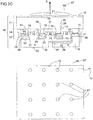
- FIGS. 2A to 2D show a total of four exemplary embodiments of an optoelectronic semiconductor body with different coupling-out structures according to the proposed principle.
- the in the FIGS. 2A to 2D Embodiments shown are a development of the in the Figures 1A and 1B illustrated embodiments.
- the semiconductor layer sequence 14, the first and the second electrical connection layers 15, 16, the first and the second insulator layer 23, 24, the mirror 27 and the transparent conductive oxide of FIG FIGS. 2A to 2D The embodiments shown correspond to the corresponding layers in FIG Figure 1A and 1B and are therefore not explained in detail below.
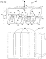
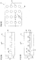
- the buffer layer 41 is deposited on the auxiliary carrier 40. In a photolithography and in an etching step, the buffer layer 41 is patterned to form the recesses 72. Subsequently, the epitaxial deposition of the semiconductor layer sequence 14 takes place.
- the thickness of the buffer layer 41 has a value from the interval between 0.5 ⁇ m and 8 ⁇ m. A typical value of the thickness of the buffer layer 41 is 3 ⁇ m.
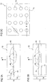
- FIG. 4C shows a cross section through the in FIG. 4A respectively FIG. 4B shown optoelectronic semiconductor body.
- FIG. 4C a cross-section through the buffer layer 41 is shown.
- the buffer layer 41 has circular recesses 72.
- a diameter D "of the recesses 72 has a value of an interval between 80 nm and 3 ⁇ m.
- a distance A "between two recesses has a value of an interval between 120 nm and 10 ⁇ m.
Landscapes
- Led Devices (AREA)
Applications Claiming Priority (3)
| Application Number | Priority Date | Filing Date | Title |
|---|---|---|---|
| DE102007049772 | 2007-09-28 | ||
| DE102008021403A DE102008021403A1 (de) | 2007-09-28 | 2008-04-29 | Optoelektronischer Halbleiterkörper und Verfahren zu dessen Herstellung |
| PCT/DE2008/001424 WO2009039812A1 (de) | 2007-09-28 | 2008-08-27 | Optoelektronischer halbleiterkörper |
Publications (2)
| Publication Number | Publication Date |
|---|---|
| EP2193555A1 EP2193555A1 (de) | 2010-06-09 |
| EP2193555B1 true EP2193555B1 (de) | 2016-07-06 |
Family
ID=40384515
Family Applications (1)
| Application Number | Title | Priority Date | Filing Date |
|---|---|---|---|
| EP08834030.2A Active EP2193555B1 (de) | 2007-09-28 | 2008-08-27 | Optoelektronischer halbleiterkörper |
Country Status (8)
| Country | Link |
|---|---|
| US (1) | US8362506B2 (https=) |
| EP (1) | EP2193555B1 (https=) |
| JP (1) | JP2010541216A (https=) |
| KR (1) | KR20100080819A (https=) |
| CN (1) | CN101796660B (https=) |
| DE (1) | DE102008021403A1 (https=) |
| TW (1) | TWI431802B (https=) |
| WO (1) | WO2009039812A1 (https=) |
Families Citing this family (20)
| Publication number | Priority date | Publication date | Assignee | Title |
|---|---|---|---|---|
| DE102007022947B4 (de) | 2007-04-26 | 2022-05-05 | OSRAM Opto Semiconductors Gesellschaft mit beschränkter Haftung | Optoelektronischer Halbleiterkörper und Verfahren zur Herstellung eines solchen |
| DE102008032318A1 (de) | 2008-03-31 | 2009-10-01 | Osram Opto Semiconductors Gmbh | Optoelektronischer Halbleiterchip und Verfahren zur Herstellung eines solchen |
| DE102008039790B4 (de) * | 2008-08-26 | 2022-05-12 | OSRAM Opto Semiconductors Gesellschaft mit beschränkter Haftung | Optoelektronisches Bauelement und Verfahren zu dessen Herstellung |
| DE102009019524B4 (de) * | 2009-04-30 | 2023-07-06 | OSRAM Opto Semiconductors Gesellschaft mit beschränkter Haftung | Optoelektronischer Halbleiterkörper mit einem reflektierenden Schichtsystem |
| TWI487141B (zh) * | 2009-07-15 | 2015-06-01 | 榮創能源科技股份有限公司 | 提高光萃取效率之半導體光電結構及其製造方法 |
| KR100999779B1 (ko) * | 2010-02-01 | 2010-12-08 | 엘지이노텍 주식회사 | 발광소자, 발광소자의 제조방법 및 발광소자 패키지 |
| KR101038923B1 (ko) * | 2010-02-02 | 2011-06-03 | 전북대학교산학협력단 | 개선된 발광 효율을 갖는 발광 다이오드 및 이의 제조방법 |
| KR101692410B1 (ko) * | 2010-07-26 | 2017-01-03 | 삼성전자 주식회사 | 발광소자 및 그 제조방법 |
| US9070851B2 (en) * | 2010-09-24 | 2015-06-30 | Seoul Semiconductor Co., Ltd. | Wafer-level light emitting diode package and method of fabricating the same |
| KR101154320B1 (ko) | 2010-12-20 | 2012-06-13 | 엘지이노텍 주식회사 | 발광소자, 발광소자 패키지 및 이를 포함하는 조명 장치 |
| DE102011114865B4 (de) | 2011-07-29 | 2023-03-02 | OSRAM Opto Semiconductors Gesellschaft mit beschränkter Haftung | Optoelektronisches Bauelement und Verfahren zur Herstellung eines optoelektronischen Bauelements |
| DE102012217533A1 (de) * | 2012-09-27 | 2014-03-27 | Osram Opto Semiconductors Gmbh | Verfahren zur Herstellung eines optoelektronischen Bauelements |
| JP6529223B2 (ja) * | 2014-06-30 | 2019-06-12 | 晶元光電股▲ふん▼有限公司Epistar Corporation | 光電部品 |
| DE102015104144A1 (de) * | 2015-03-19 | 2016-09-22 | Osram Opto Semiconductors Gmbh | Optoelektronischer Halbleiterkörper und Verfahren zur Herstellung eines optoelektronischen Halbleiterkörpers |
| CN108139035B (zh) | 2015-09-29 | 2020-07-10 | 昕诺飞控股有限公司 | 具有衍射耦出的光源 |
| FR3059788B1 (fr) * | 2016-12-02 | 2019-01-25 | Commissariat A L'energie Atomique Et Aux Energies Alternatives | Dispositif optoelectronique a diode electroluminescente a extraction augmentee |
| US11355549B2 (en) * | 2017-12-29 | 2022-06-07 | Lumileds Llc | High density interconnect for segmented LEDs |
| JP6843916B2 (ja) * | 2019-05-14 | 2021-03-17 | 晶元光電股▲ふん▼有限公司Epistar Corporation | 光電部品 |
| DE102019114315B4 (de) * | 2019-05-28 | 2025-04-17 | OSRAM Opto Semiconductors Gesellschaft mit beschränkter Haftung | Anordnung und verfahren zur herstellung einer anordnung |
| JP7223046B2 (ja) * | 2021-02-24 | 2023-02-15 | 晶元光電股▲ふん▼有限公司 | 光電部品 |
Family Cites Families (22)
| Publication number | Priority date | Publication date | Assignee | Title |
|---|---|---|---|---|
| US6031243A (en) * | 1996-10-16 | 2000-02-29 | Geoff W. Taylor | Grating coupled vertical cavity optoelectronic devices |
| JP4432180B2 (ja) | 1999-12-24 | 2010-03-17 | 豊田合成株式会社 | Iii族窒化物系化合物半導体の製造方法、iii族窒化物系化合物半導体素子及びiii族窒化物系化合物半導体 |
| US7053419B1 (en) | 2000-09-12 | 2006-05-30 | Lumileds Lighting U.S., Llc | Light emitting diodes with improved light extraction efficiency |
| US7064355B2 (en) | 2000-09-12 | 2006-06-20 | Lumileds Lighting U.S., Llc | Light emitting diodes with improved light extraction efficiency |
| US6791119B2 (en) * | 2001-02-01 | 2004-09-14 | Cree, Inc. | Light emitting diodes including modifications for light extraction |
| JP4055503B2 (ja) | 2001-07-24 | 2008-03-05 | 日亜化学工業株式会社 | 半導体発光素子 |
| TW558844B (en) | 2002-05-15 | 2003-10-21 | Opto Tech Corp | Light emitting diode capable of increasing light emitting brightness |
| JP2004241130A (ja) * | 2003-02-03 | 2004-08-26 | Seiko Epson Corp | 発光ディスプレイパネルおよびその製造方法 |
| US20050285128A1 (en) * | 2004-02-10 | 2005-12-29 | California Institute Of Technology | Surface plasmon light emitter structure and method of manufacture |
| KR100568297B1 (ko) * | 2004-03-30 | 2006-04-05 | 삼성전기주식회사 | 질화물 반도체 발광 소자 및 그 제조 방법 |
| TWI299914B (en) | 2004-07-12 | 2008-08-11 | Epistar Corp | Light emitting diode with transparent electrically conductive layer and omni directional reflector |
| KR100576870B1 (ko) | 2004-08-11 | 2006-05-10 | 삼성전기주식회사 | 질화물 반도체 발광소자 및 제조방법 |
| KR100624449B1 (ko) | 2004-12-08 | 2006-09-18 | 삼성전기주식회사 | 요철 구조를 포함하는 발광 소자 및 그 제조 방법 |
| KR100682872B1 (ko) | 2004-12-08 | 2007-02-15 | 삼성전기주식회사 | 고효율 반도체 발광 소자 및 그 제조방법 |
| KR100657941B1 (ko) | 2004-12-31 | 2006-12-14 | 삼성전기주식회사 | 요철 구조를 포함하는 발광 소자 및 그 제조 방법 |
| SG130975A1 (en) | 2005-09-29 | 2007-04-26 | Tinggi Tech Private Ltd | Fabrication of semiconductor devices for light emission |
| JP2007165726A (ja) * | 2005-12-15 | 2007-06-28 | Sony Corp | 半導体発光ダイオード |
| KR20070063731A (ko) | 2005-12-15 | 2007-06-20 | 엘지전자 주식회사 | 나노 패턴이 형성된 기판의 제조방법 및 그 기판을 이용한발광소자 |
| JP2007214276A (ja) * | 2006-02-08 | 2007-08-23 | Mitsubishi Chemicals Corp | 発光素子 |
| JP2007324579A (ja) * | 2006-05-01 | 2007-12-13 | Mitsubishi Chemicals Corp | 集積型半導体発光装置およびその製造方法 |
| WO2008144922A1 (en) * | 2007-06-01 | 2008-12-04 | Trojan Technologies | Ultraviolet radiation light emitting diode device |
| US7956370B2 (en) * | 2007-06-12 | 2011-06-07 | Siphoton, Inc. | Silicon based solid state lighting |
-
2008
- 2008-04-29 DE DE102008021403A patent/DE102008021403A1/de not_active Withdrawn
- 2008-08-27 KR KR1020107009324A patent/KR20100080819A/ko not_active Ceased
- 2008-08-27 JP JP2010526147A patent/JP2010541216A/ja active Pending
- 2008-08-27 CN CN200880106173.4A patent/CN101796660B/zh active Active
- 2008-08-27 US US12/678,259 patent/US8362506B2/en active Active
- 2008-08-27 WO PCT/DE2008/001424 patent/WO2009039812A1/de not_active Ceased
- 2008-08-27 EP EP08834030.2A patent/EP2193555B1/de active Active
- 2008-09-05 TW TW097134018A patent/TWI431802B/zh active
Also Published As
| Publication number | Publication date |
|---|---|
| US20100230698A1 (en) | 2010-09-16 |
| CN101796660A (zh) | 2010-08-04 |
| TWI431802B (zh) | 2014-03-21 |
| DE102008021403A1 (de) | 2009-04-02 |
| KR20100080819A (ko) | 2010-07-12 |
| JP2010541216A (ja) | 2010-12-24 |
| CN101796660B (zh) | 2012-05-30 |
| EP2193555A1 (de) | 2010-06-09 |
| US8362506B2 (en) | 2013-01-29 |
| TW200917537A (en) | 2009-04-16 |
| WO2009039812A1 (de) | 2009-04-02 |
Similar Documents
| Publication | Publication Date | Title |
|---|---|---|
| EP2193555B1 (de) | Optoelektronischer halbleiterkörper | |
| EP2150992B1 (de) | Halbleiterchip und verfahren zur herstellung eines halbleiterchips | |
| EP2015372B1 (de) | Halbleiterchip und Verfahren zur Herstellung eines Halbleiterchips | |
| DE102010034665B4 (de) | Optoelektronischer Halbleiterchip und Verfahren zur Herstellung von optoelektronischen Halbleiterchips | |
| EP2289115B1 (de) | Verfahren zur herstellung eines optoelektronischen bauelementes | |
| EP2248235B1 (de) | Kantenemittierender halbleiterlaser und verfahren zur herstellung eines kantenemittierenden halbleiterlasers | |
| EP2122697B1 (de) | Strahlung emittierender halbleiterkörper mit einer für die emittierte strahlung durchlässigen, elektrisch leitenden kontaktschicht | |
| EP2149159A1 (de) | Optoelektronischer halbleiterkörper und verfahren zur herstellung eines solchen | |
| DE102007019776A1 (de) | Optoelektronisches Bauelement und Verfahren zur Herstellung einer Mehrzahl optoelektronischer Bauelemente | |
| DE102007019775A1 (de) | Optoelektronisches Bauelement | |
| WO2007121739A2 (de) | Optoelektronisches halbleiterbauelement | |
| DE102006015788A1 (de) | Optoelektronischer Halbleiterchip | |
| EP2415086B1 (de) | Verfahren zur herstellung eines optoelektronischen bauelements, optoelektronisches bauelement und bauelementanordnung mit mehreren optoelektronischen bauelementen | |
| EP2057696B1 (de) | Optoelektronischer halbleiterchip und verfahren zur dessen herstellung | |
| DE102010032497A1 (de) | Strahlungsemittierender Halbleiterchip und Verfahren zur Herstellung eines strahlungsemittierenden Halbleiterchips | |
| DE102014111482B4 (de) | Verfahren zur Herstellung eines optoelektronischen Halbleiterchips | |
| DE10203809A1 (de) | Strahlungsemittierendes Halbleiterbauelement | |
| DE102017123154B4 (de) | Verfahren zur Herstellung eines optoelektronischen Bauelements und optoelektronisches Bauelement | |
| WO2017021301A1 (de) | Verfahren zur herstellung eines nitrid-halbleiterbauelements und nitrid-halbleiterbauelement | |
| DE102020106113A1 (de) | Strahlungsemittierender halbleiterkörper, strahlungsemittierender halbleiterchip und verfahren zur herstellung eines strahlungsemittierenden halbleiterkörpers | |
| WO2021032397A1 (de) | Optoelektronischer halbleiterchip | |
| WO2020156922A1 (de) | Optoelektronischer halbleiterchip und dessen herstellungsverfahren |
Legal Events
| Date | Code | Title | Description |
|---|---|---|---|
| PUAI | Public reference made under article 153(3) epc to a published international application that has entered the european phase |
Free format text: ORIGINAL CODE: 0009012 |
|
| 17P | Request for examination filed |
Effective date: 20100303 |
|
| AK | Designated contracting states |
Kind code of ref document: A1 Designated state(s): AT BE BG CH CY CZ DE DK EE ES FI FR GB GR HR HU IE IS IT LI LT LU LV MC MT NL NO PL PT RO SE SI SK TR |
|
| AX | Request for extension of the european patent |
Extension state: AL BA MK RS |
|
| DAX | Request for extension of the european patent (deleted) | ||
| REG | Reference to a national code |
Ref country code: DE Ref legal event code: R079 Ref document number: 502008014366 Country of ref document: DE Free format text: PREVIOUS MAIN CLASS: H01L0033000000 Ipc: H01L0033400000 |
|
| RIC1 | Information provided on ipc code assigned before grant |
Ipc: H01L 33/40 20100101AFI20151204BHEP Ipc: H01L 33/00 20100101ALI20151204BHEP Ipc: H01L 33/58 20100101ALI20151204BHEP |
|
| GRAP | Despatch of communication of intention to grant a patent |
Free format text: ORIGINAL CODE: EPIDOSNIGR1 |
|
| INTG | Intention to grant announced |
Effective date: 20160128 |
|
| GRAS | Grant fee paid |
Free format text: ORIGINAL CODE: EPIDOSNIGR3 |
|
| GRAA | (expected) grant |
Free format text: ORIGINAL CODE: 0009210 |
|
| AK | Designated contracting states |
Kind code of ref document: B1 Designated state(s): AT BE BG CH CY CZ DE DK EE ES FI FR GB GR HR HU IE IS IT LI LT LU LV MC MT NL NO PL PT RO SE SI SK TR |
|
| REG | Reference to a national code |
Ref country code: GB Ref legal event code: FG4D Free format text: NOT ENGLISH |
|
| REG | Reference to a national code |
Ref country code: AT Ref legal event code: REF Ref document number: 811254 Country of ref document: AT Kind code of ref document: T Effective date: 20160715 Ref country code: CH Ref legal event code: EP |
|
| REG | Reference to a national code |
Ref country code: IE Ref legal event code: FG4D Free format text: LANGUAGE OF EP DOCUMENT: GERMAN |
|
| REG | Reference to a national code |
Ref country code: DE Ref legal event code: R096 Ref document number: 502008014366 Country of ref document: DE |
|
| REG | Reference to a national code |
Ref country code: FR Ref legal event code: PLFP Year of fee payment: 9 |
|
| REG | Reference to a national code |
Ref country code: NL Ref legal event code: FP |
|
| REG | Reference to a national code |
Ref country code: LT Ref legal event code: MG4D |
|
| PG25 | Lapsed in a contracting state [announced via postgrant information from national office to epo] |
Ref country code: BE Free format text: LAPSE BECAUSE OF NON-PAYMENT OF DUE FEES Effective date: 20160831 |
|
| PG25 | Lapsed in a contracting state [announced via postgrant information from national office to epo] |
Ref country code: HR Free format text: LAPSE BECAUSE OF FAILURE TO SUBMIT A TRANSLATION OF THE DESCRIPTION OR TO PAY THE FEE WITHIN THE PRESCRIBED TIME-LIMIT Effective date: 20160706 Ref country code: NO Free format text: LAPSE BECAUSE OF FAILURE TO SUBMIT A TRANSLATION OF THE DESCRIPTION OR TO PAY THE FEE WITHIN THE PRESCRIBED TIME-LIMIT Effective date: 20161006 Ref country code: FI Free format text: LAPSE BECAUSE OF FAILURE TO SUBMIT A TRANSLATION OF THE DESCRIPTION OR TO PAY THE FEE WITHIN THE PRESCRIBED TIME-LIMIT Effective date: 20160706 Ref country code: LT Free format text: LAPSE BECAUSE OF FAILURE TO SUBMIT A TRANSLATION OF THE DESCRIPTION OR TO PAY THE FEE WITHIN THE PRESCRIBED TIME-LIMIT Effective date: 20160706 Ref country code: IS Free format text: LAPSE BECAUSE OF FAILURE TO SUBMIT A TRANSLATION OF THE DESCRIPTION OR TO PAY THE FEE WITHIN THE PRESCRIBED TIME-LIMIT Effective date: 20161106 |
|
| PG25 | Lapsed in a contracting state [announced via postgrant information from national office to epo] |
Ref country code: SE Free format text: LAPSE BECAUSE OF FAILURE TO SUBMIT A TRANSLATION OF THE DESCRIPTION OR TO PAY THE FEE WITHIN THE PRESCRIBED TIME-LIMIT Effective date: 20160706 Ref country code: PT Free format text: LAPSE BECAUSE OF FAILURE TO SUBMIT A TRANSLATION OF THE DESCRIPTION OR TO PAY THE FEE WITHIN THE PRESCRIBED TIME-LIMIT Effective date: 20161107 Ref country code: GR Free format text: LAPSE BECAUSE OF FAILURE TO SUBMIT A TRANSLATION OF THE DESCRIPTION OR TO PAY THE FEE WITHIN THE PRESCRIBED TIME-LIMIT Effective date: 20161007 Ref country code: ES Free format text: LAPSE BECAUSE OF FAILURE TO SUBMIT A TRANSLATION OF THE DESCRIPTION OR TO PAY THE FEE WITHIN THE PRESCRIBED TIME-LIMIT Effective date: 20160706 Ref country code: LV Free format text: LAPSE BECAUSE OF FAILURE TO SUBMIT A TRANSLATION OF THE DESCRIPTION OR TO PAY THE FEE WITHIN THE PRESCRIBED TIME-LIMIT Effective date: 20160706 Ref country code: PL Free format text: LAPSE BECAUSE OF FAILURE TO SUBMIT A TRANSLATION OF THE DESCRIPTION OR TO PAY THE FEE WITHIN THE PRESCRIBED TIME-LIMIT Effective date: 20160706 |
|
| REG | Reference to a national code |
Ref country code: CH Ref legal event code: PL |
|
| REG | Reference to a national code |
Ref country code: DE Ref legal event code: R097 Ref document number: 502008014366 Country of ref document: DE |
|
| PG25 | Lapsed in a contracting state [announced via postgrant information from national office to epo] |
Ref country code: MC Free format text: LAPSE BECAUSE OF FAILURE TO SUBMIT A TRANSLATION OF THE DESCRIPTION OR TO PAY THE FEE WITHIN THE PRESCRIBED TIME-LIMIT Effective date: 20160706 Ref country code: EE Free format text: LAPSE BECAUSE OF FAILURE TO SUBMIT A TRANSLATION OF THE DESCRIPTION OR TO PAY THE FEE WITHIN THE PRESCRIBED TIME-LIMIT Effective date: 20160706 Ref country code: LI Free format text: LAPSE BECAUSE OF NON-PAYMENT OF DUE FEES Effective date: 20160831 Ref country code: CH Free format text: LAPSE BECAUSE OF NON-PAYMENT OF DUE FEES Effective date: 20160831 Ref country code: RO Free format text: LAPSE BECAUSE OF FAILURE TO SUBMIT A TRANSLATION OF THE DESCRIPTION OR TO PAY THE FEE WITHIN THE PRESCRIBED TIME-LIMIT Effective date: 20160706 |
|
| PLBE | No opposition filed within time limit |
Free format text: ORIGINAL CODE: 0009261 |
|
| STAA | Information on the status of an ep patent application or granted ep patent |
Free format text: STATUS: NO OPPOSITION FILED WITHIN TIME LIMIT |
|
| PG25 | Lapsed in a contracting state [announced via postgrant information from national office to epo] |
Ref country code: SK Free format text: LAPSE BECAUSE OF FAILURE TO SUBMIT A TRANSLATION OF THE DESCRIPTION OR TO PAY THE FEE WITHIN THE PRESCRIBED TIME-LIMIT Effective date: 20160706 Ref country code: DK Free format text: LAPSE BECAUSE OF FAILURE TO SUBMIT A TRANSLATION OF THE DESCRIPTION OR TO PAY THE FEE WITHIN THE PRESCRIBED TIME-LIMIT Effective date: 20160706 Ref country code: BG Free format text: LAPSE BECAUSE OF FAILURE TO SUBMIT A TRANSLATION OF THE DESCRIPTION OR TO PAY THE FEE WITHIN THE PRESCRIBED TIME-LIMIT Effective date: 20161006 Ref country code: CZ Free format text: LAPSE BECAUSE OF FAILURE TO SUBMIT A TRANSLATION OF THE DESCRIPTION OR TO PAY THE FEE WITHIN THE PRESCRIBED TIME-LIMIT Effective date: 20160706 |
|
| REG | Reference to a national code |
Ref country code: IE Ref legal event code: MM4A |
|
| 26N | No opposition filed |
Effective date: 20170407 |
|
| GBPC | Gb: european patent ceased through non-payment of renewal fee |
Effective date: 20161006 |
|
| PG25 | Lapsed in a contracting state [announced via postgrant information from national office to epo] |
Ref country code: GB Free format text: LAPSE BECAUSE OF NON-PAYMENT OF DUE FEES Effective date: 20161006 Ref country code: IE Free format text: LAPSE BECAUSE OF NON-PAYMENT OF DUE FEES Effective date: 20160827 |
|
| REG | Reference to a national code |
Ref country code: FR Ref legal event code: PLFP Year of fee payment: 10 |
|
| PG25 | Lapsed in a contracting state [announced via postgrant information from national office to epo] |
Ref country code: LU Free format text: LAPSE BECAUSE OF NON-PAYMENT OF DUE FEES Effective date: 20160827 Ref country code: SI Free format text: LAPSE BECAUSE OF FAILURE TO SUBMIT A TRANSLATION OF THE DESCRIPTION OR TO PAY THE FEE WITHIN THE PRESCRIBED TIME-LIMIT Effective date: 20160706 |
|
| PG25 | Lapsed in a contracting state [announced via postgrant information from national office to epo] |
Ref country code: HU Free format text: LAPSE BECAUSE OF FAILURE TO SUBMIT A TRANSLATION OF THE DESCRIPTION OR TO PAY THE FEE WITHIN THE PRESCRIBED TIME-LIMIT; INVALID AB INITIO Effective date: 20080827 Ref country code: CY Free format text: LAPSE BECAUSE OF FAILURE TO SUBMIT A TRANSLATION OF THE DESCRIPTION OR TO PAY THE FEE WITHIN THE PRESCRIBED TIME-LIMIT Effective date: 20160706 |
|
| PG25 | Lapsed in a contracting state [announced via postgrant information from national office to epo] |
Ref country code: MT Free format text: LAPSE BECAUSE OF FAILURE TO SUBMIT A TRANSLATION OF THE DESCRIPTION OR TO PAY THE FEE WITHIN THE PRESCRIBED TIME-LIMIT Effective date: 20160706 Ref country code: TR Free format text: LAPSE BECAUSE OF FAILURE TO SUBMIT A TRANSLATION OF THE DESCRIPTION OR TO PAY THE FEE WITHIN THE PRESCRIBED TIME-LIMIT Effective date: 20160706 |
|
| REG | Reference to a national code |
Ref country code: FR Ref legal event code: PLFP Year of fee payment: 11 |
|
| P01 | Opt-out of the competence of the unified patent court (upc) registered |
Effective date: 20230825 |
|
| REG | Reference to a national code |
Ref country code: DE Ref legal event code: R079 Ref document number: 502008014366 Country of ref document: DE Free format text: PREVIOUS MAIN CLASS: H01L0033400000 Ipc: H10H0020832000 |
|
| PGFP | Annual fee paid to national office [announced via postgrant information from national office to epo] |
Ref country code: NL Payment date: 20250821 Year of fee payment: 18 |
|
| PGFP | Annual fee paid to national office [announced via postgrant information from national office to epo] |
Ref country code: DE Payment date: 20250820 Year of fee payment: 18 |
|
| PGFP | Annual fee paid to national office [announced via postgrant information from national office to epo] |
Ref country code: IT Payment date: 20250825 Year of fee payment: 18 |
|
| PGFP | Annual fee paid to national office [announced via postgrant information from national office to epo] |
Ref country code: FR Payment date: 20250829 Year of fee payment: 18 Ref country code: AT Payment date: 20250821 Year of fee payment: 18 |