EP2192610A2 - Bearbeitungsverfahren zum Vereinheitlichen der Schichtdickenverteilung einer Schicht mit vorher festgelegter Schichtdicke, die auf einer Oberfläche eines Siliziumwafers ausgebildet ist, und Verarbeitungsverfahren zum Vereinheitlichen der Dickenverteilung eines Siliziumwafers - Google Patents
Bearbeitungsverfahren zum Vereinheitlichen der Schichtdickenverteilung einer Schicht mit vorher festgelegter Schichtdicke, die auf einer Oberfläche eines Siliziumwafers ausgebildet ist, und Verarbeitungsverfahren zum Vereinheitlichen der Dickenverteilung eines Siliziumwafers Download PDFInfo
- Publication number
- EP2192610A2 EP2192610A2 EP09176717A EP09176717A EP2192610A2 EP 2192610 A2 EP2192610 A2 EP 2192610A2 EP 09176717 A EP09176717 A EP 09176717A EP 09176717 A EP09176717 A EP 09176717A EP 2192610 A2 EP2192610 A2 EP 2192610A2
- Authority
- EP
- European Patent Office
- Prior art keywords
- film thickness
- layer
- etching
- silicon wafer
- natural oxide
- Prior art date
- Legal status (The legal status is an assumption and is not a legal conclusion. Google has not performed a legal analysis and makes no representation as to the accuracy of the status listed.)
- Withdrawn
Links
Images



Classifications
-
- H—ELECTRICITY
- H10—SEMICONDUCTOR DEVICES; ELECTRIC SOLID-STATE DEVICES NOT OTHERWISE PROVIDED FOR
- H10P—GENERIC PROCESSES OR APPARATUS FOR THE MANUFACTURE OR TREATMENT OF DEVICES COVERED BY CLASS H10
- H10P50/00—Etching of wafers, substrates or parts of devices
- H10P50/60—Wet etching
- H10P50/64—Wet etching of semiconductor materials
- H10P50/642—Chemical etching
Definitions
- the present invention relates to a processing method for uniformizing a film thickness distribution of a layer (e.g., an SOI layer of an SOI wafer) having predetermined film thickness formed on the surface of a silicon wafer and a processing method for uniformizing a thickness distribution of a silicon wafer.
- a layer e.g., an SOI layer of an SOI wafer
- Layers having predetermined film thickness such as an SOI (Silicon On Insulator) layer, a surface silicon layer formed by DSB (Direct Silicon Bonding), an epitaxial layer, and a polysilicon layer are formed on the surface of a silicon wafer according to applications.
- SOI Silicon On Insulator
- DSB Direct Silicon Bonding
- the SOI layer is formed on a main surface of a SIMOX wafer, in which a buried oxide layer (BOX: Buried OXide) is formed in the silicon wafer, by, for example, a SIMOX (Separation by IMplanted OXygen) method.
- BOX Buried OXide
- a DSB wafer formed by directly bonding two silicon wafers without the intervention of a BOX layer is also performed.
- the DSB wafer is formed by directly bonding a silicon wafer for active layer and a silicon wafer for support, which have different crystal orientations, after SC1-cleaning the same.
- the surface silicon layer is formed by performing grinding or the like from the surface of the silicon wafer for active layer.
- the thickness of the SOI layer of the SIMOX wafer affects a manufacturing process for a semiconductor device and the like and a characteristic of the semiconductor device. Therefore, as described in, for example, JP2007-266059A , after an oxide film on the SOI layer is removed, the layer thickness of the SOI layer is measured and, when the layer thickness exceeds a predetermined layer thickness, the SOI layer is removed by etching to adjust the layer thickness.
- the SOI layer is only etched substantially uniformly or with a fixed distribution. Uniformity of the film thickness of the SOI layer is not taken into account.
- a thick film portion in which the film thickness of the SOI layer is large and a thin film portion in which the film thickness is small occur because of, for example, variation in a treatment gas flow rate and a temperature distribution during heat treatment and the like.
- a non-uniform distribution of the thick film portion and the thin film portion having such film thicknesses is small (e.g., several angstroms to several tens angstroms).
- a semiconductor device is formed by using the SIMOX wafer in which the film thickness of the SOI layer is non-uniform, there is a fear that a characteristic of the semiconductor device is adversely affected and yield falls. Therefore, it is desired to uniformize a film thickness distribution of the SOI layer.
- the SOI layer it is also desired to uniformize a film thickness distribution of the layers having the predetermined film thicknesses formed on the surface of the silicon wafer such as the surface silicon layer formed by the DSB, the epitaxial layer, and the polysilicon layer. Further, it is also desired to uniformize a thickness distribution of the silicon wafer itself.
- a first problem to be solved by the present invention is to uniformize a film thickness distribution of a layer having predetermined film thickness formed on the surface of a silicon wafer.
- a second problem to be solved by the present invention is to uniformize a thickness distribution of the silicon wafer.
- a first aspect of the present invention is a processing method for uniformizing a film thickness distribution of a layer having predetermined film thickness formed on the surface of a silicon wafer, the processing method characterized by including an oxidation step of forming a natural oxide film on the surface of the layer having the predetermined film thickness; and an etching step of removing, with etching liquid, the natural oxide film formed in a local thick film portion of the layer having the predetermined film thickness while leaving a part of the thickness.
- the layer having the predetermined film thickness formed on the surface of the silicon wafer is any one of an SOI layer on a main surface of an SOI wafer in which a buried oxide layer is formed, a surface silicon layer formed by the DSB, an epitaxial layer, and a polysilicon layer.
- etching liquid e.g., a mixed solution of hydrofluoric acid (HF) and ozone water
- the SOI surface is exposed and tends to absorb foreign matters such as particles because the exposed SOI surface has water repellency. If the absorbed particles cannot be fully removed in a cleaning step after that, a characteristic of a semiconductor device is affected.
- the present invention has been devised in view of the fact that the thickness of the natural oxide film formed on the surface of the SOI layer depends upon a diffusion characteristic of oxygen diffusing in the SOI layer and is fixed thickness irrespective of a film thickness distribution of the SOI layer. Specifically, it is possible to reduce the thickness of the thick film portion and uniformize the film thickness of the SOI layer by locally removing, with the etching liquid, only the natural oxide film of the SOI layer formed in the thick film portion of the SOI layer. In this case, it is essential to remove, with the etching liquid, the natural oxide film formed on the main surface of the SOI layer while leaving a part (e.g., 1 ⁇ to 2 ⁇ ) of the thickness of the natural oxide film. Consequently, since the SOI surface is not exposed, it is possible to prevent the particles of the foreign matters from adhering to the SOI surface.
- the thickness of the natural oxide film it is preferable to set an upper limit for the thickness of the natural oxide film to be removed by one etching and prevent the SOI surface from being exposed. In this case, it is desirable to repeatedly perform the oxidation step and the etching step according to the thickness of the thick film portion of the SOI layer.
- the natural oxide film can be formed by applying the ozone water to the main surface of the SOI layer. In this case, it is preferable to clean residual ozone components on the main surface with pure water after forming the natural oxide film. Further, it is desirable to use hydrofluoric acid as the etching liquid. Specifically, since the SOI layer cannot be etched by the hydrofluoric acid, the natural oxide film is once formed on the main surface of the SOI layer of the thick film portion and only the portion of the natural oxide film of the thick film portion is etched to uniformize the film thickness of the SOI layer.
- a second aspect of the processing method for uniformizing a film thickness distribution of a layer having predetermined film thickness formed on the surface of a silicon wafer is characterized by including: a measuring step of measuring a film thickness distribution of the layer having the predetermined film thickness formed on the surface of the silicon wafer; a film thickness adjustment region setting step of setting, on the basis of the film thickness distribution of the layer having the predetermined film thickness measured by the measuring step, a thick film portion that should be etched; a target etching amount setting step of setting a target etching amount of a set film thickness adjustment region; an oxidation step of forming a natural oxide film on the surface of the layer having the predetermined film thickness; and an etching step of removing, with etching liquid, the natural oxide film formed in the thick film portion that should be etched while leaving a part of the thickness of the natural oxide film.
- the layer having the predetermined film thickness formed on the surface of the silicon wafer is any one of an SOI layer on a main surface of an SOI wafer in which a buried oxide layer is formed, a surface silicon layer formed by the DSB, an epitaxial layer, and a polysilicon layer.
- a film thickness distribution of the SOI layer on the main surface of the SOI wafer is measured and a film thickness adjustment region of the thick film portion that should be removed by etching is set on the basis of the measured film thickness distribution of the SOI layer.
- This film thickness adjustment region can be set in plural places according to the film thickness distribution. It is preferable to set a center point of the film thickness adjustment region taking into account the spread of the etching liquid on the main surface of the SOI layer. A target etching amount of the set film thickness adjustment region is set.
- a target etching amount is set on the basis of a measurement value of the film thickness distribution and according to the thicknesses of thick film portions of respective film thickness adjustment regions with reference to the thinnest film portion.
- an upper limit for the thickness of the natural oxide film it is preferable to set an upper limit for the thickness of the natural oxide film to be removed by one etching for center points of the respective film thickness adjustment regions and prevent the SOI surface from being exposed.
- the oxidation step can include a step of applying ozone water to the main surface to form the natural oxide film and a step of cleaning, with pure water, residual ozone components on the main surface after this step.
- the etching step it is possible to use an etching nozzle including an etching liquid nozzle that causes any one of solutions of hydrofluoric acid, buffered hydrofluoric acid, and fluoric ammonium to flow out as the etching liquid and plural pure water nozzles that are arranged to surround this etching liquid nozzle and cause the pure water to flow out.
- the etching step is performed with the etching nozzle moved to and positioned in the center points of the respective film thickness adjustment regions in a state in which the SOI wafer is fixed.
- the etching nozzle according to the present invention since the plural pure water nozzles are circularly arranged to surround the etching liquid nozzle, it is possible to suppress the spread of the etching liquid with the pure water and limit an etching region. Note that an etching amount has fixed spread from the center of the etching liquid nozzle and a distribution occurs in which the etching amount decreases farther away from the center. Therefore, it is preferable to set the center points of the respective film thickness adjustment regions taking into account the distribution of the etching amount.
- a processing method for uniformizing a thickness distribution of a silicon wafer of the present invention is characterized by including: an oxidation step of forming a natural oxide film on a main surface of the silicon wafer; and an etching step of removing, with etching liquid, the natural oxide film formed in a locally thick portion of the silicon wafer while leaving a part of the thickness of the natural oxide film.
- a processing method for uniformizing a film thickness distribution of a layer having predetermined film thickness formed on the surface of a silicon wafer according to the present invention is explained below on the basis of an embodiment. This embodiment is explained with reference to an SOI layer on an SOI wafer main surface as an example of the layer having the predetermined film thickness formed on the surface of the silicon wafer.
- FIG. 1 A procedure in an embodiment of the processing method for uniformizing a film thickness distribution of an SOI layer as an SOI wafer main surface is shown in FIG. 1 .
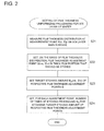
- a setting procedure in the embodiment of uniformizing processing for a film thickness distribution of an SOI layer is shown in FIG. 2 .
- FIG. 3 A schematic diagram of a uniformizing processing apparatus for explaining operation in the embodiment is shown in FIG. 3 .
- FIG. 4 A schematic diagram of an etching nozzle in the embodiment is shown in FIG. 4 .
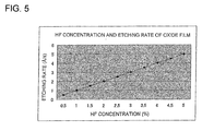
- FIG. 5 A graph of a relation between the concentration of hydrofluoric acid and an etching rate of an oxide film is shown in FIG. 5 .
- a film thickness distribution of a main surface of the SOI layer is measured.
- plural measurement points P(ri, ⁇ j) are set on a main surface of a circular SOI wafer according to, for example, a polar coordinate system (r, ⁇ ).
- ri is a radius position.
- ⁇ j is a rotation angle (0 ⁇ to 2 ⁇ ) from a reference position (e.g., a notch) of the SOI wafer.
- i and j are natural numbers.
- Film thicknesses at the respective measurement points P(ri, ⁇ j) can be measured by using, for example, an optical measuring device that analyzes interference of reflection of light and measures film thickness.
- the measurement of film thicknesses is not limited to this.
- a center point Q(rm, ⁇ n) of a film thickness adjustment region is set in a thick film portion, which should be removed by etching, on the basis of the film thickness distribution of the SOI layer measured in step S21.
- a plurality of the center points Q of the film thickness adjustment region can be set according to the film thickness distribution. As explained later, the center point Q of the film thickness adjustment region is set with the spread of etching liquid flowing out to the main surface of the SOI layer taken into account.
- a target etching amount E Q (rm, ⁇ n) is set concerning the center points Q of the respective film thickness adjustment regions set in step S22.
- This target etching amount E Q is set on the basis of a measurement value of the film thickness distribution and according to the thickness of thick film portions of the respective film thickness adjustment regions with reference to the thinnest film portion.
- a number of times of etching processing N (a natural number) that attains the target etching amount E Q of the center points Q of the respective film thickness adjustment regions set in step S23 is set.
- the thickness of the natural oxide film formed on the main surface of the SOI layer by causing ozone water to flow out depends upon a diffusion characteristic of oxygen to the SOI layer and depends upon processing time by the ozone water.
- an upper limit value e.g., 6 ⁇
- the target etching amount E Q cannot be attained by one etching. Therefore, the number of times of etching processing N necessary for attaining the target etching amount E Q is set.
- steps S21 to S24 a film thickness distribution on the SOI layer main surface is measured for each one SOI wafer and the target etching amount E Q of the center point Q of the film thickness adjustment region set on the basis of the thick film portion requiring thickness adjustment and the number of times of etching processing N (a natural number) necessary for attaining the target etching amount E Q are set.
- the film thickness of the SOI layer of the SOI wafer is subjected to uniformizing processing according to the procedure shown in FIG. 1 on the basis of the center points Q of the respective film thickness adjustment regions set for each one SOI wafer, the target etching amount E Q of the center points of the respective film thickness adjustment regions set, and the number of times of etching processing N Q set for each of the film thickness adjustment regions in steps S21 to S24 in FIG. 2 .
- the uniformizing processing for the SOI layer film thickness of the SOI wafer main surface can be executed by using, for example, the uniformizing processing apparatus shown in the schematic diagram in FIG. 3 .
- each SOI wafer 1 as a processing target is fixed on an upper surface of a not-shown turntable by plural (in the example shown in the figure, four) clamps 2.
- the turntable controllably holds a rotation angle with a spin chuck having high corrosion resistance.
- a notch 3 indicating a reference position is fixed according to the position of the turntable set in advance.
- An ozone water nozzle 4 and a pure water nozzle 5 are arranged above a main surface of the SOI wafer 1.
- An etching nozzle 6 is arranged above the main surface of the SOI wafer 1 and held to be movable in a radial direction of the main surface of the SOI wafer 1.
- the etching nozzle 6 is configured by arranging, for example, as shown in FIG. 4 , one hydrofluoric acid nozzle 7 that causes hydrofluoric acid to flow out and plural (in the example shown in the figure, six) pure water nozzles 8 along a circle around the hydrofluoric acid nozzle 7.
- a diameter D of a circle 9 in which the pure water nozzles 8 are arranged can be set to about 25 mm to 50 mm.
- a diameter D of the etching nozzle 6 can be set as appropriate with target accuracy and processing time of film thickness uniformity taken into account. Specifically, since the size of the diameter D corresponds to the size of an area to be etched with hydrofluoric acid, when target accuracy of planarization is set high, it is desirable to set the size of the diameter D small. However, since the number of center points of the film thickness adjustment regions increases, the processing time increases.
- the SOI wafer 1 is mounted on the turntable with the position (a rotation angle position) of the notch 3 of the SOI wafer 1 set in the reference position.
- the ozone water is caused to flow out to the main surface of the SOI layer from the ozone water nozzle 4 while the turntable is rotated to rotate the SOI wafer 1. Consequently, the ozone water is applied to the main surface of the SOI layer, oxygen ion in the ozone water diffuses to the inside of the SOI layer, and a natural oxide film having uniform thickness is formed over the entire main surface.
- the thickness of the natural oxide film can be managed according to, for example, application time of the ozone water.
- step S12 After the natural oxide film having predetermined thickness (e.g., 6 ⁇ ) is formed in step S12, ozone components on the main surface of the SOI layer are cleaned (rinsed) by the pure water to stop the oxidation while the SOI wafer 1 is rotated.
- predetermined thickness e.g. 6 ⁇
- the etching nozzle 6 is aligned with the center point Q (rm, ⁇ n) of the film thickness adjustment region.
- the position of the etching nozzle 6 is moved to a circumferential edge of the SOI wafer 1.
- An angle position of the SOI wafer 1 is set such that the center point Q(rm, ⁇ n) of the film thickness adjustment region is set in an angle position in a moving direction of the etching nozzle 6.
- the etching nozzle 6 is moved in the radial direction toward the center of the SOI wafer 1 and stopped at the center point Q(rm, ⁇ n) of predetermined film thickness adjustment region.
- the pure water is caused to continuously flow out from the pure water nozzles 8 to prevent the hydrofluoric acid from spreading from the set center point Q(rm, ⁇ n) of the film thickness adjustment region.
- the etching is prevented from spreading to regions other than the center point of the film thickness adjustment region. Since a distribution occurs in which an etching amount decreases farther away from the center of the hydrofluoric acid nozzle 7, in step S22 in FIG. 2 , the center point of the film thickness adjustment region is set with the distribution of the etching amount taken into account.
- N Q times of etching processing set for each of the center points Q of the respective film thickness adjustment regions ends. If there is a film thickness adjustment region where the etching processing has not reached N Q times yet, the procedure returns to S12 and is repeated. When the etching processing set for all the film thickness adjustment regions ends N Q times, the procedure shifts to step S18.
- the ozone water is caused to flow out from the ozone water nozzle 4 to the SOI layer main surface of the SOI wafer 1 while the SOI wafer 1 is rotated. Consequently, a natural oxide film having uniform thickness is formed over the entire main surface of the SOI wafer 1.
- the pure water is caused to flow out from the pure water nozzle 5 to the SOI layer main surface of the SOI wafer 1 to clean (rinse) ozone components on the main surface while the SOI wafer 1 is rotated.
- the ozone concentration of the ozone water used for the generation of the natural oxide film can be set to 200 ppm. However, the ozone concentration is selected in a range of 5 ppm to 100 ppm.
- the concentration of the hydrofluoric acid can be set to 1%. However, the concentration is selected in a range of 0.25% to 5%.
- the number of measurement points of an irregularity distribution on the main surface can be set to fifty-seven in, for example, an SOI wafer having a 300 mm diameter. However, the number of measurement points only has to be set according to a relation with target accuracy of planarization.
- a procedure of the planarization processing can be established by forming an irregularity pattern at, for example, a 3 ⁇ unit and setting the number of times of etching processing N to, for example, "3" on the basis of an initial irregularity distribution on the main surface of the SOI wafer.
- an etching amount of the natural oxide film by hydrofluoric acid (HF) is related to an etching rate ( ⁇ /second) that depends upon the concentration (%) and the temperature of the hydrofluoric acid. Therefore, the concentration (%) and an amount (flow-out time) of the hydrofluoric acid caused to flow out from the hydrofluoric acid nozzle 7 are controlled according to a target etching amount per one time.
- the temperature of the hydrofluoric acid is 20°C to 30°C.
- FIG. 6 A graph of a relation between the concentration of the hydrofluoric acid and the etching rate of the natural oxide film is shown in FIG. 6 .
- a first column represents the concentration (%) of the hydrofluoric acid
- a second column represents the etching rate ( ⁇ /s) of the oxide film
- a third column represents processing time in etching the oxide film by 5 ⁇ .
- An etching amount can be managed according to time on the basis of these hydrofluoric acid concentrations (%) and etching processing time.
- the ozone water is applied to the main surface of the SOI layer and converted into the natural oxide film. Therefore, the natural oxide film can be easily etched with the hydrofluoric acid and the etching processing can be locally performed. Therefore, a film thickness distribution of the SOI layer can be accurately uniformized by repeating these kinds of processing to subject the thick film portion of the SOI layer to the etching processing.
- the natural oxide film of the SOI layer is etched with the hydrofluoric acid such that the SOI surface is not exposed with a part (e.g., 1 to 2 ⁇ ) of the thickness of the natural oxide film of the SOI layer left, i.e., with the upper limit set for the thickness of the natural oxide film to be removed by one etching. Therefore, particles of foreign matters can be prevented from adhering to the SOI surface and yield and the like of the semiconductor device can be improved.
- the hydrofluoric acid caused to flow out from the hydrofluoric acid nozzle 7 is prevented from spreading from the film thickness adjustment region by causing the pure water to continuously flow out from the pure water nozzles 8. Therefore, since an area to be etched for film thickness adjustment can be accurately controlled, uniformity of film thickness can be accurately adjusted.
- uniformizing of the film thickness distribution of the SOI layer on the SOI wafer main surface is explained as the example.
- the present invention is not limited to this.
- a film thickness distribution of any one of a surface silicon layer formed by the DSB, an epitaxial layer, and a polysilicon layer can also be uniformized.
- an SOI layer and layers having predetermined film thickness such as a surface silicon layer formed by the DSB, an epitaxial layer, and a polysilicon layer are formed on the surface of a silicon wafer according to applications.
- a film thickness distribution can be uniformized according to a principle the same as a principle for uniformizing the film thickness distribution of the SOI layer explained above.
- the present invention can be applied not only to a case in which a film thickness distribution of a layer having predetermined film thickness formed on the surface of a silicon wafer is uniformized but also to a case in which a thickness distribution of the silicon wafer itself is uniformized.
- the thickness of a natural oxide film formed on the surface of the silicon wafer depends upon a diffusion characteristic of oxygen diffusing to the silicon wafer and is fixed thickness irrespective of the thickness distribution of the silicon wafer. Therefore, the thickness distribution of the silicon wafer can be uniformized according to the principle same as the principle for uniformizing of the film thickness distribution of the SOI layer.
- the processing method for uniformizing a thickness distribution of a silicon wafer is configured by including an oxidation step of forming a natural oxide film on a main surface of the silicon wafer and an etching step of removing, with etching liquid, the natural oxide film formed in a locally thick portion of the silicon wafer while leaving a part of the thickness of the natural oxide film.
- the oxidation step and the etching step are repeatedly performed according to the thickness of the locally thick portion of the silicon wafer.
Landscapes
- Weting (AREA)
- Element Separation (AREA)
Applications Claiming Priority (1)
| Application Number | Priority Date | Filing Date | Title |
|---|---|---|---|
| JP2008301258 | 2008-11-26 |
Publications (1)
| Publication Number | Publication Date |
|---|---|
| EP2192610A2 true EP2192610A2 (de) | 2010-06-02 |
Family
ID=41822546
Family Applications (1)
| Application Number | Title | Priority Date | Filing Date |
|---|---|---|---|
| EP09176717A Withdrawn EP2192610A2 (de) | 2008-11-26 | 2009-11-23 | Bearbeitungsverfahren zum Vereinheitlichen der Schichtdickenverteilung einer Schicht mit vorher festgelegter Schichtdicke, die auf einer Oberfläche eines Siliziumwafers ausgebildet ist, und Verarbeitungsverfahren zum Vereinheitlichen der Dickenverteilung eines Siliziumwafers |
Country Status (3)
| Country | Link |
|---|---|
| US (1) | US20100129941A1 (de) |
| EP (1) | EP2192610A2 (de) |
| JP (1) | JP2010153809A (de) |
Cited By (3)
| Publication number | Priority date | Publication date | Assignee | Title |
|---|---|---|---|---|
| EP3644346A4 (de) * | 2017-06-23 | 2021-03-17 | Shin-Etsu Handotai Co., Ltd. | Verfahren zur herstellung eines soi-wafers |
| FR3104810A1 (fr) * | 2019-12-17 | 2021-06-18 | Soitec | Procede de gravure de substrats comportant une couche mince superficielle, pour ameliorer l’uniformite d’epaisseur de ladite couche |
| FR3155359A1 (fr) * | 2023-11-14 | 2025-05-16 | Soitec | Procede d’amincissement de la couche superficielle d’un substrat soi |
Families Citing this family (6)
| Publication number | Priority date | Publication date | Assignee | Title |
|---|---|---|---|---|
| CN103560076B (zh) * | 2013-11-12 | 2016-01-06 | 深圳市华星光电技术有限公司 | 提升多晶硅层均一性的多晶硅制作方法 |
| JP6086105B2 (ja) * | 2014-09-24 | 2017-03-01 | 信越半導体株式会社 | Soiウェーハの製造方法 |
| US11179694B2 (en) * | 2017-09-11 | 2021-11-23 | Basf Se | Method of forming porous metal oxide microspheres |
| CN113496891B (zh) * | 2020-04-03 | 2023-03-14 | 重庆超硅半导体有限公司 | 一种集成电路硅片表面氧化膜自适应均匀腐蚀方法 |
| JP7574841B2 (ja) * | 2022-11-15 | 2024-10-29 | 株式会社Sumco | シリコンウェーハの洗浄方法、シリコンウェーハの製造方法、及びシリコンウェーハ |
| JP7790685B1 (ja) * | 2025-08-25 | 2025-12-23 | SHW Tech株式会社 | 半導体製造装置及び半導体製造方法 |
Citations (1)
| Publication number | Priority date | Publication date | Assignee | Title |
|---|---|---|---|---|
| JP2007266059A (ja) | 2006-03-27 | 2007-10-11 | Sumco Corp | Simoxウェーハの製造方法 |
Family Cites Families (11)
| Publication number | Priority date | Publication date | Assignee | Title |
|---|---|---|---|---|
| JP3154814B2 (ja) * | 1991-06-28 | 2001-04-09 | 株式会社東芝 | 半導体ウエハの洗浄方法および洗浄装置 |
| JP3341033B2 (ja) * | 1993-06-22 | 2002-11-05 | 忠弘 大見 | 回転薬液洗浄方法及び洗浄装置 |
| US7378355B2 (en) * | 1997-05-09 | 2008-05-27 | Semitool, Inc. | System and methods for polishing a wafer |
| US7416611B2 (en) * | 1997-05-09 | 2008-08-26 | Semitool, Inc. | Process and apparatus for treating a workpiece with gases |
| JP3324469B2 (ja) * | 1997-09-26 | 2002-09-17 | 信越半導体株式会社 | Soiウエーハの製造方法ならびにこの方法で製造されるsoiウエーハ |
| JP4339561B2 (ja) * | 2002-08-16 | 2009-10-07 | 大日本スクリーン製造株式会社 | 基板処理装置および基板処理方法 |
| US6764883B1 (en) * | 2003-01-07 | 2004-07-20 | International Business Machines Corp. | Amorphous and polycrystalline silicon nanolaminate |
| US7431040B2 (en) * | 2003-09-30 | 2008-10-07 | Tokyo Electron Limited | Method and apparatus for dispensing a rinse solution on a substrate |
| JP4977999B2 (ja) * | 2005-11-21 | 2012-07-18 | 株式会社Sumco | 貼合せ基板の製造方法及びその方法で製造された貼合せ基板 |
| KR100811267B1 (ko) * | 2005-12-22 | 2008-03-07 | 주식회사 하이닉스반도체 | 반도체소자의 듀얼게이트 형성방법 |
| JP2010040593A (ja) * | 2008-07-31 | 2010-02-18 | Sumco Corp | イオン注入装置及び方法 |
-
2009
- 2009-11-09 JP JP2009256502A patent/JP2010153809A/ja active Pending
- 2009-11-10 US US12/615,353 patent/US20100129941A1/en not_active Abandoned
- 2009-11-23 EP EP09176717A patent/EP2192610A2/de not_active Withdrawn
Patent Citations (1)
| Publication number | Priority date | Publication date | Assignee | Title |
|---|---|---|---|---|
| JP2007266059A (ja) | 2006-03-27 | 2007-10-11 | Sumco Corp | Simoxウェーハの製造方法 |
Cited By (7)
| Publication number | Priority date | Publication date | Assignee | Title |
|---|---|---|---|---|
| EP3644346A4 (de) * | 2017-06-23 | 2021-03-17 | Shin-Etsu Handotai Co., Ltd. | Verfahren zur herstellung eines soi-wafers |
| US11244851B2 (en) | 2017-06-23 | 2022-02-08 | Shin-Etsu Handotai Co., Ltd. | Method for manufacturing SOI wafer |
| FR3104810A1 (fr) * | 2019-12-17 | 2021-06-18 | Soitec | Procede de gravure de substrats comportant une couche mince superficielle, pour ameliorer l’uniformite d’epaisseur de ladite couche |
| WO2021123529A1 (fr) * | 2019-12-17 | 2021-06-24 | Soitec | Procede de gravure de substrats comportant une couche mince superficielle, pour ameliorer l'uniformite d'epaisseur de ladite couche |
| US12040194B2 (en) | 2019-12-17 | 2024-07-16 | Soitec | Method for etching substrates comprising a thin surface layer, for improving the uniformity of thickness of the layer |
| FR3155359A1 (fr) * | 2023-11-14 | 2025-05-16 | Soitec | Procede d’amincissement de la couche superficielle d’un substrat soi |
| WO2025103687A1 (fr) * | 2023-11-14 | 2025-05-22 | Soitec | Procede d'amincissement de la couche superficielle d'un substrat soi |
Also Published As
| Publication number | Publication date |
|---|---|
| US20100129941A1 (en) | 2010-05-27 |
| JP2010153809A (ja) | 2010-07-08 |
Similar Documents
| Publication | Publication Date | Title |
|---|---|---|
| EP2192610A2 (de) | Bearbeitungsverfahren zum Vereinheitlichen der Schichtdickenverteilung einer Schicht mit vorher festgelegter Schichtdicke, die auf einer Oberfläche eines Siliziumwafers ausgebildet ist, und Verarbeitungsverfahren zum Vereinheitlichen der Dickenverteilung eines Siliziumwafers | |
| CN105531811B (zh) | 衬底背面纹理 | |
| US20070275562A1 (en) | Apparatus and method for treating substrate, and injection head used in the apparatus | |
| US10403518B2 (en) | Substrate processing method, substrate processing apparatus and recording medium | |
| KR102259162B1 (ko) | Soi 웨이퍼의 제조방법 | |
| CN108140556B (zh) | 基片背侧纹理化 | |
| KR20180112063A (ko) | 선택적 SiARC 제거 | |
| CN114649233B (zh) | 晶圆清洗装置及清洗晶圆的方法 | |
| US20180277379A1 (en) | Liquid mixture and method for selectively wet etching silicon germanium | |
| EP4418307A1 (de) | Substratverarbeitungsverfahren und substratverarbeitungssystem | |
| KR20210074999A (ko) | 반도체 웨이퍼 다이싱 공정 | |
| CN110071055B (zh) | 基板处理装置及基板处理方法 | |
| CN110571166B (zh) | 晶边刻蚀方法和半导体器件制造方法 | |
| KR101099733B1 (ko) | 기판 처리 장치 | |
| JP2015119128A (ja) | 基板処理装置および基板処理方法 | |
| JPWO2023026909A5 (ja) | 基板処理方法及び基板処理システム | |
| JPWO2022270129A5 (de) | ||
| TW202109617A (zh) | 形成光阻層的裝置、形成遮罩層的方法與形成光阻層的方法 | |
| CN114830302B (zh) | 蚀刻包括薄表面层的基板以改善所述层的厚度均匀性的方法 | |
| KR101198356B1 (ko) | 확산 웨이퍼의 제조방법 및 확산 웨이퍼 | |
| KR100706781B1 (ko) | 개선된 구조의 노즐 유닛을 포함하는 현상 장치 | |
| CN121773751A (zh) | 使绝缘体上硅衬底的表面层薄化的方法 | |
| TWI266675B (en) | CMP apparatus for polishing dielectric layer and method of controlling dielectric layer thickness | |
| CN121398083A (zh) | 一种半导体结构的制备方法 | |
| KR20060079380A (ko) | 반도체 웨이퍼의 모서리 처리 방법 |
Legal Events
| Date | Code | Title | Description |
|---|---|---|---|
| PUAI | Public reference made under article 153(3) epc to a published international application that has entered the european phase |
Free format text: ORIGINAL CODE: 0009012 |
|
| AK | Designated contracting states |
Kind code of ref document: A2 Designated state(s): AT BE BG CH CY CZ DE DK EE ES FI FR GB GR HR HU IE IS IT LI LT LU LV MC MK MT NL NO PL PT RO SE SI SK SM TR |
|
| AX | Request for extension of the european patent |
Extension state: AL BA RS |
|
| STAA | Information on the status of an ep patent application or granted ep patent |
Free format text: STATUS: THE APPLICATION IS DEEMED TO BE WITHDRAWN |
|
| 18D | Application deemed to be withdrawn |
Effective date: 20130601 |