EP2189801B1 - Magnetsensormodul - Google Patents
Magnetsensormodul Download PDFInfo
- Publication number
- EP2189801B1 EP2189801B1 EP08830814.3A EP08830814A EP2189801B1 EP 2189801 B1 EP2189801 B1 EP 2189801B1 EP 08830814 A EP08830814 A EP 08830814A EP 2189801 B1 EP2189801 B1 EP 2189801B1
- Authority
- EP
- European Patent Office
- Prior art keywords
- magnetic sensor
- substrate
- wire
- joining material
- electrode pads
- Prior art date
- Legal status (The legal status is an assumption and is not a legal conclusion. Google has not performed a legal analysis and makes no representation as to the accuracy of the status listed.)
- Active
Links
Images




Classifications
-
- G—PHYSICS
- G01—MEASURING; TESTING
- G01R—MEASURING ELECTRIC VARIABLES; MEASURING MAGNETIC VARIABLES
- G01R33/00—Arrangements or instruments for measuring magnetic variables
- G01R33/02—Measuring direction or magnitude of magnetic fields or magnetic flux
- G01R33/0206—Three-component magnetometers
-
- G—PHYSICS
- G01—MEASURING; TESTING
- G01R—MEASURING ELECTRIC VARIABLES; MEASURING MAGNETIC VARIABLES
- G01R33/00—Arrangements or instruments for measuring magnetic variables
- G01R33/0005—Geometrical arrangement of magnetic sensor elements; Apparatus combining different magnetic sensor types
-
- G—PHYSICS
- G01—MEASURING; TESTING
- G01R—MEASURING ELECTRIC VARIABLES; MEASURING MAGNETIC VARIABLES
- G01R33/00—Arrangements or instruments for measuring magnetic variables
- G01R33/0047—Housings or packaging of magnetic sensors ; Holders
-
- H—ELECTRICITY
- H10—SEMICONDUCTOR DEVICES; ELECTRIC SOLID-STATE DEVICES NOT OTHERWISE PROVIDED FOR
- H10W—GENERIC PACKAGES, INTERCONNECTIONS, CONNECTORS OR OTHER CONSTRUCTIONAL DETAILS OF DEVICES COVERED BY CLASS H10
- H10W72/00—Interconnections or connectors in packages
- H10W72/851—Dispositions of multiple connectors or interconnections
- H10W72/874—On different surfaces
- H10W72/884—Die-attach connectors and bond wires
-
- H—ELECTRICITY
- H10—SEMICONDUCTOR DEVICES; ELECTRIC SOLID-STATE DEVICES NOT OTHERWISE PROVIDED FOR
- H10W—GENERIC PACKAGES, INTERCONNECTIONS, CONNECTORS OR OTHER CONSTRUCTIONAL DETAILS OF DEVICES COVERED BY CLASS H10
- H10W90/00—Package configurations
- H10W90/701—Package configurations characterised by the relative positions of pads or connectors relative to package parts
- H10W90/751—Package configurations characterised by the relative positions of pads or connectors relative to package parts of bond wires
- H10W90/753—Package configurations characterised by the relative positions of pads or connectors relative to package parts of bond wires between laterally-adjacent chips
Definitions
- the present invention relates to a magnetic sensor module used in, for example, an electronic compass.
- An electronic compass including a magnetic sensor that detects geomagnetism detects the geomagnetism by, for example, an X-axis magnetic sensor, a Y-axis magnetic sensor, and a Z-axis magnetic sensor.
- a magnetic sensor that detects geomagnetism detects the geomagnetism by, for example, an X-axis magnetic sensor, a Y-axis magnetic sensor, and a Z-axis magnetic sensor.
- an IC and a magnetic sensor are mounted on a substrate, and the IC and the magnetic sensor are electrically connected to each other.
- the magnetic sensor is ordinarily designed so as to have a sensitivity axis in only one direction, and has a substantially rectangular parallelepiped shape. Therefore, in order to mount three magnetic sensors on the same substrate, it is necessary to tilt one magnetic sensor or two magnetic sensors by 90 degrees and to set its sensitivity axis or their sensitivity axes orthogonally to the other magnetic sensor or magnetic sensors.
- Patent Document 1 Japanese Unexamined Patent Application Publication No. 2000-155922
- JP 2000 215428 A discloses a head slider support and a head device and their manufacturing method.
- a gimbal section which supports a magnetic head slider, makes up a portion of the flexure in the suspension of a magnetic head device.
- Insulating spacers are formed on the section and an electrically conductive pattern is formed to electrically connect the top surfaces of the spacers and the surface of the section.
- the slider is adhered by adhesive on the section and fixed. Regardless of the conductivity of the adhesive, a grounding electrode of a back surface of the slider is surely grounded and connected through the pattern and the flexure.
- the present invention relates to a magnetic sensor module according to the appended claims.
- the elements are divided into separate elements by dicing.
- Fig. 4(b) it is necessary to provide a distance X from a peripheral edge of the magnetic sensor 31 to the electrode pads 32 so that chipping Y occurring during the dicing does not influence the electrode pads 32.
- the distance X from the peripheral edge of the magnetic sensor 31 to the electrode pads 32 is provided, as shown in Fig. 5 , the distance between a wire 34, formed on a substrate 33, and the electrode pads 32, provided at the magnetic sensor 31, is increased.
- the outside diameter of bumps 36 it is necessary to increase the pitch between the electrode pads 32 for preventing short-circuiting between the bumps 36. This results in the problem that a magnetic sensor module cannot be reduced in size.
- the present invention is carried out in view of the aforementioned points, and its object is to provide a magnetic sensor module which can be reduced in size with a magnetic sensor and a substrate being electrically connected to each other by corner bump bonding.
- a magnetic sensor module is defined in the appended claim 1 and includes, amongst other features, a substrate, a magnetic sensor, and a second joining material.
- the substrate has a wire on a principal surface thereof.
- the magnetic sensor has an electrode pad formed on one surface thereof, is mounted on the principal surface of the substrate using a first joining material so that another surface thereof orthogonal to the one surface opposes the principal surface of the substrate, and has a joining material accommodation area that is situated between the electrode pad and the another surface and that is capable of being filled with the first joining material.
- the second joining material electrically connects the wire and the electrode pad to each other.
- the electrode pads and the wire can be brought close to each other. Therefore, it is possible to reduce the size of the second joining material, and to reduce the pitch between the electrode pads. As a result, it is possible to reduce the size of the magnetic sensor and the magnetic sensor module.
- the joining material accommodation area is formed so as to have a grooved structure provided at an end portion near the wire.
- Fig. 1 is a perspective view of a package including a magnetic sensor module according to an embodiment of the present invention.
- the magnetic sensor module shown in Fig. 1 includes an interposer, which is a substrate 11.
- the substrate 11 has a pair of opposing principal surfaces, with an IC 12 being mounted on one of the principal surfaces.
- An X-axis magnetic sensor 13a, a Y-axis magnetic sensor 13b, and a Z-axis magnetic sensor 13c are mounted to the same principal surface.
- at least one magnetic sensor may be mounted onto the substrate 11.
- Electrode pads are formed on the substrate 11, the IC 12, and the magnetic sensors 13a to 13c.
- the substrate 11 and the IC 12 and the IC 12 and the magnetic sensors 13a to 13c are wire-bonded by wires 14.
- the substrate 11, the IC 12, and the magnetic sensors 13a to 13c are electrically connected to each other.
- One of the principal surface sides of the substrate 11 is packaged by a package material 15.
- Fig. 2 shows a form in which the Z-axis magnetic sensor of the magnetic sensor module shown in Fig. 1 is mounted.
- the Z-axis magnetic sensor 13c is mounted onto the substrate 11 having a wire 21 formed on its principal surface.
- the Z-axis magnetic sensor 13c having electrode pads 23 formed on its bottom surface is tilted by 90 degrees and mounted onto the substrate 11. Therefore, the electrode pads 23 are positioned at a side surface thereof. Consequently, the electrode pads 23 extend substantially orthogonal to the principal surface of the substrate 11.
- the Z-axis magnetic sensor 13c is such that a direction along the principal surface at which the electrode pads 23 are formed corresponds to a sensitivity axis direction.
- the Z-axis magnetic sensor 13 has the electrode pads 23 formed on one surface thereof, is mounted to the principal surface of the substrate 11 using the die-bond resin 22 so that another surface that is orthogonal to the one surface of the Z-axis magnetic sensor 13 opposes the principal surface of the substrate 11, and has a joining material accommodation area (described later) in which the die-bond resin can fill a portion between the electrode pads 23 and the another surface.
- the joining material accommodation area which the die-bond resin can fill is provided at the surface of the Z-axis magnetic sensor 13c opposing the principal surface of the substrate 11.
- This joining material accommodation area has a grooved structure 24.
- the grooved structure 24 is provided at an end portion near the wire 21 formed on the substrate 11. It is desirable that the depth of a groove of the grooved structure (the size in a direction orthogonal to the principal surface of the substrate 11 in Fig. 2 ) be set so as to be at least smaller than a thickness t of the wire 21.
- the thickness t of the wire 21 be greater than a length equal to the sum of a distance a from the electrode pads 23 to an end portion of the grooved structure 24 (that is, the distance a to an outer edge of the Z-axis magnetic sensor 13c at the joining material accommodation area) and a thickness of the die-bond resin 22 (that is, a thickness b between the substrate 11 and an area other than the joining material accommodation area of the Z-axis magnetic sensor 13c).
- the distance from a wire-21-side end portion of the grooved structure 24 to the wire 21 be greater than the thickness of the electrode pads 23.
- the wire 21 and the electrode pads 23 are electrically connected to each other by a bump (such as an Au bump) 25 serving as a joining material.
- a bump such as an Au bump
- the Z-axis magnetic sensor 13c is mounted onto the substrate 11 by corner bump bonding.
- the electrode pads 23 and the wire 21 can be brought close to each other. Therefore, it is possible to reduce the size of the bump 25, and to reduce the pitch between the electrode pads 23. As a result, it is possible to reduce the size of the magnetic sensor and the magnetic sensor module.
- the die-bond resin 22 that flows during mounting fills the grooved structure 24. This makes it possible to prevent the die-bond resin 22 from flowing out to the wire 21 and the electrode pads 23. As a result, it is possible to more reliably electrically connect the bump 25, the wire 21, and the electrode pads 23 to each other, and to increase allowable variations in the required application amount of the die-bond resin 22.
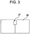
- the grooved structure 24 is formed in the magnetic sensor having the above-described structure, as shown in Fig. 3 , first, half dicing is carried out using a dicing saw that has an edge having a relatively large width to form a groove 27 in a wafer 26 having elements formed thereon. Thereafter, dicing is carried out using a dicing saw that has an edge having a relatively small width to form a chip. By carrying out such a step cutting operation, the grooved structure 24 can be provided in the magnetic sensor.
- a glass epoxy substrate having a wire that is 20 ⁇ m thick formed on one of the principal surfaces was provided.
- a magnetic sensor having electrode pads and a grooved structure such as that shown in Fig. 2 was provided.
- the pitch between the electrode pads of the magnetic sensor was 90 ⁇ m
- the size of the grooved structure was 2 ⁇ m ⁇ 30 ⁇ m.
- the distance a to an outer edge of the magnetic sensor at the grooved structure was 7 ⁇ m.
- Such a magnetic sensor was disposed so that the grooved structure faced the module substrate, and, using die-bond resin, the magnetic sensor was mounted onto the module substrate.
- the thickness b of the die-bond resin was 3 ⁇ m. That is, the thickness (20 ⁇ m) of the wire was greater than the length equal to the sum of the distance a (7 ⁇ m) from the electrode pads to an end portion of the grooved structure and the thickness b (3 ⁇ m) of the die-bond resin.
- the electrode pads and the wire of the magnetic sensor mounted in this way were subjected to corner bump bonding at an Au bump having a bump diameter of 50 ⁇ m, to produce a magnetic sensor module.
- the die-bond resin filled the grooved structure, and did not flow out to the wire.
- the pitch between the electrode pads it was possible for the pitch between the electrode pads to be 90 ⁇ m.
- the chip angle of the magnetic sensor mounted on the module substrate was a predetermined angle (that is, the sensitivity axis was oriented in a predetermined direction).
Landscapes
- Physics & Mathematics (AREA)
- Condensed Matter Physics & Semiconductors (AREA)
- General Physics & Mathematics (AREA)
- Hall/Mr Elements (AREA)
- Measuring Magnetic Variables (AREA)
Claims (3)
- Magnetsensormodul, aufweisend
ein Substrat (11);
einen Magnetsensor (13a, 13b, 13c); und
ein zweites Verbindungsmaterial (25),
wobei das Substrat (11) einen Draht (21) auf einer Hauptfläche desselben aufweist,
wobei der Magnetsensor (13a, 13b, 13c) eine auf einer Oberfläche desselben gebildete Elektrodenfläche (23) aufweist, wobei der Magnetsensor (13a, 13b, 13c) auf der Hauptfläche des Substrats (11) unter Verwendung eines ersten Verbindungsmaterials (22) derart angebracht ist, dass eine andere, zu der einen Oberfläche orthogonale Oberfläche desselben der Hauptfläche des Substrats (11) gegenüberliegt,
wobei das zweite Verbindungsmaterial (25) den Draht (21) und die Elektrodenfläche (23) elektrisch miteinander verbindet,
wobei der Magnetsensor (13a, 13b, 13c) einen Verbindungsmaterial-Aufnahmebereich aufweist, der sich zwischen der Elektrodenfläche (23) und der anderen Oberfläche befindet und der mit dem ersten Verbindungsmaterial (22) gefüllt werden kann,
wobei der Verbindungsmaterial-Aufnahmebereich derart ausgebildet ist, dass er eine Nutstruktur (24) aufweist, die an einem Endbereich in der Nähe des Drahts (21) vorgesehen ist,
dadurch gekennzeichnet,
dass ein Chipverbindungsharz als erstes Verbindungsmaterial (22) verwendet wird und das Chipverbindungsharz (22) sowohl die Nutstruktur (24) des Magnetsensors (13a, 13b, 13c) als auch eine Seite von dem Magnetsensor (13a, 13b, 13c) füllt, bei der es sich um eine dem Draht (21) gegenüberliegende Seite handelt. - Magnetsensormodul nach Anspruch 1,
wobei der Magnetsensor (13a, 13b, 13c) eine Empfindlichkeitsachse in einer zu der Hauptfläche im Wesentlichen orthogonalen Richtung aufweist. - Magnetsensormodul nach Anspruch 1,
wobei eine Dicke des Drahts (21) größer ist als eine Länge, die gleich der Summe eines Abstands von der Elektrodenfläche (23) zu dem Verbindungsmaterial-Aufnahmebereich (23) und einer Dicke des ersten Verbindungsmaterials ist.
Applications Claiming Priority (2)
| Application Number | Priority Date | Filing Date | Title |
|---|---|---|---|
| JP2007233820 | 2007-09-10 | ||
| PCT/JP2008/066292 WO2009034983A1 (ja) | 2007-09-10 | 2008-09-10 | 磁気センサモジュール |
Publications (3)
| Publication Number | Publication Date |
|---|---|
| EP2189801A1 EP2189801A1 (de) | 2010-05-26 |
| EP2189801A4 EP2189801A4 (de) | 2017-11-08 |
| EP2189801B1 true EP2189801B1 (de) | 2021-01-27 |
Family
ID=40451990
Family Applications (1)
| Application Number | Title | Priority Date | Filing Date |
|---|---|---|---|
| EP08830814.3A Active EP2189801B1 (de) | 2007-09-10 | 2008-09-10 | Magnetsensormodul |
Country Status (4)
| Country | Link |
|---|---|
| US (2) | US7868612B2 (de) |
| EP (1) | EP2189801B1 (de) |
| JP (1) | JP5150637B2 (de) |
| WO (1) | WO2009034983A1 (de) |
Families Citing this family (6)
| Publication number | Priority date | Publication date | Assignee | Title |
|---|---|---|---|---|
| EP2189801B1 (de) * | 2007-09-10 | 2021-01-27 | Alps Alpine Co., Ltd. | Magnetsensormodul |
| JP5572259B2 (ja) * | 2011-03-11 | 2014-08-13 | アルプス電気株式会社 | 物理量センサ装置とその製造方法 |
| DE102011001422A1 (de) | 2011-03-21 | 2012-09-27 | Fraunhofer-Gesellschaft zur Förderung der angewandten Forschung e.V. | Sensormodul und Verfahren zum Herstellen eines Sensormoduls |
| JP6571411B2 (ja) * | 2014-07-04 | 2019-09-04 | ローム株式会社 | 半導体装置および半導体装置の製造方法 |
| JPWO2017163815A1 (ja) * | 2016-03-22 | 2019-01-31 | パナソニックIpマネジメント株式会社 | センサ |
| DE102023212488A1 (de) * | 2023-12-11 | 2025-06-12 | Infineon Technologies Ag | Sensorvorrichtungen und zugehörige Herstellungsverfahren |
Family Cites Families (8)
| Publication number | Priority date | Publication date | Assignee | Title |
|---|---|---|---|---|
| JPH10162333A (ja) * | 1996-11-29 | 1998-06-19 | Toshiba Corp | ヘッド装置およびこれを用いた記録再生装置 |
| JP2000155922A (ja) * | 1998-11-17 | 2000-06-06 | Yamaha Corp | 磁気ヘッドのスライダ |
| JP2000215428A (ja) * | 1999-01-27 | 2000-08-04 | Tdk Corp | ヘッドスライダ支持体およびヘッド装置、ならびにそれらの製造方法 |
| JP2000298812A (ja) * | 1999-04-12 | 2000-10-24 | Hitachi Ltd | 磁気ヘッド組立体及び磁気ヘッド装置 |
| JP2002215428A (ja) | 2001-01-17 | 2002-08-02 | Nissin Electric Co Ltd | タスク監視装置、タスク監視方法及びこの方法を記録した記録媒体 |
| JP2005190534A (ja) * | 2003-12-25 | 2005-07-14 | Shinka Jitsugyo Kk | サスペンション、ヘッドジンバルアセンブリ及び該ヘッドジンバルアセンブリを備えたディスクドライブ装置 |
| JP4904052B2 (ja) * | 2005-12-27 | 2012-03-28 | アルプス電気株式会社 | 磁気方位検出装置 |
| EP2189801B1 (de) * | 2007-09-10 | 2021-01-27 | Alps Alpine Co., Ltd. | Magnetsensormodul |
-
2008
- 2008-09-10 EP EP08830814.3A patent/EP2189801B1/de active Active
- 2008-09-10 JP JP2009532192A patent/JP5150637B2/ja active Active
- 2008-09-10 WO PCT/JP2008/066292 patent/WO2009034983A1/ja not_active Ceased
-
2010
- 2010-02-17 US US12/707,263 patent/US7868612B2/en active Active
- 2010-12-06 US US12/961,235 patent/US7982460B2/en active Active
Non-Patent Citations (1)
| Title |
|---|
| None * |
Also Published As
| Publication number | Publication date |
|---|---|
| WO2009034983A1 (ja) | 2009-03-19 |
| US7868612B2 (en) | 2011-01-11 |
| JPWO2009034983A1 (ja) | 2010-12-24 |
| US20110074402A1 (en) | 2011-03-31 |
| JP5150637B2 (ja) | 2013-02-20 |
| US20100141250A1 (en) | 2010-06-10 |
| EP2189801A4 (de) | 2017-11-08 |
| US7982460B2 (en) | 2011-07-19 |
| EP2189801A1 (de) | 2010-05-26 |
Similar Documents
| Publication | Publication Date | Title |
|---|---|---|
| US6035712A (en) | Sensor device and method of producing the same using lead frame | |
| US7880290B2 (en) | Flip-chip packages allowing reduced size without electrical shorts and methods of manufacturing the same | |
| EP1401020A1 (de) | Halbleiterbauelement und herstellungsverfahren dafür | |
| KR101009121B1 (ko) | 삽입 기판에 접속하기 위한 중간 접촉자를 갖는마이크로일렉트로닉 장치, 및 중간 접촉자를 갖는마이크로일렉트로닉 장치를 패키징하는 방법 | |
| US7559148B2 (en) | Magnetic azimuth detecting device | |
| US7982460B2 (en) | Magnetic sensor module | |
| JP2004031754A (ja) | 積層マルチチップパッケージ、これを構成するチップの製造方法及びワイヤボンディング方法 | |
| KR102438605B1 (ko) | 오버 언더 센서 패키징을 위한 시스템 및 방법 | |
| JP2004032323A (ja) | 表面実装型圧電発振器及びその製造方法 | |
| EP2116858B1 (de) | Sensorchip, detektionseinrichtung und verfahren zur herstellung einer detektionseinrichtung | |
| US20130249542A1 (en) | Foldable substrate | |
| CN101958256A (zh) | 垂直传感器组装方法 | |
| US7790504B2 (en) | Integrated circuit package system | |
| US12354937B2 (en) | Semiconductor device and production method thereof | |
| US6060780A (en) | Surface mount type unit and transducer assembly using same | |
| US6531782B1 (en) | Method of placing die to minimize die-to-die routing complexity on a substrate | |
| US6111309A (en) | Semiconductor device | |
| US7553164B2 (en) | Circuit device and method of manufacturing the same | |
| JP5154275B2 (ja) | 磁気センサパッケージ | |
| US8110907B2 (en) | Semiconductor device including first substrate having plurality of wires and a plurality of first electrodes and a second substrate including a semiconductor chip being mounted thereon, and second electrodes connected with first electrodes of first substrate | |
| JP2022054045A (ja) | 慣性計測装置 | |
| KR102950559B1 (ko) | 반도체 패키지 및 그 제조 방법 | |
| JP2006275594A (ja) | 物理量センサの製造方法及びボンディング装置 | |
| US20180047629A1 (en) | Method of manufacturing semiconductor device | |
| KR20080020137A (ko) | 역피라미드 형상의 적층 반도체 패키지 |
Legal Events
| Date | Code | Title | Description |
|---|---|---|---|
| PUAI | Public reference made under article 153(3) epc to a published international application that has entered the european phase |
Free format text: ORIGINAL CODE: 0009012 |
|
| 17P | Request for examination filed |
Effective date: 20100325 |
|
| AK | Designated contracting states |
Kind code of ref document: A1 Designated state(s): AT BE BG CH CY CZ DE DK EE ES FI FR GB GR HR HU IE IS IT LI LT LU LV MC MT NL NO PL PT RO SE SI SK TR |
|
| AX | Request for extension of the european patent |
Extension state: AL BA MK RS |
|
| DAX | Request for extension of the european patent (deleted) | ||
| RA4 | Supplementary search report drawn up and despatched (corrected) |
Effective date: 20171011 |
|
| RIC1 | Information provided on ipc code assigned before grant |
Ipc: G01R 33/02 20060101AFI20171005BHEP Ipc: G01R 33/00 20060101ALI20171005BHEP |
|
| RAP1 | Party data changed (applicant data changed or rights of an application transferred) |
Owner name: ALPS ALPINE CO., LTD. |
|
| STAA | Information on the status of an ep patent application or granted ep patent |
Free format text: STATUS: EXAMINATION IS IN PROGRESS |
|
| 17Q | First examination report despatched |
Effective date: 20191126 |
|
| GRAP | Despatch of communication of intention to grant a patent |
Free format text: ORIGINAL CODE: EPIDOSNIGR1 |
|
| STAA | Information on the status of an ep patent application or granted ep patent |
Free format text: STATUS: GRANT OF PATENT IS INTENDED |
|
| INTG | Intention to grant announced |
Effective date: 20201013 |
|
| GRAS | Grant fee paid |
Free format text: ORIGINAL CODE: EPIDOSNIGR3 |
|
| GRAA | (expected) grant |
Free format text: ORIGINAL CODE: 0009210 |
|
| STAA | Information on the status of an ep patent application or granted ep patent |
Free format text: STATUS: THE PATENT HAS BEEN GRANTED |
|
| AK | Designated contracting states |
Kind code of ref document: B1 Designated state(s): AT BE BG CH CY CZ DE DK EE ES FI FR GB GR HR HU IE IS IT LI LT LU LV MC MT NL NO PL PT RO SE SI SK TR |
|
| REG | Reference to a national code |
Ref country code: GB Ref legal event code: FG4D |
|
| REG | Reference to a national code |
Ref country code: CH Ref legal event code: EP |
|
| REG | Reference to a national code |
Ref country code: AT Ref legal event code: REF Ref document number: 1360170 Country of ref document: AT Kind code of ref document: T Effective date: 20210215 |
|
| REG | Reference to a national code |
Ref country code: IE Ref legal event code: FG4D |
|
| REG | Reference to a national code |
Ref country code: DE Ref legal event code: R096 Ref document number: 602008063685 Country of ref document: DE |
|
| REG | Reference to a national code |
Ref country code: NL Ref legal event code: MP Effective date: 20210127 |
|
| REG | Reference to a national code |
Ref country code: LT Ref legal event code: MG9D |
|
| REG | Reference to a national code |
Ref country code: AT Ref legal event code: MK05 Ref document number: 1360170 Country of ref document: AT Kind code of ref document: T Effective date: 20210127 |
|
| PG25 | Lapsed in a contracting state [announced via postgrant information from national office to epo] |
Ref country code: PT Free format text: LAPSE BECAUSE OF FAILURE TO SUBMIT A TRANSLATION OF THE DESCRIPTION OR TO PAY THE FEE WITHIN THE PRESCRIBED TIME-LIMIT Effective date: 20210527 Ref country code: NO Free format text: LAPSE BECAUSE OF FAILURE TO SUBMIT A TRANSLATION OF THE DESCRIPTION OR TO PAY THE FEE WITHIN THE PRESCRIBED TIME-LIMIT Effective date: 20210427 Ref country code: NL Free format text: LAPSE BECAUSE OF FAILURE TO SUBMIT A TRANSLATION OF THE DESCRIPTION OR TO PAY THE FEE WITHIN THE PRESCRIBED TIME-LIMIT Effective date: 20210127 Ref country code: BG Free format text: LAPSE BECAUSE OF FAILURE TO SUBMIT A TRANSLATION OF THE DESCRIPTION OR TO PAY THE FEE WITHIN THE PRESCRIBED TIME-LIMIT Effective date: 20210427 Ref country code: LT Free format text: LAPSE BECAUSE OF FAILURE TO SUBMIT A TRANSLATION OF THE DESCRIPTION OR TO PAY THE FEE WITHIN THE PRESCRIBED TIME-LIMIT Effective date: 20210127 Ref country code: FI Free format text: LAPSE BECAUSE OF FAILURE TO SUBMIT A TRANSLATION OF THE DESCRIPTION OR TO PAY THE FEE WITHIN THE PRESCRIBED TIME-LIMIT Effective date: 20210127 Ref country code: GR Free format text: LAPSE BECAUSE OF FAILURE TO SUBMIT A TRANSLATION OF THE DESCRIPTION OR TO PAY THE FEE WITHIN THE PRESCRIBED TIME-LIMIT Effective date: 20210428 Ref country code: HR Free format text: LAPSE BECAUSE OF FAILURE TO SUBMIT A TRANSLATION OF THE DESCRIPTION OR TO PAY THE FEE WITHIN THE PRESCRIBED TIME-LIMIT Effective date: 20210127 |
|
| PG25 | Lapsed in a contracting state [announced via postgrant information from national office to epo] |
Ref country code: AT Free format text: LAPSE BECAUSE OF FAILURE TO SUBMIT A TRANSLATION OF THE DESCRIPTION OR TO PAY THE FEE WITHIN THE PRESCRIBED TIME-LIMIT Effective date: 20210127 Ref country code: PL Free format text: LAPSE BECAUSE OF FAILURE TO SUBMIT A TRANSLATION OF THE DESCRIPTION OR TO PAY THE FEE WITHIN THE PRESCRIBED TIME-LIMIT Effective date: 20210127 Ref country code: LV Free format text: LAPSE BECAUSE OF FAILURE TO SUBMIT A TRANSLATION OF THE DESCRIPTION OR TO PAY THE FEE WITHIN THE PRESCRIBED TIME-LIMIT Effective date: 20210127 Ref country code: SE Free format text: LAPSE BECAUSE OF FAILURE TO SUBMIT A TRANSLATION OF THE DESCRIPTION OR TO PAY THE FEE WITHIN THE PRESCRIBED TIME-LIMIT Effective date: 20210127 |
|
| PG25 | Lapsed in a contracting state [announced via postgrant information from national office to epo] |
Ref country code: IS Free format text: LAPSE BECAUSE OF FAILURE TO SUBMIT A TRANSLATION OF THE DESCRIPTION OR TO PAY THE FEE WITHIN THE PRESCRIBED TIME-LIMIT Effective date: 20210527 |
|
| REG | Reference to a national code |
Ref country code: DE Ref legal event code: R097 Ref document number: 602008063685 Country of ref document: DE |
|
| PG25 | Lapsed in a contracting state [announced via postgrant information from national office to epo] |
Ref country code: CZ Free format text: LAPSE BECAUSE OF FAILURE TO SUBMIT A TRANSLATION OF THE DESCRIPTION OR TO PAY THE FEE WITHIN THE PRESCRIBED TIME-LIMIT Effective date: 20210127 Ref country code: EE Free format text: LAPSE BECAUSE OF FAILURE TO SUBMIT A TRANSLATION OF THE DESCRIPTION OR TO PAY THE FEE WITHIN THE PRESCRIBED TIME-LIMIT Effective date: 20210127 |
|
| PG25 | Lapsed in a contracting state [announced via postgrant information from national office to epo] |
Ref country code: SK Free format text: LAPSE BECAUSE OF FAILURE TO SUBMIT A TRANSLATION OF THE DESCRIPTION OR TO PAY THE FEE WITHIN THE PRESCRIBED TIME-LIMIT Effective date: 20210127 Ref country code: ES Free format text: LAPSE BECAUSE OF FAILURE TO SUBMIT A TRANSLATION OF THE DESCRIPTION OR TO PAY THE FEE WITHIN THE PRESCRIBED TIME-LIMIT Effective date: 20210127 Ref country code: DK Free format text: LAPSE BECAUSE OF FAILURE TO SUBMIT A TRANSLATION OF THE DESCRIPTION OR TO PAY THE FEE WITHIN THE PRESCRIBED TIME-LIMIT Effective date: 20210127 Ref country code: RO Free format text: LAPSE BECAUSE OF FAILURE TO SUBMIT A TRANSLATION OF THE DESCRIPTION OR TO PAY THE FEE WITHIN THE PRESCRIBED TIME-LIMIT Effective date: 20210127 |
|
| PLBE | No opposition filed within time limit |
Free format text: ORIGINAL CODE: 0009261 |
|
| STAA | Information on the status of an ep patent application or granted ep patent |
Free format text: STATUS: NO OPPOSITION FILED WITHIN TIME LIMIT |
|
| 26N | No opposition filed |
Effective date: 20211028 |
|
| PG25 | Lapsed in a contracting state [announced via postgrant information from national office to epo] |
Ref country code: SI Free format text: LAPSE BECAUSE OF FAILURE TO SUBMIT A TRANSLATION OF THE DESCRIPTION OR TO PAY THE FEE WITHIN THE PRESCRIBED TIME-LIMIT Effective date: 20210127 |
|
| PG25 | Lapsed in a contracting state [announced via postgrant information from national office to epo] |
Ref country code: IT Free format text: LAPSE BECAUSE OF FAILURE TO SUBMIT A TRANSLATION OF THE DESCRIPTION OR TO PAY THE FEE WITHIN THE PRESCRIBED TIME-LIMIT Effective date: 20210127 |
|
| REG | Reference to a national code |
Ref country code: CH Ref legal event code: PL |
|
| REG | Reference to a national code |
Ref country code: BE Ref legal event code: MM Effective date: 20210930 |
|
| GBPC | Gb: european patent ceased through non-payment of renewal fee |
Effective date: 20210910 |
|
| PG25 | Lapsed in a contracting state [announced via postgrant information from national office to epo] |
Ref country code: IS Free format text: LAPSE BECAUSE OF FAILURE TO SUBMIT A TRANSLATION OF THE DESCRIPTION OR TO PAY THE FEE WITHIN THE PRESCRIBED TIME-LIMIT Effective date: 20210527 Ref country code: MC Free format text: LAPSE BECAUSE OF FAILURE TO SUBMIT A TRANSLATION OF THE DESCRIPTION OR TO PAY THE FEE WITHIN THE PRESCRIBED TIME-LIMIT Effective date: 20210127 |
|
| PG25 | Lapsed in a contracting state [announced via postgrant information from national office to epo] |
Ref country code: LU Free format text: LAPSE BECAUSE OF NON-PAYMENT OF DUE FEES Effective date: 20210910 Ref country code: IE Free format text: LAPSE BECAUSE OF NON-PAYMENT OF DUE FEES Effective date: 20210910 Ref country code: GB Free format text: LAPSE BECAUSE OF NON-PAYMENT OF DUE FEES Effective date: 20210910 Ref country code: FR Free format text: LAPSE BECAUSE OF NON-PAYMENT OF DUE FEES Effective date: 20210930 Ref country code: BE Free format text: LAPSE BECAUSE OF NON-PAYMENT OF DUE FEES Effective date: 20210930 |
|
| PG25 | Lapsed in a contracting state [announced via postgrant information from national office to epo] |
Ref country code: LI Free format text: LAPSE BECAUSE OF NON-PAYMENT OF DUE FEES Effective date: 20210930 Ref country code: CH Free format text: LAPSE BECAUSE OF NON-PAYMENT OF DUE FEES Effective date: 20210930 |
|
| PG25 | Lapsed in a contracting state [announced via postgrant information from national office to epo] |
Ref country code: HU Free format text: LAPSE BECAUSE OF FAILURE TO SUBMIT A TRANSLATION OF THE DESCRIPTION OR TO PAY THE FEE WITHIN THE PRESCRIBED TIME-LIMIT; INVALID AB INITIO Effective date: 20080910 Ref country code: CY Free format text: LAPSE BECAUSE OF FAILURE TO SUBMIT A TRANSLATION OF THE DESCRIPTION OR TO PAY THE FEE WITHIN THE PRESCRIBED TIME-LIMIT Effective date: 20210127 |
|
| PG25 | Lapsed in a contracting state [announced via postgrant information from national office to epo] |
Ref country code: MT Free format text: LAPSE BECAUSE OF FAILURE TO SUBMIT A TRANSLATION OF THE DESCRIPTION OR TO PAY THE FEE WITHIN THE PRESCRIBED TIME-LIMIT Effective date: 20210127 |
|
| PGFP | Annual fee paid to national office [announced via postgrant information from national office to epo] |
Ref country code: DE Payment date: 20250919 Year of fee payment: 18 |
|
| PG25 | Lapsed in a contracting state [announced via postgrant information from national office to epo] |
Ref country code: TR Free format text: LAPSE BECAUSE OF FAILURE TO SUBMIT A TRANSLATION OF THE DESCRIPTION OR TO PAY THE FEE WITHIN THE PRESCRIBED TIME-LIMIT Effective date: 20210127 |