EP2182632B1 - Broadband microwave amplifier - Google Patents
Broadband microwave amplifier Download PDFInfo
- Publication number
- EP2182632B1 EP2182632B1 EP10152522A EP10152522A EP2182632B1 EP 2182632 B1 EP2182632 B1 EP 2182632B1 EP 10152522 A EP10152522 A EP 10152522A EP 10152522 A EP10152522 A EP 10152522A EP 2182632 B1 EP2182632 B1 EP 2182632B1
- Authority
- EP
- European Patent Office
- Prior art keywords
- load
- class
- drain
- amplifier
- circuit representation
- Prior art date
- Legal status (The legal status is an assumption and is not a legal conclusion. Google has not performed a legal analysis and makes no representation as to the accuracy of the status listed.)
- Expired - Lifetime
Links
Images


Classifications
-
- H—ELECTRICITY
- H03—ELECTRONIC CIRCUITRY
- H03F—AMPLIFIERS
- H03F3/00—Amplifiers with only discharge tubes or only semiconductor devices as amplifying elements
- H03F3/20—Power amplifiers, e.g. Class B amplifiers, Class C amplifiers
- H03F3/21—Power amplifiers, e.g. Class B amplifiers, Class C amplifiers with semiconductor devices only
- H03F3/217—Class D power amplifiers; Switching amplifiers
- H03F3/2176—Class E amplifiers
-
- H—ELECTRICITY
- H03—ELECTRONIC CIRCUITRY
- H03H—IMPEDANCE NETWORKS, e.g. RESONANT CIRCUITS; RESONATORS
- H03H7/00—Multiple-port networks comprising only passive electrical elements as network components
- H03H7/38—Impedance-matching networks
-
- H—ELECTRICITY
- H03—ELECTRONIC CIRCUITRY
- H03F—AMPLIFIERS
- H03F2200/00—Indexing scheme relating to amplifiers
- H03F2200/03—Indexing scheme relating to amplifiers the amplifier being designed for audio applications
Definitions
- the present invention relates to electrical and electronic circuits and systems. More specifically, the present invention relates to microwave Class E power amplifiers.
- RF radio frequency
- Typical applications include wireless local area networks, cell phones and telecommunication systems as well as advanced airborne active phased array radar systems.
- the choice of technology, design methodology and manufacturing cycle time are major cost contributors in these systems.
- Switching mode, Class-E, high-efficiency power amplifiers are useful for these and other applications inasmuch as these amplifiers limit the power and associated cooling costs thereof.
- a Class-E amplifier is part of the "switching mode amplifiers" such as class D, E, F, etc. In these types of amplifiers, the transistor operates as a perfect switch with no overlapping voltage & current waveforms at its output terminal, thereby ideally dissipating zero DC power.
- Class-E amplifiers as described in US 2004/0113689 A1 , use a series or parallel resonant load network.
- the function of the load network in the class-E amplifier is to shape the voltage and current waveforms.
- the current and voltage time-waveforms at the active device output terminal are optimized in such a way as to minimize the DC power dissipation within.
- the active device a pHEMT in this case, acts as a switch, driven by the RF input signal to "ON" and "OFF" conditions.
- the operating point of the device is such that the device is either OFF (in the pinched-off region) or ON (in the linear region). Under an ideal switching operation condition, output voltage and current waveforms at the device output terminal do not exist simultaneously and, therefore, the energy dissipated within the device is zero, yielding a 100 percent theoretical power conversion efficiency.
- document US 3 919 656 A shows another high-efficiency tuned switching power amplifier.
- the maximum efficiency of Class-E amplifiers i.e. the ratio of the RF output power to the DC input power
- its bandwidth of operation are limited by the tuned loads thereof.
- the limitation is due to the fact that presence of the tuned load results in a very narrow operational bandwidth for the amplifier.
- a method for designing a load for use with a class-E amplifier having a transistor switch including the steps of: providing a lumped equivalent circuit representation of the load, including a shunt capacitor (15) which is the drain to source capacitance (C ds ) of the transistor switch (12), and including a drain bias inductor as a part of the Class-E load topology; optimizing the lumped equivalent circuit representation of the load to achieve near ideal current and voltage operational characteristics over a predetermined frequency range using a time domain simulation; transforming the optimized lumped equivalent circuit representation of the load to a distributed circuit representation wherein the drain bias inductor is replaced with a shunt shorted stub to provide a parallel resonance with the drain to source capacitance as well as to provide a bias to the drain of the transistor switch; and optimizing the distributed circuit representation of the load to achieve near ideal current and voltage operational characteristics over a predetermined frequency range using a time domain simulation.
- Load circuit topologies designed according to the present invention are suitable for switching mode Power Amplifiers (PAs).
- the designed load includes a shunt inductive element coupled to an output of said amplifier; a series inductive element coupled to said output of said amplifier; and a series capacitive element coupled to said series inductive element.
- the designed load is operable at frequencies in the range of 8 - 10 GHz and beyond.
- the shunt inductive element, part of the said load is suitably chosen to provide two important functions. First, to provide an inductive bias line for said amplifier and second, to provide a parallel resonance with the pHEMT's output drain-source capacitance (Cds).
- the invention enables an advantageous class-E amplifier design comprising an input matching network; an active device coupled to the input matching network and a load coupled to the active device and implemented in accordance with the present teachings.
- the unique properties of the inventive load circuits enable Class-E HPAs to maintain a simultaneous high PAE and Power over a broad bandwidth.
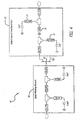
- Fig. 1a is a simplified schematic diagram of an ideal discrete component implementation of a typical Class-E load in accordance with conventional teachings.
- a typical Class-E amplifier represented by a switch 12' is coupled to a source V ds via an inductive bias line 14'.
- the switch 12' is coupled to a resistive load 24' via a capacitor 22' and an inverted L type (series L, shunt C) wave shaping load network 20'.
- the drain bias line 14' is treated independent of the load circuit 20', merely acting as a choke realized by a quarter wavelength length of transmission line.
- the load 20' includes a first shunt capacitor 15' which is the drain to source capacitance (C ds ) of the transistor switch 12'.
- the load 20' includes a series inductor 16' (L) and a shunt capacitor 18' (C).
- Fig. 1b is a distributed component implementation of the load depicted in Fig. 1a .
- the function of the load network in the class E amplifier is to shape the voltage and current waveforms. Therefore, for the design of a broadband Class-E amplifier, care should be taken to ensure Class-E waveforms exist over the entire frequency band.
- Choices of a suitable device non-linear modeling tool as well as a design environment tool capable of time domain, robust harmonic balance and envelope simulation are critical for the successful design of highly non-linear circuits such as the switching mode amplifiers.
- Fig. 2a is a simplified schematic diagram of an ideal discrete component implementation of a typical Class-E load in accordance with the teachings of the present invention.
- Fig. 2b is a distributed component implementation of the load depicted in Fig. 2a .
- a novel broadband Class-E load topology is presented based on the series (L-C) network shown in Fig. 2a .
- the load is modified to offer a superior broadband performance when compared with the (series L, shunt C) load network of Figs. 1a and 1b .
- the first step in the novel design process is to include the drain bias inductor 14 as part of the Class-E load topology followed by the transformation of the lumped network representation to its equivalent distributed network form.
- the series inductor 16 and series capacitor 18 of Fig. 2a are replaced by a combination of a series transmission line and a shunt shorted stub as shown in Fig 2b .
- the shunt inductor 14 of Fig. 2a is replaced with a shunt shorted stub to provide a parallel resonance with the pHEMT's output drain-source capacitance (Cds) as well as to provide a bias to the drain of the pHEMT transistor.
- a time domain simulation is performed to optimize the load with the objective of obtaining near ideal current and voltage waveforms over a desired operating range (e.g. 8 - 10 GHz).
- Fig. 2c shows these simulated waveforms illustrating near ideal performance over 2.0 GHz of bandwidth.
- the frequency dependency of the broadband lumped equivalent circuit representation of the load is shown in Fig. 3 (a) , depicting an excellent frequency independent response over 8.0-10.0 GHz compared to the narrowband Class-E load (series L, shunt C). See " A Monolithic X-band Class-E Power Amplifier", by R. Tayrani, IEEE GaAs IC Symposium, PP 205-208, Oct. 2001 .
- Figure 3b is a diagram which illustrates the time domain simulation of the distributed load network illustrating near ideal performance at 8 GHz. As shown in Figure 3b , the voltage waveform across the switch rises slowly at switch-off and falls to zero at the end of the half-cycle. It also has a zero rate of change at the end of half-cycle, thereby ensuring a "soft" turn-on condition.
- the load circuit is synthesized for medium power PAs ( ⁇ 30 dBm, 1.0 W max).
- a single 0.25 um x 720 um pHEMT device is used in this circuit.
- Such PAs are suitable as a single stage PA and/or as the first stage of a two stage Class-E High Power Amplifiers (HPAs).
- Figure 4 shows a schematic circuit of a distributed representation of a monolithic Class-E amplifier with the broadband Class-E load in accordance with the present teachings.
- the amplifier 30 of Fig. 4 includes an active device 12 with the inventive load 20.
- the active device 12 is a Gallium-Arsenide pseudo-morphic, high-electron mobility transistor (GaAs pHEMT).
- An input matching network 40 is provided at the input to the active device 12.
- the load 20 and input matching network 40 are designed with the width and length dimensions shown in microns for operation at 8 - 10 Ghz. Those of ordinary skill in the art may extend the present teachings to other frequencies without departing from the scope thereof.
- the device non-linear model should have the following properties:
- the device model should be able to accurately model the dispersion associated with the drain current, gm, and R ds . If the pulsed DC IV technique is used for the model development, this requirement may be unnecessary.
- the EEHEMT model available in ICCAP (Agilent ICCAP, V.5.1) and ADS (Agilent Advanced Design Systems (ADS), V. 2003C).
- a 0.3 ⁇ m x 6 x 120 ⁇ m pHEMT device having a gate-drain breakdown voltage of greater than 18 V may be designed using currently available technology in accordance with the present teachings to meet performance goals for very large (>100,000 T/R elements) space based phased array radar requiring simultaneous broadband power (min. 200.0 mW) and PAE (min. 60%) over 8.0 - 10.0 GHz.
- Figure 5 depicts simulated voltage and current waveforms at the pHEMT output terminals of the amplifier of Fig 4 .
- the waveforms show a switching mode behavior of the pHEMT device at 8.5 GHz. Similar waveforms may be provided over 8 - 10 GHz to confirm broadband operation.
- the present invention has been described herein with reference to a particular embodiment for a particular application. Those having ordinary skill in the art and access to the present teachings will recognize additional modifications applications and embodiments within the scope thereof.
- the present teachings are not limited to Class-E amplifiers. That is, the present teachings may be used in connection with any switching amplifier or circuit design.
Landscapes
- Engineering & Computer Science (AREA)
- Power Engineering (AREA)
- Amplifiers (AREA)
- Microwave Amplifiers (AREA)
- Stabilization Of Oscillater, Synchronisation, Frequency Synthesizers (AREA)
- Control Of Motors That Do Not Use Commutators (AREA)
Applications Claiming Priority (2)
| Application Number | Priority Date | Filing Date | Title |
|---|---|---|---|
| US11/054,968 US7345539B2 (en) | 2005-02-10 | 2005-02-10 | Broadband microwave amplifier |
| EP06720546A EP1849232A1 (en) | 2005-02-10 | 2006-02-09 | Broadband microwave amplifier |
Related Parent Applications (1)
| Application Number | Title | Priority Date | Filing Date |
|---|---|---|---|
| EP06720546.8 Division | 2006-02-09 |
Publications (2)
| Publication Number | Publication Date |
|---|---|
| EP2182632A1 EP2182632A1 (en) | 2010-05-05 |
| EP2182632B1 true EP2182632B1 (en) | 2013-01-02 |
Family
ID=36499224
Family Applications (2)
| Application Number | Title | Priority Date | Filing Date |
|---|---|---|---|
| EP10152522A Expired - Lifetime EP2182632B1 (en) | 2005-02-10 | 2006-02-09 | Broadband microwave amplifier |
| EP06720546A Withdrawn EP1849232A1 (en) | 2005-02-10 | 2006-02-09 | Broadband microwave amplifier |
Family Applications After (1)
| Application Number | Title | Priority Date | Filing Date |
|---|---|---|---|
| EP06720546A Withdrawn EP1849232A1 (en) | 2005-02-10 | 2006-02-09 | Broadband microwave amplifier |
Country Status (8)
| Country | Link |
|---|---|
| US (1) | US7345539B2 (https=) |
| EP (2) | EP2182632B1 (https=) |
| JP (2) | JP2008530910A (https=) |
| KR (1) | KR20070096015A (https=) |
| CA (1) | CA2577791C (https=) |
| DK (1) | DK2182632T3 (https=) |
| NO (2) | NO20074547L (https=) |
| WO (1) | WO2006086542A1 (https=) |
Cited By (1)
| Publication number | Priority date | Publication date | Assignee | Title |
|---|---|---|---|---|
| CN107547050A (zh) * | 2017-08-21 | 2018-01-05 | 天津大学 | 一种双级双频带高效功率放大器 |
Families Citing this family (8)
| Publication number | Priority date | Publication date | Assignee | Title |
|---|---|---|---|---|
| JP5419812B2 (ja) * | 2010-06-30 | 2014-02-19 | 三菱電機株式会社 | 高周波多段能動回路 |
| FR2965082B1 (fr) | 2010-09-21 | 2012-09-28 | Inside Contactless | Procede et dispositif de modulation de charge active par couplage inductif |
| JP5759286B2 (ja) * | 2011-06-27 | 2015-08-05 | 住友電気工業株式会社 | スイッチング回路 |
| WO2013066466A2 (en) * | 2011-08-12 | 2013-05-10 | Bae Systems Integration And Electronic Systems Integration Inc. | Low voltage high efficiency gallium arsenide power amplifier |
| US8456238B1 (en) | 2012-03-30 | 2013-06-04 | Centellax, Inc. | Tapered attenuator network for mitigating effects of direct current (DC) bias inductor self-resonance in traveling wave amplifiers |
| JP6049673B2 (ja) * | 2014-10-31 | 2016-12-21 | 株式会社東芝 | 半導体増幅装置 |
| CN105550790B (zh) * | 2016-03-08 | 2019-08-06 | 重庆大学 | 基于非拓扑法等值的互联电网无功优化计算方法 |
| CN111985177B (zh) * | 2020-06-30 | 2023-05-02 | 宁波大学 | 一种射频功率放大器的设计方法 |
Family Cites Families (22)
| Publication number | Priority date | Publication date | Assignee | Title |
|---|---|---|---|---|
| US3919656A (en) | 1973-04-23 | 1975-11-11 | Nathan O Sokal | High-efficiency tuned switching power amplifier |
| JPS59814Y2 (ja) * | 1977-04-22 | 1984-01-11 | ブライアン・ア−ネスト・アトウツド | D級増幅器 |
| US4717884A (en) * | 1986-04-14 | 1988-01-05 | Motorola, Inc. | High efficiency RF power amplifier |
| US4763087A (en) | 1986-05-27 | 1988-08-09 | Schrader Paul D | Impedance matching network |
| JPS63279608A (ja) * | 1987-05-11 | 1988-11-16 | Nippon Telegr & Teleph Corp <Ntt> | 増幅器集積回路 |
| JPH0732335B2 (ja) | 1990-11-16 | 1995-04-10 | 日本電信電話株式会社 | 高周波増幅器 |
| DE69221716T2 (de) * | 1991-02-04 | 1997-12-18 | Advanced Energy Ind Inc | Verfahren und Vorrichtung zur Hochleistungsrundfunkfrequenzverstärkungim Schaltbetrieb |
| JPH0554094A (ja) * | 1991-08-23 | 1993-03-05 | Mitsubishi Electric Corp | 回路シミユレーシヨン装置 |
| JP2627113B2 (ja) * | 1992-01-16 | 1997-07-02 | 岩崎通信機株式会社 | 高周波電力増幅器 |
| JPH06196902A (ja) * | 1992-12-25 | 1994-07-15 | Akira Ogawa | バンドパスフィルタ |
| US6121840A (en) * | 1996-12-24 | 2000-09-19 | Murata Manufacturing Co., Ltd. | High-frequency amplifier |
| JP4157619B2 (ja) * | 1997-09-24 | 2008-10-01 | 東芝キヤリア株式会社 | 空気調和機 |
| JP2000165175A (ja) | 1998-11-27 | 2000-06-16 | Kyosan Electric Mfg Co Ltd | インピーダンス整合装置 |
| JP2000341162A (ja) * | 1999-05-31 | 2000-12-08 | Debon Multimedia Kk | 周波数が異なる2つの搬送波を分波及び合成する共用装置、及び、該共用装置を利用した周波数が異なる2つの搬送波の伝播方法 |
| US6232841B1 (en) | 1999-07-01 | 2001-05-15 | Rockwell Science Center, Llc | Integrated tunable high efficiency power amplifier |
| US6469919B1 (en) * | 1999-07-22 | 2002-10-22 | Eni Technology, Inc. | Power supplies having protection circuits |
| CN1295865C (zh) | 2000-10-10 | 2007-01-17 | 加利福尼亚技术协会 | E/f类开关功率放大器 |
| US6603352B2 (en) * | 2001-12-03 | 2003-08-05 | Icefyre Semiconductor Corporation | Switched-mode power amplifier integrally performing power combining |
| US6552610B1 (en) * | 2002-01-15 | 2003-04-22 | Mva.Com Eurotec, B.V. | Transmission-line tuned switching power amplifier |
| US6806767B2 (en) * | 2002-07-09 | 2004-10-19 | Anadigics, Inc. | Power amplifier with load switching circuit |
| US20040027209A1 (en) | 2002-08-09 | 2004-02-12 | Applied Materials, Inc. | Fixed matching network with increased match range capabilities |
| US6949978B2 (en) * | 2003-10-17 | 2005-09-27 | Raytheon Company | Efficient broadband switching-mode amplifier |
-
2005
- 2005-02-10 US US11/054,968 patent/US7345539B2/en not_active Expired - Lifetime
-
2006
- 2006-02-09 KR KR1020077018416A patent/KR20070096015A/ko not_active Ceased
- 2006-02-09 DK DK10152522.8T patent/DK2182632T3/da active
- 2006-02-09 CA CA2577791A patent/CA2577791C/en not_active Expired - Lifetime
- 2006-02-09 WO PCT/US2006/004554 patent/WO2006086542A1/en not_active Ceased
- 2006-02-09 EP EP10152522A patent/EP2182632B1/en not_active Expired - Lifetime
- 2006-02-09 JP JP2007555213A patent/JP2008530910A/ja not_active Withdrawn
- 2006-02-09 EP EP06720546A patent/EP1849232A1/en not_active Withdrawn
-
2007
- 2007-09-07 NO NO20074547A patent/NO20074547L/no not_active Application Discontinuation
-
2012
- 2012-06-21 JP JP2012139986A patent/JP5362884B2/ja not_active Expired - Fee Related
-
2017
- 2017-01-16 NO NO20170060A patent/NO340987B1/no unknown
Cited By (2)
| Publication number | Priority date | Publication date | Assignee | Title |
|---|---|---|---|---|
| CN107547050A (zh) * | 2017-08-21 | 2018-01-05 | 天津大学 | 一种双级双频带高效功率放大器 |
| CN107547050B (zh) * | 2017-08-21 | 2020-12-15 | 天津大学 | 一种双级双频带高效功率放大器 |
Also Published As
| Publication number | Publication date |
|---|---|
| KR20070096015A (ko) | 2007-10-01 |
| US7345539B2 (en) | 2008-03-18 |
| DK2182632T3 (da) | 2013-03-25 |
| JP5362884B2 (ja) | 2013-12-11 |
| JP2012231506A (ja) | 2012-11-22 |
| CA2577791A1 (en) | 2006-08-17 |
| EP1849232A1 (en) | 2007-10-31 |
| JP2008530910A (ja) | 2008-08-07 |
| NO20074547L (no) | 2007-10-29 |
| US20060176114A1 (en) | 2006-08-10 |
| CA2577791C (en) | 2010-11-23 |
| WO2006086542A1 (en) | 2006-08-17 |
| NO340987B1 (no) | 2017-07-31 |
| NO20170060A1 (no) | 2017-01-16 |
| EP2182632A1 (en) | 2010-05-05 |
Similar Documents
| Publication | Publication Date | Title |
|---|---|---|
| JP5362884B2 (ja) | 広帯域マイクロ波増幅器 | |
| JP5512731B2 (ja) | 2段のマイクロ波のe級電力増幅器 | |
| Song et al. | A CMOS class-E power amplifier with voltage stress relief and enhanced efficiency | |
| Lee et al. | A CMOS outphasing power amplifier with integrated single-ended Chireix combiner | |
| Mansour et al. | A reconfigurable class-AB/F power amplifier for 0.1–4.2 GHz multistandard applications | |
| Meshkin et al. | A novel 2.4 GHz CMOS class-E power amplifier with efficient power control for wireless communications | |
| Zarghami et al. | A novel design methodology for extended continuous class-F power amplifiers in wireless applications | |
| Tayrani | A broadband monolithic S-band class-E power amplifier | |
| Lin et al. | A 20 w gan hemt vhf/uhf class-d power amplifier | |
| CN115514325A (zh) | 一种l波段单片集成功率放大器 | |
| Liu et al. | A class-E RF power amplifier with a novel matching network for high-efficiency dynamic load modulation | |
| Khan et al. | Design of a broadband current mode class-D power amplifier with harmonic suppression | |
| Tayrani | A highly efficient broadband (7-14 GHz) monolithic class e power amplifier for space based radar | |
| Lin et al. | Development of a wideband highly efficient GaN VMCD VHF/UHF power amplifier | |
| Moon et al. | A multimode/multiband envelope tracking transmitter with broadband saturated power amplifier | |
| Dehqan et al. | Resonance gate bias cascode class-E power amplifier in GaAs pHEMT technology | |
| Medina Gómez et al. | Load-independent class-E/F2 topologies for low-loss UHF power inverters | |
| Zhang et al. | Design of Reconfigurable Broadband Power Amplifier | |
| Medina et al. | Load-Independent Class-E/F2 Topologies for Low-Loss UHF Power Inverters | |
| Aruna et al. | Efficiency enchancement of Class-E power amplifier in VHF radio frequency spectrum for land mobile radio system | |
| KIRISH | DESIGN OF DUAL-BAND MATCHING NETWORK FOR HIGHLY EFFICIENT POWER AMPLIFIER. | |
| CN112653405A (zh) | 宽带功率放大器及其构造方法 | |
| Panda et al. | An Efficient And Power Optimized Cascode Stage RF Tuned Class-E Power Amplifier | |
| Shukla et al. | A Comparative Analysis between GaN-Based Current and Voltage Mode Class-D and E PAs for Communications | |
| Aflaki et al. | 1 GHz Current Mode Class-D Power Amplifier in Hybrid Technology Using GaN HEMTs |
Legal Events
| Date | Code | Title | Description |
|---|---|---|---|
| PUAI | Public reference made under article 153(3) epc to a published international application that has entered the european phase |
Free format text: ORIGINAL CODE: 0009012 |
|
| 17P | Request for examination filed |
Effective date: 20100203 |
|
| AC | Divisional application: reference to earlier application |
Ref document number: 1849232 Country of ref document: EP Kind code of ref document: P |
|
| AK | Designated contracting states |
Kind code of ref document: A1 Designated state(s): DE DK FR IT NL SE |
|
| RBV | Designated contracting states (corrected) |
Designated state(s): AT BE BG CH CY CZ DE DK EE ES FI FR GB GR HU IE IS IT LI LT LU LV MC NL PL PT RO SE SI SK TR |
|
| 17Q | First examination report despatched |
Effective date: 20100723 |
|
| REG | Reference to a national code |
Ref country code: DE Ref legal event code: R079 Ref document number: 602006034051 Country of ref document: DE Free format text: PREVIOUS MAIN CLASS: H03F0003217000 Ipc: H03H0007380000 |
|
| GRAP | Despatch of communication of intention to grant a patent |
Free format text: ORIGINAL CODE: EPIDOSNIGR1 |
|
| RIC1 | Information provided on ipc code assigned before grant |
Ipc: H03H 7/38 20060101AFI20120627BHEP Ipc: H03F 3/217 20060101ALI20120627BHEP |
|
| RBV | Designated contracting states (corrected) |
Designated state(s): DE DK FR IT NL SE |
|
| GRAS | Grant fee paid |
Free format text: ORIGINAL CODE: EPIDOSNIGR3 |
|
| GRAA | (expected) grant |
Free format text: ORIGINAL CODE: 0009210 |
|
| AC | Divisional application: reference to earlier application |
Ref document number: 1849232 Country of ref document: EP Kind code of ref document: P |
|
| AK | Designated contracting states |
Kind code of ref document: B1 Designated state(s): DE DK FR IT NL SE |
|
| REG | Reference to a national code |
Ref country code: SE Ref legal event code: TRGR |
|
| REG | Reference to a national code |
Ref country code: DE Ref legal event code: R096 Ref document number: 602006034051 Country of ref document: DE Effective date: 20130228 |
|
| REG | Reference to a national code |
Ref country code: DK Ref legal event code: T3 |
|
| REG | Reference to a national code |
Ref country code: NL Ref legal event code: T3 |
|
| PLBE | No opposition filed within time limit |
Free format text: ORIGINAL CODE: 0009261 |
|
| STAA | Information on the status of an ep patent application or granted ep patent |
Free format text: STATUS: NO OPPOSITION FILED WITHIN TIME LIMIT |
|
| 26N | No opposition filed |
Effective date: 20131003 |
|
| REG | Reference to a national code |
Ref country code: DE Ref legal event code: R097 Ref document number: 602006034051 Country of ref document: DE Effective date: 20131003 |
|
| REG | Reference to a national code |
Ref country code: FR Ref legal event code: PLFP Year of fee payment: 11 |
|
| REG | Reference to a national code |
Ref country code: FR Ref legal event code: PLFP Year of fee payment: 12 |
|
| REG | Reference to a national code |
Ref country code: FR Ref legal event code: PLFP Year of fee payment: 13 |
|
| PGFP | Annual fee paid to national office [announced via postgrant information from national office to epo] |
Ref country code: SE Payment date: 20220120 Year of fee payment: 17 |
|
| PGFP | Annual fee paid to national office [announced via postgrant information from national office to epo] |
Ref country code: FR Payment date: 20230119 Year of fee payment: 18 Ref country code: DK Payment date: 20230119 Year of fee payment: 18 |
|
| PGFP | Annual fee paid to national office [announced via postgrant information from national office to epo] |
Ref country code: IT Payment date: 20230120 Year of fee payment: 18 Ref country code: DE Payment date: 20230119 Year of fee payment: 18 |
|
| PGFP | Annual fee paid to national office [announced via postgrant information from national office to epo] |
Ref country code: NL Payment date: 20230119 Year of fee payment: 18 |
|
| REG | Reference to a national code |
Ref country code: SE Ref legal event code: EUG |
|
| PG25 | Lapsed in a contracting state [announced via postgrant information from national office to epo] |
Ref country code: SE Free format text: LAPSE BECAUSE OF NON-PAYMENT OF DUE FEES Effective date: 20230210 |
|
| REG | Reference to a national code |
Ref country code: DE Ref legal event code: R119 Ref document number: 602006034051 Country of ref document: DE |
|
| REG | Reference to a national code |
Ref country code: DK Ref legal event code: EBP Effective date: 20240229 |
|
| REG | Reference to a national code |
Ref country code: NL Ref legal event code: MM Effective date: 20240301 |
|
| PG25 | Lapsed in a contracting state [announced via postgrant information from national office to epo] |
Ref country code: NL Free format text: LAPSE BECAUSE OF NON-PAYMENT OF DUE FEES Effective date: 20240301 |
|
| PG25 | Lapsed in a contracting state [announced via postgrant information from national office to epo] |
Ref country code: NL Free format text: LAPSE BECAUSE OF NON-PAYMENT OF DUE FEES Effective date: 20240301 |
|
| PG25 | Lapsed in a contracting state [announced via postgrant information from national office to epo] |
Ref country code: DE Free format text: LAPSE BECAUSE OF NON-PAYMENT OF DUE FEES Effective date: 20240903 |
|
| PG25 | Lapsed in a contracting state [announced via postgrant information from national office to epo] |
Ref country code: DK Free format text: LAPSE BECAUSE OF NON-PAYMENT OF DUE FEES Effective date: 20240229 |
|
| PG25 | Lapsed in a contracting state [announced via postgrant information from national office to epo] |
Ref country code: FR Free format text: LAPSE BECAUSE OF NON-PAYMENT OF DUE FEES Effective date: 20240229 |
|
| PG25 | Lapsed in a contracting state [announced via postgrant information from national office to epo] |
Ref country code: FR Free format text: LAPSE BECAUSE OF NON-PAYMENT OF DUE FEES Effective date: 20240229 Ref country code: DK Free format text: LAPSE BECAUSE OF NON-PAYMENT OF DUE FEES Effective date: 20240229 Ref country code: DE Free format text: LAPSE BECAUSE OF NON-PAYMENT OF DUE FEES Effective date: 20240903 |
|
| PG25 | Lapsed in a contracting state [announced via postgrant information from national office to epo] |
Ref country code: IT Free format text: LAPSE BECAUSE OF NON-PAYMENT OF DUE FEES Effective date: 20240209 |