EP2182632B1 - Broadband microwave amplifier - Google Patents
Broadband microwave amplifier Download PDFInfo
- Publication number
- EP2182632B1 EP2182632B1 EP10152522A EP10152522A EP2182632B1 EP 2182632 B1 EP2182632 B1 EP 2182632B1 EP 10152522 A EP10152522 A EP 10152522A EP 10152522 A EP10152522 A EP 10152522A EP 2182632 B1 EP2182632 B1 EP 2182632B1
- Authority
- EP
- European Patent Office
- Prior art keywords
- load
- class
- drain
- amplifier
- circuit representation
- Prior art date
- Legal status (The legal status is an assumption and is not a legal conclusion. Google has not performed a legal analysis and makes no representation as to the accuracy of the status listed.)
- Active
Links
Images


Classifications
-
- H—ELECTRICITY
- H03—ELECTRONIC CIRCUITRY
- H03F—AMPLIFIERS
- H03F3/00—Amplifiers with only discharge tubes or only semiconductor devices as amplifying elements
- H03F3/20—Power amplifiers, e.g. Class B amplifiers, Class C amplifiers
- H03F3/21—Power amplifiers, e.g. Class B amplifiers, Class C amplifiers with semiconductor devices only
- H03F3/217—Class D power amplifiers; Switching amplifiers
- H03F3/2176—Class E amplifiers
-
- H—ELECTRICITY
- H03—ELECTRONIC CIRCUITRY
- H03H—IMPEDANCE NETWORKS, e.g. RESONANT CIRCUITS; RESONATORS
- H03H7/00—Multiple-port networks comprising only passive electrical elements as network components
- H03H7/38—Impedance-matching networks
-
- H—ELECTRICITY
- H03—ELECTRONIC CIRCUITRY
- H03F—AMPLIFIERS
- H03F2200/00—Indexing scheme relating to amplifiers
- H03F2200/03—Indexing scheme relating to amplifiers the amplifier being designed for audio applications
Definitions
- the present invention relates to electrical and electronic circuits and systems. More specifically, the present invention relates to microwave Class E power amplifiers.
- RF radio frequency
- Typical applications include wireless local area networks, cell phones and telecommunication systems as well as advanced airborne active phased array radar systems.
- the choice of technology, design methodology and manufacturing cycle time are major cost contributors in these systems.
- Switching mode, Class-E, high-efficiency power amplifiers are useful for these and other applications inasmuch as these amplifiers limit the power and associated cooling costs thereof.
- a Class-E amplifier is part of the "switching mode amplifiers" such as class D, E, F, etc. In these types of amplifiers, the transistor operates as a perfect switch with no overlapping voltage & current waveforms at its output terminal, thereby ideally dissipating zero DC power.
- Class-E amplifiers as described in US 2004/0113689 A1 , use a series or parallel resonant load network.
- the function of the load network in the class-E amplifier is to shape the voltage and current waveforms.
- the current and voltage time-waveforms at the active device output terminal are optimized in such a way as to minimize the DC power dissipation within.
- the active device a pHEMT in this case, acts as a switch, driven by the RF input signal to "ON" and "OFF" conditions.
- the operating point of the device is such that the device is either OFF (in the pinched-off region) or ON (in the linear region). Under an ideal switching operation condition, output voltage and current waveforms at the device output terminal do not exist simultaneously and, therefore, the energy dissipated within the device is zero, yielding a 100 percent theoretical power conversion efficiency.
- document US 3 919 656 A shows another high-efficiency tuned switching power amplifier.
- the maximum efficiency of Class-E amplifiers i.e. the ratio of the RF output power to the DC input power
- its bandwidth of operation are limited by the tuned loads thereof.
- the limitation is due to the fact that presence of the tuned load results in a very narrow operational bandwidth for the amplifier.
- a method for designing a load for use with a class-E amplifier having a transistor switch including the steps of: providing a lumped equivalent circuit representation of the load, including a shunt capacitor (15) which is the drain to source capacitance (C ds ) of the transistor switch (12), and including a drain bias inductor as a part of the Class-E load topology; optimizing the lumped equivalent circuit representation of the load to achieve near ideal current and voltage operational characteristics over a predetermined frequency range using a time domain simulation; transforming the optimized lumped equivalent circuit representation of the load to a distributed circuit representation wherein the drain bias inductor is replaced with a shunt shorted stub to provide a parallel resonance with the drain to source capacitance as well as to provide a bias to the drain of the transistor switch; and optimizing the distributed circuit representation of the load to achieve near ideal current and voltage operational characteristics over a predetermined frequency range using a time domain simulation.
- Load circuit topologies designed according to the present invention are suitable for switching mode Power Amplifiers (PAs).
- the designed load includes a shunt inductive element coupled to an output of said amplifier; a series inductive element coupled to said output of said amplifier; and a series capacitive element coupled to said series inductive element.
- the designed load is operable at frequencies in the range of 8 - 10 GHz and beyond.
- the shunt inductive element, part of the said load is suitably chosen to provide two important functions. First, to provide an inductive bias line for said amplifier and second, to provide a parallel resonance with the pHEMT's output drain-source capacitance (Cds).
- the invention enables an advantageous class-E amplifier design comprising an input matching network; an active device coupled to the input matching network and a load coupled to the active device and implemented in accordance with the present teachings.
- the unique properties of the inventive load circuits enable Class-E HPAs to maintain a simultaneous high PAE and Power over a broad bandwidth.
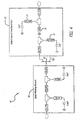
- Fig. 1a is a simplified schematic diagram of an ideal discrete component implementation of a typical Class-E load in accordance with conventional teachings.
- a typical Class-E amplifier represented by a switch 12' is coupled to a source V ds via an inductive bias line 14'.
- the switch 12' is coupled to a resistive load 24' via a capacitor 22' and an inverted L type (series L, shunt C) wave shaping load network 20'.
- the drain bias line 14' is treated independent of the load circuit 20', merely acting as a choke realized by a quarter wavelength length of transmission line.
- the load 20' includes a first shunt capacitor 15' which is the drain to source capacitance (C ds ) of the transistor switch 12'.
- the load 20' includes a series inductor 16' (L) and a shunt capacitor 18' (C).
- Fig. 1b is a distributed component implementation of the load depicted in Fig. 1a .
- the function of the load network in the class E amplifier is to shape the voltage and current waveforms. Therefore, for the design of a broadband Class-E amplifier, care should be taken to ensure Class-E waveforms exist over the entire frequency band.
- Choices of a suitable device non-linear modeling tool as well as a design environment tool capable of time domain, robust harmonic balance and envelope simulation are critical for the successful design of highly non-linear circuits such as the switching mode amplifiers.
- Fig. 2a is a simplified schematic diagram of an ideal discrete component implementation of a typical Class-E load in accordance with the teachings of the present invention.
- Fig. 2b is a distributed component implementation of the load depicted in Fig. 2a .
- a novel broadband Class-E load topology is presented based on the series (L-C) network shown in Fig. 2a .
- the load is modified to offer a superior broadband performance when compared with the (series L, shunt C) load network of Figs. 1a and 1b .
- the first step in the novel design process is to include the drain bias inductor 14 as part of the Class-E load topology followed by the transformation of the lumped network representation to its equivalent distributed network form.
- the series inductor 16 and series capacitor 18 of Fig. 2a are replaced by a combination of a series transmission line and a shunt shorted stub as shown in Fig 2b .
- the shunt inductor 14 of Fig. 2a is replaced with a shunt shorted stub to provide a parallel resonance with the pHEMT's output drain-source capacitance (Cds) as well as to provide a bias to the drain of the pHEMT transistor.
- a time domain simulation is performed to optimize the load with the objective of obtaining near ideal current and voltage waveforms over a desired operating range (e.g. 8 - 10 GHz).
- Fig. 2c shows these simulated waveforms illustrating near ideal performance over 2.0 GHz of bandwidth.
- the frequency dependency of the broadband lumped equivalent circuit representation of the load is shown in Fig. 3 (a) , depicting an excellent frequency independent response over 8.0-10.0 GHz compared to the narrowband Class-E load (series L, shunt C). See " A Monolithic X-band Class-E Power Amplifier", by R. Tayrani, IEEE GaAs IC Symposium, PP 205-208, Oct. 2001 .
- Figure 3b is a diagram which illustrates the time domain simulation of the distributed load network illustrating near ideal performance at 8 GHz. As shown in Figure 3b , the voltage waveform across the switch rises slowly at switch-off and falls to zero at the end of the half-cycle. It also has a zero rate of change at the end of half-cycle, thereby ensuring a "soft" turn-on condition.
- the load circuit is synthesized for medium power PAs ( ⁇ 30 dBm, 1.0 W max).
- a single 0.25 um x 720 um pHEMT device is used in this circuit.
- Such PAs are suitable as a single stage PA and/or as the first stage of a two stage Class-E High Power Amplifiers (HPAs).
- Figure 4 shows a schematic circuit of a distributed representation of a monolithic Class-E amplifier with the broadband Class-E load in accordance with the present teachings.
- the amplifier 30 of Fig. 4 includes an active device 12 with the inventive load 20.
- the active device 12 is a Gallium-Arsenide pseudo-morphic, high-electron mobility transistor (GaAs pHEMT).
- An input matching network 40 is provided at the input to the active device 12.
- the load 20 and input matching network 40 are designed with the width and length dimensions shown in microns for operation at 8 - 10 Ghz. Those of ordinary skill in the art may extend the present teachings to other frequencies without departing from the scope thereof.
- the device non-linear model should have the following properties:
- the device model should be able to accurately model the dispersion associated with the drain current, gm, and R ds . If the pulsed DC IV technique is used for the model development, this requirement may be unnecessary.
- the EEHEMT model available in ICCAP (Agilent ICCAP, V.5.1) and ADS (Agilent Advanced Design Systems (ADS), V. 2003C).
- a 0.3 ⁇ m x 6 x 120 ⁇ m pHEMT device having a gate-drain breakdown voltage of greater than 18 V may be designed using currently available technology in accordance with the present teachings to meet performance goals for very large (>100,000 T/R elements) space based phased array radar requiring simultaneous broadband power (min. 200.0 mW) and PAE (min. 60%) over 8.0 - 10.0 GHz.
- Figure 5 depicts simulated voltage and current waveforms at the pHEMT output terminals of the amplifier of Fig 4 .
- the waveforms show a switching mode behavior of the pHEMT device at 8.5 GHz. Similar waveforms may be provided over 8 - 10 GHz to confirm broadband operation.
- the present invention has been described herein with reference to a particular embodiment for a particular application. Those having ordinary skill in the art and access to the present teachings will recognize additional modifications applications and embodiments within the scope thereof.
- the present teachings are not limited to Class-E amplifiers. That is, the present teachings may be used in connection with any switching amplifier or circuit design.
Description
- The present invention relates to electrical and electronic circuits and systems. More specifically, the present invention relates to microwave Class E power amplifiers.
- For a variety of commercial and military applications, highly efficient microwave and radio frequency (RF) power amplifiers are needed. Typical applications include wireless local area networks, cell phones and telecommunication systems as well as advanced airborne active phased array radar systems. The choice of technology, design methodology and manufacturing cycle time are major cost contributors in these systems. Switching mode, Class-E, high-efficiency power amplifiers are useful for these and other applications inasmuch as these amplifiers limit the power and associated cooling costs thereof. A Class-E amplifier is part of the "switching mode amplifiers" such as class D, E, F, etc. In these types of amplifiers, the transistor operates as a perfect switch with no overlapping voltage & current waveforms at its output terminal, thereby ideally dissipating zero DC power. Other classes of amplifiers such as class A, A/B and C, operate as a current-source with overlapping voltage & current waveforms and hence dissipate DC power leading to a lower efficiency.
Class-E amplifiers, as described inUS 2004/0113689 A1 , use a series or parallel resonant load network. The function of the load network in the class-E amplifier is to shape the voltage and current waveforms. The current and voltage time-waveforms at the active device output terminal are optimized in such a way as to minimize the DC power dissipation within. The active device, a pHEMT in this case, acts as a switch, driven by the RF input signal to "ON" and "OFF" conditions. The operating point of the device is such that the device is either OFF (in the pinched-off region) or ON (in the linear region). Under an ideal switching operation condition, output voltage and current waveforms at the device output terminal do not exist simultaneously and, therefore, the energy dissipated within the device is zero, yielding a 100 percent theoretical power conversion efficiency. - Further, document
US 3 919 656 A shows another high-efficiency tuned switching power amplifier. - Everard, J.K.A.; WILKINSON, A.J.: "Transmission-line load-network topology for class-E power amplifiers"; MICROWAVE THEORY AND TECHNIQUES, IEEE TRANSACTIONS ON, vol. 49, no. 6, 30 June 2001 (2001-06-30), pages 1202-1210, XP002571194, discloses a topology and design methodology which could be used for a transmission-line implementation of a class-E power amplifier.
- In any event, the maximum efficiency of Class-E amplifiers (i.e. the ratio of the RF output power to the DC input power) and its bandwidth of operation are limited by the tuned loads thereof. The limitation is due to the fact that presence of the tuned load results in a very narrow operational bandwidth for the amplifier.
- Hence, a need remains in the art for a system or method for increasing the power, power added efficiency (PAE) and bandwidth of Class-E amplifiers.
- The need in the art is addressed by a method for designing a load for use with a class-E amplifier having a transistor switch, including the steps of: providing a lumped equivalent circuit representation of the load, including a shunt capacitor (15) which is the drain to source capacitance (Cds) of the transistor switch (12), and including a drain bias inductor as a part of the Class-E load topology; optimizing the lumped equivalent circuit representation of the load to achieve near ideal current and voltage operational characteristics over a predetermined frequency range using a time domain simulation; transforming the optimized lumped equivalent circuit representation of the load to a distributed circuit representation wherein the drain bias inductor is replaced with a shunt shorted stub to provide a parallel resonance with the drain to source capacitance as well as to provide a bias to the drain of the transistor switch; and optimizing the distributed circuit representation of the load to achieve near ideal current and voltage operational characteristics over a predetermined frequency range using a time domain simulation.
- Load circuit topologies designed according to the present invention are suitable for switching mode Power Amplifiers (PAs). In a most general sense, the designed load includes a shunt inductive element coupled to an output of said amplifier; a series inductive element coupled to said output of said amplifier; and a series capacitive element coupled to said series inductive element.
- In the illustrative embodiment, the designed load is operable at frequencies in the range of 8 - 10 GHz and beyond. The shunt inductive element, part of the said load is suitably chosen to provide two important functions. First, to provide an inductive bias line for said amplifier and second, to provide a parallel resonance with the pHEMT's output drain-source capacitance (Cds).
- The invention enables an advantageous class-E amplifier design comprising an input matching network; an active device coupled to the input matching network and a load coupled to the active device and implemented in accordance with the present teachings.
- The unique properties of the inventive load circuits enable Class-E HPAs to maintain a simultaneous high PAE and Power over a broad bandwidth.
-
-
Fig. 1a is a simplified schematic diagram of an ideal discrete component implementation of a typical Class-E load in accordance with conventional teachings. -
Fig. 1b is a distributed component implementation of the load depicted inFig. 1a . -
Fig. 2a is a simplified schematic diagram of an ideal discrete component implementation of a typical Class-E load in accordance with the teachings of the present invention. -
Fig. 2b is a distributed component implementation of the load depicted inFig. 2a . -
Fig. 2c shows graphs of current and voltage waveforms of a lumped equivalent circuit representation of the load designed in accordance with the present teachings. -
Fig. 3 a is a Smith chart showing frequency dependency of a broadband lumped load designed in accordance with the teachings of the present invention. -
Figure 4 shows a schematic circuit of a distributed representation of a monolithic Class-E amplifier with the broadband Class-E load in accordance with the present teachings. -
Figure 5 depicts simulated voltage and current waveforms at the pHEMT output terminals of the amplifier ofFig 4 . - Illustrative embodiments and exemplary applications will now be described with reference to the accompanying drawings to disclose the advantageous teachings of the present invention.
- While the present invention is described herein with reference to illustrative embodiments for particular applications, it should be understood that the invention is not limited thereto. Those having ordinary skill in the art and access to the teachings provided herein will recognize additional modifications, applications, and embodiments within the scope thereof and additional fields in which the present invention would be of significant utility.
-
Fig. 1a is a simplified schematic diagram of an ideal discrete component implementation of a typical Class-E load in accordance with conventional teachings. As shown inFig. 1a , a typical Class-E amplifier represented by a switch 12' is coupled to a source Vds via an inductive bias line 14'. The switch 12' is coupled to a resistive load 24' via a capacitor 22' and an inverted L type (series L, shunt C) wave shaping load network 20'. The drain bias line 14' is treated independent of the load circuit 20', merely acting as a choke realized by a quarter wavelength length of transmission line. - The load 20' includes a first shunt capacitor 15' which is the drain to source capacitance (Cds) of the transistor switch 12'. In accordance with conventional teachings, the load 20' includes a series inductor 16' (L) and a shunt capacitor 18' (C).
-
Fig. 1b is a distributed component implementation of the load depicted inFig. 1a . It is worth mentioning that the function of the load network in the class E amplifier is to shape the voltage and current waveforms. Therefore, for the design of a broadband Class-E amplifier, care should be taken to ensure Class-E waveforms exist over the entire frequency band. Choices of a suitable device non-linear modeling tool as well as a design environment tool capable of time domain, robust harmonic balance and envelope simulation are critical for the successful design of highly non-linear circuits such as the switching mode amplifiers. -
Fig. 2a is a simplified schematic diagram of an ideal discrete component implementation of a typical Class-E load in accordance with the teachings of the present invention. -
Fig. 2b is a distributed component implementation of the load depicted inFig. 2a . In accordance with the present teachings, a novel broadband Class-E load topology is presented based on the series (L-C) network shown inFig. 2a . As discussed more fully below, the load is modified to offer a superior broadband performance when compared with the (series L, shunt C) load network ofFigs. 1a and 1b . In accordance with the present teachings, the first step in the novel design process is to include thedrain bias inductor 14 as part of the Class-E load topology followed by the transformation of the lumped network representation to its equivalent distributed network form. In this critical transformation process which is necessary for the said amplifier to operate at microwave frequencies, theseries inductor 16 andseries capacitor 18 ofFig. 2a are replaced by a combination of a series transmission line and a shunt shorted stub as shown inFig 2b . Also, theshunt inductor 14 ofFig. 2a is replaced with a shunt shorted stub to provide a parallel resonance with the pHEMT's output drain-source capacitance (Cds) as well as to provide a bias to the drain of the pHEMT transistor. - Next, starting values for the lumped components of the
load network 20 are ascertained. Several authors have published detailed expressions for the starting values of the lumped series (L, C) Class-E load. See for example "Class-E - A new class of high efficiency tuned single-ended switching power amplifier", by N. O. Sokal, et al. IEEEE JSSC, vol. SSC-10, pp.168-176, June 1975; "Solid State Radio Engineering" by F. H. Raab, et al., John Wiley & Sons, 1980; "Low Voltage, High Efficiency Class E GaAs Power Amplifiers for Mobile Communications", by T. Sowlati, et al. IEEE GaAs IC Symposium Digest 1994, pp.171-174; "Switched-Mode High-Efficiency Microwave Power Amplifiers In A Free-Space Power Combiner", by T. Mader, et al., IEEE MTT, vol. 10. Oct. 1998, pp. 1391-1398; and " Ultra-High Efficiency Operation Based On An Alternative Class-E Mode", P. Watson, et al., IEEE GaAs IC Symposium Digest 2000, pp.53-56. - Next, having obtained the starting values for the load network, a time domain simulation is performed to optimize the load with the objective of obtaining near ideal current and voltage waveforms over a desired operating range (e.g. 8 - 10 GHz).
-
Fig. 2c shows these simulated waveforms illustrating near ideal performance over 2.0 GHz of bandwidth. The frequency dependency of the broadband lumped equivalent circuit representation of the load is shown inFig. 3 (a) , depicting an excellent frequency independent response over 8.0-10.0 GHz compared to the narrowband Class-E load (series L, shunt C). See "A Monolithic X-band Class-E Power Amplifier", by R. Tayrani, IEEE GaAs IC Symposium, PP 205-208, Oct. 2001. - Having obtained a nearly frequency independent magnitude and phase response for the lumped equivalent circuit representation of the load network, we can now proceed to the next step by transforming this load to its equivalent distributed network. (See
Fig. 2b .) - To optimize the distributed load, the time domain optimization process described for the lumped load is repeated for the distributed load.
-
Figure 3b is a diagram which illustrates the time domain simulation of the distributed load network illustrating near ideal performance at 8 GHz. As shown inFigure 3b , the voltage waveform across the switch rises slowly at switch-off and falls to zero at the end of the half-cycle. It also has a zero rate of change at the end of half-cycle, thereby ensuring a "soft" turn-on condition. - Furthermore, it is shown that the integral of the capacitor (Cds) current over the half-cycle is zero and that the capacitance current has dropped to zero by the end of the half-cycle, both indicative of Class-E operation for the distributed load at 8.0 GHz. Similar simulated waveforms were obtained over the desired 2.0 GHz frequency band. Although not shown, the frequency response of the distributed load (
Figure 2b ) should also be broadband having a nearly frequency independent response similar to its lumped version shown inFigure 3 (a) . - In the illustrative application, the load circuit is synthesized for medium power PAs (∼ 30 dBm, 1.0 W max). A single 0.25 um x 720 um pHEMT device is used in this circuit. Such PAs are suitable as a single stage PA and/or as the first stage of a two stage Class-E High Power Amplifiers (HPAs).
-
Figure 4 shows a schematic circuit of a distributed representation of a monolithic Class-E amplifier with the broadband Class-E load in accordance with the present teachings. Theamplifier 30 ofFig. 4 includes anactive device 12 with theinventive load 20. In the illustrative embodiment, theactive device 12 is a Gallium-Arsenide pseudo-morphic, high-electron mobility transistor (GaAs pHEMT). - An
input matching network 40 is provided at the input to theactive device 12. Theload 20 andinput matching network 40 are designed with the width and length dimensions shown in microns for operation at 8 - 10 Ghz. Those of ordinary skill in the art may extend the present teachings to other frequencies without departing from the scope thereof. - For accurate and robust non-linear simulation of switching mode amplifiers, the device non-linear model should have the following properties:
- Bias dependency of drain-to-source Cds(Vds,Vgs) and gate-to-drain Cgd (Vds,Vgs) capacitances;
- Bias dependency of input channel resistance Ri(Vds,Vgs); and
- Bias dependency of output channel resistance Rds(Vds,Vgs).
- Also the device model should be able to accurately model the dispersion associated with the drain current, gm, and Rds. If the pulsed DC IV technique is used for the model development, this requirement may be unnecessary. For this purpose, the EEHEMT model available in ICCAP (Agilent ICCAP, V.5.1) and ADS (Agilent Advanced Design Systems (ADS), V. 2003C).
- A 0.3 µm x 6 x 120 µm pHEMT device having a gate-drain breakdown voltage of greater than 18 V may be designed using currently available technology in accordance with the present teachings to meet performance goals for very large (>100,000 T/R elements) space based phased array radar requiring simultaneous broadband power (min. 200.0 mW) and PAE (min. 60%) over 8.0 - 10.0 GHz.
-
Figure 5 depicts simulated voltage and current waveforms at the pHEMT output terminals of the amplifier ofFig 4 . The waveforms show a switching mode behavior of the pHEMT device at 8.5 GHz. Similar waveforms may be provided over 8 - 10 GHz to confirm broadband operation. - Thus, the present invention has been described herein with reference to a particular embodiment for a particular application. Those having ordinary skill in the art and access to the present teachings will recognize additional modifications applications and embodiments within the scope thereof. For example, the present teachings are not limited to Class-E amplifiers. That is, the present teachings may be used in connection with any switching amplifier or circuit design.
- It is therefore intended by the appended claims to cover any and all such applications, modifications and embodiments within the scope of the present invention.
Claims (1)
- Method for designing a load (20) for use with a Class-E amplifier (30) having a transistor switch (12), including the steps of:providing a lumped equivalent circuit representation of the load (20), including a shunt capacitor (15) which is the drain to source capacitance (Cd5) of the transistor switch (12), and including a drain bias inductor (14) as a part of the Class-E load topology (20);optimizing at the lumped equivalent circuit representation of the load (20) to achieve near ideal current and voltage operational characteristics over a predetermined frequency range using a time domain simulation;transforming the optimized lumped equivalent circuit representation of the load (20) to a distributed circuit representation wherein the drain bias inductor (14) is replaced with a shunt shorted stub to provide a parallel resonance with the drain to source capacitance (Cds) as well as to provide a bias to the drain of the transistor switch (12); andoptimizing the distributed circuit representation of the load (20) to achieve near ideal current and voltage operational characteristics over a predetermined frequency range using a time domain simulation.
Applications Claiming Priority (2)
| Application Number | Priority Date | Filing Date | Title |
|---|---|---|---|
| US11/054,968 US7345539B2 (en) | 2005-02-10 | 2005-02-10 | Broadband microwave amplifier |
| EP06720546A EP1849232A1 (en) | 2005-02-10 | 2006-02-09 | Broadband microwave amplifier |
Related Parent Applications (1)
| Application Number | Title | Priority Date | Filing Date |
|---|---|---|---|
| EP06720546.8 Division | 2006-02-09 |
Publications (2)
| Publication Number | Publication Date |
|---|---|
| EP2182632A1 EP2182632A1 (en) | 2010-05-05 |
| EP2182632B1 true EP2182632B1 (en) | 2013-01-02 |
Family
ID=36499224
Family Applications (2)
| Application Number | Title | Priority Date | Filing Date |
|---|---|---|---|
| EP10152522A Active EP2182632B1 (en) | 2005-02-10 | 2006-02-09 | Broadband microwave amplifier |
| EP06720546A Withdrawn EP1849232A1 (en) | 2005-02-10 | 2006-02-09 | Broadband microwave amplifier |
Family Applications After (1)
| Application Number | Title | Priority Date | Filing Date |
|---|---|---|---|
| EP06720546A Withdrawn EP1849232A1 (en) | 2005-02-10 | 2006-02-09 | Broadband microwave amplifier |
Country Status (8)
| Country | Link |
|---|---|
| US (1) | US7345539B2 (en) |
| EP (2) | EP2182632B1 (en) |
| JP (2) | JP2008530910A (en) |
| KR (1) | KR20070096015A (en) |
| CA (1) | CA2577791C (en) |
| DK (1) | DK2182632T3 (en) |
| NO (2) | NO20074547L (en) |
| WO (1) | WO2006086542A1 (en) |
Cited By (1)
| Publication number | Priority date | Publication date | Assignee | Title |
|---|---|---|---|---|
| CN107547050A (en) * | 2017-08-21 | 2018-01-05 | 天津大学 | A kind of twin-stage double frequency-band high efficiency power amplifier |
Families Citing this family (8)
| Publication number | Priority date | Publication date | Assignee | Title |
|---|---|---|---|---|
| JP5419812B2 (en) * | 2010-06-30 | 2014-02-19 | 三菱電機株式会社 | High-frequency multistage active circuit |
| FR2965082B1 (en) | 2010-09-21 | 2012-09-28 | Inside Contactless | METHOD AND DEVICE FOR INDUCTIVE COUPLING ACTIVATED LOAD MODULATION |
| JP5759286B2 (en) * | 2011-06-27 | 2015-08-05 | 住友電気工業株式会社 | Switching circuit |
| US9083291B2 (en) | 2011-08-12 | 2015-07-14 | Bae Systems Information And Electronic Systems Integration Inc. | Low voltage high efficiency gallium arsenide power amplifier |
| US8456238B1 (en) | 2012-03-30 | 2013-06-04 | Centellax, Inc. | Tapered attenuator network for mitigating effects of direct current (DC) bias inductor self-resonance in traveling wave amplifiers |
| JP6049673B2 (en) * | 2014-10-31 | 2016-12-21 | 株式会社東芝 | Semiconductor amplifier |
| CN105550790B (en) * | 2016-03-08 | 2019-08-06 | 重庆大学 | Interconnected network idle work optimization calculation method based on non-topological approach equivalence |
| CN111985177B (en) * | 2020-06-30 | 2023-05-02 | 宁波大学 | Design method of radio frequency power amplifier |
Family Cites Families (22)
| Publication number | Priority date | Publication date | Assignee | Title |
|---|---|---|---|---|
| US3919656A (en) | 1973-04-23 | 1975-11-11 | Nathan O Sokal | High-efficiency tuned switching power amplifier |
| JPS59814Y2 (en) * | 1977-04-22 | 1984-01-11 | ブライアン・ア−ネスト・アトウツド | class D amplifier |
| US4717884A (en) * | 1986-04-14 | 1988-01-05 | Motorola, Inc. | High efficiency RF power amplifier |
| US4763087A (en) | 1986-05-27 | 1988-08-09 | Schrader Paul D | Impedance matching network |
| JPS63279608A (en) * | 1987-05-11 | 1988-11-16 | Nippon Telegr & Teleph Corp <Ntt> | Integrated amplifier circuit |
| JPH0732335B2 (en) | 1990-11-16 | 1995-04-10 | 日本電信電話株式会社 | High frequency amplifier |
| DE69221716T2 (en) * | 1991-02-04 | 1997-12-18 | Advanced Energy Ind Inc | Method and device for switching high-performance radio frequency amplification |
| JPH0554094A (en) * | 1991-08-23 | 1993-03-05 | Mitsubishi Electric Corp | Circuit simulation device |
| JP2627113B2 (en) * | 1992-01-16 | 1997-07-02 | 岩崎通信機株式会社 | High frequency power amplifier |
| JPH06196902A (en) * | 1992-12-25 | 1994-07-15 | Akira Ogawa | Band pass filter |
| US6121840A (en) * | 1996-12-24 | 2000-09-19 | Murata Manufacturing Co., Ltd. | High-frequency amplifier |
| JP4157619B2 (en) * | 1997-09-24 | 2008-10-01 | 東芝キヤリア株式会社 | Air conditioner |
| JP2000165175A (en) | 1998-11-27 | 2000-06-16 | Kyosan Electric Mfg Co Ltd | Impedance matching device |
| JP2000341162A (en) * | 1999-05-31 | 2000-12-08 | Debon Multimedia Kk | Shared unit branching and combining two carriers with different frequencies and method for propagating two carriers with difference frequency utilizing the shared unit |
| US6232841B1 (en) | 1999-07-01 | 2001-05-15 | Rockwell Science Center, Llc | Integrated tunable high efficiency power amplifier |
| US6469919B1 (en) * | 1999-07-22 | 2002-10-22 | Eni Technology, Inc. | Power supplies having protection circuits |
| CN1295865C (en) | 2000-10-10 | 2007-01-17 | 加利福尼亚技术协会 | Class E/F switching power amplifiers |
| US6603352B2 (en) * | 2001-12-03 | 2003-08-05 | Icefyre Semiconductor Corporation | Switched-mode power amplifier integrally performing power combining |
| US6552610B1 (en) * | 2002-01-15 | 2003-04-22 | Mva.Com Eurotec, B.V. | Transmission-line tuned switching power amplifier |
| US6806767B2 (en) * | 2002-07-09 | 2004-10-19 | Anadigics, Inc. | Power amplifier with load switching circuit |
| US20040027209A1 (en) | 2002-08-09 | 2004-02-12 | Applied Materials, Inc. | Fixed matching network with increased match range capabilities |
| US6949978B2 (en) * | 2003-10-17 | 2005-09-27 | Raytheon Company | Efficient broadband switching-mode amplifier |
-
2005
- 2005-02-10 US US11/054,968 patent/US7345539B2/en active Active
-
2006
- 2006-02-09 WO PCT/US2006/004554 patent/WO2006086542A1/en active Application Filing
- 2006-02-09 JP JP2007555213A patent/JP2008530910A/en not_active Withdrawn
- 2006-02-09 CA CA2577791A patent/CA2577791C/en active Active
- 2006-02-09 EP EP10152522A patent/EP2182632B1/en active Active
- 2006-02-09 EP EP06720546A patent/EP1849232A1/en not_active Withdrawn
- 2006-02-09 KR KR1020077018416A patent/KR20070096015A/en not_active Application Discontinuation
- 2006-02-09 DK DK10152522.8T patent/DK2182632T3/en active
-
2007
- 2007-09-07 NO NO20074547A patent/NO20074547L/en not_active Application Discontinuation
-
2012
- 2012-06-21 JP JP2012139986A patent/JP5362884B2/en not_active Expired - Fee Related
-
2017
- 2017-01-16 NO NO20170060A patent/NO340987B1/en unknown
Cited By (2)
| Publication number | Priority date | Publication date | Assignee | Title |
|---|---|---|---|---|
| CN107547050A (en) * | 2017-08-21 | 2018-01-05 | 天津大学 | A kind of twin-stage double frequency-band high efficiency power amplifier |
| CN107547050B (en) * | 2017-08-21 | 2020-12-15 | 天津大学 | Two-stage dual-band high-efficiency power amplifier |
Also Published As
| Publication number | Publication date |
|---|---|
| NO20074547L (en) | 2007-10-29 |
| NO20170060A1 (en) | 2017-01-16 |
| CA2577791C (en) | 2010-11-23 |
| WO2006086542A1 (en) | 2006-08-17 |
| NO340987B1 (en) | 2017-07-31 |
| KR20070096015A (en) | 2007-10-01 |
| JP2008530910A (en) | 2008-08-07 |
| DK2182632T3 (en) | 2013-03-25 |
| EP2182632A1 (en) | 2010-05-05 |
| CA2577791A1 (en) | 2006-08-17 |
| JP5362884B2 (en) | 2013-12-11 |
| EP1849232A1 (en) | 2007-10-31 |
| JP2012231506A (en) | 2012-11-22 |
| US20060176114A1 (en) | 2006-08-10 |
| US7345539B2 (en) | 2008-03-18 |
Similar Documents
| Publication | Publication Date | Title |
|---|---|---|
| EP2182632B1 (en) | Broadband microwave amplifier | |
| EP1911155B1 (en) | Two stage microwave class e power amplifier | |
| Song et al. | A CMOS class-E power amplifier with voltage stress relief and enhanced efficiency | |
| Lee et al. | A CMOS outphasing power amplifier with integrated single-ended Chireix combiner | |
| Meshkin et al. | A novel 2.4 GHz CMOS class-E power amplifier with efficient power control for wireless communications | |
| Gao et al. | Two-stage quasi-class-E power amplifier in GaN HEMT technology | |
| Zarghami et al. | A novel design methodology for extended continuous class-F power amplifiers in wireless applications | |
| Lin et al. | Development of a wideband highly efficient GaN VMCD VHF/UHF power amplifier | |
| Moon et al. | A multimode/multiband envelope tracking transmitter with broadband saturated power amplifier | |
| Tayrani | A broadband monolithic S-band class-E power amplifier | |
| Khan et al. | Design of a broadband current mode class-D power amplifier with harmonic suppression | |
| Liu et al. | A class-E RF power amplifier with a novel matching network for high-efficiency dynamic load modulation | |
| Hammi et al. | Comparative study of recent advances in power amplification devices and circuits for wireless communication infrastructure | |
| Tayrani | A highly efficient broadband (7-14 GHz) monolithic class e power amplifier for space based radar | |
| Khan et al. | A parallel circuit differential class-E power amplifier using series capacitance | |
| Dehqan et al. | Resonance gate bias cascode class-E power amplifier in GaAs pHEMT technology | |
| Khaleel | Design of class-E Power Amplifier (PA) with minimum harmonious termination for Cellular phones | |
| Mesquita et al. | High-efficiency watt-level MASMOS® power amplifier for LTE applications | |
| CN112653405A (en) | Wideband power amplifier and method of construction thereof | |
| KIRISH | DESIGN OF DUAL-BAND MATCHING NETWORK FOR HIGHLY EFFICIENT POWER AMPLIFIER. | |
| Aruna et al. | Efficiency enchancement of Class-E power amplifier in VHF radio frequency spectrum for land mobile radio system | |
| Shukla et al. | A Comparative Analysis between GaN-Based Current and Voltage Mode Class-D and E PAs for Communications | |
| Panda et al. | An Efficient And Power Optimized Cascode Stage RF Tuned Class-E Power Amplifier | |
| Aflaki et al. | 1 GHz current mode class-D power amplifier in hybrid technology using GaN HEMTs | |
| Popovic et al. | Efficient X-band switched-mode microwave power amplifiers |
Legal Events
| Date | Code | Title | Description |
|---|---|---|---|
| PUAI | Public reference made under article 153(3) epc to a published international application that has entered the european phase |
Free format text: ORIGINAL CODE: 0009012 |
|
| 17P | Request for examination filed |
Effective date: 20100203 |
|
| AC | Divisional application: reference to earlier application |
Ref document number: 1849232 Country of ref document: EP Kind code of ref document: P |
|
| AK | Designated contracting states |
Kind code of ref document: A1 Designated state(s): DE DK FR IT NL SE |
|
| RBV | Designated contracting states (corrected) |
Designated state(s): AT BE BG CH CY CZ DE DK EE ES FI FR GB GR HU IE IS IT LI LT LU LV MC NL PL PT RO SE SI SK TR |
|
| 17Q | First examination report despatched |
Effective date: 20100723 |
|
| REG | Reference to a national code |
Ref country code: DE Ref legal event code: R079 Ref document number: 602006034051 Country of ref document: DE Free format text: PREVIOUS MAIN CLASS: H03F0003217000 Ipc: H03H0007380000 |
|
| GRAP | Despatch of communication of intention to grant a patent |
Free format text: ORIGINAL CODE: EPIDOSNIGR1 |
|
| RIC1 | Information provided on ipc code assigned before grant |
Ipc: H03H 7/38 20060101AFI20120627BHEP Ipc: H03F 3/217 20060101ALI20120627BHEP |
|
| RBV | Designated contracting states (corrected) |
Designated state(s): DE DK FR IT NL SE |
|
| GRAS | Grant fee paid |
Free format text: ORIGINAL CODE: EPIDOSNIGR3 |
|
| GRAA | (expected) grant |
Free format text: ORIGINAL CODE: 0009210 |
|
| AC | Divisional application: reference to earlier application |
Ref document number: 1849232 Country of ref document: EP Kind code of ref document: P |
|
| AK | Designated contracting states |
Kind code of ref document: B1 Designated state(s): DE DK FR IT NL SE |
|
| REG | Reference to a national code |
Ref country code: SE Ref legal event code: TRGR |
|
| REG | Reference to a national code |
Ref country code: DE Ref legal event code: R096 Ref document number: 602006034051 Country of ref document: DE Effective date: 20130228 |
|
| REG | Reference to a national code |
Ref country code: DK Ref legal event code: T3 |
|
| REG | Reference to a national code |
Ref country code: NL Ref legal event code: T3 |
|
| PLBE | No opposition filed within time limit |
Free format text: ORIGINAL CODE: 0009261 |
|
| STAA | Information on the status of an ep patent application or granted ep patent |
Free format text: STATUS: NO OPPOSITION FILED WITHIN TIME LIMIT |
|
| 26N | No opposition filed |
Effective date: 20131003 |
|
| REG | Reference to a national code |
Ref country code: DE Ref legal event code: R097 Ref document number: 602006034051 Country of ref document: DE Effective date: 20131003 |
|
| REG | Reference to a national code |
Ref country code: FR Ref legal event code: PLFP Year of fee payment: 11 |
|
| REG | Reference to a national code |
Ref country code: FR Ref legal event code: PLFP Year of fee payment: 12 |
|
| REG | Reference to a national code |
Ref country code: FR Ref legal event code: PLFP Year of fee payment: 13 |
|
| PGFP | Annual fee paid to national office [announced via postgrant information from national office to epo] |
Ref country code: SE Payment date: 20220120 Year of fee payment: 17 |
|
| PGFP | Annual fee paid to national office [announced via postgrant information from national office to epo] |
Ref country code: FR Payment date: 20230119 Year of fee payment: 18 Ref country code: DK Payment date: 20230119 Year of fee payment: 18 |
|
| PGFP | Annual fee paid to national office [announced via postgrant information from national office to epo] |
Ref country code: IT Payment date: 20230120 Year of fee payment: 18 Ref country code: DE Payment date: 20230119 Year of fee payment: 18 |
|
| PGFP | Annual fee paid to national office [announced via postgrant information from national office to epo] |
Ref country code: NL Payment date: 20230119 Year of fee payment: 18 |
|
| REG | Reference to a national code |
Ref country code: SE Ref legal event code: EUG |
|
| PG25 | Lapsed in a contracting state [announced via postgrant information from national office to epo] |
Ref country code: SE Free format text: LAPSE BECAUSE OF NON-PAYMENT OF DUE FEES Effective date: 20230210 |