EP2177879B1 - Drehmelderschnittstelle und Signalformer - Google Patents
Drehmelderschnittstelle und Signalformer Download PDFInfo
- Publication number
- EP2177879B1 EP2177879B1 EP09251431.4A EP09251431A EP2177879B1 EP 2177879 B1 EP2177879 B1 EP 2177879B1 EP 09251431 A EP09251431 A EP 09251431A EP 2177879 B1 EP2177879 B1 EP 2177879B1
- Authority
- EP
- European Patent Office
- Prior art keywords
- sine
- cosine
- input
- resolver
- excitation
- Prior art date
- Legal status (The legal status is an assumption and is not a legal conclusion. Google has not performed a legal analysis and makes no representation as to the accuracy of the status listed.)
- Active
Links
- 230000005284 excitation Effects 0.000 claims description 55
- 238000004364 calculation method Methods 0.000 claims description 13
- 238000005070 sampling Methods 0.000 claims description 10
- 238000000034 method Methods 0.000 claims description 9
- 238000001914 filtration Methods 0.000 claims description 7
- 230000001360 synchronised effect Effects 0.000 claims description 7
- 230000009977 dual effect Effects 0.000 claims description 2
- 238000012545 processing Methods 0.000 claims description 2
- 238000012544 monitoring process Methods 0.000 claims 1
- 230000003750 conditioning effect Effects 0.000 description 6
- 230000006870 function Effects 0.000 description 5
- 238000010586 diagram Methods 0.000 description 3
- 230000010363 phase shift Effects 0.000 description 3
- 238000012360 testing method Methods 0.000 description 3
- 239000000872 buffer Substances 0.000 description 2
- 238000004422 calculation algorithm Methods 0.000 description 2
- 230000015556 catabolic process Effects 0.000 description 2
- 238000006731 degradation reaction Methods 0.000 description 2
- 230000007257 malfunction Effects 0.000 description 2
- 230000008569 process Effects 0.000 description 2
- 230000004044 response Effects 0.000 description 2
- 239000013598 vector Substances 0.000 description 2
- 230000002411 adverse Effects 0.000 description 1
- 230000008859 change Effects 0.000 description 1
- 230000001143 conditioned effect Effects 0.000 description 1
- 238000012790 confirmation Methods 0.000 description 1
- 230000001419 dependent effect Effects 0.000 description 1
- 238000013461 design Methods 0.000 description 1
- 230000004069 differentiation Effects 0.000 description 1
- 238000006073 displacement reaction Methods 0.000 description 1
- 230000000694 effects Effects 0.000 description 1
- 230000036541 health Effects 0.000 description 1
- 238000012986 modification Methods 0.000 description 1
- 230000004048 modification Effects 0.000 description 1
- 230000003287 optical effect Effects 0.000 description 1
- 239000004065 semiconductor Substances 0.000 description 1
- 238000012163 sequencing technique Methods 0.000 description 1
- 230000009466 transformation Effects 0.000 description 1
Images

Classifications
-
- G—PHYSICS
- G01—MEASURING; TESTING
- G01D—MEASURING NOT SPECIALLY ADAPTED FOR A SPECIFIC VARIABLE; ARRANGEMENTS FOR MEASURING TWO OR MORE VARIABLES NOT COVERED IN A SINGLE OTHER SUBCLASS; TARIFF METERING APPARATUS; MEASURING OR TESTING NOT OTHERWISE PROVIDED FOR
- G01D5/00—Mechanical means for transferring the output of a sensing member; Means for converting the output of a sensing member to another variable where the form or nature of the sensing member does not constrain the means for converting; Transducers not specially adapted for a specific variable
- G01D5/12—Mechanical means for transferring the output of a sensing member; Means for converting the output of a sensing member to another variable where the form or nature of the sensing member does not constrain the means for converting; Transducers not specially adapted for a specific variable using electric or magnetic means
- G01D5/14—Mechanical means for transferring the output of a sensing member; Means for converting the output of a sensing member to another variable where the form or nature of the sensing member does not constrain the means for converting; Transducers not specially adapted for a specific variable using electric or magnetic means influencing the magnitude of a current or voltage
- G01D5/20—Mechanical means for transferring the output of a sensing member; Means for converting the output of a sensing member to another variable where the form or nature of the sensing member does not constrain the means for converting; Transducers not specially adapted for a specific variable using electric or magnetic means influencing the magnitude of a current or voltage by varying inductance, e.g. by a movable armature
- G01D5/22—Mechanical means for transferring the output of a sensing member; Means for converting the output of a sensing member to another variable where the form or nature of the sensing member does not constrain the means for converting; Transducers not specially adapted for a specific variable using electric or magnetic means influencing the magnitude of a current or voltage by varying inductance, e.g. by a movable armature differentially influencing two coils
- G01D5/2291—Linear or rotary variable differential transformers (LVDTs/RVDTs) having a single primary coil and two secondary coils
-
- H—ELECTRICITY
- H03—ELECTRONIC CIRCUITRY
- H03M—CODING; DECODING; CODE CONVERSION IN GENERAL
- H03M1/00—Analogue/digital conversion; Digital/analogue conversion
- H03M1/12—Analogue/digital converters
- H03M1/1205—Multiplexed conversion systems
- H03M1/122—Shared using a single converter or a part thereof for multiple channels, e.g. a residue amplifier for multiple stages
- H03M1/1225—Shared using a single converter or a part thereof for multiple channels, e.g. a residue amplifier for multiple stages using time-division multiplexing
-
- H—ELECTRICITY
- H03—ELECTRONIC CIRCUITRY
- H03M—CODING; DECODING; CODE CONVERSION IN GENERAL
- H03M1/00—Analogue/digital conversion; Digital/analogue conversion
- H03M1/12—Analogue/digital converters
- H03M1/64—Analogue/digital converters with intermediate conversion to phase of sinusoidal or similar periodical signals
- H03M1/645—Analogue/digital converters with intermediate conversion to phase of sinusoidal or similar periodical signals for position encoding, e.g. using resolvers or synchros
Definitions
- This disclosure generally relates to an interface and method of conditioning signals from a positional measuring device. More particularly, this disclosure relates to a resolver interface and method for conditioning signals from the resolver for improving accuracy of the resolver interface.
- a resolver is utilized for measuring and communicating a rotational position of a rotating member such as for example a motor shaft. The rotational position of a rotating member is communicated to provide for accurate control and operation.
- a conventional resolver provides a raw analog signal that is conditioned to generate a signal in a desired form.
- An interface including software and electronic hardware is utilized to condition signals received from the resolver and produce a signal in a desired form. The accuracy of the position measured is dependent not only on the resolver itself but also on the robustness of the interface utilized to condition resolver output signals.
- EP 1884746 discloses a signal conditioning circuit with time share multiplexers and a resolver.
- EP 0215724 discloses analog signal conditioning interfaces for conditioning AC displacement sensor analog information.
- a resolver interface includes separate anti-aliasing filters for sine cosine and excitation signals.
- the separately filtered signals are then time share multiplexed to a single analog to digital (A/D) converter. Because all of the inputs are fed through the same A/D converter, any error, difference or shift caused by the A/D converter is shared across all inputs.
- A/D analog to digital
- the A/D converter is controlled according to a control algorithm provided by a field programmable gate array (FPGA).
- the FPGA includes a sine wave generator that produces the excitation signal.
- the signals from the A/D converter are fed through digital filters in the FPGA. Because the digital filter is part of the FPGA each of the digital filters can be of an identical configuration, thereby eliminating any inherent inaccuracies potentially present with separate components.
- the digital demodulation calculations are synchronized with the resolver excitation frequency as both are performed by the FPGA.
- a "sliding" sine/cosine look up table keeps the table synchronized to the excitations phase and update rate in order to provide a correct indication of the quadrant of the phase results for each data update.
- the disclosed example resolver interface provides improved accuracy by reducing points of error or differentiation between signals from the initial filter to final calculations.
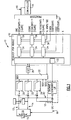
- a resolver interface and signal conditioner 10 is schematically shown and receives a sine input 12 and a cosine input 14 from a resolver 16.
- the sine input 12 and the cosine input 14 provide an analog signal indicative of a position of a rotary device 15 for four-quadrant accuracy and operation.
- the resolver interface 10 converts the analog signals 12, 14 into a four-quadrant angular position of the rotary device 15.
- the converted angular position is then communicated to a controller 44 or other device that utilizes the rotational position information.
- the disclosed example is a resolver interface, one skilled in the art would recognize the benefits applicable to other known differential position sensors such as for example a linear variable differential transformer (LVDT) and a rotary variable differential transformer (RVDT).
- LVDT linear variable differential transformer
- RVDT rotary variable differential transformer
- the resolver 16 receives an excitation signal 18 that provides for the generation of the sine input 12 and cosine input 14 to the resolver interface 10.
- the sine input 12 is fed through a first anti-aliasing filter 20.
- the cosine input 14 is fed through a second anti-aliasing filter 22.
- the excitation signal 18 can optionally be fed by way of an external or internal path through a third anti-aliasing filter 24.
- the filtered signals from the anti-aliasing filters 20, 22, and 24 are routed through a multiplexer 26 to an analog to digital (A/D) converter 28. Because the inputs 12 and 14 are fed through the same A/D converter 28, any error, difference or shift caused by the A/D converter 28 is shared across the inputs 12, 14 and optionally 18, and the effect on the resulting position accuracy is minimized.
- the multiplexer 26 interleaves the inputs 12, 14 and 18 to provide substantially simultaneous sequencing of the sine, cosine and excitation signals.
- the near simultaneous sampling of the sine and cosine resolver signals 12 and 14 reduces errors caused by resolver position slewing because position/signal amplitudes do not significantly change during the time between sampling the sine and cosine resolver outputs.
- the example anti-alias filters 20 and 22 are optimized such that there is minimal gain mis-match at the resolver excitation frequency.
- each of the example anti-aliasing filters 20 and 22 include dual op-amps with matching performance characteristics.
- the example anti-aliasing filters 20, 22 comprise a buffer amp and a 4 th order Sallen-Key gain Butterworth low-pass filter having a frequency cut off of 6.44kHz.
- the Sallen-Key unity gain topology is also critical in achieving an optimally matched gain across the sine and cosine inputs.
- other anti-aliasing filters can be utilized for removing undesired out of frequency band signals.
- the output from the multiplexer 26 is fed to the A/D converter 28.
- the A/D converter 28 is controlled according to a control algorithm provided by a field programmable gate array (FPGA) 30.
- the FPGA 30 includes a sine wave generator 32 that produces the excitation signal 18. Further, the FPGA 30 includes digital filters 34.
- the A/D converter 28 over-samples the input signals 120 times the resolver excitation frequency. In this example, the 400Hz resolver excitation frequency is over-sampled 120 times for each cycle of the 400 Hz excitation signal 18.
- the over-sampling of the excitation frequency provides for the use of a Finite Impulse Response (FIR) digital filter for noise rejection of frequencies outside the example excitation frequency of 400Hz.
- FIR Finite Impulse Response
- the over-sampled sine, cosine and excitation signals 12, 14, 18 are fed from the A/D 28 to the FPGA 30.
- the signals are first fed through a digital filter 34.
- the digital filter is part of the FPGA 30 and therefore each of the digital filters 34 can be of an identical configuration, eliminating any inherent inaccuracies potentially present with discrete analog components. Digital filtering further removes any out of band frequencies and noise that could detrimentally affect calculation and determination of resolver position.
- the over sampled points are decimated by 10 to reduce the number of sample points from 120 to 12.
- the decimate operation takes every 10 th sample point and discards the intervening nine points.
- the decimation operation produces the final output rate equal to 12 times the resolver excitation frequency for each of the signals 12, 14, 18.
- a position calculation is performed on every 10 th sample from the decimated signals.
- the last 12 points are utilized for each computation, with the oldest data point being dropped for each computation.
- the digital demodulation calculations are synchronized with the resolver excitation frequency as both are performed by the FPGA 30.
- a "sliding" sine/cosine look up table keeps the table synchronized to the excitations phase and update rate in order to provide correct four quadrant phase results.
- the digital demodulators 36 perform demodulation calculations to compute the in phase and quadrature phase orthogonal components of the sine and cosine resolver signals and excitation wrap-around A/D data.
- the in-phase and quadrature phase resultants are used to compute the magnitude of the sine and cosine signals with substantially little signal loss caused by phase variation.
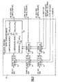
- the in-phase (i_comp) and quadrature-phase (q_comp) component calculation is performed on the resolver sine, cosine and excitation wrap-around sampled A/D data. As each new A/D sample is acquired, the following computation according to the below Equations (1) and (2) is performed on the last 12 received data points.
- Equations (1) and (2) describe the operations performed on a block of samples, in this example 12, that encompass complete cycles of the resolver excitation frequency.
- the Equations (1) and (2) do not illustrate how the computations are indexed and updated upon acquiring each new decimated A/D sample.
- Equations (3) and (4) below are alternative forms of the above equations that illustrate how the samples are updated such that the last 12 filtered and decimated samples are utilized for the in-phase and quadrature phase calculations. Further, to maximize the resolver angle calculation update rate such that a new update is computed at N times the resolver excitation frequency (once per decimated A/D sample), Equations (3) and (4) are utilized.
- Equations (3) and (4) x (n) represents the most recent A/D sample, x (n-1) represents the previous sample, and additional past data samples are further presented according to this convention.
- the disclosed example utilizes the last 12 decimated samples, however, more or less samples could be utilized depending on the desired application and specific system performance required.
- Equations (5) and (6) below are simplified to facilitate implementation by the digital logic of the FPGA 30.
- I n x n ⁇ sin 2 ⁇ ⁇ ⁇ n N + I n ⁇ 1 ⁇ x n ⁇ N ⁇ sin 2 ⁇ ⁇ ⁇ n ⁇ N N q _ comp ,
- Q n x n ⁇ cos 2 ⁇ ⁇ ⁇ n N + Q n ⁇ 1 ⁇ x n ⁇ N ⁇ cos 2 ⁇ ⁇ ⁇ n ⁇ N N
- Equations (5) and (6) provide a simplified alternative to Equations (3) and (4) and require only two multiplies and three summations to produce a single result. Equations (5) and (6) each involve multiplying a properly indexed sine and cosine array by the current A/D sample and adding the result to the previous in-phase and quadrature phase resultant, and then subtracting the oldest sine or cosine term.
- the sine and cosine functions repeat every N samples and can be implemented using a circular look up table including N sample points.
- N is equal to 12.
- An example 12 point circular look up table for sine and cosine inputs is shown below.
- the proper indexing of the sine and cosine array values in the above look-up table provide for computing of the proper four quadrant phase (0-360 degrees) result that is computed based on the final in-phase and quadrature phase results.
- the example look up tables are directed to the disclosed example including 12 samples. The example look up tables could be modified to match the number of desired samples.
- Equations (3), (4), (5), and (6) produce the same resultants and provide a new in-phase and quadrature phase resultant for every new filtered and decimated A/D sample for an update equal to 12 times the resolver frequency in this example.
- the values from the FPGA 30 are input into a processor 38 for transformation into a value, schematically indicated at 46, indicative of an angular position of the rotary device 15 that is communicated to the controller 44.
- the sine, cosine, excitation arid other data generated by the FPGA 30 as indicated above is utilized to provide the desire angular position value 46 that can be utilized by the controller 44.
- the processor 38 performs an initial magnitude calculation on the sine, cosine and excitation values as indicated by the following example equations.
- m scaling factor for converting the results into volts peak referenced to the interface input.
- the values sin_mag_vp and cos_mag_vp are magnitude vectors computed above and as such are always positive resultants. Because the magnitude vector results will always be positive, the arctan function used to compute the resolver angle is forced into the first quadrant. For this reason, as shown below in Equation (10), the i_comp component result of both the sine and cosine resolver inputs are used in conjunction with the arctan function to determine the correct 4-quadrant result.
- angle _ deg ⁇ 360 2 ⁇ ⁇ ⁇ arctan sin _ mag _ vp cos _ mag _ vp ⁇ IF sin _ i _ comp ⁇ 0 ⁇ cos _ i _ comp > 0 360 2 ⁇ ⁇ ⁇ ⁇ 2 + arctan cos _ mag _ vp sin _ mag _ vp ⁇ IF sin _ i _ comp > 0 ⁇ cos _ i _ comp ⁇ 0 360 2 ⁇ ⁇ ⁇ + arctan sin _ mag _ vp cos _ mag _ vp ⁇ IF sin _ i _ comp ⁇ 0 ⁇ cos _ i _ comp ⁇ 0 360 2 ⁇ ⁇ ⁇ 3 ⁇ ⁇ 2 + arctan cos _ mag _ vp sin _ mag _ vp ⁇ IF sin _ i _ comp ⁇ 0 ⁇ ⁇
- the resulting angle_deg value from Equation (10) is the angular value 46 that is input to the controller 44 for use by other systems and processes that require information about the current angular position of the rotary device 15.
- a computing device can be used to implement various functionality, such as that attributable to the method of digital demodulation and other functions performed by the FPGA 30.
- a computing device can include a processor, a memory, and one or more input and/or output (I/O) device interface(s) that are communicatively coupled via a local interface.
- the local interface can include, for example but not limited to, one or more buses and/or other wired or wireless connections.
- the local interface may have additional elements, which are omitted for simplicity, such as controllers, buffers (caches), drivers, repeaters, and receivers to enable communications. Further, the local interface may include address, control, and/or data connections to enable appropriate communications among the aforementioned components.
- the processor may be a hardware device for executing software, particularly software stored in memory.
- the processor can be a custom made or commercially available processor, a central processing unit (CPU), an auxiliary processor among several processors associated with the computing device, a semiconductor based microprocessor (in the form of a microchip or chip set) or generally any device for executing software instructions.
- the memory can include any one or combination of volatile memory elements (e.g., random access memory (RAM, such as DRAM, SRAM, SDRAM, VRAM, etc.)) and/or nonvolatile memory elements (e.g., ROM, hard drive, tape, CD-ROM, etc.).
- volatile memory elements e.g., random access memory (RAM, such as DRAM, SRAM, SDRAM, VRAM, etc.)
- nonvolatile memory elements e.g., ROM, hard drive, tape, CD-ROM, etc.
- the memory may incorporate electronic, magnetic, optical, and/or other types of storage media.
- the memory can also have a distributed architecture, where various components are situated remotely from one another, but can be accessed by the processor.
- the software in the memory may include one or more separate programs, each of which includes an ordered listing of executable instructions for implementing logical functions.
- a system component embodied as software may also be construed as a source program, executable program (object code), script, or any other entity comprising a set of instructions to be performed.
- the program is translated via a compiler, assembler, interpreter, or the like, which may or may not be included within the memory.
- the Input/Output devices that may be coupled to system I/O Interface(s) may include input devices, for example but not limited to, a keyboard, mouse, scanner, microphone, camera, proximity device, etc. Further, the Input/Output devices may also include output devices, for example but not limited to, a printer, display, etc. Finally, the Input/Output devices may further include devices that communicate both as inputs and outputs, for instance but not limited to, a modulator/demodulator (modem; for accessing another device, system, or network), a radio frequency (RF) or other transceiver, a telephonic interface, a bridge, a router, etc.
- modem for accessing another device, system, or network
- RF radio frequency
- the processor can be configured to execute software stored within the memory, to communicate data to and from the memory, and to generally control operations of the computing device pursuant to the software.
- Software in memory, in whole or in part, is read by the processor, perhaps buffered within the processor, and then executed.
- the example resolver interface 10 includes several built in test and self check features to verify the operation of the resolver 16 and the resolver interface. 10.
- An off scale driver signal 40 is provided for both the sine and cosine inputs 12, 14.
- the off scale drive signal inputs a large DC voltage above the normal voltage in response to the lack of the sine/cosine inputs 12, 14.
- the increased DC voltage is detected by the digital demodulator as an increased average value.
- a DC voltage will register as a 0 value in the i_sine and i_cosine values.
- the "0" value is a valid positional indication of the resolver 16 and therefore does not by itself indicate any malfunction. However, an increase in the average value above that which would be expected for any condition of the resolver does provide the desired indication of a malfunction.
- the off scale drive feature provides an indication of a problem condition without any separate control or special test protocol.
- the example resolver interface 10 also includes an internal excitation channel 42 that can be switched over to feed each of the anti-aliasing filters 20, 22, 24 instead of the usual sine, cosine and external excitation signals. Accordingly, the resulting signal received by the FPGA module 30 is known. If the signal received through the multiplexer 26 and A/D converter 28 is not as expected, a fault condition is indicated that would provide an indication that something within the resolver interface 10 is not operating as desired. If the signal received is as expected, then something other than the resolver interface 10 is not operating as is desired. As appreciated, if a fault condition occurs while the external excitation signal is being fed to the resolver 16, then the interface 10 can switch over to the internal channel. If no fault is detected with the internal channel sending an input to each of the filters 20, 22, 24, it is likely that something is not as desired in the resolver 16 or a connection to the resolver.
- the digital demodulation technique presented here computes the sine and cosine signal magnitudes and is not adversely affected by sine or cosine signal phase shifts introduced by the cabling system, the signal conditioning circuitry, or the resolver sensor itself.
- the present digital demodulation is not affected by expected reasonable phase shift error introduced between the resolver's excitation and sine and cosine output signals or any reasonable phase shift introduced between the resolver's sinewave and cosine outputs.
- An additional test and confirmation process is part of the resolver interface 10 to provide an indication of the phase difference between the resolver sine output and the cosine output relative to the resolver excitation.
- a relative phase difference between the excitation, sine and cosine signals from the resolver are commonly part of the resolver specification.
- the relative phase of the excitation, sine and cosine signals can be computed and utilized to determine sensor health. If the expected phase difference between any of the resolver outputs deviates out of an expected range, it may evidence degradation in resolver performance. Such degradation can be utilized to predict potential failures in resolver performance.
Landscapes
- Engineering & Computer Science (AREA)
- Theoretical Computer Science (AREA)
- Power Engineering (AREA)
- Physics & Mathematics (AREA)
- General Physics & Mathematics (AREA)
- Transmission And Conversion Of Sensor Element Output (AREA)
Claims (13)
- Drehmelderschnittstelle (10), Folgendes umfassend:einen Analog-Digital-Wandler (A/D-Wandler, 28), der zum Abtasten bei einer Abtastfrequenz angeordnet ist;einen Multiplexer (26), der zum Zeitmultiplexen des A/D-Wandlers zwischen einem Sinuseingang (12) eines Sinussignalpfads, einem Cosinuseingang (14) eines Cosinussignalpfads und einem Anregungssignal (18) angeordnet ist;eine Anregungsquelle (32) zum Erzeugen des Anregungssignals, das zum Erzeugen des Sinuseingangs und des Cosinuseingangs, die mit dem Anregungssignal synchronisiert sind, und zum Produzieren der Abtastfrequenz für den A/D-Wandler verwendet wird; und wobei die Drehmelderschnittstelle durch Folgendes gekennzeichnet ist:
Einschließen eines internen Kanals (42) zum Leiten des Anregungssignals durch den Sinussignalpfad und den Cosinussignalpfad, um Fehlerzustände zu isolieren. - Drehmelderschnittstelle nach Anspruch 1, einschließlich eines ersten Anti-Aliasing-Filters (20) zum Filtern des Sinuseingangs, eines zweiten Anti-Aliasing-Filters (22) zum Filtern des Cosinuseingangs.
- Drehmelderschnittstelle nach Anspruch 2, wobei der erste Anti-Aliasing-Filter (20) und der zweite Anti-Aliasing-Filter (22) einen dualen OP-Verstärker und ein gemeinsames Verstärkerpaket zum Bereitstellen einer gemeinsamen Zunahme des Sinus- und Cosinuseingangs umfassen.
- Drehmelderschnittstelle nach Anspruch 2 oder 3, wobei der erste Anti-Aliasing-Filter (20) und der zweite Anti-Aliasing-Filter (22) einen Butterworth-Filter vierter Ordnung umfassen.
- Drehmelderschnittstelle nach Anspruch 1, 2, 3 oder 4, einschließlich eines Field Programmable Gate Arrays (FPGA, 30), das dazu programmiert ist, von dem A/D-Wandler (28) einen digitalen Filter für jedes der Sinus-, Cosinus- und Anregungssignale zu implementieren.
- Drehmelderschnittstelle nach Anspruch 5, wobei das FPGA (30) ein digitales Demodulatormodul (36) einschließt, das eine digitale Demodulationsberechnung zum Bestimmen einer Magnitude und einer Vierquadrantenposition des Sinus- und Cosinuseingangs durchführt.
- Verfahren zum Überwachen von Eingangssignalen von einem Drehmelder (16), wobei das Verfahren die folgenden Schritte umfasst:Erzeugen eines Anregungssignals bei einem Field Programmable Gate Array (FPGA, 30);Erzeugen eines Sinuseingangs und eines Cosinuseingangs, die eine Position eines rotierenden Elements anzeigen, mithilfe des Drehmelders (16) basierend auf dem Anregungssignal, und Leiten des Anregungssignals über einen internen Kanal (42) durch den Sinusignalpfad und den Cosinussignalpfad, um Fehlerzustände zu isolieren;Herausfiltern von Bandfrequenzen von dem Sinuseingang und dem Cosinuseingang in separaten Anti-Aliasing-Filtern (20, 22);Zeitmultiplexen des Sinuseingangs und des Cosinuseingangs an einen einzelnen Analog-Digital-Wandler (28);digitales Filtern jedes von dem Sinuseingang und dem Cosinuseingang in dem FPGA; undDemodulieren des Sinuseingangs und des Cosinuseingangs in dem FPGA bei einer Rate, die mit einer Frequenz des Anregungssignals synchronisiert ist,Routen des Anregungssignals durch einen separaten Anti-Aliasing-Filter (24) und Zeitmultiplexen des Anregungssignals zu dem A/D-Wandler (28) mit dem Sinus- und Cosinuseingang zum Prüfen von Sinus- und Cosinussignalbearbeitungspfaden.
- Verfahren nach Anspruch 7, einschließlich des Schritts des Abtastens des Sinus- und Cosinuseingangs mit 120-facher Frequenz des Anregungssignals.
- Verfahren nach Anspruch 8, einschließlich des Schritts des Dezimierens des Sinuseingangs und des Cosinuseingangs von dem A/D-Wandler um einen Faktor 10, um eine dezimierte Abtastfrequenz bereitzustellen, die einem 12-fachen der Anregungsfrequenz entspricht.
- Differentialpositionssensorschnittstelle (10), Folgendes umfassend:einen Analog-Digital-Wandler (A/D-Wandler, 28), der zum Abtasten bei einer Abtastfrequenz angeordnet ist;einen Multiplexer (26), der zum Zeitmultiplexen des A/D-Wandlers zwischen einem Sinuseingang (12) eines Sinussignalpfads, einem Cosinuseingang (14) eines Cosinussignalpfads und einem Anregungssignal angeordnet ist;eine Anregungsquelle (32) zum Erzeugen des Anregungssignals, das zum Erzeugen des Sinuseingangs und des Cosinuseingangs, die mit dem Anregungssignal synchronisiert sind, und zum Produzieren der Abtastfrequenz für den A/D-Wandler verwendet wird; und wobei die Differentialpositionsschnittstelle durch Folgendes gekennzeichnet ist:
Einschließen eines internen Kanals (42) zum Leiten des Anregungssignals durch den Sinussignalpfad und den Cosinussignalpfad, um Fehlerzustände zu isolieren. - Differentialpositionssensorschnittstelle nach Anspruch 10, einschließlich eines ersten Anti-Aliasing-Filters (20) zum Filtern des Sinuseingangs und eines zweiten Anti-Aliasing-Filters (22) zum Filtern des Cosinuseingangs.
- Differentialpositionssensorschnittstelle nach Anspruch 10 oder 11, einschließlich eines Field Programmable Gate Arrays (FPGA) (30), das dazu programmiert ist, von dem A/D-Wandler (28) einen digitalen Filter für jedes des Sinus- und Cosinuseingangs und der Anregungssignale zu implementieren.
- Differentialpositionssensorschnittstelle nach Anspruch 12, wobei das FPGA (30) ein digitales Demodulatormodul (36) einschließt, das eine digitale Demodulationsberechnung zum Bestimmen einer Magnitude und einer Vierquadrantenposition des Sinus- und Cosinuseingangs durchführt.
Applications Claiming Priority (1)
| Application Number | Priority Date | Filing Date | Title |
|---|---|---|---|
| US12/252,603 US7977936B2 (en) | 2008-10-16 | 2008-10-16 | Resolver interface and signal conditioner |
Publications (3)
| Publication Number | Publication Date |
|---|---|
| EP2177879A2 EP2177879A2 (de) | 2010-04-21 |
| EP2177879A3 EP2177879A3 (de) | 2014-03-26 |
| EP2177879B1 true EP2177879B1 (de) | 2020-04-29 |
Family
ID=41606729
Family Applications (1)
| Application Number | Title | Priority Date | Filing Date |
|---|---|---|---|
| EP09251431.4A Active EP2177879B1 (de) | 2008-10-16 | 2009-05-29 | Drehmelderschnittstelle und Signalformer |
Country Status (3)
| Country | Link |
|---|---|
| US (1) | US7977936B2 (de) |
| EP (1) | EP2177879B1 (de) |
| JP (2) | JP4965613B2 (de) |
Cited By (1)
| Publication number | Priority date | Publication date | Assignee | Title |
|---|---|---|---|---|
| DE102011003758B4 (de) | 2011-02-08 | 2022-12-08 | Robert Bosch Gmbh | Verfahren zur Resolverchipdiagnose, Resolverchipdiagnosevorrichtung und Computerprogrammprodukt |
Families Citing this family (28)
| Publication number | Priority date | Publication date | Assignee | Title |
|---|---|---|---|---|
| IT1402545B1 (it) | 2010-10-29 | 2013-09-13 | Cefriel Società Consortile A Responsabilità Limitata | Apparecchi, sistema e procedimento per rilevare incidenti |
| IT1402544B1 (it) | 2010-10-29 | 2013-09-13 | Dainese Spa | Apparecchi, sistema e procedimento per la protezione personale |
| CN102111158B (zh) * | 2010-11-23 | 2013-05-01 | 广州数控设备有限公司 | 对位置传感器的正余弦信号细分和数据编码的装置及实现方法 |
| CN102435133A (zh) * | 2011-09-02 | 2012-05-02 | 北京邮电大学 | 一种基于fpga的旋转变压器测角系统 |
| JP5802588B2 (ja) * | 2012-03-23 | 2015-10-28 | 株式会社東芝 | 角度検出装置およびモータ駆動制御装置 |
| JP5733251B2 (ja) * | 2012-03-27 | 2015-06-10 | 株式会社デンソー | 位置検出装置 |
| JP5733250B2 (ja) | 2012-03-27 | 2015-06-10 | 株式会社デンソー | 位置検出装置 |
| US9068861B2 (en) * | 2012-08-24 | 2015-06-30 | Hamilton Sundstrand Corporation | Resolver interface |
| US9231719B2 (en) | 2013-03-12 | 2016-01-05 | Hamilton Sundstrand Corporation | Method and apparatus for multiplexed time aligned analog input sampling |
| US9059732B2 (en) | 2013-03-21 | 2015-06-16 | Hamilton Sundstrand Corporation | Resolver-to-digital converter |
| US9448275B2 (en) * | 2013-06-25 | 2016-09-20 | The Boeing Company | Fault detection of four wire variable differential transformer sensors |
| CN104949605B (zh) * | 2014-03-31 | 2019-11-15 | 通用电气公司 | 位置检测模块,位置检测系统及方法 |
| JP6527704B2 (ja) | 2015-01-29 | 2019-06-05 | ルネサスエレクトロニクス株式会社 | 半導体装置 |
| CN105865318A (zh) * | 2016-03-30 | 2016-08-17 | 杭州和利时自动化有限公司 | 应用于lvdt位移传感器的非相敏数字解调系统及方法 |
| US11231296B2 (en) | 2016-04-18 | 2022-01-25 | Hamilton Sundstrand Corporation | Systems and methods for determining rotational position |
| CN108225479B (zh) * | 2016-12-12 | 2021-12-24 | 中国航空工业集团公司西安航空计算技术研究所 | 航空油量传感器交流正弦可变激励源发生电路 |
| CN108732527A (zh) * | 2018-08-06 | 2018-11-02 | 国网四川省电力公司电力科学研究院 | 基于广域同步测量的互感器性能在线监测系统 |
| CN109828717B (zh) * | 2019-01-31 | 2022-04-12 | 哈尔滨工业大学 | 多个旋转变压器的并行数据采集电路及自动采集方法 |
| CN110031025B (zh) * | 2019-04-19 | 2024-05-03 | 武汉蔚铭自控科技有限公司 | 一种数字输出的分装式旋转变压器 |
| CN111077822A (zh) * | 2019-12-24 | 2020-04-28 | 中国航天时代电子有限公司 | 一种基于软件波道配置项重构的多信道可编程采集系统 |
| US11144162B1 (en) * | 2020-11-20 | 2021-10-12 | Synaptics Incorporated | Device and method for sensor electrode testing |
| CN112629570B (zh) * | 2020-11-25 | 2022-04-08 | 武汉先同科技有限公司 | 一种基于fpga的编码器滤波算法 |
| US11362508B1 (en) | 2021-04-20 | 2022-06-14 | Hamilton Sundstrand Corporation | Partial RMS based over-current detection for VDT excitation |
| CN113848343B (zh) * | 2021-09-13 | 2024-11-19 | 中国人民解放军92601部队 | 一种火炮角度参数计量检测装置 |
| CN114322733A (zh) * | 2021-12-31 | 2022-04-12 | 辰工(无锡)工业科技有限公司 | 精密测量传感器的激励信号生成方法、系统和存储介质 |
| US12055390B2 (en) * | 2022-03-30 | 2024-08-06 | Hamilton Sundstrand Corporation | Standalone resolver angle verification |
| CN115494758B (zh) * | 2022-08-31 | 2025-10-24 | 株洲变流技术国家工程研究中心有限公司 | 一种旋转变压器的数据采集装置以及解码方法 |
| CN119995411B (zh) * | 2025-04-09 | 2025-07-11 | 峰岹科技(深圳)股份有限公司 | 旋转变压器的解码方法、旋转数字转换器及存储介质 |
Citations (1)
| Publication number | Priority date | Publication date | Assignee | Title |
|---|---|---|---|---|
| EP0215724B1 (de) * | 1985-08-28 | 1991-04-17 | United Technologies Corporation | Apparat und Methode zur Erhaltung der Phaseninformation zur Verwendung mit einem induktiven Mehrspulenverschiebungssensor |
Family Cites Families (29)
| Publication number | Priority date | Publication date | Assignee | Title |
|---|---|---|---|---|
| US3735391A (en) * | 1971-08-05 | 1973-05-22 | United Aircraft Corp | Magnetic synchro angle resolver |
| US4062005A (en) * | 1975-11-04 | 1977-12-06 | Lockheed Electronics Co., Inc. | Synchro-to-digital converter employing common processing apparatus |
| IT1160621B (it) * | 1978-08-31 | 1987-03-11 | Olivetti Controllo Numerico | Apparecchiatura per la misura numerica di posizioni |
| US4328483A (en) * | 1980-02-01 | 1982-05-04 | Sperry Corporation | Multiplexed-demultiplexed synchro demodulation apparatus |
| US4511884A (en) * | 1982-11-09 | 1985-04-16 | C & A Products, Inc. | Programmable limit switch system using a resolver-to-digital angle converter |
| US4472669A (en) * | 1982-12-23 | 1984-09-18 | General Electric Company | Compensated resolver feedback |
| US5189620A (en) * | 1989-10-06 | 1993-02-23 | United Technologies Corporation | Control system for gas turbine helicopter engines and the like |
| US5134397A (en) * | 1991-06-17 | 1992-07-28 | Hughes Aircraft Company | Phase compensation for electromagnetic resolvers |
| NL9101615A (nl) * | 1991-09-24 | 1993-04-16 | Ind Contractors Holland Bv | Positiemeting met radio-frequente transponders. |
| US5235274A (en) * | 1991-10-07 | 1993-08-10 | Honeywell Inc. | Pulsed excitation position sensor system using linear variable differential transducers with multiplexing |
| DE4224225C2 (de) * | 1992-07-22 | 1996-03-14 | Walter Dr Mehnert | Schaltungsanordnung für einen induktiven Stellungsgeber |
| US5488323A (en) * | 1994-12-14 | 1996-01-30 | United Technologies Corporation | True hysteresis window comparator for use in monitoring changes in switch resistance |
| US6211633B1 (en) * | 1996-07-10 | 2001-04-03 | Hamilton Sundstrand Corporation | Synchronous sampling circuit for a sensorless switching reluctance machine system |
| JP3368837B2 (ja) * | 1998-08-05 | 2003-01-20 | トヨタ自動車株式会社 | レゾルバ信号処理装置 |
| DE19841763C1 (de) * | 1998-09-11 | 2000-02-10 | Texas Instruments Deutschland | Verfahren zur digitalen Auswertung der analogen Ausgangssignale eines Resolvers |
| US6331759B1 (en) * | 1999-04-27 | 2001-12-18 | The Boeing Company | Pulse drive angle measurement system and method |
| JP4355395B2 (ja) * | 1999-05-19 | 2009-10-28 | 株式会社アミテック | 位置検出データ生成方法及び装置 |
| KR100390315B1 (ko) * | 2000-12-30 | 2003-07-07 | 삼성탈레스 주식회사 | 절대 회전 각도 측정 장치 및 그 제어 방법 |
| DE60135149D1 (de) * | 2000-12-30 | 2008-09-11 | Hamilton Sundstrand Corp | Schaltsteuersystem und drehzahlregelung für einen bürstenlosen motor |
| US20040001015A1 (en) * | 2000-12-30 | 2004-01-01 | Games John E. | Processing analog signals with respect to timing of related rotary parts |
| US6754610B2 (en) * | 2001-05-16 | 2004-06-22 | Raytheon Company | Digital signal processing of resolver rotor angle signals |
| JP4543133B2 (ja) * | 2001-05-23 | 2010-09-15 | 多摩川精機株式会社 | レゾルバ信号の演算処理装置 |
| US20040027118A1 (en) * | 2002-08-12 | 2004-02-12 | James Lenz | Proximity sensor circuit with programmable logic device controller |
| US20040193988A1 (en) * | 2003-03-26 | 2004-09-30 | James Saloio | Engine speed sensor with fault detection |
| JP2005037305A (ja) * | 2003-07-17 | 2005-02-10 | Sanyo Denki Co Ltd | レゾルバの検出位置補正方法及び装置 |
| JP4521258B2 (ja) * | 2004-01-28 | 2010-08-11 | 日立オートモティブシステムズ株式会社 | レゾルバ/デジタル変換器及びこれを用いた制御システム |
| JP4391288B2 (ja) * | 2004-03-26 | 2009-12-24 | ミネベア株式会社 | 高精度1xvr型レゾルバ |
| JP2006017659A (ja) * | 2004-07-05 | 2006-01-19 | Tamagawa Seiki Co Ltd | アナログ信号のデジタル変換方法 |
| US7432836B2 (en) * | 2006-08-01 | 2008-10-07 | Hamilton Sundstrand Corporation | Multiplexed signal conditioner |
-
2008
- 2008-10-16 US US12/252,603 patent/US7977936B2/en not_active Expired - Fee Related
-
2009
- 2009-05-29 EP EP09251431.4A patent/EP2177879B1/de active Active
- 2009-08-26 JP JP2009195005A patent/JP4965613B2/ja active Active
-
2012
- 2012-01-19 JP JP2012009116A patent/JP2012073276A/ja not_active Withdrawn
Patent Citations (1)
| Publication number | Priority date | Publication date | Assignee | Title |
|---|---|---|---|---|
| EP0215724B1 (de) * | 1985-08-28 | 1991-04-17 | United Technologies Corporation | Apparat und Methode zur Erhaltung der Phaseninformation zur Verwendung mit einem induktiven Mehrspulenverschiebungssensor |
Cited By (1)
| Publication number | Priority date | Publication date | Assignee | Title |
|---|---|---|---|---|
| DE102011003758B4 (de) | 2011-02-08 | 2022-12-08 | Robert Bosch Gmbh | Verfahren zur Resolverchipdiagnose, Resolverchipdiagnosevorrichtung und Computerprogrammprodukt |
Also Published As
| Publication number | Publication date |
|---|---|
| EP2177879A2 (de) | 2010-04-21 |
| JP2012073276A (ja) | 2012-04-12 |
| JP4965613B2 (ja) | 2012-07-04 |
| EP2177879A3 (de) | 2014-03-26 |
| JP2010096750A (ja) | 2010-04-30 |
| US7977936B2 (en) | 2011-07-12 |
| US20100097052A1 (en) | 2010-04-22 |
Similar Documents
| Publication | Publication Date | Title |
|---|---|---|
| EP2177879A2 (de) | Drehmelderschnittstelle und Signalformer | |
| US10634554B2 (en) | Integrated vibration measurement and analysis system | |
| US7509862B2 (en) | System and method for providing vibration detection in turbomachinery | |
| EP1884746B1 (de) | Multiplex-Signalverstärker | |
| CN107709933B (zh) | 用于分析转动角度传感器的信号的装置和方法 | |
| JP5173962B2 (ja) | レゾルバ/デジタル変換装置およびレゾルバ/デジタル変換方法 | |
| US9897469B2 (en) | Resolver phase compensation | |
| US20190086241A1 (en) | Position-measuring device and method for operating a position-measuring device | |
| EP3594630B1 (de) | Kompensation ungeradzahliger harmonischer verzerrung für drehmelder/lvdt | |
| EP3239662A1 (de) | Systeme und verfahren zur bestimmung einer drehposition | |
| DE10036090B4 (de) | Verfahren zur Unterdrückung systematischer Fehler von inkrementellen Lagegebern | |
| EP2955488B1 (de) | Multiplexsignalabtaster und -verbesserer | |
| EP1747641B1 (de) | Sensormessverfahren und system mit universaldatenkonzentratoren | |
| US5606515A (en) | Sensor conditioning circuitry for use with electrically excited transducers | |
| CN104870943A (zh) | 冗余的信号检测 | |
| CN116073728A (zh) | 车辆电机旋变角度的解码方法、系统、设备和存储介质 | |
| KR100758492B1 (ko) | 직교필터를 이용한 주파수 추정 장치 및 그 방법 | |
| JP3602078B2 (ja) | 人工衛星の姿勢検出装置 | |
| US8928312B2 (en) | Method, device and system for monitoring the determination of a rotor angle of a rotating shaft by means of a resolver | |
| JP2008196937A (ja) | 回転角度位置算出装置 | |
| CN117419923A (zh) | 适用于发动机的流水型硬件相位解算方法以及解算系统 | |
| JP2009068887A (ja) | 回転角検出装置 | |
| JP3847656B2 (ja) | 角度検出装置における温度検出方法、角度検出装置及び角度検出装置を備えたアクチュエータ制御システム | |
| CN116054821B (zh) | 用于恢复载波信号的装置及方法 | |
| US20250293701A1 (en) | Digital finite impulse response filtering method and associated filtering device |
Legal Events
| Date | Code | Title | Description |
|---|---|---|---|
| PUAI | Public reference made under article 153(3) epc to a published international application that has entered the european phase |
Free format text: ORIGINAL CODE: 0009012 |
|
| AK | Designated contracting states |
Kind code of ref document: A2 Designated state(s): AT BE BG CH CY CZ DE DK EE ES FI FR GB GR HR HU IE IS IT LI LT LU LV MC MK MT NL NO PL PT RO SE SI SK TR |
|
| AX | Request for extension of the european patent |
Extension state: AL BA RS |
|
| PUAL | Search report despatched |
Free format text: ORIGINAL CODE: 0009013 |
|
| AK | Designated contracting states |
Kind code of ref document: A3 Designated state(s): AT BE BG CH CY CZ DE DK EE ES FI FR GB GR HR HU IE IS IT LI LT LU LV MC MK MT NL NO PL PT RO SE SI SK TR |
|
| AX | Request for extension of the european patent |
Extension state: AL BA RS |
|
| RIC1 | Information provided on ipc code assigned before grant |
Ipc: H03M 1/64 20060101ALI20140217BHEP Ipc: G01D 5/22 20060101AFI20140217BHEP |
|
| 17P | Request for examination filed |
Effective date: 20140925 |
|
| RBV | Designated contracting states (corrected) |
Designated state(s): AT BE BG CH CY CZ DE DK EE ES FI FR GB GR HR HU IE IS IT LI LT LU LV MC MK MT NL NO PL PT RO SE SI SK TR |
|
| STAA | Information on the status of an ep patent application or granted ep patent |
Free format text: STATUS: EXAMINATION IS IN PROGRESS |
|
| 17Q | First examination report despatched |
Effective date: 20170519 |
|
| GRAP | Despatch of communication of intention to grant a patent |
Free format text: ORIGINAL CODE: EPIDOSNIGR1 |
|
| STAA | Information on the status of an ep patent application or granted ep patent |
Free format text: STATUS: GRANT OF PATENT IS INTENDED |
|
| RIC1 | Information provided on ipc code assigned before grant |
Ipc: H03M 1/64 20060101ALI20191106BHEP Ipc: H03M 1/12 20060101ALI20191106BHEP Ipc: G01D 5/22 20060101AFI20191106BHEP |
|
| INTG | Intention to grant announced |
Effective date: 20191210 |
|
| RAP1 | Party data changed (applicant data changed or rights of an application transferred) |
Owner name: HAMILTON SUNDSTRAND CORPORATION |
|
| GRAS | Grant fee paid |
Free format text: ORIGINAL CODE: EPIDOSNIGR3 |
|
| GRAA | (expected) grant |
Free format text: ORIGINAL CODE: 0009210 |
|
| STAA | Information on the status of an ep patent application or granted ep patent |
Free format text: STATUS: THE PATENT HAS BEEN GRANTED |
|
| AK | Designated contracting states |
Kind code of ref document: B1 Designated state(s): AT BE BG CH CY CZ DE DK EE ES FI FR GB GR HR HU IE IS IT LI LT LU LV MC MK MT NL NO PL PT RO SE SI SK TR |
|
| REG | Reference to a national code |
Ref country code: GB Ref legal event code: FG4D |
|
| REG | Reference to a national code |
Ref country code: CH Ref legal event code: EP |
|
| REG | Reference to a national code |
Ref country code: AT Ref legal event code: REF Ref document number: 1263992 Country of ref document: AT Kind code of ref document: T Effective date: 20200515 |
|
| REG | Reference to a national code |
Ref country code: DE Ref legal event code: R096 Ref document number: 602009061870 Country of ref document: DE |
|
| REG | Reference to a national code |
Ref country code: IE Ref legal event code: FG4D |
|
| REG | Reference to a national code |
Ref country code: NL Ref legal event code: MP Effective date: 20200429 |
|
| REG | Reference to a national code |
Ref country code: LT Ref legal event code: MG4D |
|
| PG25 | Lapsed in a contracting state [announced via postgrant information from national office to epo] |
Ref country code: LT Free format text: LAPSE BECAUSE OF FAILURE TO SUBMIT A TRANSLATION OF THE DESCRIPTION OR TO PAY THE FEE WITHIN THE PRESCRIBED TIME-LIMIT Effective date: 20200429 Ref country code: PT Free format text: LAPSE BECAUSE OF FAILURE TO SUBMIT A TRANSLATION OF THE DESCRIPTION OR TO PAY THE FEE WITHIN THE PRESCRIBED TIME-LIMIT Effective date: 20200831 Ref country code: GR Free format text: LAPSE BECAUSE OF FAILURE TO SUBMIT A TRANSLATION OF THE DESCRIPTION OR TO PAY THE FEE WITHIN THE PRESCRIBED TIME-LIMIT Effective date: 20200730 Ref country code: SE Free format text: LAPSE BECAUSE OF FAILURE TO SUBMIT A TRANSLATION OF THE DESCRIPTION OR TO PAY THE FEE WITHIN THE PRESCRIBED TIME-LIMIT Effective date: 20200429 Ref country code: NO Free format text: LAPSE BECAUSE OF FAILURE TO SUBMIT A TRANSLATION OF THE DESCRIPTION OR TO PAY THE FEE WITHIN THE PRESCRIBED TIME-LIMIT Effective date: 20200729 Ref country code: FI Free format text: LAPSE BECAUSE OF FAILURE TO SUBMIT A TRANSLATION OF THE DESCRIPTION OR TO PAY THE FEE WITHIN THE PRESCRIBED TIME-LIMIT Effective date: 20200429 Ref country code: IS Free format text: LAPSE BECAUSE OF FAILURE TO SUBMIT A TRANSLATION OF THE DESCRIPTION OR TO PAY THE FEE WITHIN THE PRESCRIBED TIME-LIMIT Effective date: 20200829 |
|
| REG | Reference to a national code |
Ref country code: AT Ref legal event code: MK05 Ref document number: 1263992 Country of ref document: AT Kind code of ref document: T Effective date: 20200429 |
|
| PG25 | Lapsed in a contracting state [announced via postgrant information from national office to epo] |
Ref country code: HR Free format text: LAPSE BECAUSE OF FAILURE TO SUBMIT A TRANSLATION OF THE DESCRIPTION OR TO PAY THE FEE WITHIN THE PRESCRIBED TIME-LIMIT Effective date: 20200429 Ref country code: BG Free format text: LAPSE BECAUSE OF FAILURE TO SUBMIT A TRANSLATION OF THE DESCRIPTION OR TO PAY THE FEE WITHIN THE PRESCRIBED TIME-LIMIT Effective date: 20200729 Ref country code: LV Free format text: LAPSE BECAUSE OF FAILURE TO SUBMIT A TRANSLATION OF THE DESCRIPTION OR TO PAY THE FEE WITHIN THE PRESCRIBED TIME-LIMIT Effective date: 20200429 |
|
| PG25 | Lapsed in a contracting state [announced via postgrant information from national office to epo] |
Ref country code: NL Free format text: LAPSE BECAUSE OF FAILURE TO SUBMIT A TRANSLATION OF THE DESCRIPTION OR TO PAY THE FEE WITHIN THE PRESCRIBED TIME-LIMIT Effective date: 20200429 |
|
| PG25 | Lapsed in a contracting state [announced via postgrant information from national office to epo] |
Ref country code: LI Free format text: LAPSE BECAUSE OF NON-PAYMENT OF DUE FEES Effective date: 20200531 Ref country code: MC Free format text: LAPSE BECAUSE OF FAILURE TO SUBMIT A TRANSLATION OF THE DESCRIPTION OR TO PAY THE FEE WITHIN THE PRESCRIBED TIME-LIMIT Effective date: 20200429 Ref country code: RO Free format text: LAPSE BECAUSE OF FAILURE TO SUBMIT A TRANSLATION OF THE DESCRIPTION OR TO PAY THE FEE WITHIN THE PRESCRIBED TIME-LIMIT Effective date: 20200429 Ref country code: CZ Free format text: LAPSE BECAUSE OF FAILURE TO SUBMIT A TRANSLATION OF THE DESCRIPTION OR TO PAY THE FEE WITHIN THE PRESCRIBED TIME-LIMIT Effective date: 20200429 Ref country code: ES Free format text: LAPSE BECAUSE OF FAILURE TO SUBMIT A TRANSLATION OF THE DESCRIPTION OR TO PAY THE FEE WITHIN THE PRESCRIBED TIME-LIMIT Effective date: 20200429 Ref country code: EE Free format text: LAPSE BECAUSE OF FAILURE TO SUBMIT A TRANSLATION OF THE DESCRIPTION OR TO PAY THE FEE WITHIN THE PRESCRIBED TIME-LIMIT Effective date: 20200429 Ref country code: AT Free format text: LAPSE BECAUSE OF FAILURE TO SUBMIT A TRANSLATION OF THE DESCRIPTION OR TO PAY THE FEE WITHIN THE PRESCRIBED TIME-LIMIT Effective date: 20200429 Ref country code: CH Free format text: LAPSE BECAUSE OF NON-PAYMENT OF DUE FEES Effective date: 20200531 Ref country code: IT Free format text: LAPSE BECAUSE OF FAILURE TO SUBMIT A TRANSLATION OF THE DESCRIPTION OR TO PAY THE FEE WITHIN THE PRESCRIBED TIME-LIMIT Effective date: 20200429 Ref country code: DK Free format text: LAPSE BECAUSE OF FAILURE TO SUBMIT A TRANSLATION OF THE DESCRIPTION OR TO PAY THE FEE WITHIN THE PRESCRIBED TIME-LIMIT Effective date: 20200429 |
|
| REG | Reference to a national code |
Ref country code: DE Ref legal event code: R097 Ref document number: 602009061870 Country of ref document: DE |
|
| PG25 | Lapsed in a contracting state [announced via postgrant information from national office to epo] |
Ref country code: SK Free format text: LAPSE BECAUSE OF FAILURE TO SUBMIT A TRANSLATION OF THE DESCRIPTION OR TO PAY THE FEE WITHIN THE PRESCRIBED TIME-LIMIT Effective date: 20200429 Ref country code: PL Free format text: LAPSE BECAUSE OF FAILURE TO SUBMIT A TRANSLATION OF THE DESCRIPTION OR TO PAY THE FEE WITHIN THE PRESCRIBED TIME-LIMIT Effective date: 20200429 |
|
| PLBE | No opposition filed within time limit |
Free format text: ORIGINAL CODE: 0009261 |
|
| STAA | Information on the status of an ep patent application or granted ep patent |
Free format text: STATUS: NO OPPOSITION FILED WITHIN TIME LIMIT |
|
| REG | Reference to a national code |
Ref country code: BE Ref legal event code: MM Effective date: 20200531 |
|
| PG25 | Lapsed in a contracting state [announced via postgrant information from national office to epo] |
Ref country code: LU Free format text: LAPSE BECAUSE OF NON-PAYMENT OF DUE FEES Effective date: 20200529 |
|
| 26N | No opposition filed |
Effective date: 20210201 |
|
| PG25 | Lapsed in a contracting state [announced via postgrant information from national office to epo] |
Ref country code: IE Free format text: LAPSE BECAUSE OF NON-PAYMENT OF DUE FEES Effective date: 20200529 |
|
| PG25 | Lapsed in a contracting state [announced via postgrant information from national office to epo] |
Ref country code: BE Free format text: LAPSE BECAUSE OF NON-PAYMENT OF DUE FEES Effective date: 20200531 Ref country code: SI Free format text: LAPSE BECAUSE OF FAILURE TO SUBMIT A TRANSLATION OF THE DESCRIPTION OR TO PAY THE FEE WITHIN THE PRESCRIBED TIME-LIMIT Effective date: 20200429 |
|
| PG25 | Lapsed in a contracting state [announced via postgrant information from national office to epo] |
Ref country code: TR Free format text: LAPSE BECAUSE OF FAILURE TO SUBMIT A TRANSLATION OF THE DESCRIPTION OR TO PAY THE FEE WITHIN THE PRESCRIBED TIME-LIMIT Effective date: 20200429 Ref country code: MT Free format text: LAPSE BECAUSE OF FAILURE TO SUBMIT A TRANSLATION OF THE DESCRIPTION OR TO PAY THE FEE WITHIN THE PRESCRIBED TIME-LIMIT Effective date: 20200429 Ref country code: CY Free format text: LAPSE BECAUSE OF FAILURE TO SUBMIT A TRANSLATION OF THE DESCRIPTION OR TO PAY THE FEE WITHIN THE PRESCRIBED TIME-LIMIT Effective date: 20200429 |
|
| PG25 | Lapsed in a contracting state [announced via postgrant information from national office to epo] |
Ref country code: MK Free format text: LAPSE BECAUSE OF FAILURE TO SUBMIT A TRANSLATION OF THE DESCRIPTION OR TO PAY THE FEE WITHIN THE PRESCRIBED TIME-LIMIT Effective date: 20200429 |
|
| PGFP | Annual fee paid to national office [announced via postgrant information from national office to epo] |
Ref country code: GB Payment date: 20220426 Year of fee payment: 14 Ref country code: FR Payment date: 20220421 Year of fee payment: 14 Ref country code: DE Payment date: 20220420 Year of fee payment: 14 |
|
| REG | Reference to a national code |
Ref country code: DE Ref legal event code: R119 Ref document number: 602009061870 Country of ref document: DE |
|
| GBPC | Gb: european patent ceased through non-payment of renewal fee |
Effective date: 20230529 |
|
| PG25 | Lapsed in a contracting state [announced via postgrant information from national office to epo] |
Ref country code: DE Free format text: LAPSE BECAUSE OF NON-PAYMENT OF DUE FEES Effective date: 20231201 Ref country code: GB Free format text: LAPSE BECAUSE OF NON-PAYMENT OF DUE FEES Effective date: 20230529 |
|
| PG25 | Lapsed in a contracting state [announced via postgrant information from national office to epo] |
Ref country code: FR Free format text: LAPSE BECAUSE OF NON-PAYMENT OF DUE FEES Effective date: 20230531 |