EP2168177B1 - Méthode de fabrication d'un module de piles solaires en couches minces - Google Patents
Méthode de fabrication d'un module de piles solaires en couches minces Download PDFInfo
- Publication number
- EP2168177B1 EP2168177B1 EP08785978.1A EP08785978A EP2168177B1 EP 2168177 B1 EP2168177 B1 EP 2168177B1 EP 08785978 A EP08785978 A EP 08785978A EP 2168177 B1 EP2168177 B1 EP 2168177B1
- Authority
- EP
- European Patent Office
- Prior art keywords
- electrode
- line
- layers
- solar cell
- photoactive layer
- Prior art date
- Legal status (The legal status is an assumption and is not a legal conclusion. Google has not performed a legal analysis and makes no representation as to the accuracy of the status listed.)
- Active
Links
- 238000000034 method Methods 0.000 title claims description 107
- 239000010409 thin film Substances 0.000 title claims description 59
- 238000004519 manufacturing process Methods 0.000 title claims description 45
- 230000008569 process Effects 0.000 claims description 55
- 239000000758 substrate Substances 0.000 claims description 49
- 239000000463 material Substances 0.000 claims description 29
- 238000005240 physical vapour deposition Methods 0.000 claims description 21
- 230000005855 radiation Effects 0.000 claims description 19
- 239000004065 semiconductor Substances 0.000 claims description 13
- 238000000623 plasma-assisted chemical vapour deposition Methods 0.000 claims description 12
- 150000001875 compounds Chemical class 0.000 claims description 9
- 229910021417 amorphous silicon Inorganic materials 0.000 claims description 8
- 238000007641 inkjet printing Methods 0.000 claims description 8
- 229910052751 metal Inorganic materials 0.000 claims description 7
- 239000002184 metal Substances 0.000 claims description 7
- 230000000704 physical effect Effects 0.000 claims description 7
- 238000005530 etching Methods 0.000 claims description 5
- 229910004613 CdTe Inorganic materials 0.000 claims description 4
- 239000000155 melt Substances 0.000 claims description 3
- 229910021424 microcrystalline silicon Inorganic materials 0.000 claims description 3
- 229910000577 Silicon-germanium Inorganic materials 0.000 claims description 2
- 238000004544 sputter deposition Methods 0.000 claims description 2
- 239000000853 adhesive Substances 0.000 claims 2
- 230000001070 adhesive effect Effects 0.000 claims 2
- 239000010410 layer Substances 0.000 description 144
- 238000000576 coating method Methods 0.000 description 44
- 239000011248 coating agent Substances 0.000 description 42
- 238000005229 chemical vapour deposition Methods 0.000 description 22
- 239000002390 adhesive tape Substances 0.000 description 16
- 239000011521 glass Substances 0.000 description 14
- 238000000926 separation method Methods 0.000 description 11
- 238000000059 patterning Methods 0.000 description 8
- 230000015572 biosynthetic process Effects 0.000 description 7
- 229910052710 silicon Inorganic materials 0.000 description 7
- 238000004140 cleaning Methods 0.000 description 5
- 238000000151 deposition Methods 0.000 description 5
- 239000012535 impurity Substances 0.000 description 5
- XUIMIQQOPSSXEZ-UHFFFAOYSA-N Silicon Chemical compound [Si] XUIMIQQOPSSXEZ-UHFFFAOYSA-N 0.000 description 4
- 230000008021 deposition Effects 0.000 description 4
- 238000004518 low pressure chemical vapour deposition Methods 0.000 description 4
- 239000010703 silicon Substances 0.000 description 4
- VYPSYNLAJGMNEJ-UHFFFAOYSA-N Silicium dioxide Chemical compound O=[Si]=O VYPSYNLAJGMNEJ-UHFFFAOYSA-N 0.000 description 3
- 230000008901 benefit Effects 0.000 description 3
- 239000004020 conductor Substances 0.000 description 3
- 239000005357 flat glass Substances 0.000 description 3
- 229910052738 indium Inorganic materials 0.000 description 3
- 229920000642 polymer Polymers 0.000 description 3
- 238000004886 process control Methods 0.000 description 3
- 238000012545 processing Methods 0.000 description 3
- 238000001953 recrystallisation Methods 0.000 description 3
- 229910021332 silicide Inorganic materials 0.000 description 3
- FVBUAEGBCNSCDD-UHFFFAOYSA-N silicide(4-) Chemical compound [Si-4] FVBUAEGBCNSCDD-UHFFFAOYSA-N 0.000 description 3
- 229910052814 silicon oxide Inorganic materials 0.000 description 3
- 229910045601 alloy Inorganic materials 0.000 description 2
- 239000000956 alloy Substances 0.000 description 2
- 229910052793 cadmium Inorganic materials 0.000 description 2
- 230000008859 change Effects 0.000 description 2
- 239000002019 doping agent Substances 0.000 description 2
- 229910052733 gallium Inorganic materials 0.000 description 2
- 239000011810 insulating material Substances 0.000 description 2
- 239000012212 insulator Substances 0.000 description 2
- 230000001678 irradiating effect Effects 0.000 description 2
- 150000002739 metals Chemical class 0.000 description 2
- 230000009467 reduction Effects 0.000 description 2
- 230000011218 segmentation Effects 0.000 description 2
- 229910052709 silver Inorganic materials 0.000 description 2
- XOLBLPGZBRYERU-UHFFFAOYSA-N tin dioxide Chemical compound O=[Sn]=O XOLBLPGZBRYERU-UHFFFAOYSA-N 0.000 description 2
- 238000001771 vacuum deposition Methods 0.000 description 2
- 229910004298 SiO 2 Inorganic materials 0.000 description 1
- 239000006096 absorbing agent Substances 0.000 description 1
- 238000000862 absorption spectrum Methods 0.000 description 1
- 229910052782 aluminium Inorganic materials 0.000 description 1
- 239000012080 ambient air Substances 0.000 description 1
- QVGXLLKOCUKJST-UHFFFAOYSA-N atomic oxygen Chemical compound [O] QVGXLLKOCUKJST-UHFFFAOYSA-N 0.000 description 1
- 230000005540 biological transmission Effects 0.000 description 1
- 229920001940 conductive polymer Polymers 0.000 description 1
- 239000013078 crystal Substances 0.000 description 1
- 230000001419 dependent effect Effects 0.000 description 1
- 238000005137 deposition process Methods 0.000 description 1
- 238000013461 design Methods 0.000 description 1
- 238000001514 detection method Methods 0.000 description 1
- 238000011161 development Methods 0.000 description 1
- 230000018109 developmental process Effects 0.000 description 1
- 238000009792 diffusion process Methods 0.000 description 1
- 239000000428 dust Substances 0.000 description 1
- 239000012777 electrically insulating material Substances 0.000 description 1
- 238000005566 electron beam evaporation Methods 0.000 description 1
- 238000005538 encapsulation Methods 0.000 description 1
- 238000005516 engineering process Methods 0.000 description 1
- 230000005496 eutectics Effects 0.000 description 1
- 239000011888 foil Substances 0.000 description 1
- 238000010438 heat treatment Methods 0.000 description 1
- APFVFJFRJDLVQX-UHFFFAOYSA-N indium atom Chemical compound [In] APFVFJFRJDLVQX-UHFFFAOYSA-N 0.000 description 1
- 239000011261 inert gas Substances 0.000 description 1
- 238000009413 insulation Methods 0.000 description 1
- 239000011229 interlayer Substances 0.000 description 1
- 239000004922 lacquer Substances 0.000 description 1
- 230000000873 masking effect Effects 0.000 description 1
- 230000007246 mechanism Effects 0.000 description 1
- 238000010327 methods by industry Methods 0.000 description 1
- 238000002156 mixing Methods 0.000 description 1
- 239000000203 mixture Substances 0.000 description 1
- 229910052750 molybdenum Inorganic materials 0.000 description 1
- 230000003287 optical effect Effects 0.000 description 1
- 239000001301 oxygen Substances 0.000 description 1
- 229910052760 oxygen Inorganic materials 0.000 description 1
- 239000003973 paint Substances 0.000 description 1
- 239000002245 particle Substances 0.000 description 1
- 230000002093 peripheral effect Effects 0.000 description 1
- 238000002294 plasma sputter deposition Methods 0.000 description 1
- 238000011417 postcuring Methods 0.000 description 1
- 230000001681 protective effect Effects 0.000 description 1
- 238000007788 roughening Methods 0.000 description 1
- 238000007789 sealing Methods 0.000 description 1
- LIVNPJMFVYWSIS-UHFFFAOYSA-N silicon monoxide Chemical compound [Si-]#[O+] LIVNPJMFVYWSIS-UHFFFAOYSA-N 0.000 description 1
- 239000002195 soluble material Substances 0.000 description 1
- 239000002904 solvent Substances 0.000 description 1
- 238000001228 spectrum Methods 0.000 description 1
- 238000005507 spraying Methods 0.000 description 1
- 230000005654 stationary process Effects 0.000 description 1
- 238000003860 storage Methods 0.000 description 1
- 229920001187 thermosetting polymer Polymers 0.000 description 1
Images


Classifications
-
- H—ELECTRICITY
- H01—ELECTRIC ELEMENTS
- H01L—SEMICONDUCTOR DEVICES NOT COVERED BY CLASS H10
- H01L31/00—Semiconductor devices sensitive to infrared radiation, light, electromagnetic radiation of shorter wavelength or corpuscular radiation and specially adapted either for the conversion of the energy of such radiation into electrical energy or for the control of electrical energy by such radiation; Processes or apparatus specially adapted for the manufacture or treatment thereof or of parts thereof; Details thereof
- H01L31/04—Semiconductor devices sensitive to infrared radiation, light, electromagnetic radiation of shorter wavelength or corpuscular radiation and specially adapted either for the conversion of the energy of such radiation into electrical energy or for the control of electrical energy by such radiation; Processes or apparatus specially adapted for the manufacture or treatment thereof or of parts thereof; Details thereof adapted as photovoltaic [PV] conversion devices
- H01L31/042—PV modules or arrays of single PV cells
-
- H—ELECTRICITY
- H01—ELECTRIC ELEMENTS
- H01L—SEMICONDUCTOR DEVICES NOT COVERED BY CLASS H10
- H01L31/00—Semiconductor devices sensitive to infrared radiation, light, electromagnetic radiation of shorter wavelength or corpuscular radiation and specially adapted either for the conversion of the energy of such radiation into electrical energy or for the control of electrical energy by such radiation; Processes or apparatus specially adapted for the manufacture or treatment thereof or of parts thereof; Details thereof
- H01L31/0248—Semiconductor devices sensitive to infrared radiation, light, electromagnetic radiation of shorter wavelength or corpuscular radiation and specially adapted either for the conversion of the energy of such radiation into electrical energy or for the control of electrical energy by such radiation; Processes or apparatus specially adapted for the manufacture or treatment thereof or of parts thereof; Details thereof characterised by their semiconductor bodies
- H01L31/036—Semiconductor devices sensitive to infrared radiation, light, electromagnetic radiation of shorter wavelength or corpuscular radiation and specially adapted either for the conversion of the energy of such radiation into electrical energy or for the control of electrical energy by such radiation; Processes or apparatus specially adapted for the manufacture or treatment thereof or of parts thereof; Details thereof characterised by their semiconductor bodies characterised by their crystalline structure or particular orientation of the crystalline planes
- H01L31/0392—Semiconductor devices sensitive to infrared radiation, light, electromagnetic radiation of shorter wavelength or corpuscular radiation and specially adapted either for the conversion of the energy of such radiation into electrical energy or for the control of electrical energy by such radiation; Processes or apparatus specially adapted for the manufacture or treatment thereof or of parts thereof; Details thereof characterised by their semiconductor bodies characterised by their crystalline structure or particular orientation of the crystalline planes including thin films deposited on metallic or insulating substrates ; characterised by specific substrate materials or substrate features or by the presence of intermediate layers, e.g. barrier layers, on the substrate
- H01L31/03923—Semiconductor devices sensitive to infrared radiation, light, electromagnetic radiation of shorter wavelength or corpuscular radiation and specially adapted either for the conversion of the energy of such radiation into electrical energy or for the control of electrical energy by such radiation; Processes or apparatus specially adapted for the manufacture or treatment thereof or of parts thereof; Details thereof characterised by their semiconductor bodies characterised by their crystalline structure or particular orientation of the crystalline planes including thin films deposited on metallic or insulating substrates ; characterised by specific substrate materials or substrate features or by the presence of intermediate layers, e.g. barrier layers, on the substrate including AIBIIICVI compound materials, e.g. CIS, CIGS
-
- H—ELECTRICITY
- H01—ELECTRIC ELEMENTS
- H01L—SEMICONDUCTOR DEVICES NOT COVERED BY CLASS H10
- H01L31/00—Semiconductor devices sensitive to infrared radiation, light, electromagnetic radiation of shorter wavelength or corpuscular radiation and specially adapted either for the conversion of the energy of such radiation into electrical energy or for the control of electrical energy by such radiation; Processes or apparatus specially adapted for the manufacture or treatment thereof or of parts thereof; Details thereof
- H01L31/0248—Semiconductor devices sensitive to infrared radiation, light, electromagnetic radiation of shorter wavelength or corpuscular radiation and specially adapted either for the conversion of the energy of such radiation into electrical energy or for the control of electrical energy by such radiation; Processes or apparatus specially adapted for the manufacture or treatment thereof or of parts thereof; Details thereof characterised by their semiconductor bodies
- H01L31/036—Semiconductor devices sensitive to infrared radiation, light, electromagnetic radiation of shorter wavelength or corpuscular radiation and specially adapted either for the conversion of the energy of such radiation into electrical energy or for the control of electrical energy by such radiation; Processes or apparatus specially adapted for the manufacture or treatment thereof or of parts thereof; Details thereof characterised by their semiconductor bodies characterised by their crystalline structure or particular orientation of the crystalline planes
- H01L31/0392—Semiconductor devices sensitive to infrared radiation, light, electromagnetic radiation of shorter wavelength or corpuscular radiation and specially adapted either for the conversion of the energy of such radiation into electrical energy or for the control of electrical energy by such radiation; Processes or apparatus specially adapted for the manufacture or treatment thereof or of parts thereof; Details thereof characterised by their semiconductor bodies characterised by their crystalline structure or particular orientation of the crystalline planes including thin films deposited on metallic or insulating substrates ; characterised by specific substrate materials or substrate features or by the presence of intermediate layers, e.g. barrier layers, on the substrate
- H01L31/03925—Semiconductor devices sensitive to infrared radiation, light, electromagnetic radiation of shorter wavelength or corpuscular radiation and specially adapted either for the conversion of the energy of such radiation into electrical energy or for the control of electrical energy by such radiation; Processes or apparatus specially adapted for the manufacture or treatment thereof or of parts thereof; Details thereof characterised by their semiconductor bodies characterised by their crystalline structure or particular orientation of the crystalline planes including thin films deposited on metallic or insulating substrates ; characterised by specific substrate materials or substrate features or by the presence of intermediate layers, e.g. barrier layers, on the substrate including AIIBVI compound materials, e.g. CdTe, CdS
-
- H—ELECTRICITY
- H01—ELECTRIC ELEMENTS
- H01L—SEMICONDUCTOR DEVICES NOT COVERED BY CLASS H10
- H01L31/00—Semiconductor devices sensitive to infrared radiation, light, electromagnetic radiation of shorter wavelength or corpuscular radiation and specially adapted either for the conversion of the energy of such radiation into electrical energy or for the control of electrical energy by such radiation; Processes or apparatus specially adapted for the manufacture or treatment thereof or of parts thereof; Details thereof
- H01L31/04—Semiconductor devices sensitive to infrared radiation, light, electromagnetic radiation of shorter wavelength or corpuscular radiation and specially adapted either for the conversion of the energy of such radiation into electrical energy or for the control of electrical energy by such radiation; Processes or apparatus specially adapted for the manufacture or treatment thereof or of parts thereof; Details thereof adapted as photovoltaic [PV] conversion devices
- H01L31/042—PV modules or arrays of single PV cells
- H01L31/0445—PV modules or arrays of single PV cells including thin film solar cells, e.g. single thin film a-Si, CIS or CdTe solar cells
- H01L31/046—PV modules composed of a plurality of thin film solar cells deposited on the same substrate
- H01L31/0465—PV modules composed of a plurality of thin film solar cells deposited on the same substrate comprising particular structures for the electrical interconnection of adjacent PV cells in the module
-
- Y—GENERAL TAGGING OF NEW TECHNOLOGICAL DEVELOPMENTS; GENERAL TAGGING OF CROSS-SECTIONAL TECHNOLOGIES SPANNING OVER SEVERAL SECTIONS OF THE IPC; TECHNICAL SUBJECTS COVERED BY FORMER USPC CROSS-REFERENCE ART COLLECTIONS [XRACs] AND DIGESTS
- Y02—TECHNOLOGIES OR APPLICATIONS FOR MITIGATION OR ADAPTATION AGAINST CLIMATE CHANGE
- Y02E—REDUCTION OF GREENHOUSE GAS [GHG] EMISSIONS, RELATED TO ENERGY GENERATION, TRANSMISSION OR DISTRIBUTION
- Y02E10/00—Energy generation through renewable energy sources
- Y02E10/50—Photovoltaic [PV] energy
- Y02E10/541—CuInSe2 material PV cells
-
- Y—GENERAL TAGGING OF NEW TECHNOLOGICAL DEVELOPMENTS; GENERAL TAGGING OF CROSS-SECTIONAL TECHNOLOGIES SPANNING OVER SEVERAL SECTIONS OF THE IPC; TECHNICAL SUBJECTS COVERED BY FORMER USPC CROSS-REFERENCE ART COLLECTIONS [XRACs] AND DIGESTS
- Y02—TECHNOLOGIES OR APPLICATIONS FOR MITIGATION OR ADAPTATION AGAINST CLIMATE CHANGE
- Y02E—REDUCTION OF GREENHOUSE GAS [GHG] EMISSIONS, RELATED TO ENERGY GENERATION, TRANSMISSION OR DISTRIBUTION
- Y02E10/00—Energy generation through renewable energy sources
- Y02E10/50—Photovoltaic [PV] energy
- Y02E10/543—Solar cells from Group II-VI materials
-
- Y—GENERAL TAGGING OF NEW TECHNOLOGICAL DEVELOPMENTS; GENERAL TAGGING OF CROSS-SECTIONAL TECHNOLOGIES SPANNING OVER SEVERAL SECTIONS OF THE IPC; TECHNICAL SUBJECTS COVERED BY FORMER USPC CROSS-REFERENCE ART COLLECTIONS [XRACs] AND DIGESTS
- Y02—TECHNOLOGIES OR APPLICATIONS FOR MITIGATION OR ADAPTATION AGAINST CLIMATE CHANGE
- Y02E—REDUCTION OF GREENHOUSE GAS [GHG] EMISSIONS, RELATED TO ENERGY GENERATION, TRANSMISSION OR DISTRIBUTION
- Y02E10/00—Energy generation through renewable energy sources
- Y02E10/50—Photovoltaic [PV] energy
- Y02E10/548—Amorphous silicon PV cells
-
- Y—GENERAL TAGGING OF NEW TECHNOLOGICAL DEVELOPMENTS; GENERAL TAGGING OF CROSS-SECTIONAL TECHNOLOGIES SPANNING OVER SEVERAL SECTIONS OF THE IPC; TECHNICAL SUBJECTS COVERED BY FORMER USPC CROSS-REFERENCE ART COLLECTIONS [XRACs] AND DIGESTS
- Y02—TECHNOLOGIES OR APPLICATIONS FOR MITIGATION OR ADAPTATION AGAINST CLIMATE CHANGE
- Y02P—CLIMATE CHANGE MITIGATION TECHNOLOGIES IN THE PRODUCTION OR PROCESSING OF GOODS
- Y02P70/00—Climate change mitigation technologies in the production process for final industrial or consumer products
- Y02P70/50—Manufacturing or production processes characterised by the final manufactured product
Definitions
- the invention relates to a method for producing a thin-film solar cell module with a plurality of arranged on a common substrate and electrically connected in series segments.
- Thin-film solar cell modules also called thin-film photovoltaic modules, have photoactive layers with layer thicknesses in the order of micrometers.
- the semiconductor material used in the photoactive layer or layers may be amorphous or microcrystalline. A combination of layers of amorphous and layers of microcrystalline semiconductor material within a cell is also possible, for example in the so-called tandem cells and the so-called triple cells.
- the semiconductor materials used are Si, Ge and compound semiconductors such as CdTe or Cu (In, Ga) Se2 (abbreviated to CIS or CIGS).
- thin-film solar cell modules are usually divided into a plurality of segments.
- the strip-shaped and usually a few millimeters to centimeters wide segments usually run parallel to an edge of the module.
- the segments are formed by individual layers of the layer structure of the solar cell are interrupted by thin dividing lines in continuous substrate.
- the separating lines lead to the fact that identical layers of adjacent segments are electrically insulated from one another and, on the other hand, that subsequently applied layers can be electrically connected along a contact line to underlying layers. With a suitable arrangement of the separating lines can be achieved in this way a series connection of the individual segments.
- the formation of a parting line takes place immediately after the application of a layer. Since the deposition of layers is usually done under vacuum conditions, but the separation lines are spatially separated therefrom under atmospheric conditions, the prior art fabrication process requires complicated process control. Furthermore, there is the risk of the storage of impurities between the layers of a solar cell in the frequent infeed and discharge operations in and out of the vacuum. Also, during the patterning operations, removed material deposited on the layers may constitute such an impurity.
- the EP 0 320 089 A2 relates to a solar cell comprising a semiconductor layer and a conductive layer formed on a flexible substrate, divided into individual segments interconnected by interconnection layers in series.
- the US 2006/278497 A1 relates to a manufacturing plant with two vacuum locks and a plurality of process chambers between the vacuum locks.
- the object is achieved by a method for producing a thin-film solar cell module having a plurality of segments arranged on a common substrate and electrically connected in series, the method comprising the steps of applying layers to the substrate to form at least one Electrode and a photoactive layer sequence and a further electrode and has steps for patterning applied layers to form the plurality of segments.
- the steps of patterning include forming a separation line which interrupts the electrode, the photoactive layer sequence, and the further electrode, and depositing an electrically conductive adhesive tape or conductive paste of conductive paste across the parting line, thereby interrupting the further electrode Trennline electrically closed again.
- At least one electrode and a photoactive layer sequence and another electrode are applied before performing steps for patterning.
- a set of at least three layer deposition processes is first performed before structuring steps are performed for segmentation.
- the summary grouping of process steps, each performed under comparable conditions (eg, vacuum versus atmospheric conditions), facilitates process control and is useful in reducing inter-layer impurities in thin film solar cell modules.
- structuring of already applied layers takes place by creating a separation line by irradiation of laser radiation and / or by mechanical scribing and / or by selective etching.
- laser radiation is particularly preferably irradiated in such a way that one or more layers are removed locally or that one or more layers are locally heated in such a way that the physical properties of at least one of the layers, in particular their conductivity, changes.
- structuring of already applied layers takes place by creating a contact line by irradiating laser radiation.
- laser light is particularly preferably irradiated in such a way that superimposed layers of different materials are locally heated and a material compound is formed which has physical properties deviating from the original materials and, in particular, is conductive.
- an insulating line of an electrically insulating material created within one of the dividing lines is an insulating line of an electrically insulating material created within one of the dividing lines.
- the insulating line is applied by an inkjet printing process.
- a structuring of subsequent layers to be applied by means of a cover made of a soluble material is applied by means of a cover made of a soluble material.
- the cover line is applied by an inkjet printing process.
- the aforementioned advantageous embodiment of the method according to the first aspect of the invention specify structuring measures which are suitable for structuring a (single) layer also within a layer stack having at least two layers applied to one another. They therefore represent ideal structuring measures for the method according to the application.
- a thin film solar cell module having a plurality of segments electrically connected in series comprises an electrically conductive adhesive tape or a strand of conductive paste in the region of a parting line which interrupts a first electrode of the thin film solar cell module to form the segments and a second electrode.
- the electrically conductive adhesive tape or the conductive paste strand is applied to the second electrode to restore the electrical connection.
- the various layers are, for example, structured such that series connection can be carried out after at least three layers have already been applied.
- the summary of the process steps for the application of the layers results in the thin-film solar cell modules in smaller impurities, for example, by frequent in- and Ausschleusevone, and thus in a better layer quality, resulting in a higher efficiency of the cell.
- the process steps for patterning of layers can be summarized, resulting in a better positioning of structuring measures in different layers to each other. This results in a small contact area for the series connection and consequently a higher area yield of the cell.
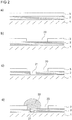
- FIG. 1 shows the layer structure of a thin-film solar cell module according to the prior art in a schematic representation.
- a first electrode 2 On a substrate 1, a first electrode 2, a photoactive layer sequence 3 and a second electrode 4 is applied.
- the first electrode 2, the photoactive layer sequence 3 and the second electrode 4 are laterally interrupted by parting lines 10, 11, 12.
- the three separating lines 10, 11, 12 are in turn laterally spaced from each other and divide the illustrated section of the thin-film solar cell module into a first segment 5 to the left of the dividing line 10, a second segment 7 to the right of the dividing line 12 and an intermediate contacting region 6.
- the electrodes 2, 4 and the photoactive layer sequence 3 are applied to thin-film solar cell modules in vacuum processes.
- PVD processes physical vapor deposition
- plasma sputtering or electron beam evaporation or CVD processes chemical vapor deposition
- CVD processes chemical vapor deposition
- LPCVD low pressure CVD
- PECVD plasma enhanced CVD
- group IV amorphous or microcrystalline semiconductors for example a-Si, a-SiGe, ⁇ C-Si, or compound semiconductors such as, for example, CdTe or Cu (In, Ga) Se2 (CIS for short or CIGS called) are used.
- layers of different materials mentioned can be combined in the photoactive layer sequence 3.
- partially reflective layers (intermediate reflectors) made of a conductive oxide and / or a conductive semiconductor layer may be provided in the photoactive layer sequence 3.
- the photoactive layer sequence 3 typically comprises at least one p- and one n-doped semiconductor layer, that is to say a diode junction.
- the p- and n-doped layers are usually separated by an extended intrinsic layer (i-layer).
- i-layer extended intrinsic layer
- a plurality of pin layer stacks with different absorption spectra can be provided one above the other.
- the Si tandem cell has, for example, a pin layer stack of a-Si and a pin layer stack of ⁇ C-Si, and in the case of the Si triple cell a pin layer stack of a-Si (Ge) is additionally provided.
- the photoactive layer sequence 3 is not limited to a pin or nip layer stack (diode junction) but comprises multiple stacks such as those of tandem or triple cells.
- the p-doped layer faces the sun.
- the production process a distinction is made between so-called pin cells and nip cells based on the sequence in which the differently doped layers of the photoactive layer sequence 3 are applied.
- the (growth) substrate 1 is transparent and, in the case of the finished module, also forms the carrier substrate facing the sun.
- (flat) glass is used.
- glass or even a (metal) foil can be used as a growth substrate.
- the carrier substrate, through which the sunlight is incident during operation, is only laminated to the module at the end of the production process.
- the nip layer stack remains connected to the growth substrate.
- pin cells show pin cells. This is purely illustrative and not limiting. All methods described in the application are applicable to both pin cells and nip cells.
- the solar facing first electrode 2 which is also referred to as the front side electrode, usually made of transparent conductive oxides (TCO, transparent conductive oxides), such as SnO2 or ZnO or ITO (indium tinn oxide), educated.
- TCO transparent conductive oxides
- the second electrode 4 facing away from the sun also referred to below as the backside electrode, may likewise have a TCO layer or else be formed by metals such as Ag, Al, Mo or a combination of TCO and a metal layer.
- the first electrode 2 applied first may comprise a metal layer in the case of a nip cell and represents the rear side electrode remote from the sun during operation. Accordingly, the last applied second electrode 4 is made transparent and forms the front side electrode facing the sun.
- the front side electrode 2, for example, TCO, on the substrate 1, for example, glass first applied.
- the dividing line 10 is generated in the front side electrode 2 by laser radiation of suitable wavelength of 1064 nm, for example, or by mechanical scribing or by selective etching. This parting line 10 extends over the entire width of the module (in the figure perpendicular to the page level).
- the laser radiation can be irradiated both through the substrate 1 and from the layer side.
- the dividing line 10 divides the electrode 2 in its entire height to a width of 5 to 1000 microns, with typical widths in the range of 10 to 50 microns.
- the photoactive layer sequence 3 is applied and subsequently structured by producing the parting line 11.
- the separation line 11 in the photoactive layer sequence 3 is usually generated by using laser light of a wavelength of 532 nm when using Si as a photoactive material.
- the rear side electrode 4 is applied, which comes in direct contact with the front side electrode 2 in the region of the parting line 11.
- the parting line 12 is created to electrically separate the backside electrode 4 of the first segment 5 from the backside electrode 4 of the second segment 7.
- the substrate 1 laser radiation a wavelength that is not absorbed by the front side electrode 2, but by the photoactive layer sequence 3, for example, again 532 nm, so that the photoactive layer sequence 3 evaporates, wherein the metallic back side electrode 4 can melt and is blasted off in the region of the dividing line 12 or in turn can evaporate.
- the alternating steps for applying the layers and for structuring the layers lead to a series connection of the two segments 5 and 7, as can be seen by the arrows symbolizing the current profile in FIG.
- the contact region 6 in the case of thin-film solar cells, it is desirable to design the contact region 6 as narrow as possible since it represents an inactive surface which reduces the surface yield of the solar cell module.
- the separate patterning processes, between which the substrate is moved to the other process chambers for applying the layers inevitably leads to inaccuracies in the positioning of the parting lines 10, 11, 12 to each other.
- FIG. 2 illustrates a first example of a method of manufacturing a thin film solar cell module.
- first a first electrode 2 and a photoactive layer sequence 3 are applied to a substrate 1.
- the substrate 1 is flat glass
- the first electrode 2 is a front-side electrode made of TCO
- the photoactive layer sequence 3 is a sequence of p-doped, intrinsic and n-doped amorphous or microcrystalline silicon.
- the front-side electrode 2 and the photoactive layer sequence 3 can be applied in successive vacuum coating processes, without the substrate 1 having to be removed from the vacuum for this purpose. It is also possible to start with a substrate 1 which is already provided with a TCO layer as the front-side electrode 2. In that case, only the photoactive layer sequence 3 is to be applied.
- a first structuring step takes place, in which the photoactive layer sequence 3 is interrupted to form a separation line 20 over a width of> 100 ⁇ m and typically 150 ⁇ m. This can be done, for example, by introducing laser radiation having a wavelength of 532 nm either from the layer side or through the substrate 1.
- the resulting layer structure is schematically shown in FIG FIG. 2b shown.
- a further dividing line 21 is produced, which is the front-side electrode 2 on a width of typically 10 to 40 microns interrupts (see Figure 2c ).
- laser radiation of a wavelength of 1046 nm or 355 nm is suitable.
- the dividing line 21 is not positioned centered to the dividing line 20, but is arranged in the left region of the dividing line 20, for example such that the left edges of the dividing lines 20 and 21 are spaced approximately 20 to 30 ⁇ m laterally from one another.
- the dividing line 21 can also be generated by means of laser radiation which is irradiated from the layer side or from the substrate side.
- the laser radiation required for forming the parting lines 20 and 21 is provided by a single process head which moves over the substrate 1, so that a positioning of the two parting lines 20 and 21 relative to one another is as exact as possible over the entire length of the parting lines is guaranteed.
- an insulating line 22 equal to an electrically insulating strand along the parting line 21 applied.
- the insulating line 22 fills the dividing line 21 and projects about 20 to 30 ⁇ m into the dividing line 20 on both sides, so that the left edge of the dividing line 20 is isolated and passivated. It is important, however, that a sufficient, typically 20 to 50 microns wide area of the front side electrode 2 in the dividing line 20 is not covered by the insulating line 22.
- the height of the insulating line 22 may typically be 5 to 50 ⁇ m.
- an ink-jet printing method is particularly suitable.
- an insulator material can an electrically insulating and post-curing polymer can be used.
- the height to width ratio of the insulating line 22 can be determined both by the application technique of the insulator material and its flow properties.
- a surface should preferably be formed which is free from edges and sections running perpendicular to the substrate, so that it can subsequently be overgrown well by the back contact 4 to be applied subsequently.
- Figure 2d is an example of a rather high, round profile and dashed as an alternative a flat profile of the insulating line 22 shown.
- a covering line 23 of soluble lacquer is likewise applied in a strand-like manner over the entire width of the substrate 1 ( FIG. 2e ). Again, this is in turn an ink jet printing method.
- the cover line 23 is a possible box-shaped profile advantageous, as in the FIG. 2e shown in idealized form.
- the width of the cover line 23 is typically 50 ⁇ m, and the distance of the line from the right edge of the parting line 20 should be about 20 to 50 ⁇ m.
- the height of the cover line 23 is not critical, but it should be above the thickness of the still to be applied backside electrode 4.
- both the insulating line 22 and the cover line 23 are advantageous to apply with one and the same process head from the layer side. It is also conceivable that all structuring measures, that is to say the irradiation of laser light to form the separating lines 20 and 21 and the application of the insulating line 22 and the covering line 23, take place from a single process head which works from the layer side. To this Way, the relative positioning of all structuring elements to each other is best ensured. If the insulating line 22 and the cover line 23 are applied by a separate process head after the laser structuring, this second process head can be preceded by an optical detection system, which tracks the position of the process head at the detected position of the separation lines 20 or 21.
- the backside electrode 4 for example a ZnO layer, followed by an Ag and / or Al layer in a vacuum deposition process or possibly in a spray coating process is then carried out.
- the different profiles of the insulating line 22 on the one hand and the cover line 23 on the other hand cause the insulating line 22 is overgrown by a continuous layer, whereas where the flanks of the cover 23 are not or only partially overgrown by the back side electrode 4.
- the soluble paint of the cover line 23 is removed by a suitable solvent, whereby the separation line 24 remains in the backside electrode 4.
- the application of the cover line 23 thus represents a structuring process for a layer still to be applied (here the backside electrode).
- the thin-film solar cell module is characterized by the insulating line 22 overgrown by the rear-side electrode 4 and thus completely enclosed.
- the typical sizes and spacings of the structuring elements given in the preceding description can lead to a width of the contact area of less than 200 ⁇ m, which results in effective utilization of the surface of the thin-film solar cell module.
- FIG. 2h an alternative embodiment of the thin-film solar cell module is shown.
- the dividing line 20 was not over the entire in connection with the FIG. 2b specified width. Rather, a narrower dividing line 25 into which the dividing line 21 is centered this time is introduced and a further dividing line 26 is formed.
- This division into two separating lines interrupting the photoactive layer sequence 3 may be advantageous in terms of process engineering since an overall smaller width has to be removed and correspondingly a smaller laser power is required.
- An advantage of in the FIG. 2 represented method is that two layers or layer sequences (cf. FIG. 2a ) are applied before a first patterning step is performed.
- the number of transfers between different process stations and the number of input and output operations in the necessary vacuum for coating application is kept low.
- all structuring steps can be performed grouped one behind the other in a process station, whereby a respective reorientation of the substrate 1 is omitted before each structuring step. If necessary, it is even possible to perform all structuring steps virtually simultaneously with a process head.
- several of these process heads can be used parallel to each other for processing the contact areas between different segments. In this case, these process heads can be equipped with separate lasers, or supplied by separate lasers, or be supplied by a laser, whose light is supplied to the various process heads via beam splitters.
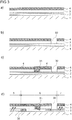
- FIG. 3 shows in an analogous way as FIG. 2 another example.
- the related to FIG. 2 Information about possible materials can be transferred to this example.
- FIG. 3a shows, the front-side electrode 2, the photoactive layer sequence 3 and the back-side electrode 4 are applied to the substrate 1 before a first structuring step is subsequently carried out.
- a separation line 30 in the photoactive layer 3 and the rear side electrode 4 introduced.
- the separation line 30 can be made by irradiation of laser light of a suitable wavelength, for example 532 nm, from the substrate side.
- the in the Figure 3c shown contact line 31 generated.
- laser light of a suitable wavelength from a range of, for example, 200 nm to 10 ⁇ m from the layer side, the back surface electrodes 4 and the photoactive layer 3 melted locally limited, but not evaporated. It is also possible to irradiate the laser light from the substrate side. In this case, for example, wavelengths of about 300 nm to 2 ⁇ are suitable.
- Diffusion processes in the melt form either a silicide, for example AgAlSi with a quasi-metallic conductivity or a eutectic of Si and Ag, which also has a high conductivity.
- a silicide for example AgAlSi with a quasi-metallic conductivity or a eutectic of Si and Ag, which also has a high conductivity.
- current can flow from the back surface electrode 4 into the front side electrode 2 at this point.
- the contact line 31 there is an ohmic contact with the front-side electrode 2.
- the method for forming the contact line 31 is not limited to the material system assumed in the exemplary embodiment.
- the mixture of elements of the photoactive layer 3 and the backside electrode 4 in the locally formed melt can also be used in other systems for forming a conductive material compound or alloy.
- laser radiation of a wavelength absorbed in the front-side electrode for example 1064 nm, is introduced through the substrate 1.
- the power of the laser radiation and the processing time are chosen so that the front side electrode 2 is locally heated and excited to recrystallization processes, without material being physically removed.
- material is therefore not removed at the dividing line, but only in its properties, in particular its conductivity, changed. There is no gap.
- the layers lying above the front-side electrode 2, the photoactive layer 3 and the back-side electrode 4, are not or only insignificantly influenced.
- pulsed laser radiation by locally a short-term heating of the front side electrode 2 can be achieved before the amount of heat dissipated dissipated into the environment. In this way, a high temperature level can be achieved locally for a short time without the environment being significantly heated.
- Pulse durations that are shorter than microseconds and are preferably in the range of nano- or picoseconds are particularly suitable.
- the resulting change in the microstructure of the TCO material of the front side electrode 2 in the region of the dividing line 32 leads to a significant reduction in their conductivity in this area. The reason is that for the conductivity of TCO layers essentially dopants are responsible, which are no longer incorporated in the crystal as a result of the recrystallization process.
- a possible second mechanism that leads to a reduction of the conductivity is one by mixing the material of the front side electrode 2 with the material of the overlying photoactive layer sequence 3.
- the oxygen of the TCO material of the front side electrode 2 forms with the silicon of the photoactive layer sequence 3 electrically insulating silicon oxide (SiO or SiO 2).
- This process is decisively influenced by the high oxide formation enthalpy of silicon.
- front side electrode 2 is electrically interrupted or at least sufficiently lowered its conductivity.
- this method for forming the parting line 32 is not limited to the material system adopted in the embodiment.
- Cd oxides can be formed in the parting line 32, which electrically interrupt the front-side electrode 2 or their conductivity in the region of the parting line Lower 32 sufficiently.
- the result is in the 3d figure represented, in turn, the formed regions of a first segment 5, a second segment 7 and the intervening contact region 6 are shown and in which the current flow in the series connection of the segments 5, 7 is symbolized by arrows.
- the resulting thin-film solar cell module is characterized by the silicon-containing contacting line 31 in the rear-side electrode 4 and by the recrystallized or silicon oxide-containing separating line 32 in the front-side electrode 1.
- all structuring steps can be grouped.
- at least two of the structuring measures namely, the layer-side creation of the parting line 30 and the contacting line 31 are performed from a single process head.
- the remaining structuring measure, the creation of the dividing line 32, can be carried out in the same position of the thin-film solar cell module by a second process head guided parallel to the first process head from the substrate side. It is particularly advantageous that all layers are applied before the group of structuring measures is carried out. To increase the throughput in the structuring also several process heads can also be used in parallel.
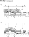
- FIG. 4 shows two embodiments of a method according to the invention for the production of thin-film solar cell modules.
- a front-side contact 2 a photoactive layer sequence 3 and a rear-side contact 4 are applied to a substrate 1. ( FIG. 4a ).
- a dividing line 40 in the back side electrode 4 and the photoactive layer sequence 3 introduced ( FIG. 4b ).
- a contacting line 41 is then formed between the rear-side electrode 4 and the photoactive layer sequence 3.
- a dividing line 42 generates, which interrupts the entire layer structure with the exception of the substrate, so front side electrode 2, photoactive layer sequence 3 and rear side electrode 4.
- the dividing line 42 may preferably be effected by irradiation of laser light of a suitable wavelength (1064 nm or 355 nm) through the substrate.
- a suitable wavelength (1064 nm or 355 nm)
- the photoactive layer sequence 3 and the backside electrode 4 could be removed and in a second step - as in the formation of the parting line 10 (see FIG. 1 ) or the dividing line 20 (see FIG. 2 ) - the front side electrode 2 are removed.
- an electrically conductive adhesive tape 43 is applied over the parting line 42, whereby the unwanted interruption of the backside electrode 4 is electrically reclosed by the parting line 42.
- the electrically conductive adhesive tape 43 may be made of a conductive material, for example Polymer exist.
- the distance of the parting lines 40 and 42 is about 100 ⁇ m. Laying the adhesive tape 43 with such a positional accuracy is technically feasible. In this case, it is not necessary for the conductive adhesive tape 43 to be applied continuously over the entire width of the thin-film solar cell module. It is sufficient if width-distributed portions of the conductive adhesive tape 43 are present as current bridges.
- FIG. 4f An alternative method for connecting the rear side electrode 4 separated by the dividing line 42 is in FIG. 4f shown.
- a conductive strand 44 of a conductive paste is applied, which is chosen in its consistency so that it does not or only insignificantly penetrates into the dividing line 42.
- the application of the conductive paste which may be a thermosetting conductive polymer, may be by ink jet printing.
- the conductive strand 44 is not required to be continuous across the width of the module, although in a more consistent embodiment, a better electrical connection and a better electrical connection are provided protective sealing of the parting line 42 as advantages.
- the thin-film solar cell modules resulting from these two alternative methods are distinguished by the silicide-containing contact line 41 and the adhesive tape 43 or the conductive strand 44 applied to the rear-side electrode 4.
- FIG. 5 shows a production line as a suitable device for carrying out the application-specific manufacturing process for thin-film solar cell modules.
- the production line has a first transport system 50 for receiving a glass substrate 51.
- the transport system 50 opens into a cleaning station 52, which is connected via a first vacuum lock 53 with a coating device 54.
- Coater 54 includes a second transport system 55, a first PVD / (LP) CVD coating station 56, a plurality of PECVD coating stations 57, and a second PVD / (LP) CVD coating station 58.
- the second PVD / (LP) CVD coating station 58 is followed by a second vacuum lock 59 from which a third transport system 60 leads out.
- This third transport system 60 passes through a structuring device 61 which has a plurality of movable process heads 62. After passing through the structuring device 61 on the third transport system 60, a finished thin-film solar cell raw module 63 leaves the production line.
- the starting point for the production of a thin-film solar cell module in the production line shown is the glass substrate 51 supplied via the first transport system 50.
- the production line is designed so that flat glass panes of the usual width of 3.21 m can be picked up and processed.
- the production line can preferably also be coupled directly to a flat glass production line. After cleaning in the cleaning station 52, the glass substrate 51 is fed directly to the first vacuum lock 53 without contact with the surrounding atmosphere. A cleanroom environment for protection against dust particles can therefore be dispensed with.
- the electrode can be applied.
- a low pressure method LPCVD - low pressure CVD
- a (dry) etching device may be integrated in the first PVD / (LP) CVD coating station 56.
- the first PVD / (LP) CVD coating station 56 operates in an in-line process.
- a photoactive layer sequence can be applied in the different PECVD coating stations 57.
- these PECVD coating stations 57 are designed as stationary coating stations.
- the electrode can also be applied in one of these stations in a stationary process.
- the first PVD / (LP) CVD coating station 56 could be dispensed with.
- the glass substrate 51 already has a front electrode, for example by on-line coating in the production line of the glass manufacturer. Also in this case, the first PVD / (LP) CVD coating station 56 could be dispensed with.
- the front side electrodes in a PVD coating process imitation (dry) etching process is used for the necessary roughening of the front electrode.
- the corresponding process station is either integrated into the PVD / (LP) CVD coating station 56 or is one of the PECVD coating stations 57. Due to the arrangement of the coating stations 56, 57 and 58 can be the second transport system 55 in the vacuum of the coating device 54, an unrestricted linear Serve roller drive.
- amorphous p-, i- and n-doped a-Si: H layers and / or microcrystalline p-, i- and n-doped Si layers and, for example, of the PECVD coating stations 57 / or further absorber layers based on a-Si (Ge): H are applied successively.
- the production line is further designed so that the glass substrate 51 after the PECVD coating stations 57 without vacuum interruption passes through the PVD / (LP) CVD coating station 58, wherein the metal layer of a backside electrode is applied, for example, in a sputtering process.
- the PVD / (LP) CVD coating station 58 is again preferably designed as an in-line station for a continuous coating process and may operate in the case of CVD coating in the low pressure process. It is also conceivable that a plurality of PVD / (LP) CVD coating stations 58 are provided in order to be able to deposit various metals, for example Ag and / or Al and / or Mo.
- the glass substrate 51 is again passed out of the vacuum through the second vacuum lock 59 and passes through the structuring device 61 of the production line on the third transport system 60.
- the specified production line can also be used for the production of thin-film solar cell modules based on compound semiconductors (CdTe, CIS).
- the in connection with the FIGS. 2 to 4 described method are characterized by the fact that a grouping in process steps for layer deposition and process steps for structuring, ie the formation of separation, insulating, covering and contact lines, is possible. This is reflected in the summary of the process stations required to deposit the layers in the coating device 54 and the summary of the structuring tools needed for structuring in the structuring device 61.
- the structuring tools used may be lasers, laser transmission optics, inkjet printheads, and adhesive tape applicators. It is advantageous to integrate as many of the structuring tools that are required for interrelated process steps on a process head 62. This applies, for example, lasers of different wavelengths, which produce different, but as correct as possible to be positioned to each other dividing lines.
- a plurality of identical process heads 62 can be present with which different regions of a glass substrate 51 can be processed in parallel.
- the PVD / (LP) CVD coating station 58 may be made separate. Unaffected is the summary of the PECVD coating stations 57 and the PVD / (LP) CVD coating station 56 in the coater 54.
- the finished thin-film solar cell raw module 63 is present. Subsequently, only peripheral processing steps such as encapsulation, stripping of the edges, contacting, etc., are required for the final completion of the thin film solar cell module. These can be carried out independently outside the production line or can also be integrated into the production line.
- the masking line 23 is applied by patterning subsequently applied layers by an ink jet printing method.
- the thin film solar cell module having the plurality of electrically series connected segments 5, 7 is, in one embodiment, by a method as in connection with FIGS Figures 2 . 3 or 5 explained.
- insulating material 22 of insulating material is applied to the region of dividing line 20, 21 interrupting first electrode 2 of the thin-film solar cell module to form segments 5, 7, and is separated from second electrode 4 covered.
- Insulation line 22 in one embodiment includes an insulating polymer.
- the electrode 2 made of an electrically conductive oxide is electrically interrupted by a dividing line 32, wherein the electrode 2 has locally different physical properties in the region of the dividing line 32 than outside the dividing line 32.
- the locally different physical properties in the region of the dividing line 32 in one embodiment are based on a change in the doping after a recrystallization of the electrode 4 in the region of the dividing line 32.
- the locally different physical properties in the region of the dividing line 32 in one embodiment are based on formation of an oxide of an element from the photoactive layer sequence 3 adjacent to the electrode 2 in the region of the dividing line 32.
- the photoactive layer sequence 3 comprises Si, and the dividing line 32 contains Si oxide.
- the thin-film solar cell module having the plurality of electrically connected segments 5, 7 in one embodiment comprises the first electrode 2, the photoactive layer sequence 3 and the second electrode 4.
- the contact line 31 is present, over which the second Electrode 4 with the first electrode 2 for series connection of the segments 5, 7 electrically connected wherein the contact line 31 in the region of the photoactive layer sequence 3 contains a conductive material compound and / or a conductive alloy of elements of the photoactive layer sequence 3 and the second electrode 4.
- the photoactive layer sequence 3 comprises Si and the contact line 31 contains a silicide.
- the electrically conductive adhesive tape 43 or conductive paste strand 44 is in the region of the parting line 42 forming the first electrode 2 of the thin film solar cell module the segments 5, 7 and the second electrode 4 interrupts, applied to restore the electrical connection to the second electrode 4.
- the production line for the production of the thin-film solar cell module on the glass substrate 51 according to one of the in connection with the Figures 2 . 3 4 and 4, respectively, in one embodiment comprises the coating device 54, which has the first vacuum lock 53, the at least two coating stations 56, 57, 58 and the second vacuum lock 59 and is arranged such that the glass substrate 51, after being introduced into the coating device 54 by the first vacuum lock 53 which can pass through at least two coating stations 56, 57, 58 or 503, 56 successively under vacuum conditions, before the substrate is again discharged from the coating device 54 through the second vacuum lock 59.
- the coating device 54 includes the PECVD coating stations 57 and / or the PVD / (LP) CVD coating stations 56, 58.
- the cleaning station 52 is coupled directly to the first vacuum lock 53.
- the first linear roller drive is provided as a transport system 55 by the coating device 54 in one embodiment.
- the structuring device 61 is provided, in which at least two different structuring tools for structuring at least one layer of the thin-film solar cell module are provided on the movable process head 62.
- the process head 62 is configured to simultaneously provide laser radiation in at least two different wavelengths.
- the process head 62 is configured to provide laser radiation and includes the inkjet printing device.
- the process head 62 is configured to lay the adhesive tape 43 on the thin film solar cell module.
Claims (14)
- Procédé servant à fabriquer un module de cellules solaires à couches minces avec une pluralité de segments (5, 7) branchés en série électriquement et disposés sur un substrat (1) commun, comprenant- des étapes pour appliquer des couches sur le substrat (1) pour former au moins une électrode (2), une succession photoactive de couches (3) et une autre électrode (4), et- des étapes pour structurer des couches appliquées pour former la pluralité de segments (5, 7),dans lequel l'électrode (2), la succession photoactive de couches (3) et l'autre électrode (4) sont appliquées avant que des étapes de structuration ne soient exécutées par la suite, dans lequel les étapes de structuration comprennent :- la génération d'une ligne de séparation (42), qui interrompt l'électrode (2), la succession photoactive de couches (3) et l'autre électrode (4),- l'introduction d'une autre ligne de séparation (40) dans l'autre électrode (4) et la succession photoactive de couches (3),- la formation d'une ligne de mise en contact (41) à distance latéralement de l'autre ligne de séparation (40) et entre la ligne de séparation (42) et l'autre ligne de séparation (40), dans lequel l'électrode (2) est reliée électriquement à l'autre électrode (4) pour brancher en série les segments (5, 7) au moyen de la ligne de mise en contact (41),- l'application d'une bande adhésive (43) électriquement conductrice ou d'un brin (44) à partir d'une pâte conductrice sur la ligne de séparation (42), ce qui a pour effet que l'interruption de l'autre électrode (4) par la ligne de séparation (42) est à nouveau fermée électriquement.
- Procédé selon la revendication 1, dans lequel la fabrication d'une électrode (2, 4) comprend l'application d'au moins une couche à partir d'un oxyde conducteur transparent et/ou d'une couche métallique.
- Procédé selon l'une quelconque des revendications 1 ou 2, dans lequel la fabrication de la succession photoactive de couches (3) comprend l'application d'au moins une couche individuelle à partir de Si amorphe ou microcristallin et/ou de SiGe amorphe ou microcristallin et/ou d'un semiconducteur composé, en particulier de CdTe ou de CIS ou de CIGS.
- Procédé selon la revendication 3, dans lequel la fabrication de la succession photoactive de couches (3) comprend l'application d'une couche à dopage p, d'une couche intrinsèque et d'une couche à dopage n composée de Si amorphe et/ou d'une couche à dopage p, d'une couche intrinsèque et d'une couche à dopage n composée de Si microcristallin et/ou d'une couche à dopage p, d'une couche intrinsèque et d'une couche à dopage n composée de Si(Ge) amorphe.
- Procédé selon l'une quelconque des revendications 1 à 4, dans lequel l'application des couches est effectuée par un processus PVD , en particulier un processus de pulvérisation, et/ou un processus CVD, en particulier un processus PECVD.
- Procédé selon l'une quelconque des revendications 1 à 5, dans lequel la ligne de séparation (42) est créée par irradiation d'un rayonnement laser et/ou par gravure mécanique et/ou par décapage sélectif.
- Procédé selon la revendication 6, dans lequel de la lumière laser est émise de telle manière qu'une ou plusieurs couches sont localement enlevées.
- Procédé selon la revendication 6, dans lequel de la lumière laser est émise de telle manière qu'une ou plusieurs couches sont localement réchauffées de telle manière que les propriétés physiques d'au moins une des couches, en particulier leur conductivité, se modifient.
- Procédé selon l'une quelconque des revendications 1 à 8, dans lequel la ligne de contact (41) est créée par irradiation d'un rayonnement laser.
- Procédé selon la revendication 9, dans lequel de la lumière laser est émise de telle manière que des couches superposées à partir de matériaux différents sont réchauffées localement et qu'un composé de matériau se forme, qui a des propriétés physiques divergeant des matériaux d'origine et est en particulier conductive.
- Procédé selon la revendication 10, dans lequel localement une matière fondue des matériaux différents est formée et dans lequel la liaison des matières résulte de la matière fondue.
- Procédé selon l'une quelconque des revendications 6 ou 8, dans lequel une ligne d'isolation est créée à partir d'un matériau électriquement isolant à l'intérieur des lignes de séparation (42).
- Procédé selon la revendication 12, dans lequel la ligne d'isolation est appliquée par un procédé d'impression à jet d'encre.
- Procédé selon l'une quelconque des revendications 1 à 13, comprenant :- la réalisation d'une ligne de contact (41) entre l'autre électrode (4) et l'électrode (2), qui forme un contact ohmique entre l'autre électrode (4) et l'électrode (2), dans lequel la ligne de contact (41) est réalisée avant que la bande adhésive (43) électriquement conductrice ou le brin (44) conducteur composé de la pâte conductrice ne soit appliquée ou appliqué.
Applications Claiming Priority (2)
| Application Number | Priority Date | Filing Date | Title |
|---|---|---|---|
| DE102007032283A DE102007032283A1 (de) | 2007-07-11 | 2007-07-11 | Dünnschichtsolarzellen-Modul und Verfahren zu dessen Herstellung |
| PCT/EP2008/058864 WO2009007375A2 (fr) | 2007-07-11 | 2008-07-08 | Module de piles solaires à couche mince et son procédé de fabrication |
Publications (2)
| Publication Number | Publication Date |
|---|---|
| EP2168177A2 EP2168177A2 (fr) | 2010-03-31 |
| EP2168177B1 true EP2168177B1 (fr) | 2019-09-04 |
Family
ID=40121414
Family Applications (1)
| Application Number | Title | Priority Date | Filing Date |
|---|---|---|---|
| EP08785978.1A Active EP2168177B1 (fr) | 2007-07-11 | 2008-07-08 | Méthode de fabrication d'un module de piles solaires en couches minces |
Country Status (7)
| Country | Link |
|---|---|
| US (2) | US8470615B2 (fr) |
| EP (1) | EP2168177B1 (fr) |
| JP (2) | JP5681845B2 (fr) |
| KR (1) | KR20100032928A (fr) |
| CN (2) | CN101743643B (fr) |
| DE (1) | DE102007032283A1 (fr) |
| WO (1) | WO2009007375A2 (fr) |
Families Citing this family (28)
| Publication number | Priority date | Publication date | Assignee | Title |
|---|---|---|---|---|
| WO2011027532A1 (fr) * | 2009-09-04 | 2011-03-10 | 株式会社アルバック | Procédé et appareil de fabrication de module de cellule solaire |
| GB2474665B (en) * | 2009-10-22 | 2011-10-12 | M Solv Ltd | Method and apparatus for dividing thin film device into separate cells |
| KR101114079B1 (ko) * | 2010-01-06 | 2012-02-22 | 엘지이노텍 주식회사 | 태양광 발전장치 및 이의 제조방법 |
| TWI494284B (zh) | 2010-03-19 | 2015-08-01 | Corning Inc | 強化玻璃之機械劃割及分離 |
| US8864005B2 (en) | 2010-07-16 | 2014-10-21 | Corning Incorporated | Methods for scribing and separating strengthened glass substrates |
| GB2483922B (en) | 2010-09-25 | 2013-11-20 | M Solv Ltd | Method and apparatus for dividing thin film device into separate cells |
| CN102554472B (zh) * | 2010-10-12 | 2015-02-04 | 上方能源技术(杭州)有限公司 | 一种用于薄膜太阳能电池的划线方法及其设备 |
| EP2442360A3 (fr) * | 2010-10-15 | 2017-05-03 | Wilhelm Stein | Procédé de fabrication d'interconnections dans un module photovoltaïque à couche mince et module photovoltaïque à couche mince |
| DE102010052863A1 (de) * | 2010-12-01 | 2012-06-06 | Forschungszentrum Jülich GmbH | Verfahren zur Herstellung eines Solarmoduls und ein Solarmodul |
| FR2972299B1 (fr) | 2011-03-01 | 2016-11-25 | Commissariat Energie Atomique | Procédé pour la mise en série électrique monolithique de cellules photovoltaïques d'un module solaire et module photovoltaïque mettant en œuvre ce procédé |
| DE102011104020A1 (de) * | 2011-06-11 | 2012-12-13 | Forschungszentrum Jülich GmbH | Verfahren zur Herstellung einer Kontaktschicht eines Solarmoduls und auf diese Weise hergestelltes Solarmodul |
| KR101258185B1 (ko) * | 2011-07-22 | 2013-04-25 | 광주과학기술원 | 태양전지 모듈 및 이의 제조방법 |
| WO2013045117A1 (fr) * | 2011-09-27 | 2013-04-04 | Wilhelm Stein | Module photovoltaïque, procédé et installation de fabrication destinée à fabriquer un module photovoltaïque |
| FR2985606B1 (fr) | 2012-01-11 | 2014-03-14 | Commissariat Energie Atomique | Procede pour realiser un module photovoltaique avec deux etapes de gravure p2 et p3 et module photovoltaique correspondant. |
| FR2985607B1 (fr) * | 2012-01-11 | 2018-01-26 | Commissariat A L'energie Atomique Et Aux Energies Alternatives | Procede pour realiser un module photovoltaique avec deux etapes de gravure p1 et p3 et module photovoltaique correspondant. |
| MA37476B1 (fr) * | 2012-05-03 | 2017-11-30 | Nexcis | Gravure par laser d'un empilement de couches minces pour une connexion de cellule photovoltaïque |
| US10351460B2 (en) | 2012-05-22 | 2019-07-16 | Corning Incorporated | Methods of separating strengthened glass sheets by mechanical scribing |
| DE102012107149A1 (de) * | 2012-08-03 | 2014-02-06 | Von Ardenne Anlagentechnik Gmbh | Verfahren zur Strukturierung einer CIGS-Absorberschicht |
| US9219171B2 (en) | 2012-10-16 | 2015-12-22 | Solexel, Inc. | Systems and methods for monolithically integrated bypass switches in photovoltaic solar cells and modules |
| CN103489964A (zh) * | 2013-10-15 | 2014-01-01 | 山东禹城汉能光伏有限公司 | 一种bipv薄膜太阳能电池的制作方法 |
| NL2014040B1 (en) * | 2014-12-23 | 2016-10-12 | Stichting Energieonderzoek Centrum Nederland | Method of making a curent collecting grid for solar cells. |
| WO2016102321A1 (fr) * | 2014-12-23 | 2016-06-30 | Stichting Energieonderzoek Centrum Nederland | Procédé de fabrication d'un réseau de cellules solaires interconnectées |
| CN108231935A (zh) * | 2016-12-20 | 2018-06-29 | 北京汉能创昱科技有限公司 | 太阳能电池组件及其制备方法 |
| TWM545367U (zh) * | 2017-02-24 | 2017-07-11 | Nano Bit Tech Co Ltd | 光伏電池裝置、光伏電池及其光伏模組 |
| CN111868933B (zh) * | 2017-11-30 | 2023-08-11 | 中国建材国际工程集团有限公司 | 具有附加导线的薄膜装置及其制造方法 |
| US11874711B2 (en) | 2020-03-20 | 2024-01-16 | Garmin Switzerland Gmbh | Multi-cell photovoltaic for a portable electronic device |
| US11670724B2 (en) | 2020-03-20 | 2023-06-06 | Garmin Switzerland Gmbh | Photovoltaic cells for a portable electronic device |
| US20210296518A1 (en) * | 2020-03-20 | 2021-09-23 | Garmin Switzerland Gmbh | Photovoltaic with improved insulation visibility |
Family Cites Families (30)
| Publication number | Priority date | Publication date | Assignee | Title |
|---|---|---|---|---|
| GB157588A (en) | 1919-11-04 | 1921-01-27 | Walter Chipperfield | Improvements in the construction and operation of inking devices for use with rotary duplicating machines |
| GB1575888A (en) * | 1977-09-08 | 1980-10-01 | Photon Power Inc | Solar cell array |
| US4726849A (en) * | 1985-08-07 | 1988-02-23 | Sanyo Electric Co., Ltd | Photovoltaic device and a method of manufacturing thereof |
| DE3604917A1 (de) * | 1986-02-17 | 1987-08-27 | Messerschmitt Boelkow Blohm | Verfahren zur herstellung eines integrierten verbandes in reihe geschalteter duennschicht-solarzellen |
| JPS63283077A (ja) * | 1987-05-14 | 1988-11-18 | Fuji Electric Co Ltd | 太陽電池の製造方法 |
| DE3727826A1 (de) * | 1987-08-20 | 1989-03-02 | Siemens Ag | Serienverschaltetes duennschicht-solarmodul aus kristallinem silizium |
| US4746618A (en) * | 1987-08-31 | 1988-05-24 | Energy Conversion Devices, Inc. | Method of continuously forming an array of photovoltaic cells electrically connected in series |
| US4873201A (en) * | 1987-12-10 | 1989-10-10 | Minnesota Mining And Manufacturing Company | Method for fabricating an interconnected array of semiconductor devices |
| JP3035565B2 (ja) | 1991-12-27 | 2000-04-24 | 株式会社半導体エネルギー研究所 | 薄膜太陽電池の作製方法 |
| US5468974A (en) * | 1994-05-26 | 1995-11-21 | Lsi Logic Corporation | Control and modification of dopant distribution and activation in polysilicon |
| DE19651655C2 (de) * | 1996-07-28 | 2002-10-02 | Rwe Solar Gmbh | Verschaltete Solarzellen, insbesondere seriell verschaltete Dünnschicht-Solarmodule, und Verfahren zu ihrer Herstellung |
| WO1999049522A1 (fr) * | 1998-03-25 | 1999-09-30 | Tdk Corporation | Module solaire |
| WO2000007249A1 (fr) * | 1998-07-27 | 2000-02-10 | Citizen Watch Co., Ltd. | Cellule solaire, procede de production et masque de photolithographie permettant de fabriquer ladite cellule solaire |
| JP2000058886A (ja) * | 1998-08-14 | 2000-02-25 | Mitsubishi Heavy Ind Ltd | 太陽電池モジュール及びその製造方法 |
| ATE516598T1 (de) * | 1999-09-28 | 2011-07-15 | Kaneka Corp | Verfahren zur steuerung des herstellungsprozesses einer photoelektrischen wandlervorrichtung |
| JP4329183B2 (ja) | 1999-10-14 | 2009-09-09 | ソニー株式会社 | 単一セル型薄膜単結晶シリコン太陽電池の製造方法、バックコンタクト型薄膜単結晶シリコン太陽電池の製造方法および集積型薄膜単結晶シリコン太陽電池の製造方法 |
| US20030044539A1 (en) * | 2001-02-06 | 2003-03-06 | Oswald Robert S. | Process for producing photovoltaic devices |
| EP1665346A4 (fr) * | 2003-09-09 | 2006-11-15 | Csg Solar Ag | Procede ameliore de formation d'ouvertures dans une matiere de resine organique |
| JP2005101384A (ja) * | 2003-09-26 | 2005-04-14 | Sanyo Electric Co Ltd | 光起電力装置及びその製造方法 |
| CN1961615B (zh) * | 2004-04-30 | 2012-01-11 | 日产化学工业株式会社 | 含良溶剂及不良溶剂的清漆 |
| DE102004061865A1 (de) | 2004-09-29 | 2006-03-30 | Osram Opto Semiconductors Gmbh | Verfahren zur Herstellung eines Dünnfilmhalbleiterchips |
| JP2006222384A (ja) * | 2005-02-14 | 2006-08-24 | Matsushita Electric Ind Co Ltd | 集積型薄膜太陽電池及びその製造方法 |
| US7296673B2 (en) | 2005-06-10 | 2007-11-20 | Applied Materials, Inc. | Substrate conveyor system |
| US7438175B2 (en) * | 2005-06-10 | 2008-10-21 | Applied Materials, Inc. | Linear vacuum deposition system |
| CN101167173B (zh) * | 2005-06-10 | 2011-06-22 | 应用材料股份有限公司 | 线性真空沉积系统 |
| US7666766B2 (en) | 2005-09-27 | 2010-02-23 | Semiconductor Energy Laboratory Co., Ltd. | Film formation apparatus, method for forming film, and method for manufacturing photoelectric conversion device |
| JP5100071B2 (ja) * | 2005-09-27 | 2012-12-19 | 株式会社半導体エネルギー研究所 | 成膜装置、成膜方法、及び光電変換装置の作製方法 |
| US20070079866A1 (en) * | 2005-10-07 | 2007-04-12 | Applied Materials, Inc. | System and method for making an improved thin film solar cell interconnect |
| JP4867396B2 (ja) | 2006-03-01 | 2012-02-01 | セイコーエプソン株式会社 | 半導体装置及びその製造方法 |
| CN1866546A (zh) * | 2006-05-18 | 2006-11-22 | 威海蓝星玻璃股份有限公司 | 一种太阳能电池及其制备方法 |
-
2007
- 2007-07-11 DE DE102007032283A patent/DE102007032283A1/de not_active Withdrawn
-
2008
- 2008-07-08 CN CN2008800241759A patent/CN101743643B/zh not_active Expired - Fee Related
- 2008-07-08 EP EP08785978.1A patent/EP2168177B1/fr active Active
- 2008-07-08 KR KR1020107003002A patent/KR20100032928A/ko not_active Application Discontinuation
- 2008-07-08 CN CN201110266457.3A patent/CN102299208B/zh active Active
- 2008-07-08 WO PCT/EP2008/058864 patent/WO2009007375A2/fr active Application Filing
- 2008-07-08 JP JP2010515497A patent/JP5681845B2/ja active Active
-
2010
- 2010-01-08 US US12/684,474 patent/US8470615B2/en active Active
-
2013
- 2013-06-25 US US13/926,885 patent/US8846419B2/en active Active
-
2014
- 2014-07-03 JP JP2014137538A patent/JP2015038969A/ja active Pending
Non-Patent Citations (1)
| Title |
|---|
| None * |
Also Published As
| Publication number | Publication date |
|---|---|
| EP2168177A2 (fr) | 2010-03-31 |
| CN101743643B (zh) | 2012-12-26 |
| US8470615B2 (en) | 2013-06-25 |
| US20130284231A1 (en) | 2013-10-31 |
| JP5681845B2 (ja) | 2015-03-11 |
| JP2015038969A (ja) | 2015-02-26 |
| US20100170558A1 (en) | 2010-07-08 |
| WO2009007375A2 (fr) | 2009-01-15 |
| US8846419B2 (en) | 2014-09-30 |
| CN102299208B (zh) | 2014-06-25 |
| KR20100032928A (ko) | 2010-03-26 |
| CN102299208A (zh) | 2011-12-28 |
| DE102007032283A1 (de) | 2009-01-15 |
| CN101743643A (zh) | 2010-06-16 |
| JP2010533369A (ja) | 2010-10-21 |
| WO2009007375A3 (fr) | 2010-02-25 |
Similar Documents
| Publication | Publication Date | Title |
|---|---|---|
| EP2168177B1 (fr) | Méthode de fabrication d'un module de piles solaires en couches minces | |
| EP0710402B1 (fr) | Procede de structuration laser integree pour piles solaires en couche mince | |
| EP2033228B1 (fr) | Cellule solaire à contact unilatéral et trous métallisés et procédé de fabrication | |
| EP1968123A2 (fr) | Procédé destiné à la fabrication de cellules solaires au silicium | |
| DE112015001529T5 (de) | Metallisierung von Solarzellen | |
| DE102004049197A1 (de) | Solarbatterie und Herstellverfahren für eine solche | |
| EP3172768B1 (fr) | Procédé de fabrication d'un système de contact côté arrière pour cellule solaire à couche mince en silicium | |
| EP2058870A2 (fr) | Mise en contact et connexion de module de cellules solaires à couche fine sur des supports polymères | |
| WO2011067338A2 (fr) | Cellule solaire, module solaire et procédé de fabrication associé | |
| EP1977455B1 (fr) | Procede de fabrication de cellules solaires connectees en serie et dispositif de realisation du procede | |
| WO2018041301A1 (fr) | Module photovoltaïque comprenant des cellules solaires empilables connectés en série de façon intégrée et procédé de fabrication de celui-ci | |
| EP2862203A2 (fr) | Procédé et installation de fabrication d'un module photovoltaïque et module photovoltaïque | |
| DE102010020557A1 (de) | Verfahren zur Herstellung einer einseitig kontaktierbaren Solarzelle aus einem Silizium-Halbleitersubstrat | |
| DE102019122637B4 (de) | Verfahren zur Herstellung einer metallischen Kontaktierungsstruktur einer photovoltaischen Solarzelle | |
| EP2442361A2 (fr) | Procédé de fabrication d'interconnections dans un module photovoltaïque à couche mince et module photovoltaïque à couche mince | |
| EP4256619A1 (fr) | Cellule solaire à contact arrière et production de celle-ci | |
| EP2352171A1 (fr) | Arrangement des cellules solaires, panneau solaire en couche mince et méthode de fabrication | |
| EP3176832B1 (fr) | Panneau solaire à couche mince | |
| EP2442360A2 (fr) | Procédé de fabrication d'interconnections dans un module photovoltaïque à couche mince et module photovoltaïque à couche mince | |
| DE102009060618A1 (de) | Dünnschicht-Solarzellenmodul mit in Reihe geschalteten Solarzellen | |
| EP2647049B1 (fr) | Procédé de fabrication d'un module solaire | |
| WO2013045117A1 (fr) | Module photovoltaïque, procédé et installation de fabrication destinée à fabriquer un module photovoltaïque | |
| EP2718979B1 (fr) | Module solaire à couche mince avec une interconnexion intégrée et son procédé de fabrication | |
| DE3545385A1 (de) | Verfahren zur herstellung einer solarzellenanordnung | |
| DE202011103261U1 (de) | Fotovoltaikmodul und Anordnung zur Herstellung eines Fotovoltaikmoduls |
Legal Events
| Date | Code | Title | Description |
|---|---|---|---|
| PUAI | Public reference made under article 153(3) epc to a published international application that has entered the european phase |
Free format text: ORIGINAL CODE: 0009012 |
|
| 17P | Request for examination filed |
Effective date: 20100211 |
|
| AK | Designated contracting states |
Kind code of ref document: A2 Designated state(s): AT BE BG CH CY CZ DE DK EE ES FI FR GB GR HR HU IE IS IT LI LT LU LV MC MT NL NO PL PT RO SE SI SK TR |
|
| AX | Request for extension of the european patent |
Extension state: AL BA MK RS |
|
| R17D | Deferred search report published (corrected) |
Effective date: 20100225 |
|
| DAX | Request for extension of the european patent (deleted) | ||
| RAP1 | Party data changed (applicant data changed or rights of an application transferred) |
Owner name: STEIN, WILHELM |
|
| RIN1 | Information on inventor provided before grant (corrected) |
Inventor name: DER ERFINDER HAT AUF SEINE NENNUNG VERZICHTET. |
|
| STAA | Information on the status of an ep patent application or granted ep patent |
Free format text: STATUS: EXAMINATION IS IN PROGRESS |
|
| 17Q | First examination report despatched |
Effective date: 20170915 |
|
| GRAP | Despatch of communication of intention to grant a patent |
Free format text: ORIGINAL CODE: EPIDOSNIGR1 |
|
| STAA | Information on the status of an ep patent application or granted ep patent |
Free format text: STATUS: GRANT OF PATENT IS INTENDED |
|
| INTG | Intention to grant announced |
Effective date: 20190228 |
|
| GRAS | Grant fee paid |
Free format text: ORIGINAL CODE: EPIDOSNIGR3 |
|
| GRAA | (expected) grant |
Free format text: ORIGINAL CODE: 0009210 |
|
| STAA | Information on the status of an ep patent application or granted ep patent |
Free format text: STATUS: THE PATENT HAS BEEN GRANTED |
|
| AK | Designated contracting states |
Kind code of ref document: B1 Designated state(s): AT BE BG CH CY CZ DE DK EE ES FI FR GB GR HR HU IE IS IT LI LT LU LV MC MT NL NO PL PT RO SE SI SK TR |
|
| REG | Reference to a national code |
Ref country code: GB Ref legal event code: FG4D Free format text: NOT ENGLISH |
|
| REG | Reference to a national code |
Ref country code: CH Ref legal event code: EP |
|
| REG | Reference to a national code |
Ref country code: AT Ref legal event code: REF Ref document number: 1176589 Country of ref document: AT Kind code of ref document: T Effective date: 20190915 |
|
| REG | Reference to a national code |
Ref country code: DE Ref legal event code: R096 Ref document number: 502008016885 Country of ref document: DE |
|
| REG | Reference to a national code |
Ref country code: IE Ref legal event code: FG4D Free format text: LANGUAGE OF EP DOCUMENT: GERMAN |
|
| RAP2 | Party data changed (patent owner data changed or rights of a patent transferred) |
Owner name: STEIN, WILHELM |
|
| REG | Reference to a national code |
Ref country code: NL Ref legal event code: MP Effective date: 20190904 |
|
| REG | Reference to a national code |
Ref country code: LT Ref legal event code: MG4D |
|
| PG25 | Lapsed in a contracting state [announced via postgrant information from national office to epo] |
Ref country code: LT Free format text: LAPSE BECAUSE OF FAILURE TO SUBMIT A TRANSLATION OF THE DESCRIPTION OR TO PAY THE FEE WITHIN THE PRESCRIBED TIME-LIMIT Effective date: 20190904 Ref country code: FI Free format text: LAPSE BECAUSE OF FAILURE TO SUBMIT A TRANSLATION OF THE DESCRIPTION OR TO PAY THE FEE WITHIN THE PRESCRIBED TIME-LIMIT Effective date: 20190904 Ref country code: NO Free format text: LAPSE BECAUSE OF FAILURE TO SUBMIT A TRANSLATION OF THE DESCRIPTION OR TO PAY THE FEE WITHIN THE PRESCRIBED TIME-LIMIT Effective date: 20191204 Ref country code: BG Free format text: LAPSE BECAUSE OF FAILURE TO SUBMIT A TRANSLATION OF THE DESCRIPTION OR TO PAY THE FEE WITHIN THE PRESCRIBED TIME-LIMIT Effective date: 20191204 Ref country code: SE Free format text: LAPSE BECAUSE OF FAILURE TO SUBMIT A TRANSLATION OF THE DESCRIPTION OR TO PAY THE FEE WITHIN THE PRESCRIBED TIME-LIMIT Effective date: 20190904 Ref country code: HR Free format text: LAPSE BECAUSE OF FAILURE TO SUBMIT A TRANSLATION OF THE DESCRIPTION OR TO PAY THE FEE WITHIN THE PRESCRIBED TIME-LIMIT Effective date: 20190904 |
|
| PG25 | Lapsed in a contracting state [announced via postgrant information from national office to epo] |
Ref country code: LV Free format text: LAPSE BECAUSE OF FAILURE TO SUBMIT A TRANSLATION OF THE DESCRIPTION OR TO PAY THE FEE WITHIN THE PRESCRIBED TIME-LIMIT Effective date: 20190904 Ref country code: ES Free format text: LAPSE BECAUSE OF FAILURE TO SUBMIT A TRANSLATION OF THE DESCRIPTION OR TO PAY THE FEE WITHIN THE PRESCRIBED TIME-LIMIT Effective date: 20190904 |
|
| PG25 | Lapsed in a contracting state [announced via postgrant information from national office to epo] |
Ref country code: EE Free format text: LAPSE BECAUSE OF FAILURE TO SUBMIT A TRANSLATION OF THE DESCRIPTION OR TO PAY THE FEE WITHIN THE PRESCRIBED TIME-LIMIT Effective date: 20190904 Ref country code: PL Free format text: LAPSE BECAUSE OF FAILURE TO SUBMIT A TRANSLATION OF THE DESCRIPTION OR TO PAY THE FEE WITHIN THE PRESCRIBED TIME-LIMIT Effective date: 20190904 Ref country code: PT Free format text: LAPSE BECAUSE OF FAILURE TO SUBMIT A TRANSLATION OF THE DESCRIPTION OR TO PAY THE FEE WITHIN THE PRESCRIBED TIME-LIMIT Effective date: 20200106 Ref country code: IT Free format text: LAPSE BECAUSE OF FAILURE TO SUBMIT A TRANSLATION OF THE DESCRIPTION OR TO PAY THE FEE WITHIN THE PRESCRIBED TIME-LIMIT Effective date: 20190904 Ref country code: NL Free format text: LAPSE BECAUSE OF FAILURE TO SUBMIT A TRANSLATION OF THE DESCRIPTION OR TO PAY THE FEE WITHIN THE PRESCRIBED TIME-LIMIT Effective date: 20190904 Ref country code: RO Free format text: LAPSE BECAUSE OF FAILURE TO SUBMIT A TRANSLATION OF THE DESCRIPTION OR TO PAY THE FEE WITHIN THE PRESCRIBED TIME-LIMIT Effective date: 20190904 |
|
| PG25 | Lapsed in a contracting state [announced via postgrant information from national office to epo] |
Ref country code: SK Free format text: LAPSE BECAUSE OF FAILURE TO SUBMIT A TRANSLATION OF THE DESCRIPTION OR TO PAY THE FEE WITHIN THE PRESCRIBED TIME-LIMIT Effective date: 20190904 Ref country code: CZ Free format text: LAPSE BECAUSE OF FAILURE TO SUBMIT A TRANSLATION OF THE DESCRIPTION OR TO PAY THE FEE WITHIN THE PRESCRIBED TIME-LIMIT Effective date: 20190904 Ref country code: IS Free format text: LAPSE BECAUSE OF FAILURE TO SUBMIT A TRANSLATION OF THE DESCRIPTION OR TO PAY THE FEE WITHIN THE PRESCRIBED TIME-LIMIT Effective date: 20200224 |
|
| REG | Reference to a national code |
Ref country code: DE Ref legal event code: R097 Ref document number: 502008016885 Country of ref document: DE |
|
| PLBE | No opposition filed within time limit |
Free format text: ORIGINAL CODE: 0009261 |
|
| STAA | Information on the status of an ep patent application or granted ep patent |
Free format text: STATUS: NO OPPOSITION FILED WITHIN TIME LIMIT |
|
| PG2D | Information on lapse in contracting state deleted |
Ref country code: IS |
|
| PG25 | Lapsed in a contracting state [announced via postgrant information from national office to epo] |
Ref country code: DK Free format text: LAPSE BECAUSE OF FAILURE TO SUBMIT A TRANSLATION OF THE DESCRIPTION OR TO PAY THE FEE WITHIN THE PRESCRIBED TIME-LIMIT Effective date: 20190904 Ref country code: IS Free format text: LAPSE BECAUSE OF FAILURE TO SUBMIT A TRANSLATION OF THE DESCRIPTION OR TO PAY THE FEE WITHIN THE PRESCRIBED TIME-LIMIT Effective date: 20200105 |
|
| 26N | No opposition filed |
Effective date: 20200605 |
|
| PG25 | Lapsed in a contracting state [announced via postgrant information from national office to epo] |
Ref country code: SI Free format text: LAPSE BECAUSE OF FAILURE TO SUBMIT A TRANSLATION OF THE DESCRIPTION OR TO PAY THE FEE WITHIN THE PRESCRIBED TIME-LIMIT Effective date: 20190904 |
|
| PG25 | Lapsed in a contracting state [announced via postgrant information from national office to epo] |
Ref country code: MC Free format text: LAPSE BECAUSE OF FAILURE TO SUBMIT A TRANSLATION OF THE DESCRIPTION OR TO PAY THE FEE WITHIN THE PRESCRIBED TIME-LIMIT Effective date: 20190904 |
|
| REG | Reference to a national code |
Ref country code: CH Ref legal event code: PL |
|
| REG | Reference to a national code |
Ref country code: BE Ref legal event code: MM Effective date: 20200731 |
|
| PG25 | Lapsed in a contracting state [announced via postgrant information from national office to epo] |
Ref country code: LU Free format text: LAPSE BECAUSE OF NON-PAYMENT OF DUE FEES Effective date: 20200708 Ref country code: LI Free format text: LAPSE BECAUSE OF NON-PAYMENT OF DUE FEES Effective date: 20200731 Ref country code: CH Free format text: LAPSE BECAUSE OF NON-PAYMENT OF DUE FEES Effective date: 20200731 |
|
| PG25 | Lapsed in a contracting state [announced via postgrant information from national office to epo] |
Ref country code: BE Free format text: LAPSE BECAUSE OF NON-PAYMENT OF DUE FEES Effective date: 20200731 |
|
| PG25 | Lapsed in a contracting state [announced via postgrant information from national office to epo] |
Ref country code: IE Free format text: LAPSE BECAUSE OF NON-PAYMENT OF DUE FEES Effective date: 20200708 |
|
| REG | Reference to a national code |
Ref country code: AT Ref legal event code: MM01 Ref document number: 1176589 Country of ref document: AT Kind code of ref document: T Effective date: 20200708 |
|
| PG25 | Lapsed in a contracting state [announced via postgrant information from national office to epo] |
Ref country code: AT Free format text: LAPSE BECAUSE OF NON-PAYMENT OF DUE FEES Effective date: 20200708 |
|
| PG25 | Lapsed in a contracting state [announced via postgrant information from national office to epo] |
Ref country code: TR Free format text: LAPSE BECAUSE OF FAILURE TO SUBMIT A TRANSLATION OF THE DESCRIPTION OR TO PAY THE FEE WITHIN THE PRESCRIBED TIME-LIMIT Effective date: 20190904 Ref country code: MT Free format text: LAPSE BECAUSE OF FAILURE TO SUBMIT A TRANSLATION OF THE DESCRIPTION OR TO PAY THE FEE WITHIN THE PRESCRIBED TIME-LIMIT Effective date: 20190904 Ref country code: CY Free format text: LAPSE BECAUSE OF FAILURE TO SUBMIT A TRANSLATION OF THE DESCRIPTION OR TO PAY THE FEE WITHIN THE PRESCRIBED TIME-LIMIT Effective date: 20190904 |
|
| PG25 | Lapsed in a contracting state [announced via postgrant information from national office to epo] |
Ref country code: GR Free format text: LAPSE BECAUSE OF FAILURE TO SUBMIT A TRANSLATION OF THE DESCRIPTION OR TO PAY THE FEE WITHIN THE PRESCRIBED TIME-LIMIT Effective date: 20190904 |
|
| PGFP | Annual fee paid to national office [announced via postgrant information from national office to epo] |
Ref country code: GB Payment date: 20220725 Year of fee payment: 15 Ref country code: DE Payment date: 20220622 Year of fee payment: 15 |
|
| PGFP | Annual fee paid to national office [announced via postgrant information from national office to epo] |
Ref country code: FR Payment date: 20220725 Year of fee payment: 15 |
|
| P01 | Opt-out of the competence of the unified patent court (upc) registered |
Effective date: 20230517 |
|
| REG | Reference to a national code |
Ref country code: DE Ref legal event code: R119 Ref document number: 502008016885 Country of ref document: DE |
|
| GBPC | Gb: european patent ceased through non-payment of renewal fee |
Effective date: 20230708 |