EP2120266B1 - Skalierbare Quantentopfvorrichtung und Verfahren zu deren Herstellung - Google Patents
Skalierbare Quantentopfvorrichtung und Verfahren zu deren Herstellung Download PDFInfo
- Publication number
- EP2120266B1 EP2120266B1 EP08168648.7A EP08168648A EP2120266B1 EP 2120266 B1 EP2120266 B1 EP 2120266B1 EP 08168648 A EP08168648 A EP 08168648A EP 2120266 B1 EP2120266 B1 EP 2120266B1
- Authority
- EP
- European Patent Office
- Prior art keywords
- region
- band gap
- gate
- overlying
- quantum well
- Prior art date
- Legal status (The legal status is an assumption and is not a legal conclusion. Google has not performed a legal analysis and makes no representation as to the accuracy of the status listed.)
- Not-in-force
Links
- 238000000034 method Methods 0.000 title claims description 28
- 238000004519 manufacturing process Methods 0.000 title claims description 16
- 239000000463 material Substances 0.000 claims description 117
- 239000004065 semiconductor Substances 0.000 claims description 98
- 230000004888 barrier function Effects 0.000 claims description 76
- 125000006850 spacer group Chemical group 0.000 claims description 38
- 239000000758 substrate Substances 0.000 claims description 31
- 239000002019 doping agent Substances 0.000 claims description 19
- 150000001875 compounds Chemical class 0.000 claims description 17
- 239000012159 carrier gas Substances 0.000 claims description 3
- 238000005530 etching Methods 0.000 claims description 3
- 239000010410 layer Substances 0.000 description 131
- 229910052751 metal Inorganic materials 0.000 description 17
- 239000002184 metal Substances 0.000 description 17
- 229910001218 Gallium arsenide Inorganic materials 0.000 description 9
- 238000000151 deposition Methods 0.000 description 9
- 230000008569 process Effects 0.000 description 9
- 230000008901 benefit Effects 0.000 description 8
- 229910000980 Aluminium gallium arsenide Inorganic materials 0.000 description 7
- 239000012212 insulator Substances 0.000 description 7
- 229910000530 Gallium indium arsenide Inorganic materials 0.000 description 6
- 239000008186 active pharmaceutical agent Substances 0.000 description 6
- 238000004088 simulation Methods 0.000 description 6
- 229910000577 Silicon-germanium Inorganic materials 0.000 description 5
- 239000004020 conductor Substances 0.000 description 5
- 230000005669 field effect Effects 0.000 description 5
- 238000002161 passivation Methods 0.000 description 5
- 239000000969 carrier Substances 0.000 description 4
- 230000000694 effects Effects 0.000 description 4
- SCCCLDWUZODEKG-UHFFFAOYSA-N germanide Chemical compound [GeH3-] SCCCLDWUZODEKG-UHFFFAOYSA-N 0.000 description 4
- 150000004767 nitrides Chemical class 0.000 description 4
- 238000000059 patterning Methods 0.000 description 4
- 229910021332 silicide Inorganic materials 0.000 description 4
- FVBUAEGBCNSCDD-UHFFFAOYSA-N silicide(4-) Chemical compound [Si-4] FVBUAEGBCNSCDD-UHFFFAOYSA-N 0.000 description 4
- 229910052710 silicon Inorganic materials 0.000 description 4
- 239000000126 substance Substances 0.000 description 4
- 229910000673 Indium arsenide Inorganic materials 0.000 description 3
- VYPSYNLAJGMNEJ-UHFFFAOYSA-N Silicium dioxide Chemical compound O=[Si]=O VYPSYNLAJGMNEJ-UHFFFAOYSA-N 0.000 description 3
- XUIMIQQOPSSXEZ-UHFFFAOYSA-N Silicon Chemical compound [Si] XUIMIQQOPSSXEZ-UHFFFAOYSA-N 0.000 description 3
- 230000008021 deposition Effects 0.000 description 3
- 239000012535 impurity Substances 0.000 description 3
- RPQDHPTXJYYUPQ-UHFFFAOYSA-N indium arsenide Chemical compound [In]#[As] RPQDHPTXJYYUPQ-UHFFFAOYSA-N 0.000 description 3
- 239000011810 insulating material Substances 0.000 description 3
- 150000002500 ions Chemical class 0.000 description 3
- 238000002955 isolation Methods 0.000 description 3
- 150000002736 metal compounds Chemical class 0.000 description 3
- -1 metal silicates Chemical class 0.000 description 3
- 239000010703 silicon Substances 0.000 description 3
- 229910002704 AlGaN Inorganic materials 0.000 description 2
- 229910006990 Si1-xGex Inorganic materials 0.000 description 2
- 229910007020 Si1−xGex Inorganic materials 0.000 description 2
- GWEVSGVZZGPLCZ-UHFFFAOYSA-N Titan oxide Chemical compound O=[Ti]=O GWEVSGVZZGPLCZ-UHFFFAOYSA-N 0.000 description 2
- MCMNRKCIXSYSNV-UHFFFAOYSA-N Zirconium dioxide Chemical compound O=[Zr]=O MCMNRKCIXSYSNV-UHFFFAOYSA-N 0.000 description 2
- 229910045601 alloy Inorganic materials 0.000 description 2
- 239000000956 alloy Substances 0.000 description 2
- 229910052782 aluminium Inorganic materials 0.000 description 2
- 238000001505 atmospheric-pressure chemical vapour deposition Methods 0.000 description 2
- 230000008859 change Effects 0.000 description 2
- 238000005229 chemical vapour deposition Methods 0.000 description 2
- 238000004140 cleaning Methods 0.000 description 2
- 229910052681 coesite Inorganic materials 0.000 description 2
- 229910052906 cristobalite Inorganic materials 0.000 description 2
- 238000013461 design Methods 0.000 description 2
- 239000003989 dielectric material Substances 0.000 description 2
- 238000005516 engineering process Methods 0.000 description 2
- 238000011049 filling Methods 0.000 description 2
- 229910052732 germanium Inorganic materials 0.000 description 2
- 229910052737 gold Inorganic materials 0.000 description 2
- WPYVAWXEWQSOGY-UHFFFAOYSA-N indium antimonide Chemical compound [Sb]#[In] WPYVAWXEWQSOGY-UHFFFAOYSA-N 0.000 description 2
- 238000004518 low pressure chemical vapour deposition Methods 0.000 description 2
- 238000001451 molecular beam epitaxy Methods 0.000 description 2
- 230000000737 periodic effect Effects 0.000 description 2
- 229920002120 photoresistant polymer Polymers 0.000 description 2
- 229910021420 polycrystalline silicon Inorganic materials 0.000 description 2
- 238000002203 pretreatment Methods 0.000 description 2
- 238000012545 processing Methods 0.000 description 2
- 239000000377 silicon dioxide Substances 0.000 description 2
- 229910052682 stishovite Inorganic materials 0.000 description 2
- 229910052719 titanium Inorganic materials 0.000 description 2
- 229910052905 tridymite Inorganic materials 0.000 description 2
- 229910052721 tungsten Inorganic materials 0.000 description 2
- 230000005533 two-dimensional electron gas Effects 0.000 description 2
- 238000000038 ultrahigh vacuum chemical vapour deposition Methods 0.000 description 2
- 238000000927 vapour-phase epitaxy Methods 0.000 description 2
- 229910004129 HfSiO Inorganic materials 0.000 description 1
- 229910002370 SrTiO3 Inorganic materials 0.000 description 1
- INQLNSVYIFCUML-QZTLEVGFSA-N [[(2r,3s,4r,5r)-5-(6-aminopurin-9-yl)-3,4-dihydroxyoxolan-2-yl]methoxy-hydroxyphosphoryl] [(2r,3s,4r,5r)-5-(4-carbamoyl-1,3-thiazol-2-yl)-3,4-dihydroxyoxolan-2-yl]methyl hydrogen phosphate Chemical compound NC(=O)C1=CSC([C@H]2[C@@H]([C@H](O)[C@@H](COP(O)(=O)OP(O)(=O)OC[C@@H]3[C@H]([C@@H](O)[C@@H](O3)N3C4=NC=NC(N)=C4N=C3)O)O2)O)=N1 INQLNSVYIFCUML-QZTLEVGFSA-N 0.000 description 1
- 238000009825 accumulation Methods 0.000 description 1
- 150000004645 aluminates Chemical class 0.000 description 1
- PNEYBMLMFCGWSK-UHFFFAOYSA-N aluminium oxide Inorganic materials [O-2].[O-2].[O-2].[Al+3].[Al+3] PNEYBMLMFCGWSK-UHFFFAOYSA-N 0.000 description 1
- 238000004458 analytical method Methods 0.000 description 1
- 229910052787 antimony Inorganic materials 0.000 description 1
- 238000013459 approach Methods 0.000 description 1
- 229910052785 arsenic Inorganic materials 0.000 description 1
- 229910002056 binary alloy Inorganic materials 0.000 description 1
- 230000015572 biosynthetic process Effects 0.000 description 1
- 229910052796 boron Inorganic materials 0.000 description 1
- 230000000295 complement effect Effects 0.000 description 1
- 229910052593 corundum Inorganic materials 0.000 description 1
- 230000003247 decreasing effect Effects 0.000 description 1
- 230000007547 defect Effects 0.000 description 1
- 230000001419 dependent effect Effects 0.000 description 1
- 229910003460 diamond Inorganic materials 0.000 description 1
- 239000010432 diamond Substances 0.000 description 1
- 230000005684 electric field Effects 0.000 description 1
- 239000007772 electrode material Substances 0.000 description 1
- 238000007667 floating Methods 0.000 description 1
- 229910052733 gallium Inorganic materials 0.000 description 1
- QZQVBEXLDFYHSR-UHFFFAOYSA-N gallium(III) oxide Inorganic materials O=[Ga]O[Ga]=O QZQVBEXLDFYHSR-UHFFFAOYSA-N 0.000 description 1
- GNPVGFCGXDBREM-UHFFFAOYSA-N germanium atom Chemical compound [Ge] GNPVGFCGXDBREM-UHFFFAOYSA-N 0.000 description 1
- CJNBYAVZURUTKZ-UHFFFAOYSA-N hafnium(IV) oxide Inorganic materials O=[Hf]=O CJNBYAVZURUTKZ-UHFFFAOYSA-N 0.000 description 1
- 238000002513 implantation Methods 0.000 description 1
- 238000011065 in-situ storage Methods 0.000 description 1
- 229910052738 indium Inorganic materials 0.000 description 1
- APFVFJFRJDLVQX-UHFFFAOYSA-N indium atom Chemical compound [In] APFVFJFRJDLVQX-UHFFFAOYSA-N 0.000 description 1
- 238000009413 insulation Methods 0.000 description 1
- 238000005468 ion implantation Methods 0.000 description 1
- 229910052747 lanthanoid Inorganic materials 0.000 description 1
- 150000002602 lanthanoids Chemical class 0.000 description 1
- MRELNEQAGSRDBK-UHFFFAOYSA-N lanthanum oxide Inorganic materials [O-2].[O-2].[O-2].[La+3].[La+3] MRELNEQAGSRDBK-UHFFFAOYSA-N 0.000 description 1
- 238000001459 lithography Methods 0.000 description 1
- 229910001092 metal group alloy Inorganic materials 0.000 description 1
- 229910044991 metal oxide Inorganic materials 0.000 description 1
- 150000004706 metal oxides Chemical class 0.000 description 1
- 229910052914 metal silicate Inorganic materials 0.000 description 1
- KTUFCUMIWABKDW-UHFFFAOYSA-N oxo(oxolanthaniooxy)lanthanum Chemical compound O=[La]O[La]=O KTUFCUMIWABKDW-UHFFFAOYSA-N 0.000 description 1
- 229910052698 phosphorus Inorganic materials 0.000 description 1
- 238000005498 polishing Methods 0.000 description 1
- 229910002059 quaternary alloy Inorganic materials 0.000 description 1
- 150000004760 silicates Chemical class 0.000 description 1
- 239000002356 single layer Substances 0.000 description 1
- 229910002058 ternary alloy Inorganic materials 0.000 description 1
- 238000007669 thermal treatment Methods 0.000 description 1
- 229910001845 yogo sapphire Inorganic materials 0.000 description 1
Images


Classifications
-
- H—ELECTRICITY
- H01—ELECTRIC ELEMENTS
- H01L—SEMICONDUCTOR DEVICES NOT COVERED BY CLASS H10
- H01L29/00—Semiconductor devices adapted for rectifying, amplifying, oscillating or switching, or capacitors or resistors with at least one potential-jump barrier or surface barrier, e.g. PN junction depletion layer or carrier concentration layer; Details of semiconductor bodies or of electrodes thereof ; Multistep manufacturing processes therefor
- H01L29/66—Types of semiconductor device ; Multistep manufacturing processes therefor
- H01L29/68—Types of semiconductor device ; Multistep manufacturing processes therefor controllable by only the electric current supplied, or only the electric potential applied, to an electrode which does not carry the current to be rectified, amplified or switched
- H01L29/76—Unipolar devices, e.g. field effect transistors
- H01L29/772—Field effect transistors
- H01L29/778—Field effect transistors with two-dimensional charge carrier gas channel, e.g. HEMT ; with two-dimensional charge-carrier layer formed at a heterojunction interface
- H01L29/7782—Field effect transistors with two-dimensional charge carrier gas channel, e.g. HEMT ; with two-dimensional charge-carrier layer formed at a heterojunction interface with confinement of carriers by at least two heterojunctions, e.g. DHHEMT, quantum well HEMT, DHMODFET
- H01L29/7783—Field effect transistors with two-dimensional charge carrier gas channel, e.g. HEMT ; with two-dimensional charge-carrier layer formed at a heterojunction interface with confinement of carriers by at least two heterojunctions, e.g. DHHEMT, quantum well HEMT, DHMODFET using III-V semiconductor material
-
- H—ELECTRICITY
- H01—ELECTRIC ELEMENTS
- H01L—SEMICONDUCTOR DEVICES NOT COVERED BY CLASS H10
- H01L29/00—Semiconductor devices adapted for rectifying, amplifying, oscillating or switching, or capacitors or resistors with at least one potential-jump barrier or surface barrier, e.g. PN junction depletion layer or carrier concentration layer; Details of semiconductor bodies or of electrodes thereof ; Multistep manufacturing processes therefor
- H01L29/02—Semiconductor bodies ; Multistep manufacturing processes therefor
- H01L29/06—Semiconductor bodies ; Multistep manufacturing processes therefor characterised by their shape; characterised by the shapes, relative sizes, or dispositions of the semiconductor regions ; characterised by the concentration or distribution of impurities within semiconductor regions
- H01L29/08—Semiconductor bodies ; Multistep manufacturing processes therefor characterised by their shape; characterised by the shapes, relative sizes, or dispositions of the semiconductor regions ; characterised by the concentration or distribution of impurities within semiconductor regions with semiconductor regions connected to an electrode carrying current to be rectified, amplified or switched and such electrode being part of a semiconductor device which comprises three or more electrodes
- H01L29/0843—Source or drain regions of field-effect devices
-
- H—ELECTRICITY
- H01—ELECTRIC ELEMENTS
- H01L—SEMICONDUCTOR DEVICES NOT COVERED BY CLASS H10
- H01L29/00—Semiconductor devices adapted for rectifying, amplifying, oscillating or switching, or capacitors or resistors with at least one potential-jump barrier or surface barrier, e.g. PN junction depletion layer or carrier concentration layer; Details of semiconductor bodies or of electrodes thereof ; Multistep manufacturing processes therefor
- H01L29/40—Electrodes ; Multistep manufacturing processes therefor
- H01L29/41—Electrodes ; Multistep manufacturing processes therefor characterised by their shape, relative sizes or dispositions
- H01L29/423—Electrodes ; Multistep manufacturing processes therefor characterised by their shape, relative sizes or dispositions not carrying the current to be rectified, amplified or switched
- H01L29/42312—Gate electrodes for field effect devices
- H01L29/42316—Gate electrodes for field effect devices for field-effect transistors
-
- H—ELECTRICITY
- H01—ELECTRIC ELEMENTS
- H01L—SEMICONDUCTOR DEVICES NOT COVERED BY CLASS H10
- H01L29/00—Semiconductor devices adapted for rectifying, amplifying, oscillating or switching, or capacitors or resistors with at least one potential-jump barrier or surface barrier, e.g. PN junction depletion layer or carrier concentration layer; Details of semiconductor bodies or of electrodes thereof ; Multistep manufacturing processes therefor
- H01L29/66—Types of semiconductor device ; Multistep manufacturing processes therefor
- H01L29/66007—Multistep manufacturing processes
- H01L29/66075—Multistep manufacturing processes of devices having semiconductor bodies comprising group 14 or group 13/15 materials
- H01L29/66227—Multistep manufacturing processes of devices having semiconductor bodies comprising group 14 or group 13/15 materials the devices being controllable only by the electric current supplied or the electric potential applied, to an electrode which does not carry the current to be rectified, amplified or switched, e.g. three-terminal devices
- H01L29/66409—Unipolar field-effect transistors
- H01L29/66446—Unipolar field-effect transistors with an active layer made of a group 13/15 material, e.g. group 13/15 velocity modulation transistor [VMT], group 13/15 negative resistance FET [NERFET]
- H01L29/66462—Unipolar field-effect transistors with an active layer made of a group 13/15 material, e.g. group 13/15 velocity modulation transistor [VMT], group 13/15 negative resistance FET [NERFET] with a heterojunction interface channel or gate, e.g. HFET, HIGFET, SISFET, HJFET, HEMT
-
- H—ELECTRICITY
- H01—ELECTRIC ELEMENTS
- H01L—SEMICONDUCTOR DEVICES NOT COVERED BY CLASS H10
- H01L29/00—Semiconductor devices adapted for rectifying, amplifying, oscillating or switching, or capacitors or resistors with at least one potential-jump barrier or surface barrier, e.g. PN junction depletion layer or carrier concentration layer; Details of semiconductor bodies or of electrodes thereof ; Multistep manufacturing processes therefor
- H01L29/66—Types of semiconductor device ; Multistep manufacturing processes therefor
- H01L29/68—Types of semiconductor device ; Multistep manufacturing processes therefor controllable by only the electric current supplied, or only the electric potential applied, to an electrode which does not carry the current to be rectified, amplified or switched
- H01L29/76—Unipolar devices, e.g. field effect transistors
- H01L29/772—Field effect transistors
- H01L29/778—Field effect transistors with two-dimensional charge carrier gas channel, e.g. HEMT ; with two-dimensional charge-carrier layer formed at a heterojunction interface
- H01L29/7786—Field effect transistors with two-dimensional charge carrier gas channel, e.g. HEMT ; with two-dimensional charge-carrier layer formed at a heterojunction interface with direct single heterostructure, i.e. with wide bandgap layer formed on top of active layer, e.g. direct single heterostructure MIS-like HEMT
- H01L29/7787—Field effect transistors with two-dimensional charge carrier gas channel, e.g. HEMT ; with two-dimensional charge-carrier layer formed at a heterojunction interface with direct single heterostructure, i.e. with wide bandgap layer formed on top of active layer, e.g. direct single heterostructure MIS-like HEMT with wide bandgap charge-carrier supplying layer, e.g. direct single heterostructure MODFET
-
- H—ELECTRICITY
- H01—ELECTRIC ELEMENTS
- H01L—SEMICONDUCTOR DEVICES NOT COVERED BY CLASS H10
- H01L29/00—Semiconductor devices adapted for rectifying, amplifying, oscillating or switching, or capacitors or resistors with at least one potential-jump barrier or surface barrier, e.g. PN junction depletion layer or carrier concentration layer; Details of semiconductor bodies or of electrodes thereof ; Multistep manufacturing processes therefor
- H01L29/02—Semiconductor bodies ; Multistep manufacturing processes therefor
- H01L29/12—Semiconductor bodies ; Multistep manufacturing processes therefor characterised by the materials of which they are formed
- H01L29/20—Semiconductor bodies ; Multistep manufacturing processes therefor characterised by the materials of which they are formed including, apart from doping materials or other impurities, only AIIIBV compounds
- H01L29/2003—Nitride compounds
Definitions
- the invention is related to semiconductor devices and methods of manufacturing semiconductor devices. Particularly, the invention is related to scalable quantum well devices and methods for manufacturing the same.
- CMOS Complementary Metal Oxide Semiconductor
- III-V compounds such as InSb, InAs, and InGaAs with high electron mobility are very promising materials and possible solutions for Si CMOS beyond 22nm.
- III-V compound semiconductors have also the advantage of well established manufacturing techniques used already in the fabrication of devices for microwave frequency communications and radar applications such as MESFET (Metal Epitaxial Semiconductor Field Effect Transistor), HEMT (High Electron Mobility Transistor) and HBT (Heterojunction Bipolar Transistor).
- MESFET Metal Epitaxial Semiconductor Field Effect Transistor
- HEMT High Electron Mobility Transistor
- HBT Heterojunction Bipolar Transistor
- Device architectures inspired by the classical HEMT have been disclosed in the literature.
- the disclosed devices include recessed (cavity shaped groove) gate and/or T-shape gate configurations that are less suitable for scaling.
- fabricating recess structures in the immediate vicinity of the gate and the channel layer can lead to damage which causes further performance loss or unstable operation of the device.
- US 2007/0045670 discloses a HEMT with a recessed gate.
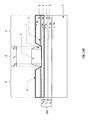
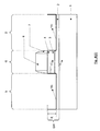
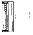
- Figure 1(A) represents schematically a cross section through a quantum well (QW) device according to the invention : (1)- substrate; (1a)- upper surface of the substrate; (S) - source region; (G) - gate region; (D)-drain region; (QW) -quantum well region; (2)- buffer structure; (2a)- upper surface of the buffer structure; (3)- channel structure; (3a)- upper surface of the channel structure; (4)- barrier layer; (4a)- upper surface of the barrier layer; (4')- barrier structure; (6)- gate electrode; (7)- first pair of insulating sidewall spacers; (8)- semiconductor material with a fourth band gap; (8a)-upper surface of the semiconductor material (8); (9)- ⁇ -doping layer.
- QW quantum well
- Figure 1(B) represents schematically the device of Figure 1(A) , further comprising (5) - gate oxide.
- Figure 1(C) represents schematically the device of Figure 1(A) , further comprising (10, 10') - S/D ohmic contacts.
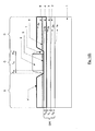
- Figure 2 (A) represents schematically the device of Figure 1(A) , wherein the ⁇ -doping layer (9) is replaced by a uniformly doped region (11) in the semiconductor material (8); (11a) - upper surface of the semiconductor material comprising the uniformly doped region (11); (11b) - lateral (faceted) surface of the semiconductor material comprising the uniformly doped region (11).
- Figure 2(B) represents schematically the device of Figure 2(A) , further comprising S/D ohmic contacts (10, 10').
- Figure 2(C) represents schematically the device of Figure 2(A) , further comprising self-aligned S/D contacts (13, 13') overlying the upper surface (11a) of the semiconductor material comprising the uniformly doped region (11); (15)- second pair of insulating sidewall spacers.
- Figure 3 (A) represents schematically the device of Figure 1(A) , wherein the ⁇ -doping layer (9) is replaced by a gradually doped region (12) in the semiconductor material (8); (12a) - upper surface of the semiconductor material comprising the gradually doped region (12); (12b) - lateral (faceted) surface of the semiconductor material comprising the gradually doped region (12).
- Figure 3(B) represents schematically the device of Figure 3(A) , additionally comprising (10, 10') - S/D ohmic contacts (10, 10').
- Figure 3 (C) represents schematically the device of Figure 3(A) , additionally comprising self-aligned S/D contacts (13, 13') overlying the upper surface (12a) of the semiconductor material comprising the gradually doped region (12); (15)- second pair of insulating sidewall spacers.
- Figure 4(A) represents schematically a cross section through a QW device comprising recessed S/D regions; (14c)- bottom surface of the recessed S/D regions;
- Figure 4(B) represents schematically a cross section through a QW device comprising recessed S/D regions filled with a re-grown doped semiconductor material (14); (14a)- upper surface of the re-grown doped semiconductor material (14); (14b)- lateral (faceted) surface of the re-grown semiconductor material; (10, 10') - S/D ohmic contacts.
- Figure 4(C) represents schematically the device of Figure 4(B) without S/D ohmic contacts, additionally comprising self-aligned S/D contacts (13, 13') overlying the upper surface (14a) of the re-grown doped semiconductor material (14); (15)- second pair of insulating sidewall spacers.
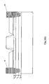
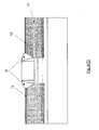
- Figure 5 represents schematically a hybrid QW device comprising a HEMT III-V QW device (I) as described in any of the embodiments represented in Figs 1 to 4 and a HHMT Ge-channel QW device (II), wherein: (1) - substrate; (2-1,2-11)- buffer structure; (3-I,3-II) - channel structure; (4-1,4-11) - barrier layer; (11-I, 11-II)-selectively-grown S/D regions comprising a doped region; (16)- shallow trench isolation (STI) oxide.
- STI shallow trench isolation
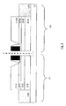
- Figure 6 represents schematically the simulated QW device (a) HEMT structure with continuous ⁇ -doping layer; (b) HEMT with interrupted ⁇ -doping layer according to the invention; (c) HEMT with interrupted ⁇ -doping layer and scaled EOT (Equivalent Oxide Thickness), according to the invention.
- EOT Equivalent Oxide Thickness
- DIBL Drain Induced Barrier Lowering
- SS subthreshold slope
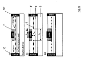
- Figure 10 represents the results of the simulations of the drive current as function of the length of the ⁇ -doping interruption (the spacers width); (b) represents the structure without a gate used to perform the simulations shown in graph 10(a).
- Field effect devices such as field effect transistors (FET) are basic components in most digital and many analog circuits, including circuits for data processing and telecommunications.
- FET field effect transistors
- Field effect devices typically comprise a conductive path between a source region and a drain region.
- n-channel depletion-mode device when no voltage is applied to the gate, current can flow from the source through the channel to the drain. If a sufficient negative voltage is applied to the gate, the channel region is depleted of carriers and the source-drain current is reduced or completely cut-off.
- n-channel enhancement-mode device when a positive gate to source voltage is applied, a conductive channel is created within the transistor. The positive voltage attracts free-floating electrons within the body towards the gate, forming a conductive channel.
- CMOS is a typical example of an enhancement-mode device, while in the case of HEMT both operating modes are possible.
- the operating frequency (the speed of such a device when employed as a switch) is determined by the length the gate-channel region.
- the requirement for higher operating frequencies together with the requirement for enhanced device density on a chip is the determining factor for device scaling.
- a HEMT High Electron Mobility Transistor
- a field effect transistor incorporating a junction between two materials with different band gaps (i.e. a heterojunction or heterostructure) as channel instead of a doped region, as is generally the case for MOSFETs.
- a commonly used material combination is GaAs with AlGaAs, though there is wide variation, dependent on the application of the device.
- HEMT High mobility electrons generated using the heterojunction of a highly-doped wide-bandgap n-type donor-supply layer (e.g. AlGaAs) and a non-doped narrow-bandgap channel layer (e.g. GaAs).
- a highly-doped wide-bandgap n-type donor-supply layer e.g. AlGaAs
- a non-doped narrow-bandgap channel layer e.g. GaAs
- the electrons generated in the n-type AlGaAs thin layer drop completely into the channel layer (GaAs), because the heterojunction created by different band-gap materials forms a quantum well (QW) in the conduction band on the GaAs side, where the electrons can move quickly without colliding with any impurities.
- QW quantum well
- the effect of this phenomenon is a very thin layer of highly mobile conducting electrons with very high concentration, giving the channel low resistivity (or high electron mobility).
- This layer is also known as a two-dimensional electron gas (2-DEG).
- 2-DEG two-dimensional electron gas
- a voltage applied to the gate electrode alters the conductivity of this layer.
- the material may include non-stoichiometric variations of the stoichiometrically exact formula identified by the chemical name. Lack of numerical subscript by an element in the formula stoichiometrically signifies the number one (1). Variations in the range plus/minus 20% of the exact stoichiometric number are comprised in the chemical name or formula, for the present purposes. Where an algebraic subscript is given, then variations in the range of about plus/minus 20% are comprised relative to the value of each subscript. Such varied values do not necessarily sum to a whole number and this departure is contemplated. Such variations may occur due to either intended selection and control of the process conditions, or due to unintended process variations.
- the term 'III-V compound semiconductor' denotes a semiconductor material that includes at least one element from Group III of the Periodic Table of Elements and at least one element from Group V of the Periodic Table of Elements.
- the III-V compound semiconductors are binary, ternary or quaternary alloys including III/V elements.
- III-V compound semiconductors that can be used in the present invention include, but are not limited to alloys of GaAs, InP, InSb, InGaAs, AlGaAs, InAIAs, InAlAsSb, InAlAsP and InGaAsP.
- a wide band gap (WBG) semiconductor is a semiconductor material with an electronic band gap larger than 1eV and, preferably, larger than 2eV.
- a narrow band gap (NBG) semiconductor is a semiconductor material with an electronic band gap smaller than 1eV and, preferably, smaller than 0.6 eV.
- WBG wide band gap
- NBG narrow band gap
- semiconductor denotes a material with a resistivity of about 10 5 ⁇ .cm (e.g. intrinsic Si has a resistivity of about 240 k ⁇ .cm), while a “semi-insulator” denotes a material with a higher resistivity value, of about 10 9 ⁇ .cm.
- the dielectric material having a dielectric constant of greater than 3.9 (k value of SiO 2 ) is referred to herein as a high-k dielectric.
- a high-k dielectric has a dielectric constant of about 7.0 or greater, with a dielectric constant of about 10.0 or greater being even more typical.
- a two dimensional electron gas 2-DEG
- the electrons are supplied by a ⁇ - doping layer (containing donor species) in the adjacent barrier layer/structure (see fig. 6a ).
- the invention is related to scalable quantum well (QW) devices and methods of manufacturing the same. Described in the most general way, the device of the invention is a quantum well device comprising :
- Various embodiments of the present invention disclose a device comprising an un-doped barrier layer and a doping layer/doped region comprised in the self-aligned source/drain regions adjacent to the gate region, the gate/source/drain regions overlying said barrier layer.
- shallow self-aligned source and drain contacts are formed on the upper surface of the source and drain regions.
- the source to drain spacing is reduced, being equal with the sum of the gate length and the insulating sidewall spacer width on both sides of the gate. Therefore, the very compact, self-aligned design is suitable for scaling and is an advantage of the present invention since it allows reducing the device capacitance and consequently, increasing the operating frequency.
- Another advantage is that by interrupting the ⁇ -doping layer (or the doped region, as shown further) and placing it outside the barrier layer, the thickness of the barrier layer can be scaled further towards lower values (lower EOT), suitable for gate lengths below 100nm. This is not possible in a classical HEMT structure where a ⁇ -doping layer is present between the gate and the QW structure, preventing the barrier thickness to be further reduced/scaled.
- a quantum well device comprising a substrate (1), a quantum well region (QW) overlying the substrate, a gate region (G) overlying the quantum well region, a source region (S) and a drain region (D) adjacent to the gate region, wherein
- the quantum well region (QW), as defined in the embodiment of figure 1 comprises three structures: the buffer structure (2), the channel structure (3) and the barrier layer (4). Each of these structures can comprise one or more layers.
- the buffer structure (2) comprises a semiconductor or semi-insulator material having a first band gap, wherein the first band gap is wider than the second band gap of the semiconductor material used to fabricate the channel structure (3).
- the semiconductor/semi-insulator material having a first band gap is a wide band gap (WBG) material, as defined elsewhere in the text.
- the buffer structure (2) can comprise multiple layers, each of the layers consisting of a semiconductor or semi-insulator material with a wide band gap.
- the channel structure (3) comprises an un-doped semiconductor material having a second band gap, wherein the second band gap is narrower than the first and the third band gap of the semiconductor material used to fabricate the buffer (2) and the barrier (4) structure, respectively.
- the semiconductor material having a second band gap is a narrow band gap (NBG) semiconductor material, as defined elsewhere in the text.
- the channel structure (3) can comprise multiple layers, each of the layers consisting of a semiconductor material with a narrow band gap.
- the channel structure can comprise three layers, a bottom layer overlying and in contact with the buffer structure (2), a top layer underlying and in contact with the barrier layer (4) and a mid layer sandwiched in between the bottom and the top layers.
- Each of the top and the bottom layers comprises a material selected to minimize the interface defects, while the mid layer comprises a material selected to enhance the mobility.
- a gradual doping with Indium e.g. a stack comprising InGaAs/InAs/InGaAs
- the channel structure/layer (3) has a thickness (h c , Figure 1(A) ) of about 3 to 20nm.
- the channel structure/layer has a thickness of 7nm.
- the barrier layer (4) comprises an un-doped semiconductor material having a third band gap, wherein the third band gap is wider than the second band gap of the semiconductor material used to fabricate the channel structure/layer (2).
- the semiconductor material having a third band gap is a wide band gap (WBG) semiconductor material, as defined elsewhere in the text.
- WBG wide band gap
- the barrier layer 4 can comprise multiple layers, each of the layers consisting of a semiconductor material with a wide band gap.
- the barrier layer is very thin (1-20 monolayers), made of an un-doped (i.e. no deliberate addition of doping, see above) semiconductor material and perfectly lattice matched with the underlying channel structure.
- a thin, un-doped and lattice matched barrier layer allows good control over the channel structure, minimizes the interface scattering at the interface with the gate electrode and preserves the transport properties of the carriers in the channel.
- the barrier layer 4 has a thickness (h sp in Figure 1(A) ) between 0.3 nm and 2 nm.
- the gate region (G) comprises a gate electrode (6) overlying the barrier layer (4) and a first pair of insulating sidewall spacers (7) on both sides of the patterned gate electrode.
- the dimensions of the gate region correspond to the combined dimensions of the gate electrode and the spacers.
- Patterning a gate electrode first, followed by forming self-aligned source and drain regions comprising a doping layer/region has the advantage of reduced overlap gate-source/drain capacitance and low resistance in the source/drain regions. By lowering the gate to source/drain overlap capacitance the switching speed of the device is improved.
- the first pair of insulating sidewall spacers are preventing the dopants from the doping layer/region comprised in the S/D regions to diffuse under the gate region.
- the dopants may diffuse in the underlying barrier layer under the source and drain region.
- the thickness of the insulating sidewall spacer is lower or equal to 5 nm and, more preferably, lower or equal with 4 nm.
- the doped region consists of a doping layer (9).
- the doping layer can be a delta-doping layer, consisting of at least 1 monolayer of dopants.
- the doped region is uniformly doped (11) as shown in Figure 2(A) .
- the doped region is gradually doped (12) with dopants, with the highest dopants concentration at the upper surface (12a) as shown in Figure 3(A) .
- the source region (S) and the drain region (D) are recessed regions defined in the quantum well region (QW) as shown in Figure 4(A) .
- the depth of the recess (d r ) is higher than the distance from the top edge of the recess (corresponding to the upper surface of the QW region) to the upper surface of the channel structure (3a) and lower than the distance from the top edge of the recess to the bottom surface of buffer structure (1a).
- the gate region (G) comprises further a gate dielectric (5) sandwiched in between the barrier layer (4) and the gate electrode (6), as shown in Figure 1(B) .
- the presence of the gate dielectric improves the QW device performance by reducing the gate leakage.
- the gate dielectric (5) comprises a high-k dielectric.
- the high-k dielectric employed in the present invention includes, but is not limited to an oxide, nitride, oxynitride and/or silicates including metal silicates, aluminates, titanates and nitrides.
- the high-k dielectric can comprise HfO 2 , HfSiO, ZrO 2 , Al 2 O 3 , TiO 2 , Lanthanide-based oxides (i.e. La 2 O 3 , GdGaO), Y 2 O 3 , Ga 2 O 3 , perovskites (i.e. SrTiO 3 ) or combinations thereof.
- the gate region of the QW device can comprise a passivation layer (not shown) underlying the high-k material (5), wherein the passivation layer can be formed by performing a pre-treatment (cleaning/UV- exposure/short deposition step) on the barrier layer (4).
- the QW device comprises further a second pair of insulating sidewall spacers (15) overlying any faceted regions (11b, 12b, 14b) of the self aligned source and drain regions near the gate edge and self-aligned source and drain shallow contacts (13, 13'), overlying the upper surface (8a, 11a, 12a, 14a) of respectively the source region (S) and the drain region (D).
- the self aligned source and drain shallow contacts (13, 13') comprise a metal silicide or a metal germanide or a metal-III-V compound.
- the shallow contacts have the advantage of lower source and drain resistance, increasing in this way the operational speed of the QW device.
- the shallow contacts are suitable options for scaling.
- the QW device comprises further source and drain ohmic contacts (10, 10') as shown in Figures 1(C) , 2(B) , 3(B) , 4(B) , 6(b) and 6(c) .
- the ohmic contacts can comprise a metal, an alloyed metal, metal nitride or a metal silicide/germanide.
- the ohmic contacts can comprise W, Al, Ti, Ta, Pt or Au-based alloys like NiAuGe.
- the semiconductor material with the first band gap, the semiconductor material with the third band gap and the semiconductor material with the fourth band gap are wide band gap semiconductors (WBG).
- WBG wide band gap semiconductors
- the fourth band gap may be still wider than the third band gap.
- the WBG semiconductor material is selected from the group consisting of AlGaAs, AlGaSb, GaInP and combinations thereof.
- the WBG semiconductor material is Si 1-x Ge x , where x is a real number between 0 and 0.7, more preferably between 0 and 0.5.
- the WBG semiconductor material is selected from the group consisting of GaN, AlGaN, AlN and related materials having electronic band gaps above 3 eV.
- GaN, AlGaN, AlN as WBG materials in combination with Ge as NBG material has the additional advantage of employing established techniques for growing/depositing good quality layers and interfaces.
- the semiconductor material with the second band gap is narrow band gap semiconductor (NBG).
- the NBG semiconductor material is selected from the group consisting of InGaAs, InGaSb, InAs, InAsP, InAsSb and combinations thereof.
- the NBG semiconductor material is Si 1-y Ge y , where y is a real number between 0.3 and 1, more preferably between 0.5 and 1.
- the WBG semiconductor material is Si 1-x Ge x , where x is a real number between 0 and 0.7 and the NBG semiconductor material is Si 1-y Ge y , where y is a real number between 0.3 and 1 and where y > x.
- the doped region comprises dopants.
- the dopants can be a n-type dopant (donor species) or a p-type dopant. More particularly the donor species can be Si.
- the dopants can be selected from the group consisting of B, As, P, Sb, Ga and combinations thereof.
- the doped region can be a doping layer (9), or a uniformly doped region (11, 14), or a gradually doped region (12, 14) as illustrated in Figure 1(A) , 2(A) and 3(A) , respectively.
- the thickness of the doping layer can be lower than 3 nm and, more preferably, lower than 1nm.
- the doping layer can be positioned anywhere in the self-aligned source and drain region, more preferably close to the interface with the barrier layer (4).
- the concentration of the donor species/dopants in the doping layer is from 10 11 to 10 13 atoms.cm -2 . More preferably the concentration of the donor species/dopants in the doping layer is higher than 10 12 atoms.cm -2 , or even more preferably higher than 5.10 12 atoms.cm -2 .
- the high doping level of the source and drain regions improves further the source and drain resistance.
- the concentration of dopants can range from 10 17 to 10 21 atoms.cm -3 . More preferably, the concentration of dopants can vary between 10 18 to 2.10 20 atoms.cm -3 .
- the highest concentration of dopants a value at the upper end of the range mentioned in the preceding paragraph for the uniformly doped region (e.g. 2.10 20 atoms.cm -3 ), is located at the upper surface of the source/drain regions.
- the substrate (1) can be a bulk semiconductor substrate or a material stack comprising at least a semiconductor substrate. More preferably, the substrate (1) comprises Si, Ge, SiGe, Silicon on Insulator (SOI), Germanium on Insulator (GOI), GaAs.
- SOI Silicon on Insulator
- GOI Germanium on Insulator
- the gate electrode (6) can comprise a conductive material like e.g. a metal, a metal alloy, a metal silicide, metal nitrides, a metal germanide, poly-silicon (poly_Si), poly-silicon-germanium and any combinations or multilayers thereof.
- the gate conductor is a metal comprising at least one of the elements Al, Au, W or Ti.
- a NFET quantum well device comprising a substrate (1), a quantum well region (QW) overlying the substrate, a gate region (G) overlying the quantum well region, a source region (S) and a drain region (D) adjacent to the gate region, wherein
- a hybrid device comprising a NFET (HEMT) quantum well device (I) as described in any of the preceding embodiments and a PFET (HHMT, High Hole Mobility Transistor) quantum well device (II) comprising a Ge-channel structure.
- HEMT NFET
- HHMT High Hole Mobility Transistor
- the QW region of the HEMT device (I) comprises a buffer structure (2-I) comprising or consisting of GaAs, a channel structure (3-I) comprising or consisting of strained InGaAs and a barrier layer (4-I) comprising or consisting of InGaAlAs or InP.
- the self-aligned S/D regions (11) of the HEMT are selectively grown and comprise or consist of n-doped GaAs.
- the QW region of the HHMT device (II) comprises a buffer structure (2-II) comprising or consisting of SiGe, a channel structure (3-II) comprising or consisting of strained Ge and a barrier layer (4-II) comprising or consisting of a Si passivation layer.
- the self-aligned S/D regions (11') of the HHMT are selectively grown and comprise or consist of p-doped SiGe. Both devices are integrated on an e.g. Si substrate (1) and separated by shallow trench isolations (16).
- the present invention also relates to a method of fabricating such quantum well devices.
- a method for producing a quantum well device is disclosed comprising
- a method for manufacturing a quantum well device with self-aligned source/drain regions comprising
- forming the gate region (G) further comprises forming a gate electrode (6) overlying a portion of the barrier layer (4) and forming a first pair of insulating sidewall spacers (7) on both sides of the gate electrode (6) as illustrated in Fig 1(A) .
- Forming the gate electrode (6) comprises depositing a layer or a multi-layer of a conductive material (gate electrode) overlying the barrier layer (4) and the lithographic patterning of the gate electrode using a photoresist material.
- a hard-mask layer comprising e.g. Si-oxide or Si-nitride, can be interposed in between the gate electrode and the photoresist material.
- gate lengths (L g ) below 50nm and, more preferably, below 25nm are used.
- the gate electrode (6) can be formed by a replacement gate process (not shown).
- the replacement gate process may consist in a damascene like processing, comprising multiple steps: forming a sacrificial gate electrode in a 'gate first' process, encapsulating the gate electrode with insulating sidewall spacers, removing the sacrificial gate electrode, filling up the trench left by the selective removal of the sacrificial gate with the gate electrode material (i.e. metal), performing a chemical mechanical polishing (CMP) step.
- CMP chemical mechanical polishing
- Forming a first pair of insulating sidewall spacers comprises depositing a layer of insulating material (e.g. Si-oxide, Si-nitride) and afterwards patterning the spacers (e.g. removing anisotropically the insulating material from the upper surface of the gate region and the source/drain regions selectively towards the underlying materials), such as insulating sidewall spacers (7) are formed on both sides of the gate electrode (6).
- insulating material e.g. Si-oxide, Si-nitride
- the width of the insulating sidewall spacers (w ox ) is lower or equal to 10nm, more preferred lower or equal to 5nm, on each side of the gate electrode.
- the minimum width/thickness is determined by the requirement to have a good insulation between the gate and the source/drain regions.
- the optimum width/thickness of the insulating sidewall spacers is determined, as shown by the simulations in Example 1 and Fig 10 (a) and (b) by the maximum interruption in the ⁇ -doping layer which does not have an influence on the channel doping, i.e. the series resistance R s of the QW device.
- the method further comprises, after the selective growth of the self-aligned source (S) and the drain (D) regions, forming a second pair of insulating sidewall spacers (15) overlying any faceted regions of the selectively grown source and drain regions near the gate edge (11b, 12b, 14b), and thereafter forming shallow self-aligned source and drain contacts (13, 13').
- S self-aligned source
- D drain
- FIG. 2(C) , 3(C) and 4(C) are illustrated in Figures 2(C) , 3(C) and 4(C) .
- the process of forming shallow self-aligned source and drain contacts involves the steps of depositing a thin metal layer overlying the source, drain and gate region, thereafter performing a thermal treatment, whereby the thin metal layer reacts with a superficial layer of the semiconductor material (11, 12, 14) at the upper surface of the source and the drain region (11a, 12a, 14a) forming a metal compound (e.g. a silicide, a germanide, a III-V metal compound), followed by removing selectively the un-reacted metal towards the metal-compound.
- a metal compound e.g. a silicide, a germanide, a III-V metal compound
- Selective growth of the source and the drain regions can be performed by selective epitaxial growth (SEG) techniques.
- SEG selective epitaxial growth
- faceting of the epitaxial grown material can occur near i.e. the insulating sidewall spacers. This faceting causes the thickness of the elevated source/drain regions to be thinner near the edge of the insulating material resulting in device fabrication concerns.
- S/D shallow contacts siliconcidation, germanidation
- local shorts can be formed between the S/D region and the gate region.
- a second pair of insulating sidewall spacers (15) are formed after the selective epitaxial growth.
- the doped region (9, 11, 12, 14) is formed by in-situ doping during the selective epitaxial growth.
- the doped region (9, 11, 12, 14) is formed by implantation after the selective epitaxial growth.
- the method to manufacture a QW device further comprises, after forming the gate region (G), forming recessed source and drains regions in the quantum well region (QW), by etching recesses on both sides of the gate region as shown in Figure 4(A) .
- the recess depth (d r ) is higher than the distance from the edge of the recess to the upper surface of the channel structure (3a) and lower than the distance from the edge of the recess to the bottom surface of buffer structure (1a).
- the method further comprises patterning a gate dielectric (5) sandwiched in between the barrier layer (4) and the gate electrode (6) in the gate region (G) as shown in Figure 1(B) .
- the gate region of the QW device can comprise a passivation layer (not shown) underlying the high-k material (5), wherein the passivation layer can be formed by e.g. performing a pre-treatment (cleaning/UV exposure/short deposition step) on the barrier layer
- a method for manufacturing a NFET quantum well device comprising
- the structures comprised in the QW region are deposited using an epitaxial deposition technique such as molecular beam epitaxy (MBE), metal-organic chemical vapor deposition (MOCVD), Metal-organic Vapor Phase Epitaxy (MOVPE) Low-Pressure Chemical Vapor Deposition (LPCVD), Ultra High Vacuum Chemical Vapor Deposition (UHV CVD) or Atmospheric Pressure Chemical Vapor Deposition (APCVD).
- MBE molecular beam epitaxy
- MOCVD metal-organic chemical vapor deposition
- MOVPE Metal-organic Vapor Phase Epitaxy
- LPCVD Low-Pressure Chemical Vapor Deposition
- UHV CVD Ultra High Vacuum Chemical Vapor Deposition
- APCVD Atmospheric Pressure Chemical Vapor Deposition
- the semiconductor materials comprised in the source/drain regions and in the re-grown source/drain regions are formed by selective deposition/growth.
- selective growth techniques include but are not limited to
- a method to manufacture a hybrid QW device comprises a HEMT device (I) having a III-V channel structure and a HHMT device (II) having a Ge channel structure formed on a Si-substrate by using a Si-compatible, gate-first process flow.
- the Si-compatible process flow comprises the following steps:
- This example shows that the delta ( ⁇ ) doping layer under the gate of a high electron mobility transistor can be removed for a 10 nm gate.
- the resulting V T shift can be countered by increasing the sheet charge in the ⁇ -doping layer.
- the removal of the ⁇ -doping layer allows to reduce the barrier thickness under the gate, resulting in increased gate control.
- Figure 6(b) presents an alternative HEMT structure, where the ⁇ -doping layer is interrupted over a length L ⁇ .
- Figure 6(c) shows another alternative HEMT structure, where the ⁇ -doping layer is interrupted over a length L ⁇ and the EOT is lowered/reduced.
- the length of the interruption L ⁇ is equal to the sum of the gate length (Lg) and the insulating (oxide) spacers width (w ox ) on both sides of the gate.
- the analysis of the alternative HEMT is based on five structures.
- the first one is a classical HEMT reference.
- Structure A is identical to the reference structure, except for an interruption of 18 nm in the ⁇ -doping layer.
- the resulting V T shift (as explained in the following paragraph) is compensated by increasing the ⁇ -doping sheet charge in structure B.
- structures C and D explore the effect of moving the gate closer to the channel (reducing the barrier thickness h sp ), a possibility created by the removal of the ⁇ -doping under the gate. Table 1 lists the important parameters for the investigated structures.
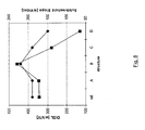
- the (linear) V T for each structure, extracted with the max-g m method, is included in the legend.
- the reference HEMT has a V T of -0.19V. Removing the ⁇ -doping layer under the gate and spacers (structure A) results in a V T increase of 350mV. Lowering EOT in combination with removing the ⁇ -doping layer results in a further V T increase (e.g. 430mV for structure D with respect to the reference).
- the device with structure D functions in enhancement mode. This can be understood by considering that an interruption of the ⁇ -doping layer reduces the charge in the QW-channel.
- the advantage of an interruption in the ⁇ -doping layer is that it allows further scaling of the spacing between the gate and the QW-channel (barrier thickness, h sp ). As shown in Figure 7 , decreasing h sp to 7 or 4 nm (structures C and D) clearly leads to better gate control in the subthreshold region.
- the subtreshold slope varies from 150mv/dec in case of the reference structure, to 110mV/dec for structure D with interrupted ⁇ -doping and scaled EOT. This becomes even more obvious when looking at short channel effects in Figure 8 .
- DIBL is a measure of the change in the treshold voltage V T of the device as a result of change in V DS . Small DIBL values reflect a good V T stability to manufacturing variations.
- DIBL and subthreshold slope give a measure of the overall electrostatic integrity of the device.
- DIBL and subthreshold slope (SS) are significantly improved for the structures with reduced barrier thickness, h sp (C and D).
- the ⁇ -doping layer has a sheet charge of 3.10 12 atoms .cm -2 and the insulator sidewall spacers have a width of 4nm on each side of the gate.
- I on is determined by the gate channel functioning in accumulation mode, while the I off is determined by depletion and the interrupted doping.
- there is no penalty in I on for L g ⁇ 150 nm which confirms that for device architectures with interrupted doping layer the L g is not a critical design factor.
- Figure 10 (a) represents the results of the simulations for the optimum spacer thickness/width.
- the effect of various spacer thicknesses was simulated with a device without a gate (only with an interrupted doping) as the structure represented in Figure 10 (b) .
Claims (11)
- Quantentopfvorrichtung, umfassend:- ein Substrat (1),- eine das Substrat (1) überlagernde und kontaktierende Pufferstruktur (2), wobei die Pufferstruktur ein Halbleitermaterial mit einer ersten Bandlücke umfasst,- eine die Pufferstruktur (2) überlagernde und kontaktierende Kanalstruktur (3), umfassend ein Halbleitermaterial mit einer zweiten Bandlücke,- eine die Kanalstruktur (3) überlagernde und kontaktierende Barrierestruktur (4'), umfassend ein Halbleitermaterial mit einer dritten Bandlücke, und ferner umfassend einen zur Bildung eines 2-dimensionalen Trägergases geeigneten Dotierstoff,- eine einen Teil der Barrierestruktur überlagernde Gate-Region (G), umfassend eine Gate-Elektrode (6),- Source- und Drainkontakte (10, 10', 13, 13'),wobei die erste und dritte Bandlücke breiter sind als die zweite Bandlücke,
und wobei im unterhalb der Gate-Region angeordneten Teil der Barrierestruktur kein Dotierstoff vorhanden ist, wobei die Barrierestruktur (4') umfasst:- eine die Kanalstruktur überlagernde und kontaktierende Barriereschicht (4), umfassend ein nicht dotiertes Halbleitermaterial mit der dritten Bandlücke, wobei die Pufferstruktur, Kanalstruktur und Barriereschicht gemeinsam eine Quantentopfregion (QW) bilden, und- eine Source-Region (S) und eine Drain-Region (D), die an die Gate-Region grenzen, wobei die Source- und Drain-Regionen jeweils selbsttätig an der Gate-Region (G) ausgerichtet sind und wobei die Source- und Drain-Regionen ein Halbleitermaterial (8) mit einer vierten Bandlücke und eine aus dem Dotierstoff ausgebildete dotierte Region umfassen, wobei die vierte Bandlücke breiter ist als die zweite Bandlücke,wobei die Gate-Region (G) eine Gate-Elektrode (6), die einen Teil der Barrierestruktur (4') überlagert, und ein erstes Paar isolierender Seitenwand-Abstandhalter (7) umfasst, dadurch gekennzeichnet, dass die Barriereschicht (4) eine Stärke zwischen 0,3 nm und 2 nm aufweist. - Vorrichtung nach Anspruch 1, wobei die dotierte Region aus einer Delta-Dotierschicht (9) besteht.
- Vorrichtung nach Anspruch 1, wobei die dotierte Region einheitlich dotiert ist (11).
- Vorrichtung nach Anspruch 1, wobei die dotierte Region stufenweise dotiert ist (12), wobei die höchste Dotierstoffkonzentration auf der oberen Fläche (12 a) liegt.
- Vorrichtung nach einem der Ansprüche 1 bis 4, wobei die Breite jedes insulierenden Seitenwand-Abstandhalters weniger oder gleich 5 nm beträgt.
- Vorrichtung nach einem der Ansprüche 1 bis 5, wobei die Source- (S) und Drain-Region (D) vertiefte Regionen sind, die durch eine Vertiefung der Quantentopfregion (QW) definiert sind, und wobei die Tiefe (dr) der Vertiefung größer ist als der Abstand vom Rand der Vertiefung zur oberen Fläche der Kanalstruktur (3a) und kleiner ist als der Abstand vom Rand der Vertiefung zur unteren Fläche der Pufferstruktur (1 a).
- Vorrichtung nach einem der Ansprüche 1 bis 6, ferner umfassend ein zwischen Barriereschicht (4) und Gate-Elektrode (6) in der Gate-Region (G) sandwichartig angeordnetes Gate-Dielektrikum (5).
- Quantentopfvorrichtung nach Anspruch 1, wobei die Vorrichtung eine NFET-Quantentopfvorrichtung ist, und wobei die jeweiligen Halbleitermaterialien der Pufferstruktur, Kanalstruktur, Barriereschicht und Source- und Drain-Regionen III-V Verbindungshalbleitermaterialien sind.
- Verfahren zur Herstellung einer Quantentopfvorrichtung, umfassend- Vorsehen eines Substrats (1),- Bilden einer Quantentopfregion (QW), umfassend die nachfolgenden Schrittewobei die erste und dritte Bandlücke breiter sind als die zweite Bandlücke, und- Bilden einer Pufferstruktur (2) durch Epitaxialwachstum, wobei die Pufferstruktur das Substrat (1) überlagert und ein Halbleitermaterial mit einer ersten Bandlücke umfasst,- Bilden einer Kanalstruktur (3) durch Epitaxialwachstum, die die Pufferstruktur (2) überlagert und ein Halbleitermaterial mit einer zweiten Bandlücke umfasst,- Bilden einer Barriereschicht (4) durch Epitaxialwachstum, die die Kanalstruktur (3) überlagert und ein nicht dotiertes Halbleitermaterial mit einer dritten Bandlücke umfasst,- Bilden einer Gate-Region (G), die einen Teil der Quantentopfregion (QW) überlagert, und- Bilden einer Source-Region (S) und einer Drain-Region (D), die selbsttätig an der Gate-Region (G) ausgerichtet sind, durch selektives Wachstum eines Halbleitermaterials (8) mit einer vierten Bandlücke, die breiter ist als die zweite Bandlücke, und wobei die Source- (S) und Drain-Regionen (D) jeweils eine dotierte Region umfassen, wobei die Bildung der Gate-Region (G) ferner umfasst- Bilden einer Gate-Elektrode (6), die einen Teil der Barrierestruktur (4') überlagert, und- Bilden eines ersten Paares isolierender Seitenwand-Abstandhalter (7) auf beiden Seiten der Gate-Elektrode (6).
- Verfahren nach Anspruch 9, ferner umfassend, nach der Bildung der Gate-Region (G), Bilden vertiefter Source- und Drain-Regionen in der Quantentopfregion (QW), durch Einätzen von Vertiefungen auf beiden Seiten der Gate-Region mit einer Tiefe (dr), die größer ist als der Abstand vom Rand der Vertiefung zur oberen Fläche der Kanalstruktur (3a) und kleiner ist als der Abstand vom Rand der Vertiefung zur unteren Fläche der Pufferstruktur (1a).
- Verfahren nach Anspruch 9, wobei die Quantentopfvorrichtung eine NFET-Quantentopfvorrichtung ist, und wobei die jeweiligen Halbleitermaterialien der Pufferstruktur, Kanalstruktur, Barriereschicht und Source- und Drain-Regionen III-V Verbindungshalbleitermaterialien sind.
Priority Applications (3)
| Application Number | Priority Date | Filing Date | Title |
|---|---|---|---|
| US12/463,338 US7915608B2 (en) | 2008-05-13 | 2009-05-08 | Scalable quantum well device and method for manufacturing the same |
| JP2009116320A JP5669365B2 (ja) | 2008-05-13 | 2009-05-13 | 小型化可能な量子井戸デバイスおよびその製造方法 |
| US13/034,592 US8119488B2 (en) | 2008-05-13 | 2011-02-24 | Scalable quantum well device and method for manufacturing the same |
Applications Claiming Priority (1)
| Application Number | Priority Date | Filing Date | Title |
|---|---|---|---|
| US5286908P | 2008-05-13 | 2008-05-13 |
Publications (2)
| Publication Number | Publication Date |
|---|---|
| EP2120266A1 EP2120266A1 (de) | 2009-11-18 |
| EP2120266B1 true EP2120266B1 (de) | 2015-10-28 |
Family
ID=40727126
Family Applications (1)
| Application Number | Title | Priority Date | Filing Date |
|---|---|---|---|
| EP08168648.7A Not-in-force EP2120266B1 (de) | 2008-05-13 | 2008-11-07 | Skalierbare Quantentopfvorrichtung und Verfahren zu deren Herstellung |
Country Status (3)
| Country | Link |
|---|---|
| US (2) | US7915608B2 (de) |
| EP (1) | EP2120266B1 (de) |
| JP (1) | JP5669365B2 (de) |
Families Citing this family (48)
| Publication number | Priority date | Publication date | Assignee | Title |
|---|---|---|---|---|
| JP2010135640A (ja) * | 2008-12-05 | 2010-06-17 | Panasonic Corp | 電界効果トランジスタ |
| US7759142B1 (en) * | 2008-12-31 | 2010-07-20 | Intel Corporation | Quantum well MOSFET channels having uni-axial strain caused by metal source/drains, and conformal regrowth source/drains |
| US20100314610A1 (en) * | 2009-04-10 | 2010-12-16 | Mil Shtein Samson | Hemt with improved quantum confinement of electrons |
| JP2011077516A (ja) * | 2009-09-07 | 2011-04-14 | Sumitomo Chemical Co Ltd | 電界効果トランジスタ、半導体基板及び電界効果トランジスタの製造方法 |
| US8368052B2 (en) | 2009-12-23 | 2013-02-05 | Intel Corporation | Techniques for forming contacts to quantum well transistors |
| US8324661B2 (en) * | 2009-12-23 | 2012-12-04 | Intel Corporation | Quantum well transistors with remote counter doping |
| US8253167B2 (en) * | 2010-01-26 | 2012-08-28 | Taiwan Semiconductor Manufacturing Company, Ltd. | Method for forming antimony-based FETs monolithically |
| US8907350B2 (en) | 2010-04-28 | 2014-12-09 | Cree, Inc. | Semiconductor devices having improved adhesion and methods of fabricating the same |
| KR101679054B1 (ko) * | 2010-05-04 | 2016-11-25 | 삼성전자주식회사 | 산소처리영역을 포함하는 고 전자 이동도 트랜지스터 및 그 제조방법 |
| US9449833B1 (en) | 2010-06-02 | 2016-09-20 | Hrl Laboratories, Llc | Methods of fabricating self-aligned FETS using multiple sidewall spacers |
| US8558281B1 (en) * | 2011-12-02 | 2013-10-15 | Hrl Laboratories, Llc | Gate metallization methods for self-aligned sidewall gate GaN HEMT |
| US8946724B1 (en) | 2010-06-02 | 2015-02-03 | Hrl Laboratories, Llc | Monolithically integrated self-aligned GaN-HEMTs and Schottky diodes and method of fabricating the same |
| US8878246B2 (en) | 2010-06-14 | 2014-11-04 | Samsung Electronics Co., Ltd. | High electron mobility transistors and methods of fabricating the same |
| CN101986435B (zh) * | 2010-06-25 | 2012-12-19 | 中国科学院上海微系统与信息技术研究所 | 防止浮体及自加热效应的mos器件结构的制造方法 |
| US20120161105A1 (en) * | 2010-12-22 | 2012-06-28 | Willy Rachmady | Uniaxially strained quantum well device and method of making same |
| US8431961B2 (en) | 2011-02-03 | 2013-04-30 | Micron Technology, Inc. | Memory devices with a connecting region having a band gap lower than a band gap of a body region |
| JP2012195579A (ja) * | 2011-03-02 | 2012-10-11 | Sumitomo Chemical Co Ltd | 半導体基板、電界効果トランジスタ、半導体基板の製造方法および電界効果トランジスタの製造方法 |
| US8610172B2 (en) | 2011-12-15 | 2013-12-17 | International Business Machines Corporation | FETs with hybrid channel materials |
| EP2608269A1 (de) * | 2011-12-23 | 2013-06-26 | Imec | Quantentopftransistor, Verfahren zur Herstellung solch eines Quantentopftransistors und Verwendung solch eines Quantentopftransistors |
| JP2013207020A (ja) * | 2012-03-28 | 2013-10-07 | Nippon Telegr & Teleph Corp <Ntt> | 電界効果トランジスタおよびその製造方法 |
| US8866195B2 (en) | 2012-07-06 | 2014-10-21 | Taiwan Semiconductor Manufacturing Co., Ltd. | III-V compound semiconductor device having metal contacts and method of making the same |
| US8916443B2 (en) * | 2012-06-27 | 2014-12-23 | International Business Machines Corporation | Semiconductor device with epitaxial source/drain facetting provided at the gate edge |
| US8748942B2 (en) | 2012-07-09 | 2014-06-10 | Taiwan Semiconductor Manufacturing Company, Ltd. | High electron mobility transistor and method of forming the same |
| EP2696369B1 (de) | 2012-08-10 | 2021-01-13 | IMEC vzw | Herstellungsverfahren für eine Feldeffekt-Halbleitervorrichtung |
| US9099490B2 (en) * | 2012-09-28 | 2015-08-04 | Intel Corporation | Self-aligned structures and methods for asymmetric GaN transistors and enhancement mode operation |
| US8877604B2 (en) * | 2012-12-17 | 2014-11-04 | International Business Machines Corporation | Device structure with increased contact area and reduced gate capacitance |
| CN103219944B (zh) * | 2013-04-23 | 2015-09-16 | 华南师范大学 | 一种基于低维半导体结构的倍频器 |
| US10867792B2 (en) * | 2014-02-18 | 2020-12-15 | Taiwan Semiconductor Manufacturing Company, Ltd. | High electron mobility transistor (HEMT) having an indium-containing layer and method of manufacturing the same |
| US9412836B2 (en) * | 2014-03-06 | 2016-08-09 | Taiwan Semiconductor Manufacturing Co., Ltd. | Contacts for transistors |
| US10553718B2 (en) | 2014-03-14 | 2020-02-04 | Taiwan Semiconductor Manufacturing Co., Ltd. | Semiconductor devices with core-shell structures |
| US9640656B2 (en) * | 2014-04-04 | 2017-05-02 | Micron Technology, Inc. | Transistors having strained channel under gate in a recess |
| US9812323B2 (en) | 2014-09-08 | 2017-11-07 | Internaitonal Business Machines Corporation | Low external resistance channels in III-V semiconductor devices |
| CN104810405B (zh) * | 2015-04-13 | 2018-07-13 | 北京大学 | 一种隧穿场效应晶体管及制备方法 |
| EP3284302B1 (de) * | 2015-04-13 | 2019-01-23 | Telefonaktiebolaget LM Ericsson (publ) | Verfahren zur reduzierung der unterbrechung einer versorgenden zelle aufgrund von prose-betrieb |
| WO2017105384A1 (en) * | 2015-12-14 | 2017-06-22 | Intel Corporation | Geometric manipulation of 2deg region in source/drain extension of gan transistor |
| US9941363B2 (en) | 2015-12-18 | 2018-04-10 | International Business Machines Corporation | III-V transistor device with self-aligned doped bottom barrier |
| US20170179232A1 (en) * | 2015-12-18 | 2017-06-22 | International Business Machines Corporation | Iii-v transistor device with doped bottom barrier |
| US10170611B1 (en) | 2016-06-24 | 2019-01-01 | Hrl Laboratories, Llc | T-gate field effect transistor with non-linear channel layer and/or gate foot face |
| US10510903B2 (en) | 2016-11-29 | 2019-12-17 | Taiwan Semiconductor Manufacturing Co., Ltd. | Impact ionization semiconductor device and manufacturing method thereof |
| US10868161B2 (en) | 2018-08-29 | 2020-12-15 | Qualcomm Incorporated | Low resistance source/drain regions in III-V transistors |
| US10868162B1 (en) | 2018-08-31 | 2020-12-15 | Hrl Laboratories, Llc | Self-aligned gallium nitride FinFET and method of fabricating the same |
| US10923493B2 (en) | 2018-09-06 | 2021-02-16 | Micron Technology, Inc. | Microelectronic devices, electronic systems, and related methods |
| JP7016311B2 (ja) * | 2018-11-06 | 2022-02-04 | 株式会社東芝 | 半導体装置 |
| CN110287541B (zh) * | 2019-05-29 | 2023-11-17 | 杭州电子科技大学 | 一种基于AgilentHBT模型III-V族HBT可缩放建模方法 |
| US20200395358A1 (en) * | 2019-06-17 | 2020-12-17 | Intel Corporation | Co-integration of extended-drain and self-aligned iii-n transistors on a single die |
| US11127820B2 (en) * | 2019-09-20 | 2021-09-21 | Microsoft Technology Licensing, Llc | Quantum well field-effect transistor and method for manufacturing the same |
| US20220376085A1 (en) * | 2021-05-20 | 2022-11-24 | Cree, Inc. | Methods of manufacturing high electron mobility transistors having improved performance |
| WO2023223499A1 (ja) * | 2022-05-19 | 2023-11-23 | 日本電信電話株式会社 | 半導体装置 |
Family Cites Families (15)
| Publication number | Priority date | Publication date | Assignee | Title |
|---|---|---|---|---|
| JPS6012775A (ja) * | 1983-07-02 | 1985-01-23 | Agency Of Ind Science & Technol | 電界効果トランジスタ |
| JP3173080B2 (ja) * | 1991-12-05 | 2001-06-04 | 日本電気株式会社 | 電界効果トランジスタ |
| JP3388189B2 (ja) * | 1998-09-14 | 2003-03-17 | 富士通株式会社 | 化合物半導体装置の製造方法 |
| JP4865189B2 (ja) * | 2002-02-21 | 2012-02-01 | 古河電気工業株式会社 | GaN系電界効果トランジスタ |
| JP3923400B2 (ja) * | 2002-09-27 | 2007-05-30 | 富士通株式会社 | 電界効果トランジスタおよびその製造方法 |
| JP2006190991A (ja) * | 2004-12-09 | 2006-07-20 | Matsushita Electric Ind Co Ltd | 電界効果トランジスタ及びその製造方法 |
| JP4895520B2 (ja) * | 2005-03-28 | 2012-03-14 | 日本電信電話株式会社 | ショットキーダイオードおよびその製造方法 |
| JP4730529B2 (ja) * | 2005-07-13 | 2011-07-20 | サンケン電気株式会社 | 電界効果トランジスタ |
| JP2007035905A (ja) * | 2005-07-27 | 2007-02-08 | Toshiba Corp | 窒化物半導体素子 |
| JP4751150B2 (ja) * | 2005-08-31 | 2011-08-17 | 株式会社東芝 | 窒化物系半導体装置 |
| JP2007150282A (ja) * | 2005-11-02 | 2007-06-14 | Sharp Corp | 電界効果トランジスタ |
| US9040398B2 (en) * | 2006-05-16 | 2015-05-26 | Cree, Inc. | Method of fabricating seminconductor devices including self aligned refractory contacts |
| EP1883115A1 (de) * | 2006-07-28 | 2008-01-30 | Interuniversitair Microelektronica Centrum (IMEC) | Feldefftektbauelement vom Anreicherungs-Typ und Verfahren zu seiner Herstellung |
| TW200830550A (en) * | 2006-08-18 | 2008-07-16 | Univ California | High breakdown enhancement mode gallium nitride based high electron mobility transistors with integrated slant field plate |
| JP2009099691A (ja) * | 2007-10-15 | 2009-05-07 | Sanken Electric Co Ltd | 電界効果半導体装置の製造方法 |
-
2008
- 2008-11-07 EP EP08168648.7A patent/EP2120266B1/de not_active Not-in-force
-
2009
- 2009-05-08 US US12/463,338 patent/US7915608B2/en not_active Expired - Fee Related
- 2009-05-13 JP JP2009116320A patent/JP5669365B2/ja not_active Expired - Fee Related
-
2011
- 2011-02-24 US US13/034,592 patent/US8119488B2/en not_active Expired - Fee Related
Also Published As
| Publication number | Publication date |
|---|---|
| US20110140087A1 (en) | 2011-06-16 |
| JP5669365B2 (ja) | 2015-02-12 |
| JP2010010663A (ja) | 2010-01-14 |
| US7915608B2 (en) | 2011-03-29 |
| US20090283756A1 (en) | 2009-11-19 |
| US8119488B2 (en) | 2012-02-21 |
| EP2120266A1 (de) | 2009-11-18 |
Similar Documents
| Publication | Publication Date | Title |
|---|---|---|
| EP2120266B1 (de) | Skalierbare Quantentopfvorrichtung und Verfahren zu deren Herstellung | |
| US10177249B2 (en) | Techniques for forming contacts to quantum well transistors | |
| US10141437B2 (en) | Extreme high mobility CMOS logic | |
| US8796733B2 (en) | Low voltage tunnel field-effect transistor (TFET) and method of making same | |
| US7964896B2 (en) | Buried channel MOSFET using III-V compound semiconductors and high k gate dielectrics | |
| US9666684B2 (en) | III-V semiconductor device having self-aligned contacts | |
| US9159822B2 (en) | III-V semiconductor device having self-aligned contacts | |
| US9853026B2 (en) | FinFET device and fabrication method thereof | |
| US9059267B1 (en) | III-V device with overlapped extension regions using replacement gate | |
| KR101772278B1 (ko) | 누설 전류 억제 방법 및 그 관련 구조물들 | |
| US9064946B1 (en) | III-V FET device with overlapped extension regions using gate last | |
| US9312128B2 (en) | Compound semiconductor integrated circuit and method to fabricate same | |
| US11621340B2 (en) | Field-effect transistor structure and fabrication method |
Legal Events
| Date | Code | Title | Description |
|---|---|---|---|
| PUAI | Public reference made under article 153(3) epc to a published international application that has entered the european phase |
Free format text: ORIGINAL CODE: 0009012 |
|
| AK | Designated contracting states |
Kind code of ref document: A1 Designated state(s): AT BE BG CH CY CZ DE DK EE ES FI FR GB GR HR HU IE IS IT LI LT LU LV MC MT NL NO PL PT RO SE SI SK TR |
|
| AX | Request for extension of the european patent |
Extension state: AL BA MK RS |
|
| RIN1 | Information on inventor provided before grant (corrected) |
Inventor name: MEURIS, MARC Inventor name: HELLINGS, GEERT Inventor name: ENEMAN, GEERT |
|
| 17P | Request for examination filed |
Effective date: 20100505 |
|
| AKX | Designation fees paid |
Designated state(s): AT BE BG CH CY CZ DE DK EE ES FI FR GB GR HR HU IE IS IT LI LT LU LV MC MT NL NO PL PT RO SE SI SK TR |
|
| 17Q | First examination report despatched |
Effective date: 20110907 |
|
| REG | Reference to a national code |
Ref country code: DE Ref legal event code: R079 Ref document number: 602008040864 Country of ref document: DE Free format text: PREVIOUS MAIN CLASS: H01L0029778000 Ipc: H01L0021335000 |
|
| RIC1 | Information provided on ipc code assigned before grant |
Ipc: H01L 21/335 20060101AFI20150420BHEP |
|
| GRAP | Despatch of communication of intention to grant a patent |
Free format text: ORIGINAL CODE: EPIDOSNIGR1 |
|
| INTG | Intention to grant announced |
Effective date: 20150605 |
|
| GRAS | Grant fee paid |
Free format text: ORIGINAL CODE: EPIDOSNIGR3 |
|
| GRAA | (expected) grant |
Free format text: ORIGINAL CODE: 0009210 |
|
| AK | Designated contracting states |
Kind code of ref document: B1 Designated state(s): AT BE BG CH CY CZ DE DK EE ES FI FR GB GR HR HU IE IS IT LI LT LU LV MC MT NL NO PL PT RO SE SI SK TR |
|
| REG | Reference to a national code |
Ref country code: GB Ref legal event code: FG4D |
|
| REG | Reference to a national code |
Ref country code: CH Ref legal event code: EP |
|
| REG | Reference to a national code |
Ref country code: AT Ref legal event code: REF Ref document number: 758351 Country of ref document: AT Kind code of ref document: T Effective date: 20151115 |
|
| REG | Reference to a national code |
Ref country code: IE Ref legal event code: FG4D |
|
| REG | Reference to a national code |
Ref country code: FR Ref legal event code: PLFP Year of fee payment: 8 |
|
| REG | Reference to a national code |
Ref country code: DE Ref legal event code: R096 Ref document number: 602008040864 Country of ref document: DE |
|
| REG | Reference to a national code |
Ref country code: LT Ref legal event code: MG4D |
|
| REG | Reference to a national code |
Ref country code: NL Ref legal event code: MP Effective date: 20151028 |
|
| REG | Reference to a national code |
Ref country code: AT Ref legal event code: MK05 Ref document number: 758351 Country of ref document: AT Kind code of ref document: T Effective date: 20151028 |
|
| PG25 | Lapsed in a contracting state [announced via postgrant information from national office to epo] |
Ref country code: IS Free format text: LAPSE BECAUSE OF FAILURE TO SUBMIT A TRANSLATION OF THE DESCRIPTION OR TO PAY THE FEE WITHIN THE PRESCRIBED TIME-LIMIT Effective date: 20160228 Ref country code: ES Free format text: LAPSE BECAUSE OF FAILURE TO SUBMIT A TRANSLATION OF THE DESCRIPTION OR TO PAY THE FEE WITHIN THE PRESCRIBED TIME-LIMIT Effective date: 20151028 Ref country code: NO Free format text: LAPSE BECAUSE OF FAILURE TO SUBMIT A TRANSLATION OF THE DESCRIPTION OR TO PAY THE FEE WITHIN THE PRESCRIBED TIME-LIMIT Effective date: 20160128 Ref country code: NL Free format text: LAPSE BECAUSE OF FAILURE TO SUBMIT A TRANSLATION OF THE DESCRIPTION OR TO PAY THE FEE WITHIN THE PRESCRIBED TIME-LIMIT Effective date: 20151028 Ref country code: LT Free format text: LAPSE BECAUSE OF FAILURE TO SUBMIT A TRANSLATION OF THE DESCRIPTION OR TO PAY THE FEE WITHIN THE PRESCRIBED TIME-LIMIT Effective date: 20151028 Ref country code: IT Free format text: LAPSE BECAUSE OF FAILURE TO SUBMIT A TRANSLATION OF THE DESCRIPTION OR TO PAY THE FEE WITHIN THE PRESCRIBED TIME-LIMIT Effective date: 20151028 Ref country code: HR Free format text: LAPSE BECAUSE OF FAILURE TO SUBMIT A TRANSLATION OF THE DESCRIPTION OR TO PAY THE FEE WITHIN THE PRESCRIBED TIME-LIMIT Effective date: 20151028 |
|
| PG25 | Lapsed in a contracting state [announced via postgrant information from national office to epo] |
Ref country code: PT Free format text: LAPSE BECAUSE OF FAILURE TO SUBMIT A TRANSLATION OF THE DESCRIPTION OR TO PAY THE FEE WITHIN THE PRESCRIBED TIME-LIMIT Effective date: 20160229 Ref country code: AT Free format text: LAPSE BECAUSE OF FAILURE TO SUBMIT A TRANSLATION OF THE DESCRIPTION OR TO PAY THE FEE WITHIN THE PRESCRIBED TIME-LIMIT Effective date: 20151028 Ref country code: SE Free format text: LAPSE BECAUSE OF FAILURE TO SUBMIT A TRANSLATION OF THE DESCRIPTION OR TO PAY THE FEE WITHIN THE PRESCRIBED TIME-LIMIT Effective date: 20151028 Ref country code: GR Free format text: LAPSE BECAUSE OF FAILURE TO SUBMIT A TRANSLATION OF THE DESCRIPTION OR TO PAY THE FEE WITHIN THE PRESCRIBED TIME-LIMIT Effective date: 20160129 Ref country code: BE Free format text: LAPSE BECAUSE OF NON-PAYMENT OF DUE FEES Effective date: 20151130 Ref country code: FI Free format text: LAPSE BECAUSE OF FAILURE TO SUBMIT A TRANSLATION OF THE DESCRIPTION OR TO PAY THE FEE WITHIN THE PRESCRIBED TIME-LIMIT Effective date: 20151028 Ref country code: LV Free format text: LAPSE BECAUSE OF FAILURE TO SUBMIT A TRANSLATION OF THE DESCRIPTION OR TO PAY THE FEE WITHIN THE PRESCRIBED TIME-LIMIT Effective date: 20151028 Ref country code: PL Free format text: LAPSE BECAUSE OF FAILURE TO SUBMIT A TRANSLATION OF THE DESCRIPTION OR TO PAY THE FEE WITHIN THE PRESCRIBED TIME-LIMIT Effective date: 20151028 |
|
| REG | Reference to a national code |
Ref country code: CH Ref legal event code: PL |
|
| PG25 | Lapsed in a contracting state [announced via postgrant information from national office to epo] |
Ref country code: LI Free format text: LAPSE BECAUSE OF NON-PAYMENT OF DUE FEES Effective date: 20151130 Ref country code: MC Free format text: LAPSE BECAUSE OF FAILURE TO SUBMIT A TRANSLATION OF THE DESCRIPTION OR TO PAY THE FEE WITHIN THE PRESCRIBED TIME-LIMIT Effective date: 20151028 Ref country code: CH Free format text: LAPSE BECAUSE OF NON-PAYMENT OF DUE FEES Effective date: 20151130 Ref country code: CZ Free format text: LAPSE BECAUSE OF FAILURE TO SUBMIT A TRANSLATION OF THE DESCRIPTION OR TO PAY THE FEE WITHIN THE PRESCRIBED TIME-LIMIT Effective date: 20151028 |
|
| REG | Reference to a national code |
Ref country code: DE Ref legal event code: R097 Ref document number: 602008040864 Country of ref document: DE |
|
| REG | Reference to a national code |
Ref country code: IE Ref legal event code: MM4A |
|
| PG25 | Lapsed in a contracting state [announced via postgrant information from national office to epo] |
Ref country code: RO Free format text: LAPSE BECAUSE OF FAILURE TO SUBMIT A TRANSLATION OF THE DESCRIPTION OR TO PAY THE FEE WITHIN THE PRESCRIBED TIME-LIMIT Effective date: 20151028 Ref country code: DK Free format text: LAPSE BECAUSE OF FAILURE TO SUBMIT A TRANSLATION OF THE DESCRIPTION OR TO PAY THE FEE WITHIN THE PRESCRIBED TIME-LIMIT Effective date: 20151028 Ref country code: SK Free format text: LAPSE BECAUSE OF FAILURE TO SUBMIT A TRANSLATION OF THE DESCRIPTION OR TO PAY THE FEE WITHIN THE PRESCRIBED TIME-LIMIT Effective date: 20151028 Ref country code: EE Free format text: LAPSE BECAUSE OF FAILURE TO SUBMIT A TRANSLATION OF THE DESCRIPTION OR TO PAY THE FEE WITHIN THE PRESCRIBED TIME-LIMIT Effective date: 20151028 |
|
| PLBE | No opposition filed within time limit |
Free format text: ORIGINAL CODE: 0009261 |
|
| STAA | Information on the status of an ep patent application or granted ep patent |
Free format text: STATUS: NO OPPOSITION FILED WITHIN TIME LIMIT |
|
| GBPC | Gb: european patent ceased through non-payment of renewal fee |
Effective date: 20160128 |
|
| 26N | No opposition filed |
Effective date: 20160729 |
|
| REG | Reference to a national code |
Ref country code: FR Ref legal event code: PLFP Year of fee payment: 9 |
|
| PG25 | Lapsed in a contracting state [announced via postgrant information from national office to epo] |
Ref country code: IE Free format text: LAPSE BECAUSE OF NON-PAYMENT OF DUE FEES Effective date: 20151107 Ref country code: GB Free format text: LAPSE BECAUSE OF NON-PAYMENT OF DUE FEES Effective date: 20160128 |
|
| PG25 | Lapsed in a contracting state [announced via postgrant information from national office to epo] |
Ref country code: SI Free format text: LAPSE BECAUSE OF FAILURE TO SUBMIT A TRANSLATION OF THE DESCRIPTION OR TO PAY THE FEE WITHIN THE PRESCRIBED TIME-LIMIT Effective date: 20151028 |
|
| PG25 | Lapsed in a contracting state [announced via postgrant information from national office to epo] |
Ref country code: BE Free format text: LAPSE BECAUSE OF FAILURE TO SUBMIT A TRANSLATION OF THE DESCRIPTION OR TO PAY THE FEE WITHIN THE PRESCRIBED TIME-LIMIT Effective date: 20151028 |
|
| PG25 | Lapsed in a contracting state [announced via postgrant information from national office to epo] |
Ref country code: BG Free format text: LAPSE BECAUSE OF FAILURE TO SUBMIT A TRANSLATION OF THE DESCRIPTION OR TO PAY THE FEE WITHIN THE PRESCRIBED TIME-LIMIT Effective date: 20151028 Ref country code: HU Free format text: LAPSE BECAUSE OF FAILURE TO SUBMIT A TRANSLATION OF THE DESCRIPTION OR TO PAY THE FEE WITHIN THE PRESCRIBED TIME-LIMIT; INVALID AB INITIO Effective date: 20081107 |
|
| PG25 | Lapsed in a contracting state [announced via postgrant information from national office to epo] |
Ref country code: CY Free format text: LAPSE BECAUSE OF FAILURE TO SUBMIT A TRANSLATION OF THE DESCRIPTION OR TO PAY THE FEE WITHIN THE PRESCRIBED TIME-LIMIT Effective date: 20151028 |
|
| PG25 | Lapsed in a contracting state [announced via postgrant information from national office to epo] |
Ref country code: TR Free format text: LAPSE BECAUSE OF FAILURE TO SUBMIT A TRANSLATION OF THE DESCRIPTION OR TO PAY THE FEE WITHIN THE PRESCRIBED TIME-LIMIT Effective date: 20151028 Ref country code: MT Free format text: LAPSE BECAUSE OF FAILURE TO SUBMIT A TRANSLATION OF THE DESCRIPTION OR TO PAY THE FEE WITHIN THE PRESCRIBED TIME-LIMIT Effective date: 20151028 |
|
| REG | Reference to a national code |
Ref country code: FR Ref legal event code: PLFP Year of fee payment: 10 |
|
| PG25 | Lapsed in a contracting state [announced via postgrant information from national office to epo] |
Ref country code: LU Free format text: LAPSE BECAUSE OF NON-PAYMENT OF DUE FEES Effective date: 20151107 |
|
| REG | Reference to a national code |
Ref country code: FR Ref legal event code: PLFP Year of fee payment: 11 |
|
| PGFP | Annual fee paid to national office [announced via postgrant information from national office to epo] |
Ref country code: DE Payment date: 20201020 Year of fee payment: 13 Ref country code: FR Payment date: 20201021 Year of fee payment: 13 |
|
| REG | Reference to a national code |
Ref country code: DE Ref legal event code: R119 Ref document number: 602008040864 Country of ref document: DE |
|
| PG25 | Lapsed in a contracting state [announced via postgrant information from national office to epo] |
Ref country code: DE Free format text: LAPSE BECAUSE OF NON-PAYMENT OF DUE FEES Effective date: 20220601 |
|
| PG25 | Lapsed in a contracting state [announced via postgrant information from national office to epo] |
Ref country code: FR Free format text: LAPSE BECAUSE OF NON-PAYMENT OF DUE FEES Effective date: 20211130 |