EP2073385B1 - Halbleiterausgabeschaltung zur Steuerung der Stromversorgung an eine Last - Google Patents
Halbleiterausgabeschaltung zur Steuerung der Stromversorgung an eine Last Download PDFInfo
- Publication number
- EP2073385B1 EP2073385B1 EP08021554.4A EP08021554A EP2073385B1 EP 2073385 B1 EP2073385 B1 EP 2073385B1 EP 08021554 A EP08021554 A EP 08021554A EP 2073385 B1 EP2073385 B1 EP 2073385B1
- Authority
- EP
- European Patent Office
- Prior art keywords
- transistor
- output
- potential
- power supply
- gate
- Prior art date
- Legal status (The legal status is an assumption and is not a legal conclusion. Google has not performed a legal analysis and makes no representation as to the accuracy of the status listed.)
- Active
Links
- 239000004065 semiconductor Substances 0.000 title claims description 33
- 230000004044 response Effects 0.000 claims description 5
- 230000010355 oscillation Effects 0.000 description 8
- 230000015556 catabolic process Effects 0.000 description 7
- 238000010586 diagram Methods 0.000 description 5
- 239000000758 substrate Substances 0.000 description 4
- 238000007599 discharging Methods 0.000 description 3
- 239000003990 capacitor Substances 0.000 description 2
- 229910044991 metal oxide Inorganic materials 0.000 description 2
- 150000004706 metal oxides Chemical class 0.000 description 2
- 230000000295 complement effect Effects 0.000 description 1
- 230000008878 coupling Effects 0.000 description 1
- 238000010168 coupling process Methods 0.000 description 1
- 238000005859 coupling reaction Methods 0.000 description 1
- 230000002349 favourable effect Effects 0.000 description 1
- 230000005669 field effect Effects 0.000 description 1
- 230000001681 protective effect Effects 0.000 description 1
- 230000009467 reduction Effects 0.000 description 1
Images


Classifications
-
- H—ELECTRICITY
- H03—ELECTRONIC CIRCUITRY
- H03K—PULSE TECHNIQUE
- H03K17/00—Electronic switching or gating, i.e. not by contact-making and –breaking
- H03K17/06—Modifications for ensuring a fully conducting state
- H03K17/063—Modifications for ensuring a fully conducting state in field-effect transistor switches
-
- H—ELECTRICITY
- H03—ELECTRONIC CIRCUITRY
- H03K—PULSE TECHNIQUE
- H03K17/00—Electronic switching or gating, i.e. not by contact-making and –breaking
- H03K17/16—Modifications for eliminating interference voltages or currents
- H03K17/161—Modifications for eliminating interference voltages or currents in field-effect transistor switches
- H03K17/162—Modifications for eliminating interference voltages or currents in field-effect transistor switches without feedback from the output circuit to the control circuit
-
- H—ELECTRICITY
- H03—ELECTRONIC CIRCUITRY
- H03K—PULSE TECHNIQUE
- H03K2217/00—Indexing scheme related to electronic switching or gating, i.e. not by contact-making or -breaking covered by H03K17/00
- H03K2217/0036—Means reducing energy consumption
Claims (5)
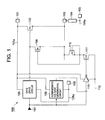
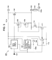
- Halbleiterausgangsschaltung, die folgendes umfasst:eine erste Stromversorgungsleitung (101a);einen Ausgangsanschluss (103) zur Verbindung mit einer zweiten Stromversorgungsleitung (105a) durch eine Last (104);einen Ausgangstransistor (102), der zwischen die ersten Stromversorgungsleitung und den Ausgangsanschluss gekoppelt ist und als Reaktion auf ein Steuersignal (107) angesteuert wird;einen Verarmungstyp-Transistor (108), der zwischen einen Steueranschluss des Ausgangstransistors und den Ausgangsanschluss gekoppelt ist;eine Zwischenspannungserzeugungsschaltung (150), die ein Zwischenpotenzial zwischen einem Potenzial der ersten Stromversorgungsleitung und einem Potenzial der zweiten Stromversorgungsleitung an einer Zwischenspannungsleitung (112) erzeugt;eine Reihenschaltung eines ersten Schalttransistors (111) und einer Impedanzvorrichtung (110), die zwischen die Zwischenspannungsleitung und den Ausgangsanschluss gekoppelt sind; undeinen Inverter (113), der mit einer Spannung zwischen dem Potenzial der ersten Stromversorgungsleitung und dem Zwischenpotenzial der Zwischenspannungsleitung betrieben wird und das Steuersignal invertiert, um ein invertiertes Steuersignal dem Gate des ersten Schalttransistors zuzuführen,wobeieine Spannung, die auf dem Zwischenpotenzial basiert, an ein Gate des Verarmungstyp-Transistors durch den ersten Schalttransistor angelegt wird, um den Verarmungstyp-Transistor auszuschalten, wenn der Ausgangstransistor sich in einem leitenden Zustand befindet; unddas Gate und eine Source des Verarmungstyp-Transistors miteinander durch die Impedanzvorrichtung elektrisch verbunden sind, um den Verarmungstyp-Transistor einzuschalten, wenn der Ausgangstransistor in einen nicht leitenden Zustand versetzt wird und der erste Schalttransistor sich in einem nicht leitenden Zustand befindet,gekennzeichnet durcheine Reihenschaltung eines zweiten Schalttransistors (114) und einer Konstantspannungsvorrichtung (115), die zwischen der ersten Stromversorgungsleitung und dem Ausgangsanschluss vorgesehen sind,wobeieine Ausgabe des Inverters dem Gate des zweiten Schalttransistors zugeführt wird; undein Knoten zwischen dem zweiten Schalttransistor und der Konstantspannungsvorrichtung mit der Source des Verarmungstyp-Transistors gekoppelt ist.
- Halbleiterausgangsschaltung gemäß Anspruch 1, die weiter eine Konstantstromquellenvorrichtung umfasst, die in Reihe mit dem Verarmungstyp-Transistor zwischen dem Steuerungsanschluss des Ausgangstransistors und dem Ausgangsanschluss vorgesehen ist.
- Halbleiterausgangsschaltung gemäß Anspruch 2, wobei die Konstantstromquellenvorrichtung einen Verarmungstyp-Transistor (109) umfasst.
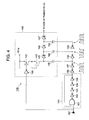
- Halbleiterausgangsschaltung gemäß Anspruch 1, wobei:der Ausgangstransistor durch eine Gate-Treiberschaltung (106) gesteuert wird undein Ausgang der Gate-Treiberschaltung einen Hochimpedanzzustand annimmt, wenn der Ausgangstransistor von dem leitenden Zustand in den nicht leitenden Zustand versetzt wird.
- Halbleiterausgangsschaltung gemäß Anspruch 4, wobei die Gate-Treiberschaltung als Reaktion auf ein Steuersignal, das den Ausgangstransistor in den leitenden Zustand versetzt, ein Potenzial erzeugt, das höher ist als das Potenzial der ersten Stromversorgungsleitung.
Applications Claiming Priority (2)
| Application Number | Priority Date | Filing Date | Title |
|---|---|---|---|
| JP2007329472 | 2007-12-21 | ||
| JP2008294518A JP5226474B2 (ja) | 2007-12-21 | 2008-11-18 | 半導体出力回路 |
Publications (3)
| Publication Number | Publication Date |
|---|---|
| EP2073385A2 EP2073385A2 (de) | 2009-06-24 |
| EP2073385A3 EP2073385A3 (de) | 2013-03-13 |
| EP2073385B1 true EP2073385B1 (de) | 2015-03-18 |
Family
ID=40513406
Family Applications (1)
| Application Number | Title | Priority Date | Filing Date |
|---|---|---|---|
| EP08021554.4A Active EP2073385B1 (de) | 2007-12-21 | 2008-12-11 | Halbleiterausgabeschaltung zur Steuerung der Stromversorgung an eine Last |
Country Status (2)
| Country | Link |
|---|---|
| US (1) | US7834669B2 (de) |
| EP (1) | EP2073385B1 (de) |
Families Citing this family (7)
| Publication number | Priority date | Publication date | Assignee | Title |
|---|---|---|---|---|
| JP2010193033A (ja) * | 2009-02-17 | 2010-09-02 | Renesas Electronics Corp | 過電流保護回路 |
| JP5341781B2 (ja) * | 2010-01-04 | 2013-11-13 | ルネサスエレクトロニクス株式会社 | 電力供給制御回路 |
| JP5341780B2 (ja) * | 2010-01-04 | 2013-11-13 | ルネサスエレクトロニクス株式会社 | 電力供給制御回路 |
| JP5889723B2 (ja) | 2012-06-07 | 2016-03-22 | ルネサスエレクトロニクス株式会社 | 半導体装置 |
| US9755638B2 (en) * | 2014-11-12 | 2017-09-05 | Texas Instruments Incorporated | Output discharge techniques for load switches |
| US9917578B2 (en) | 2016-02-19 | 2018-03-13 | Infineon Technologies Austria Ag | Active gate-source capacitance clamp for normally-off HEMT |
| JP6871514B2 (ja) * | 2017-06-30 | 2021-05-12 | ミツミ電機株式会社 | 負電源制御回路及び電源装置 |
Family Cites Families (9)
| Publication number | Priority date | Publication date | Assignee | Title |
|---|---|---|---|---|
| US5055722A (en) * | 1989-12-20 | 1991-10-08 | Sundstrand Corporation | Gate drive for insulated gate device |
| JP2646786B2 (ja) | 1990-02-27 | 1997-08-27 | 日本電気株式会社 | 半導体出力回路 |
| EP0489935B1 (de) * | 1990-11-09 | 1995-11-02 | Siemens Aktiengesellschaft | MOSFET-Schalter für eine induktive Last |
| US5272399A (en) * | 1992-02-25 | 1993-12-21 | Siemens Aktiengesellschaft | Circuit limiting the load current of a power MOSFET |
| DE59207678D1 (de) * | 1992-06-05 | 1997-01-23 | Siemens Ag | Ansteuerschaltung für einen Leistungs-FET mit sourceseitiger Last |
| US5910738A (en) * | 1995-04-07 | 1999-06-08 | Kabushiki Kaisha Toshiba | Driving circuit for driving a semiconductor device at high speed and method of operating the same |
| DE19631751C1 (de) * | 1996-08-06 | 1997-11-27 | Siemens Ag | Ansteuerschaltung für einen Leistungs-FET mit sourceseitiger Last |
| DE10033440C2 (de) * | 2000-07-10 | 2002-07-18 | Infineon Technologies Ag | Ansteuerschaltung für einen Leistungs-MOSFET |
| DE10038220C2 (de) * | 2000-08-04 | 2002-07-25 | Infineon Technologies Ag | Überstromgeschützter Halbleiterleistungsschalter mit Ladungspumpe |
-
2008
- 2008-12-10 US US12/314,420 patent/US7834669B2/en active Active
- 2008-12-11 EP EP08021554.4A patent/EP2073385B1/de active Active
Also Published As
| Publication number | Publication date |
|---|---|
| US20090160498A1 (en) | 2009-06-25 |
| EP2073385A3 (de) | 2013-03-13 |
| EP2073385A2 (de) | 2009-06-24 |
| US7834669B2 (en) | 2010-11-16 |
Similar Documents
| Publication | Publication Date | Title |
|---|---|---|
| US8040162B2 (en) | Switch matrix drive circuit for a power element | |
| US8547142B2 (en) | Power semiconductor device and operation method thereof | |
| EP2073385B1 (de) | Halbleiterausgabeschaltung zur Steuerung der Stromversorgung an eine Last | |
| US7606015B2 (en) | Power semiconductor device architecture for output transistor protection | |
| EP2315354B1 (de) | Halbleiterbauelement | |
| US9973082B1 (en) | Load driving circuit | |
| US10840898B2 (en) | Semiconductor device and electronic control device | |
| EP2073386B1 (de) | Halbleiterausgabeschaltung | |
| US11711010B2 (en) | Drive circuit and inverter device | |
| US20110057633A1 (en) | Load driving circuit | |
| US20030155958A1 (en) | Drive circuit | |
| US6856177B1 (en) | High side power switch with charge pump and bootstrap capacitor | |
| CN111917403A (zh) | 用于降低死区时间效率低下的栅极驱动器电路 | |
| JP4658770B2 (ja) | 半導体装置 | |
| US11070202B2 (en) | Signal transmission circuit, switch driving device, and power module | |
| CN114204926A (zh) | 半导体装置 | |
| JP5226474B2 (ja) | 半導体出力回路 | |
| CN112640279B (zh) | 过电流保护电路及开关电路 | |
| JP2009171552A (ja) | 半導体出力回路 | |
| JP3824602B2 (ja) | スイッチング制御装置及びスイッチング制御方法 | |
| JP2022006505A (ja) | チャージポンプ装置 |
Legal Events
| Date | Code | Title | Description |
|---|---|---|---|
| PUAI | Public reference made under article 153(3) epc to a published international application that has entered the european phase |
Free format text: ORIGINAL CODE: 0009012 |
|
| AK | Designated contracting states |
Kind code of ref document: A2 Designated state(s): AT BE BG CH CY CZ DE DK EE ES FI FR GB GR HR HU IE IS IT LI LT LU LV MC MT NL NO PL PT RO SE SI SK TR |
|
| AX | Request for extension of the european patent |
Extension state: AL BA MK RS |
|
| RAP1 | Party data changed (applicant data changed or rights of an application transferred) |
Owner name: RENESAS ELECTRONICS CORPORATION |
|
| REG | Reference to a national code |
Ref country code: DE Ref legal event code: R079 Ref document number: 602008037167 Country of ref document: DE Free format text: PREVIOUS MAIN CLASS: H03K0017080000 Ipc: H03K0017060000 |
|
| PUAL | Search report despatched |
Free format text: ORIGINAL CODE: 0009013 |
|
| AK | Designated contracting states |
Kind code of ref document: A3 Designated state(s): AT BE BG CH CY CZ DE DK EE ES FI FR GB GR HR HU IE IS IT LI LT LU LV MC MT NL NO PL PT RO SE SI SK TR |
|
| AX | Request for extension of the european patent |
Extension state: AL BA MK RS |
|
| RIC1 | Information provided on ipc code assigned before grant |
Ipc: H03K 17/06 20060101AFI20130207BHEP Ipc: H03K 17/16 20060101ALI20130207BHEP |
|
| 17P | Request for examination filed |
Effective date: 20130725 |
|
| RBV | Designated contracting states (corrected) |
Designated state(s): AT BE BG CH CY CZ DE DK EE ES FI FR GB GR HR HU IE IS IT LI LT LU LV MC MT NL NO PL PT RO SE SI SK TR |
|
| 17Q | First examination report despatched |
Effective date: 20130906 |
|
| AKX | Designation fees paid |
Designated state(s): DE |
|
| GRAP | Despatch of communication of intention to grant a patent |
Free format text: ORIGINAL CODE: EPIDOSNIGR1 |
|
| GRAJ | Information related to disapproval of communication of intention to grant by the applicant or resumption of examination proceedings by the epo deleted |
Free format text: ORIGINAL CODE: EPIDOSDIGR1 |
|
| GRAP | Despatch of communication of intention to grant a patent |
Free format text: ORIGINAL CODE: EPIDOSNIGR1 |
|
| INTG | Intention to grant announced |
Effective date: 20140924 |
|
| RAP1 | Party data changed (applicant data changed or rights of an application transferred) |
Owner name: RENESAS ELECTRONICS CORPORATION |
|
| INTG | Intention to grant announced |
Effective date: 20141007 |
|
| GRAS | Grant fee paid |
Free format text: ORIGINAL CODE: EPIDOSNIGR3 |
|
| GRAA | (expected) grant |
Free format text: ORIGINAL CODE: 0009210 |
|
| AK | Designated contracting states |
Kind code of ref document: B1 Designated state(s): DE |
|
| REG | Reference to a national code |
Ref country code: DE Ref legal event code: R096 Ref document number: 602008037167 Country of ref document: DE Effective date: 20150430 |
|
| REG | Reference to a national code |
Ref country code: DE Ref legal event code: R097 Ref document number: 602008037167 Country of ref document: DE |
|
| PLBE | No opposition filed within time limit |
Free format text: ORIGINAL CODE: 0009261 |
|
| STAA | Information on the status of an ep patent application or granted ep patent |
Free format text: STATUS: NO OPPOSITION FILED WITHIN TIME LIMIT |
|
| 26N | No opposition filed |
Effective date: 20151221 |
|
| REG | Reference to a national code |
Ref country code: DE Ref legal event code: R082 Ref document number: 602008037167 Country of ref document: DE Representative=s name: GLAWE DELFS MOLL PARTNERSCHAFT MBB VON PATENT-, DE Ref country code: DE Ref legal event code: R081 Ref document number: 602008037167 Country of ref document: DE Owner name: RENESAS ELECTRONICS CORPORATION, JP Free format text: FORMER OWNER: RENESAS ELECTRONICS CORP., KAWASAKI-SHI, KANAGAWA, JP |
|
| REG | Reference to a national code |
Ref country code: DE Ref legal event code: R082 Ref document number: 602008037167 Country of ref document: DE Representative=s name: GLAWE DELFS MOLL PARTNERSCHAFT MBB VON PATENT-, DE |
|
| PGFP | Annual fee paid to national office [announced via postgrant information from national office to epo] |
Ref country code: DE Payment date: 20231227 Year of fee payment: 16 |