EP2070601B1 - Low dielectric constant plasma polymerized thin film and manufacturing method thereof - Google Patents
Low dielectric constant plasma polymerized thin film and manufacturing method thereof Download PDFInfo
- Publication number
- EP2070601B1 EP2070601B1 EP08170636A EP08170636A EP2070601B1 EP 2070601 B1 EP2070601 B1 EP 2070601B1 EP 08170636 A EP08170636 A EP 08170636A EP 08170636 A EP08170636 A EP 08170636A EP 2070601 B1 EP2070601 B1 EP 2070601B1
- Authority
- EP
- European Patent Office
- Prior art keywords
- thin film
- plasma
- set forth
- annealing
- substrate
- Prior art date
- Legal status (The legal status is an assumption and is not a legal conclusion. Google has not performed a legal analysis and makes no representation as to the accuracy of the status listed.)
- Active
Links
Images


Classifications
-
- B—PERFORMING OPERATIONS; TRANSPORTING
- B05—SPRAYING OR ATOMISING IN GENERAL; APPLYING FLUENT MATERIALS TO SURFACES, IN GENERAL
- B05D—PROCESSES FOR APPLYING FLUENT MATERIALS TO SURFACES, IN GENERAL
- B05D1/00—Processes for applying liquids or other fluent materials
- B05D1/62—Plasma-deposition of organic layers
-
- C—CHEMISTRY; METALLURGY
- C08—ORGANIC MACROMOLECULAR COMPOUNDS; THEIR PREPARATION OR CHEMICAL WORKING-UP; COMPOSITIONS BASED THEREON
- C08J—WORKING-UP; GENERAL PROCESSES OF COMPOUNDING; AFTER-TREATMENT NOT COVERED BY SUBCLASSES C08B, C08C, C08F, C08G or C08H
- C08J5/00—Manufacture of articles or shaped materials containing macromolecular substances
- C08J5/20—Manufacture of shaped structures of ion-exchange resins
- C08J5/22—Films, membranes or diaphragms
- C08J5/2206—Films, membranes or diaphragms based on organic and/or inorganic macromolecular compounds
- C08J5/2218—Synthetic macromolecular compounds
- C08J5/2256—Synthetic macromolecular compounds based on macromolecular compounds obtained by reactions other than those involving carbon-to-carbon bonds, e.g. obtained by polycondensation
-
- C—CHEMISTRY; METALLURGY
- C08—ORGANIC MACROMOLECULAR COMPOUNDS; THEIR PREPARATION OR CHEMICAL WORKING-UP; COMPOSITIONS BASED THEREON
- C08J—WORKING-UP; GENERAL PROCESSES OF COMPOUNDING; AFTER-TREATMENT NOT COVERED BY SUBCLASSES C08B, C08C, C08F, C08G or C08H
- C08J5/00—Manufacture of articles or shaped materials containing macromolecular substances
- C08J5/20—Manufacture of shaped structures of ion-exchange resins
- C08J5/22—Films, membranes or diaphragms
- C08J5/2287—After-treatment
-
- C—CHEMISTRY; METALLURGY
- C08—ORGANIC MACROMOLECULAR COMPOUNDS; THEIR PREPARATION OR CHEMICAL WORKING-UP; COMPOSITIONS BASED THEREON
- C08K—Use of inorganic or non-macromolecular organic substances as compounding ingredients
- C08K5/00—Use of organic ingredients
- C08K5/01—Hydrocarbons
-
- C—CHEMISTRY; METALLURGY
- C08—ORGANIC MACROMOLECULAR COMPOUNDS; THEIR PREPARATION OR CHEMICAL WORKING-UP; COMPOSITIONS BASED THEREON
- C08K—Use of inorganic or non-macromolecular organic substances as compounding ingredients
- C08K5/00—Use of organic ingredients
- C08K5/54—Silicon-containing compounds
-
- H—ELECTRICITY
- H01—ELECTRIC ELEMENTS
- H01L—SEMICONDUCTOR DEVICES NOT COVERED BY CLASS H10
- H01L21/00—Processes or apparatus adapted for the manufacture or treatment of semiconductor or solid state devices or of parts thereof
- H01L21/02—Manufacture or treatment of semiconductor devices or of parts thereof
- H01L21/04—Manufacture or treatment of semiconductor devices or of parts thereof the devices having at least one potential-jump barrier or surface barrier, e.g. PN junction, depletion layer or carrier concentration layer
- H01L21/18—Manufacture or treatment of semiconductor devices or of parts thereof the devices having at least one potential-jump barrier or surface barrier, e.g. PN junction, depletion layer or carrier concentration layer the devices having semiconductor bodies comprising elements of Group IV of the Periodic System or AIIIBV compounds with or without impurities, e.g. doping materials
- H01L21/20—Deposition of semiconductor materials on a substrate, e.g. epitaxial growth solid phase epitaxy
-
- B—PERFORMING OPERATIONS; TRANSPORTING
- B05—SPRAYING OR ATOMISING IN GENERAL; APPLYING FLUENT MATERIALS TO SURFACES, IN GENERAL
- B05D—PROCESSES FOR APPLYING FLUENT MATERIALS TO SURFACES, IN GENERAL
- B05D3/00—Pretreatment of surfaces to which liquids or other fluent materials are to be applied; After-treatment of applied coatings, e.g. intermediate treating of an applied coating preparatory to subsequent applications of liquids or other fluent materials
- B05D3/02—Pretreatment of surfaces to which liquids or other fluent materials are to be applied; After-treatment of applied coatings, e.g. intermediate treating of an applied coating preparatory to subsequent applications of liquids or other fluent materials by baking
- B05D3/0254—After-treatment
Definitions
- the present invention relates in general to a low dielectric constant plasma polymerized thin film and a manufacturing method thereof, and more particularly, to a plasma polymerized thin film for use in semiconductor devices, which has a low dielectric constant and shows improved insulating property and is also improved in terms of mechanical properties including hardness and elastic modulus, and to a method of manufacturing the same.
- CVD chemical vapor deposition
- reactant gases are supplied to the surface of a substrate, so that a thermally-induced chemical reaction occurs on the surface of the substrate, thus forming a thin film of a predetermined thickness.
- thermal CVD process is conducted at high temperatures, which may thus damage device geometries in which layers are formed on the substrate.
- a preferred example of a method of depositing metal and dielectric thin films at relatively low temperatures includes plasma-enhanced CVD (PECVD) disclosed in US Patent No. 5,362,526 , entitled “Plasma-enhanced CVD process using TEOS for depositing silicon oxide", which is hereby incorporated by reference into this application.
- WO2004/083495 discloses a method for forming a multiphase, low dielectric constant plasma polymerized thin film.
- radio frequency (RF) energy is applied to a reaction zone, thus promoting the excitation and/or dissociation of reactant gases, thereby creating plasma of highly reactive species.
- High reactivity of the released species reduces the energy required for a chemical reaction to take place and thus lowers the required temperature for such PECVD.
- semiconductor device geometries have dramatically decreased in size due to the introduction of such an apparatus and method.
- Such a low dielectric constant thin film is formed of an organic material or an inorganic material such as a fluorine (F)-doped oxide film (SiO 2 ) and a fluorine-doped amorphous carbon film (a-C:F).
- F fluorine
- SiO 2 fluorine-doped oxide film
- a-C:F fluorine-doped amorphous carbon film
- Examples of the low dielectric constant material presently usable instead of SiO 2 include organic polymers for spin coating, such as BCB (benzocyclobutene), SILK (available from DOW Chemical), FLARE (fluorinated poly(arylene ether), available from Allied Signals), and polyimide, materials for CVD, such as Black Diamond (available from Applied Materials), Coral (available from Novellus), SiOF, alkyl silane, and parylene, and porous thin film materials, such as xerogel or aerogel.
- organic polymers for spin coating such as BCB (benzocyclobutene), SILK (available from DOW Chemical), FLARE (fluorinated poly(arylene ether), available from Allied Signals), and polyimide
- materials for CVD such as Black Diamond (available from Applied Materials), Coral (available from Novellus), SiOF, alkyl silane, and parylene, and porous thin film materials, such as xerogel or aerogel.
- the low dielectric constant thin film thus formed advantageously has a low dielectric constant because the pores having a size of single-digits of nanometers are formed in the thin film, thus lowering the density of the thin film.
- the organic polymers which are typically deposited through spin coating have a low dielectric constant and superior planarization, but have poor thermal stability due to low heat-resistant threshold temperatures below 450°C and are thus inadequate in terms of availability. Further, the above organic polymers are disadvantageous because the pores are non-uniformly distributed in the film owing to a large size thereof, thus causing many problems upon the manufacture of devices.
- the above organic polymers are problematic in that they come into poor contact with upper and lower wiring materials, that thin films resulting therefrom intrinsically incur high stress upon thermal curing, and also that the dielectric constant thereof varies attributable to water absorption, undesirably decreasing the reliability of the device.
- the present invention provides a low dielectric constant plasma polymerized thin film which is improved in terms of dielectric constant, mechanical properties and the insulating property and also provides a method of manufacturing the same.
- a low dielectric constant plasma polymerized thin film may be manufactured using precursors represented by Formulas 1 and 2 below.
- R 1 to R 6 are each independently selected from the group consisting of a hydrogen atom and substituted or unsubstituted C 1-5 alkyl groups, and X is an oxygen atom or a C 1-5 alkylene group.
- R 1 to R 5 are each independently selected from the group consisting of a hydrogen atom; and substituted or unsubstituted C 1-5 alkyl groups
- R 6 is selected from the group consisting of a hydrogen atom; and substituted or unsubstituted C 1-5 alkyl groups and alkoxysilane groups.
- R 6 of Formula 2 may represent -O-Si(R 7 ) 3 ; and wherein R 7 may be selected from the group consisting of C 1-6 alkyl groups and phenyl groups.
- the low dielectric constant polymerized thin film may be manufactured using PECVD.
- the precursor represented by Formula 1 may be hexamethyldisiloxane, and the precursor represented by Formula 2 may be 3,3-dimethyl-1-butene or allyloxytrimethylsilane.
- a method of manufacturing a low dielectric constant plasma polymerized thin film may comprise depositing a plasma polymerized thin film on a substrate using precursors represented by Formulas 1 and 2 below through PECVD, and annealing the deposited thin film using an RTA apparatus.
- R 1 to R 6 are each independently selected from the group consisting of a hydrogen atom and substituted or unsubstituted C 1-5 alkyl groups, and X is an oxygen atom or a C 1-5 alkylene group.
- R 1 to R 5 are each independently selected from the group consisting of a hydrogen atom; and substituted or unsubstituted C 1-5 alkyl groups
- R 6 is selected from the group consisting of a hydrogen atom; and substituted or unsubstituted C 1-5 alkyl groups and alkoxysilane groups.
- R 6 of Formula 2 may represent -O-Si(R 7 ) 3 ; and wherein R 7 may be selected from the group consisting of C 1-6 alkyl groups and phenyl groups.
- the precursor represented by Formula 1 may be hexamethyldisiloxane, and the precursor represented by Formula 2 may be 3,3-dimethyl-1-butene or allyloxytrimethylsilane.
- depositing the plasma polymerized thin film on the substrate may comprise vaporizing the precursors represented by Formulas 1 and 2 in bubblers, supplying the gaseous precursors into a reactor for plasma deposition from the bubblers, and forming a plasma polymerized thin film on the substrate in the reactor using plasma of the reactor.
- the supplying the gaseous precursors into a reactor for plasma deposition from the bubblers may include a carrier gas of the reactor, and the carrier gas is argon(Ar) or helium(He); and wherein a pressure of the carrier gas is 1 ⁇ 10 -1 ⁇ 100 ⁇ 10 -1 Torr. Also, the temperature of the substrate may be 20 ⁇ 50°C, and power supplied to the reactor may be 15 ⁇ 80 W.
- the method further may include an annealing treatment or a plasma treatment on the plasma polymerized thin film after the forming a plasma polymerized thin film on the substrate in the reactor.
- the carrier gas of the reactor as a plasma gas, in the additional plasma treatment, may be selected from the group consisting of argon(Ar), helium (He) and a mixture gas of hydrogen and helium; and a pressure of the carrier gas may be 1 ⁇ 10 -3 ⁇ 1 ⁇ 10 -1 Torr.
- the mixture gas of hydrogen and helium may consist of about 5 to 15 volume% of hydrogen gas and about 95 to 85 volume% of helium gas.
- annealing the deposited thin film using the RTA apparatus may be conducted by placing the substrate having the plasma polymerized thin film deposited thereon in a chamber of the RTA apparatus, and generating heat on the substrate using a plurality of halogen lamps disposed around the chamber.
- annealing the deposited thin film using the RTA apparatus may be conducted in nitrogen gas. Tn the method according to the present invention, annealing the deposited thin film using the RTA apparatus may be conducted by increasing the temperature of the substrate to 300 ⁇ 600°C and then performing annealing, and preferably by increasing the temperature of the substrate to 300 ⁇ 600°C within 5 min and then performing annealing for 1 - 5 min.
- annealing the deposited thin film using the RTA apparatus may be conducted at a pressure of 0.5 - 1.5 Torr.
- a low dielectric constant plasma polymerized thin film is manufactured using precursors represented by Formulas 1 and 2 below.
- R 1 to R 6 are each independently selected from the group consisting of a hydrogen atom and substituted or unsubstituted C 1-5 alkyl groups, and X is an oxygen atom or a C 1-5 alkylene group.
- R 1 to R 5 are each independently selected from the group consisting of a hydrogen atom; and substituted or unsubstituted C 1-5 alkyl groups
- R 6 is selected from the group consisting of a hydrogen atom; and substituted or unsubstituted C 1-5 alkyl groups and alkoxysilane groups.
- the alkyl group has 1 ⁇ 5 carbon atoms and examples thereof include a methyl group, an ethyl group, a propyl group, and a butyl group.
- the alkyl group may be linear or branched, and one or more hydrogen atoms thereof may be substituted with a substituent such as a fluorine atom.
- X which is a linker may be an oxygen atom (-O-) or a C 1-5 alkylene group such as a methylene group or an ethylene group. Particularly useful is an oxygen atom (-O-).'
- the alkyl group has 1 ⁇ 5 carbon atoms and examples thereof include a methyl group, an ethyl group, a propyl group, and a butyl group, as in Formula 1.
- the alkyl group may be linear or branched, and one or more hydrogen atoms thereof may be substituted with a substituent such as a fluorine atom.
- R 6 of Formula 2 is alkoxysilane groups
- R 6 may represent -O-Si(R 7 ) 3
- R 7 may be selected from the group consisting of C 1 ⁇ 6 alkyl groups and phenyl groups.
- R 1 to R 3 be a hydrogen atom.
- an example of the precursor represented by Formula 1 includes hexamethyldisiloxane represented by Formula 3 below. Also, it can be considered as one of examples that the precursor of Formula 2 is formed to include, 3-dimethyl-1-butene (neohexene) represented by Formula 4 below or allyloxytrimethylsilane by Formula 5 below.
- the linear organic/inorganic precursors of Formulas 1 and 2 may be used in combinations thereof, such that pores having a size of nanometers or smaller are formed in the polymerized thin film. Further, the dielectric constant is remarkably decreased, and as well, mechanical properties including hardness and elastic modulus may be increased.
- the low dielectric constant plasma polymerized thin film is preferably manufactured using PECVD, in order to reduce the complicated process and long process time for pretreatment and post-treatment arising in a spin casting process.
- the present invention provides a method of manufacturing the low dielectric constant plasma polymerized thin film using PECVD, including depositing a plasma polymerized thin film on a substrate using the precursors of Formulas 1 and 2 and annealing the deposited thin film using an RTA apparatus.
- depositing the plasma polymerized thin film on the substrate includes vaporizing the precursors of Formulas 1 and 2 in bubblers, supplying the gaseous precursors into a reactor for plasma deposition from the bubblers, and forming a plasma polymerized thin film on a substrate in the reactor using plasma of the reactor.
- a carrier gas of the reactor may use argon(Ar) or helium(He); and a pressure of the carrier gas may be 1 ⁇ 10 -1 ⁇ 100 ⁇ 10 -1 Torr. If the pressure of the carrier gas falls outside of the above range, the deposition rate may be lowered.
- the method further may include an annealing treatment or a plasma treatment on the plasma polymerized thin film after the forming a plasma polymerized thin film on the substrate in the reactor. Additional process of the annealing treatment or the plasma treatment may make improvements to the properties of the thin film.
- the annealing treatment may be conducted that the plasma polymerized thin film is annealed to 300 - 600°C, for 30 min to 4hr.
- the plasma treatment may be conducted that the substrate coated with the plasma polymerized thin film is loaded in the reactor followed by the plasma treatment using the carrier gas at appropriate pressure.
- a plasma gas that is a carrier gas of the reactor may be selected from the group consisting of argon(Ar), helium(He) and a mixture gas of hydrogen and helium.
- the pressure of the carrier gas may be 1 ⁇ 10 -3 ⁇ 1 ⁇ 10 -1 Torr. If the pressure of the carrier gas falls outside of the above range, the insulating property of the thin film may be deteriorated.
- the mixture gas of hydrogen and helium may consist of about 5 to 15 volume% of hydrogen gas and about 95 to 85 volume% of helium gas. If the volume of hydrogen is less then than 5 volume%, there may be an effect caused by He gas, but there may be little effect caused by added hydrogen gas. On the other hand, if the volume of hydrogen exceeds 15 volume%, there may be modification in the structure of the thin film.
- a PECVD apparatus for performing the PECVD process includes a reactor which is a process chamber composed of an upper chamber lid and a lower chamber body, for performing the thin film deposition process.
- the reactant gases are uniformly sprayed onto a substrate placed on the upper surface of a susceptor formed in the chamber body via shower heads provided in the chamber lid, thus depositing the thin film.
- This reaction is activated by RF energy which is supplied through an electrode mounted in the susceptor, such that the thin film deposition process is carried out.
- the thin film thus deposited is placed on the susceptor of the RTA apparatus as an annealing apparatus, after which the annealing process is rapidly conducted at predetermined temperatures.
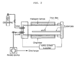
- FIG. 1 shows the PECVD apparatus used for manufacturing the low dielectric constant plasma polymerized thin film according to the present invention.
- PECVD apparatus includes, but is not limited to, an electric condenser type PECVD apparatus. Alternatively, other kinds of PECVD apparatus may be used.
- the PECVD apparatus includes first and second carrier gas storing portions 10, 11 containing a carrier gas such as Ar, first and second flow rate controllers 20, 21 for controlling the number of moles of gases passing therethrough, first and second bubblers 30, 31 containing solid or liquid precursors, a reactor 50 in which the reaction occurs, and a RF generator 40 for generating plasma in the reactor 50.
- the carrier gas storing portions 10, 11, the flow rate controllers 20, 21, the bubblers 30, 31, and the reactor 50 are connected through a pipeline 60.
- a susceptor 51 connected to the RF generator 40 for generating plasma and for supporting the substrate 1 thereon is provided.
- a heater (not shown) is embedded in the susceptor 51, so that the substrate 1 placed on the susceptor 51 is heated to a temperature appropriate for deposition in the course of thin film deposition.
- an exhaust system is provided under the reactor 50 so as to discharge the reactant gases remaining in the reactor 50 after the completion of the deposition reaction.
- the method of depositing the thin film using the PECVD apparatus is described below.
- a substrate 1 made of silicon (P ++ -Si) doped with boron having metallic properties is washed with trichloroethylene, acetone, or methanol, and is then placed on the susceptor 51 of the reactor 50.
- the first and second bubblers 30, 31 respectively contain precursors of Formulas 1 and 2, and the first and second bubblers 30, 31 are heated to temperatures adequate for the vaporization of the respective precursors.
- the two types of precursors be respectively loaded into the two bubblers 30, 31, without discrimination of the bubblers, and the heating temperature of the bubblers be controlled depending on the types of precursors respectively loaded therein.
- a carrier gas selected from among argon (Ar) or helium (He) is loaded and flows via the pipeline 60 by means of the first and second flow rate controllers 20, 21.
- the carrier gas flowing along the pipeline 60 is introduced into the precursor solutions of the bubblers 30, 31 via the inlet ports of the bubblers so that bubbles occur, after which it flows along with the gaseous precursors again into the pipeline 60 passing out via the outlet ports of the bubblers.
- the carrier gas and the gaseous precursors flowing along the pipeline 60 from the bubblers 30, 31 are sprayed through the shower heads 53 of the reactor 50.
- the RF generator 40 is connected to the shower heads 53 so that the reactant gases sprayed through the shower heads 53 are converted into a plasma state.
- the precursors, which are sprayed through the shower heads 53 of the reactor 50 and converted into a plasma state, are deposited on the substrate 1 placed on the susceptor 51, thus forming a thin film.
- the gases remaining after the completion of the deposition reaction are discharged to the outside via the exhaust system provided under the reactor.
- the pressure of the carrier gas of the reactor 50 is set to 1 ⁇ 10 -1 ⁇ 100 ⁇ 10 -1 Torr to optimize the formation of the thin film, and the temperature of the substrate 1 is preferably 20 - 50°C. If the temperature of the substrate 1 falls outside of the above range, the deposition rate is lowered.
- the temperature of the substrate 1 is controlled using a heater embedded in the susceptor. Further, power supplied to the RF generator 40 may be 15 - 80 W. In the case where the magnitude of power is above or below the above range, the formation of the low dielectric constant thin film is hard to achieve.
- the frequency of plasma thus generated is 10 - 20 MHz.
- the pressure of the carrier gas, the temperature of the substrate 1, and the supplying power are set to form the optimal plasma frequency so that the precursors are converted into a plasma state and then deposited on the substrate 1, and may be appropriately adjusted depending on the types of precursors.
- the above factors are adjusted so that the plasma frequency is about 13.56 MHz.
- an annealing treatment or a plasma treatment may be added.
- FIG. 2 shows the RTA (rapid thermal annealing) apparatus for performing the annealing process.
- the RTA apparatus is used to perform the heat treatment of a specimen, activate electrons in a semiconductor device process, change the properties of an interface between a thin film and a thin film or between a wafer and a thin film, and increase the density of a thin film. Further, this apparatus functions to convert the state of the grown thin film, decrease the loss due to ion implantation, and aid the transport of electrons from a thin film to another thin film or from a thin film to a wafer.
- Such RTA is carried out using heated halogen lamps and hot chucks.
- the RTA process may be conducted for a process time shorter than when using a furnace, and is thus referred to as RTP (Rapid Thermal Process). Using such a heat treatment apparatus, the plasma deposited thin film is annealed.
- the substrate 1 having the thin film deposited thereon is placed in a chamber of the RTA apparatus, and heat is generated while orange light is emitted, using a plurality of halogen lamps (wavelength: about 2 ⁇ m) disposed around the chamber.
- the RTA process is preferably performed by annealing the substrate having the plasma deposited thin film placed thereon at 300 ⁇ 600°C. If the annealing temperature is lower than 300°C, the properties of the initially deposited thin film are not changed. Conversely, if the annealing temperature is higher than 600°C, the structure of the thin film may be undesirably converted from the low dielectric constant thin film into an SiO 2 thin film.
- the treatment temperature is increased to the above annealing temperature within 5 min and then annealing is performed for 1 - 5 min in order to effectively change the structure of the thin film.
- the RTA is performed at a pressure of 1 ⁇ 10 -1 ⁇ 100 ⁇ 10 -1 Torr in nitrogen gas.
- precursors for example, hexamethyldisiloxane (hereinafter referred to as 'HMDSO') and 3,3-dimethyl-1-butene (hereinafter referred to as 'DMB') were respectively loaded into first and second bubblers 30, 31, after which the bubblers were respectively heated to 55°C and 45°C, thus vaporizing the precursor solutions.
- the gaseous precursors were sprayed along with argon (Ar) gas, having an ultra high purity of 99.999% and acting as a carrier gas, through the shower heads 53 of a reactor 50 for plasma deposition, and were then plasma-deposited on the substrate 1.
- the pressure of Ar of the reactor 50 was 5 ⁇ 10 -1 Torr, and the temperature of the substrate was 35°C.
- power supplied to the RF generator was 15 - 80W, and the resulting plasma frequency was about 13.56 MHz.
- the plasma polymerized thin film thus deposited is referred to as 'HMDSO: DMB'.
- the thickness of the HMDSO: DMB was measured to be 0.4 - 0.5 ⁇ m.
- the deposition is supposed to occur according to the following mechanism. Specifically, monomers of the precursor mixture transferred into the reactor 50 are activated or decomposed to reactive species by means of plasma and thus condensed on the substrate 1. As such, because the cross-linking between the molecules of HMDSO and DMB is easily formed, the HMDSO:DMB deposited under appropriate conditions is easily crosslinked due to the silicon oxide group and the methyl group of HMDSO and thus has good thermal stability, and also, the polymerization between the methyl group of HMDSO and DMB is seen to efficiently take place.
- the HMDSO:DMB thus obtained was annealed using an RTA apparatus illustrated in FIG. 2 .
- the HMDSO:DMB was placed on a substrate 1, and heat was generated by means of 12 halogen lamps (wavelength: about 2 ⁇ m) disposed around the substrate, so that the HMDSO:DMB was annealed to 450°C for 5 min in a nitrogen atmosphere.
- the pressure of nitrogen gas was 1.0 Torr.
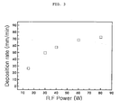
- FIG. 3 is a graph showing the deposition rate of the HMDSO: DMB. The deposition rate was seen to be increased in proportion to the increase in power.
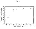
- FIG. 4 is a graph showing the thermal stability of the annealed HMDSO: DMB. After performing the annealing process at 450°C for 5 min, the thin film was maintained to the extent of 95% or more. Therefore, the low dielectric constant plasma polymerized thin film according to the present invention could be confirmed to have excellent thermal stability.
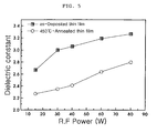
- FIG. 5 is a graph showing the relative dielectric constant for the HMDSO: DMB and the annealed HMDSO: DMB.
- the dielectric constant was measured by applying signals of frequency of 1 MHz to an electric condenser having a structure of Al/HMDSO: DMB /metallic-Si provided on a silicon substrate having very low resistance. As the power was increased, the dielectric constant of the HMDSO: DMB was measured. In this case, the relative dielectric constant of the HMDSO: DMB was increased from 2.67 to 3.27, and the relative dielectric constant of the annealed HMDSO: DMB was increased from 2.27 to 2.8. Thereby, the relative dielectric constant of the RTA-treated thin film was seen to be much lower than the dielectric constant of the plasma deposited thin film.
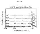
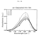
- FIGS. 6A and 6B are graphs showing the chemical structures of the HMDSO: DMB and the annealed HMDSO: DMB, respectively, obtained through Fourier transform infrared spectroscopy.
- the initial HMDSO: DMB and the annealed HMDSO: DMB stretching vibrations for the respective chemical structures were generated at the same positions over the entire wavenumber range.
- the HMDSO: DMB and the annealed HMDSO: DMB were confirmed to have similar bonding structures.
- FIGS. 7A and 7B are graphs showing the chemical structures of hydrocarbon-based bonds of the HMDSO: DMB and the annealed HMDSO: DMB, respectively, obtained through Fourier transform infrared spectroscopy.
- FIGS. 8A and 8B are graphs showing the chemical structures of silicon-oxygen-based bonds of the HMDSO: DMB and the annealed HMDSO: DMB, respectively, obtained through Fourier transform infrared spectroscopy.
- FIG. 9 is a graph showing the hardness of the HMDSO: DMB and the annealed HMDSO: DMB, as measured using a nano-indentor.
- the hardness of the HMDSO: DMB was increased from 0.13 GPa to 2.50 GPa
- the hardness of the annealed HMDSO: DMB was increased from 0.05 GPa to 2.66 GPa.
- FIG. 10 is a graph showing the elastic modulus of the HMDSO: DMB and the annealed HMDSO: DMB.
- the elastic modulus of the HMDSO: DMB was increased from 2.25 GPa to 21.81 GPa
- the elastic modulus of the annealed HMDSO: DMB was increased from 1.66 GPa to 18.9 GPa; the elastic modulus of the annealed thin film was lower than that of the plasma-deposited thin film.
- Example 2 was conducted in the same manner as in Example 1 except that the HMDSO and allyloxytrimethylsilane (hereinafter referred to as 'AOTMS') were used as precursors and the HMDSO and the AOTMS were respectively loaded into first and second bubblers, after which the bubblers were respectively heated to 45°C and 80°C.
- the plasma polymerized thin film thus deposited is referred to as 'HMDSO: AOTMS'.
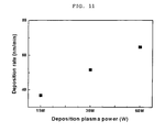
- FIG.11 is a graph showing the deposition rate of the HMDSO:AOTMS in accordance with the deposition plasma power. It is noted that the deposition rate was increased from 36 nm/min to 64 nm/min in proportion to the increase in power from 15W to 60W.
- FIG.11 is a graph showing the deposition rate of the HMDSO:AOTMS in accordance with the deposition plasma power. It is noted that the deposition rate was increased from 36 nm/min to 64 nm/min in proportion to the increase in power from 15W to 60W
- FIG. 12 is a graph showing the dielectric constant of the HMDSO:AOTMS in accordance with the deposition plasma power of the thin film. It is noted that the dielectric constant of the HMDSO: AOTMS was increased from 2.6 to 3.4 when the deposition plasma power was increased from 15W to 60W.
- a plasma treatment was carried out on the plasma polymerized thin film deposited according to Example 1 for the additional plasma treatment by using a mixture gas of H 2 10 volume% and He 90 volume%(H2/He) as the carrier gas.
- power supplied to the RF generator was 50W
- the pressure of the mixture gas of H 2 and He of the reactor was 20 mTorr
- the plasma treatment time was determined as 1, 2, 10, 15 and 30 minutes.
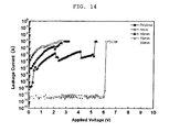
- FIG. 13 is a graph showing I(current)-V(voltage) of the HMDSO:DMB formed according to Example 3 in accordance with plasma treatment time.
- Example 4 was conducted in the same manner as in Example 3 except that He gas was used as the carrier gas for the additional plasma treatment on the plasma polymerized thin film deposited according to Example 1.
- FIG. 14 is a graph showing I(current)-V(voltage) of the HMDSO:DMB according to Example 4 in accordance with time.
- I-V properties of both thin films treated by H2/He and He plasma were improved without decreasing the thin films thickness.
- the plasma polymerized thin film according to the present invention can be seen to be superior in terms of dielectric properties, uniform thin-film thickness, thermal stability, uniform chemical bonding structure, hardness, elastic modulus and insulating property.
- the present invention provides a low dielectric constant plasma polymerized thin film and a method of manufacturing the same.
- the low dielectric constant thin film having a considerably low dielectric constant can be manufactured using linear organic/inorganic precursors, and further, a complicated process for pretreatment and post-treatment arising in the case of a spin casting process can be reduced. Furthermore, because annealing using an RTA apparatus is conducted, the dielectric constant and mechanical properties of the plasma polymerized thin film can be improved.
Applications Claiming Priority (1)
| Application Number | Priority Date | Filing Date | Title |
|---|---|---|---|
| KR1020070126331A KR100962044B1 (ko) | 2007-12-06 | 2007-12-06 | 저유전 플라즈마 중합체 박막 및 그 제조 방법 |
Publications (3)
| Publication Number | Publication Date |
|---|---|
| EP2070601A2 EP2070601A2 (en) | 2009-06-17 |
| EP2070601A3 EP2070601A3 (en) | 2010-02-24 |
| EP2070601B1 true EP2070601B1 (en) | 2012-05-02 |
Family
ID=40382806
Family Applications (1)
| Application Number | Title | Priority Date | Filing Date |
|---|---|---|---|
| EP08170636A Active EP2070601B1 (en) | 2007-12-06 | 2008-12-04 | Low dielectric constant plasma polymerized thin film and manufacturing method thereof |
Country Status (5)
Families Citing this family (7)
| Publication number | Priority date | Publication date | Assignee | Title |
|---|---|---|---|---|
| EP2744364B1 (en) | 2011-08-15 | 2016-10-26 | The Procter and Gamble Company | Cosmetic applicators |
| US9371430B2 (en) | 2013-08-19 | 2016-06-21 | Research & Business Foundation Sungkyunkwan University | Porous film with high hardness and a low dielectric constant and preparation method thereof |
| CN110540648A (zh) * | 2014-11-07 | 2019-12-06 | 中国科学院上海有机化学研究所 | 含苯并环丁烯基团的有机硅氧烷及其制备和应用 |
| US10351729B2 (en) | 2016-03-03 | 2019-07-16 | Motorola Mobility Llc | Polysiloxane films and methods of making polysiloxane films |
| CN108933088B (zh) * | 2017-05-25 | 2020-05-29 | 上海稷以科技有限公司 | 一种封装的方法及封装结构 |
| KR102578827B1 (ko) | 2018-04-24 | 2023-09-15 | 삼성전자주식회사 | 유연한 유무기 보호막 및 그 제조방법 |
| KR102138102B1 (ko) * | 2018-09-05 | 2020-07-27 | 성균관대학교산학협력단 | 저유전 플라즈마 중합체 박막 및 이의 제조 방법 |
Family Cites Families (35)
| Publication number | Priority date | Publication date | Assignee | Title |
|---|---|---|---|---|
| US5000113A (en) * | 1986-12-19 | 1991-03-19 | Applied Materials, Inc. | Thermal CVD/PECVD reactor and use for thermal chemical vapor deposition of silicon dioxide and in-situ multi-step planarized process |
| US4894532A (en) * | 1988-03-28 | 1990-01-16 | Westinghouse Electric Corp. | Optical fiber sensor with light absorbing moisture-sensitive coating |
| US4877641A (en) * | 1988-05-31 | 1989-10-31 | Olin Corporation | Process for plasma depositing silicon nitride and silicon dioxide films onto a substrate |
| US5203956A (en) * | 1990-01-08 | 1993-04-20 | Lsi Logic Corporation | Method for performing in-situ etch of a CVD chamber |
| US5288325A (en) * | 1991-03-29 | 1994-02-22 | Nec Corporation | Chemical vapor deposition apparatus |
| JP2703694B2 (ja) * | 1992-05-28 | 1998-01-26 | 信越半導体株式会社 | ガス供給装置 |
| JPH06240456A (ja) * | 1992-12-21 | 1994-08-30 | Kawasaki Steel Corp | 半導体装置のアルミニウム配線の形成方法及び装置 |
| US5444217A (en) * | 1993-01-21 | 1995-08-22 | Moore Epitaxial Inc. | Rapid thermal processing apparatus for processing semiconductor wafers |
| JPH06333857A (ja) * | 1993-05-27 | 1994-12-02 | Semiconductor Energy Lab Co Ltd | 成膜装置および成膜方法 |
| US6303523B2 (en) | 1998-02-11 | 2001-10-16 | Applied Materials, Inc. | Plasma processes for depositing low dielectric constant films |
| US6147009A (en) | 1998-06-29 | 2000-11-14 | International Business Machines Corporation | Hydrogenated oxidized silicon carbon material |
| US6312793B1 (en) * | 1999-05-26 | 2001-11-06 | International Business Machines Corporation | Multiphase low dielectric constant material |
| TW425635B (en) * | 1999-08-23 | 2001-03-11 | Promos Technologies Inc | Rapid thermal processing method and its device |
| EP1149933A1 (en) * | 2000-04-28 | 2001-10-31 | STMicroelectronics S.r.l. | Deposition method of dielectric films having a low dielectric constant |
| DE10034737C2 (de) * | 2000-07-17 | 2002-07-11 | Fraunhofer Ges Forschung | Verfahren zur Herstellung einer permanenten Entformungsschicht durch Plasmapolymerisation auf der Oberfläche eines Formteilwerkzeugs, ein nach dem Verfahren herstellbares Formteilwerkzeug und dessen Verwendung |
| US6441491B1 (en) * | 2000-10-25 | 2002-08-27 | International Business Machines Corporation | Ultralow dielectric constant material as an intralevel or interlevel dielectric in a semiconductor device and electronic device containing the same |
| US6486082B1 (en) * | 2001-06-18 | 2002-11-26 | Applied Materials, Inc. | CVD plasma assisted lower dielectric constant sicoh film |
| KR20030002993A (ko) * | 2001-06-29 | 2003-01-09 | 학교법인 포항공과대학교 | 저유전체 박막의 제조방법 |
| US20040058090A1 (en) * | 2001-09-14 | 2004-03-25 | Carlo Waldfried | Low temperature UV pretreating of porous low-k materials |
| DE60322347D1 (de) * | 2002-02-05 | 2008-09-04 | Dow Global Technologies Inc | Chemische dampfphasenabscheidung auf einem substrat mittels eines korona-plasmas |
| US6797643B2 (en) | 2002-10-23 | 2004-09-28 | Applied Materials Inc. | Plasma enhanced CVD low k carbon-doped silicon oxide film deposition using VHF-RF power |
| TWI282124B (en) * | 2002-11-28 | 2007-06-01 | Tosoh Corp | Insulating film material containing an organic silane compound, its production method and semiconductor device |
| US7288292B2 (en) | 2003-03-18 | 2007-10-30 | International Business Machines Corporation | Ultra low k (ULK) SiCOH film and method |
| US20040197474A1 (en) * | 2003-04-01 | 2004-10-07 | Vrtis Raymond Nicholas | Method for enhancing deposition rate of chemical vapor deposition films |
| US8137764B2 (en) | 2003-05-29 | 2012-03-20 | Air Products And Chemicals, Inc. | Mechanical enhancer additives for low dielectric films |
| US7611996B2 (en) * | 2004-03-31 | 2009-11-03 | Applied Materials, Inc. | Multi-stage curing of low K nano-porous films |
| US7491658B2 (en) * | 2004-10-13 | 2009-02-17 | International Business Machines Corporation | Ultra low k plasma enhanced chemical vapor deposition processes using a single bifunctional precursor containing both a SiCOH matrix functionality and organic porogen functionality |
| US7678712B2 (en) * | 2005-03-22 | 2010-03-16 | Honeywell International, Inc. | Vapor phase treatment of dielectric materials |
| US7901743B2 (en) | 2005-09-30 | 2011-03-08 | Tokyo Electron Limited | Plasma-assisted vapor phase treatment of low dielectric constant films using a batch processing system |
| US7381659B2 (en) * | 2005-11-22 | 2008-06-03 | International Business Machines Corporation | Method for reducing film stress for SiCOH low-k dielectric materials |
| US20070173071A1 (en) * | 2006-01-20 | 2007-07-26 | International Business Machines Corporation | SiCOH dielectric |
| US20070190808A1 (en) | 2006-02-10 | 2007-08-16 | Stowell Michael W | Low-k dielectric layers for large substrates |
| JP2007221039A (ja) | 2006-02-20 | 2007-08-30 | National Institute For Materials Science | 絶縁膜および絶縁膜材料 |
| KR100845941B1 (ko) | 2007-03-27 | 2008-07-14 | 성균관대학교산학협력단 | 저유전 상수값을 갖는 박막 제조 방법 및 이에 의하여제조된 박막 |
| KR100765806B1 (ko) * | 2007-04-23 | 2007-10-15 | 주식회사 아토 | 비정질탄소막 증착 방법 |
-
2007
- 2007-12-06 KR KR1020070126331A patent/KR100962044B1/ko not_active IP Right Cessation
-
2008
- 2008-08-14 US US12/228,668 patent/US7897521B2/en active Active
- 2008-12-04 AT AT08170636T patent/ATE555859T1/de active
- 2008-12-04 EP EP08170636A patent/EP2070601B1/en active Active
- 2008-12-05 CN CN2008101825701A patent/CN101450995B/zh active Active
Also Published As
| Publication number | Publication date |
|---|---|
| KR100962044B1 (ko) | 2010-06-08 |
| CN101450995B (zh) | 2012-05-09 |
| KR20090059462A (ko) | 2009-06-11 |
| EP2070601A2 (en) | 2009-06-17 |
| EP2070601A3 (en) | 2010-02-24 |
| ATE555859T1 (de) | 2012-05-15 |
| US20090054612A1 (en) | 2009-02-26 |
| US7897521B2 (en) | 2011-03-01 |
| CN101450995A (zh) | 2009-06-10 |
Similar Documents
| Publication | Publication Date | Title |
|---|---|---|
| EP2070601B1 (en) | Low dielectric constant plasma polymerized thin film and manufacturing method thereof | |
| US6383955B1 (en) | Silicone polymer insulation film on semiconductor substrate and method for forming the film | |
| JP3726226B2 (ja) | 絶縁膜及びその製造方法 | |
| US6455445B2 (en) | Silicone polymer insulation film on semiconductor substrate and method for forming the film | |
| KR101732187B1 (ko) | 플라즈마 강화된 화학기상 증착법에 의해 규소-질소 결합을 갖는 등각성 유전체 막을 형성하는 방법 | |
| US6432846B1 (en) | Silicone polymer insulation film on semiconductor substrate and method for forming the film | |
| US7354873B2 (en) | Method for forming insulation film | |
| CN101316945B (zh) | 低介电常数薄膜的灰化/湿法蚀刻损伤的抵抗性以及整体稳定性的改进方法 | |
| US20020076944A1 (en) | Organosilane CVD precursors and their use for making organosilane polymer low-k dielectric film | |
| US20110206857A1 (en) | Ultra low dielectric materials using hybrid precursors containing silicon with organic functional groups by plasma-enhanced chemical vapor deposition | |
| KR20000068308A (ko) | 반도체기판상에평탄한유전체층을침전시키는장치및방법 | |
| WO2005098085A2 (en) | Multi-stage curing of low k nano-porous films | |
| WO2006024017A1 (en) | Low temperature process to produce low-k dielectrics with low stress by plasma-enhanced chemical vapor deposition (pecvd) | |
| WO2010090038A1 (ja) | 絶縁膜材料、この絶縁膜材料を用いた成膜方法および絶縁膜 | |
| KR100987183B1 (ko) | 저유전 플라즈마 중합체 박막 및 그 제조 방법 | |
| KR100845941B1 (ko) | 저유전 상수값을 갖는 박막 제조 방법 및 이에 의하여제조된 박막 | |
| KR101506801B1 (ko) | 고강도 저유전 플라즈마 중합체 박막 및 그 제조 방법 | |
| US10968364B2 (en) | Plasma polymerized thin film having low dielectric constant, device, and method of preparing thin film | |
| US9371430B2 (en) | Porous film with high hardness and a low dielectric constant and preparation method thereof | |
| JP3197008B2 (ja) | 半導体基板上のシリコン重合体絶縁膜及びその膜を形成する方法 | |
| KR100697669B1 (ko) | 저유전 플라스마 중합체 박막의 제조 방법 및 이로부터제조된 저유전 박막 | |
| JP3814797B2 (ja) | 半導体基板上のシリコン重合体絶縁膜を形成する方法 | |
| US20100151151A1 (en) | Method of forming low-k film having chemical resistance | |
| KR20230113130A (ko) | 플라즈마 중합체 박막 및 이의 제조 방법 | |
| Kim et al. | Effects of ultraviolet irradiation treatment on low-k SiOC (− H) ultra-thin films deposited by using TMS/O 2 PEALD |
Legal Events
| Date | Code | Title | Description |
|---|---|---|---|
| PUAI | Public reference made under article 153(3) epc to a published international application that has entered the european phase |
Free format text: ORIGINAL CODE: 0009012 |
|
| 17P | Request for examination filed |
Effective date: 20081204 |
|
| AK | Designated contracting states |
Kind code of ref document: A2 Designated state(s): AT BE BG CH CY CZ DE DK EE ES FI FR GB GR HR HU IE IS IT LI LT LU LV MC MT NL NO PL PT RO SE SI SK TR |
|
| AX | Request for extension of the european patent |
Extension state: AL BA MK RS |
|
| PUAL | Search report despatched |
Free format text: ORIGINAL CODE: 0009013 |
|
| AK | Designated contracting states |
Kind code of ref document: A3 Designated state(s): AT BE BG CH CY CZ DE DK EE ES FI FR GB GR HR HU IE IS IT LI LT LU LV MC MT NL NO PL PT RO SE SI SK TR |
|
| AX | Request for extension of the european patent |
Extension state: AL BA MK RS |
|
| 17Q | First examination report despatched |
Effective date: 20101122 |
|
| GRAP | Despatch of communication of intention to grant a patent |
Free format text: ORIGINAL CODE: EPIDOSNIGR1 |
|
| RIN1 | Information on inventor provided before grant (corrected) |
Inventor name: JUNG, DONGGEUN Inventor name: WOO, JIHYUNG Inventor name: LEE, SUNGWOO |
|
| GRAS | Grant fee paid |
Free format text: ORIGINAL CODE: EPIDOSNIGR3 |
|
| GRAA | (expected) grant |
Free format text: ORIGINAL CODE: 0009210 |
|
| AK | Designated contracting states |
Kind code of ref document: B1 Designated state(s): AT BE BG CH CY CZ DE DK EE ES FI FR GB GR HR HU IE IS IT LI LT LU LV MC MT NL NO PL PT RO SE SI SK TR |
|
| REG | Reference to a national code |
Ref country code: GB Ref legal event code: FG4D |
|
| REG | Reference to a national code |
Ref country code: CH Ref legal event code: EP Ref country code: AT Ref legal event code: REF Ref document number: 555859 Country of ref document: AT Kind code of ref document: T Effective date: 20120515 |
|
| REG | Reference to a national code |
Ref country code: IE Ref legal event code: FG4D |
|
| REG | Reference to a national code |
Ref country code: DE Ref legal event code: R096 Ref document number: 602008015330 Country of ref document: DE Effective date: 20120705 |
|
| REG | Reference to a national code |
Ref country code: NL Ref legal event code: VDEP Effective date: 20120502 |
|
| REG | Reference to a national code |
Ref country code: LT Ref legal event code: MG4D Effective date: 20120502 |
|
| PG25 | Lapsed in a contracting state [announced via postgrant information from national office to epo] |
Ref country code: IS Free format text: LAPSE BECAUSE OF FAILURE TO SUBMIT A TRANSLATION OF THE DESCRIPTION OR TO PAY THE FEE WITHIN THE PRESCRIBED TIME-LIMIT Effective date: 20120902 Ref country code: NO Free format text: LAPSE BECAUSE OF FAILURE TO SUBMIT A TRANSLATION OF THE DESCRIPTION OR TO PAY THE FEE WITHIN THE PRESCRIBED TIME-LIMIT Effective date: 20120802 Ref country code: FI Free format text: LAPSE BECAUSE OF FAILURE TO SUBMIT A TRANSLATION OF THE DESCRIPTION OR TO PAY THE FEE WITHIN THE PRESCRIBED TIME-LIMIT Effective date: 20120502 Ref country code: CY Free format text: LAPSE BECAUSE OF FAILURE TO SUBMIT A TRANSLATION OF THE DESCRIPTION OR TO PAY THE FEE WITHIN THE PRESCRIBED TIME-LIMIT Effective date: 20120502 Ref country code: LT Free format text: LAPSE BECAUSE OF FAILURE TO SUBMIT A TRANSLATION OF THE DESCRIPTION OR TO PAY THE FEE WITHIN THE PRESCRIBED TIME-LIMIT Effective date: 20120502 Ref country code: SE Free format text: LAPSE BECAUSE OF FAILURE TO SUBMIT A TRANSLATION OF THE DESCRIPTION OR TO PAY THE FEE WITHIN THE PRESCRIBED TIME-LIMIT Effective date: 20120502 Ref country code: PL Free format text: LAPSE BECAUSE OF FAILURE TO SUBMIT A TRANSLATION OF THE DESCRIPTION OR TO PAY THE FEE WITHIN THE PRESCRIBED TIME-LIMIT Effective date: 20120502 |
|
| REG | Reference to a national code |
Ref country code: AT Ref legal event code: MK05 Ref document number: 555859 Country of ref document: AT Kind code of ref document: T Effective date: 20120502 |
|
| PG25 | Lapsed in a contracting state [announced via postgrant information from national office to epo] |
Ref country code: HR Free format text: LAPSE BECAUSE OF FAILURE TO SUBMIT A TRANSLATION OF THE DESCRIPTION OR TO PAY THE FEE WITHIN THE PRESCRIBED TIME-LIMIT Effective date: 20120502 Ref country code: LV Free format text: LAPSE BECAUSE OF FAILURE TO SUBMIT A TRANSLATION OF THE DESCRIPTION OR TO PAY THE FEE WITHIN THE PRESCRIBED TIME-LIMIT Effective date: 20120502 Ref country code: GR Free format text: LAPSE BECAUSE OF FAILURE TO SUBMIT A TRANSLATION OF THE DESCRIPTION OR TO PAY THE FEE WITHIN THE PRESCRIBED TIME-LIMIT Effective date: 20120803 Ref country code: SI Free format text: LAPSE BECAUSE OF FAILURE TO SUBMIT A TRANSLATION OF THE DESCRIPTION OR TO PAY THE FEE WITHIN THE PRESCRIBED TIME-LIMIT Effective date: 20120502 Ref country code: PT Free format text: LAPSE BECAUSE OF FAILURE TO SUBMIT A TRANSLATION OF THE DESCRIPTION OR TO PAY THE FEE WITHIN THE PRESCRIBED TIME-LIMIT Effective date: 20120903 |
|
| PG25 | Lapsed in a contracting state [announced via postgrant information from national office to epo] |
Ref country code: BE Free format text: LAPSE BECAUSE OF FAILURE TO SUBMIT A TRANSLATION OF THE DESCRIPTION OR TO PAY THE FEE WITHIN THE PRESCRIBED TIME-LIMIT Effective date: 20120502 |
|
| PGFP | Annual fee paid to national office [announced via postgrant information from national office to epo] |
Ref country code: LU Payment date: 20121126 Year of fee payment: 5 |
|
| PG25 | Lapsed in a contracting state [announced via postgrant information from national office to epo] |
Ref country code: AT Free format text: LAPSE BECAUSE OF FAILURE TO SUBMIT A TRANSLATION OF THE DESCRIPTION OR TO PAY THE FEE WITHIN THE PRESCRIBED TIME-LIMIT Effective date: 20120502 Ref country code: SK Free format text: LAPSE BECAUSE OF FAILURE TO SUBMIT A TRANSLATION OF THE DESCRIPTION OR TO PAY THE FEE WITHIN THE PRESCRIBED TIME-LIMIT Effective date: 20120502 Ref country code: NL Free format text: LAPSE BECAUSE OF FAILURE TO SUBMIT A TRANSLATION OF THE DESCRIPTION OR TO PAY THE FEE WITHIN THE PRESCRIBED TIME-LIMIT Effective date: 20120502 Ref country code: DK Free format text: LAPSE BECAUSE OF FAILURE TO SUBMIT A TRANSLATION OF THE DESCRIPTION OR TO PAY THE FEE WITHIN THE PRESCRIBED TIME-LIMIT Effective date: 20120502 Ref country code: CZ Free format text: LAPSE BECAUSE OF FAILURE TO SUBMIT A TRANSLATION OF THE DESCRIPTION OR TO PAY THE FEE WITHIN THE PRESCRIBED TIME-LIMIT Effective date: 20120502 Ref country code: EE Free format text: LAPSE BECAUSE OF FAILURE TO SUBMIT A TRANSLATION OF THE DESCRIPTION OR TO PAY THE FEE WITHIN THE PRESCRIBED TIME-LIMIT Effective date: 20120502 Ref country code: RO Free format text: LAPSE BECAUSE OF FAILURE TO SUBMIT A TRANSLATION OF THE DESCRIPTION OR TO PAY THE FEE WITHIN THE PRESCRIBED TIME-LIMIT Effective date: 20120502 |
|
| PGFP | Annual fee paid to national office [announced via postgrant information from national office to epo] |
Ref country code: CH Payment date: 20121211 Year of fee payment: 5 Ref country code: MC Payment date: 20121120 Year of fee payment: 5 Ref country code: FR Payment date: 20121210 Year of fee payment: 5 Ref country code: IE Payment date: 20121127 Year of fee payment: 5 |
|
| PG25 | Lapsed in a contracting state [announced via postgrant information from national office to epo] |
Ref country code: IT Free format text: LAPSE BECAUSE OF FAILURE TO SUBMIT A TRANSLATION OF THE DESCRIPTION OR TO PAY THE FEE WITHIN THE PRESCRIBED TIME-LIMIT Effective date: 20120502 |
|
| PGFP | Annual fee paid to national office [announced via postgrant information from national office to epo] |
Ref country code: GB Payment date: 20121219 Year of fee payment: 5 |
|
| PLBE | No opposition filed within time limit |
Free format text: ORIGINAL CODE: 0009261 |
|
| STAA | Information on the status of an ep patent application or granted ep patent |
Free format text: STATUS: NO OPPOSITION FILED WITHIN TIME LIMIT |
|
| 26N | No opposition filed |
Effective date: 20130205 |
|
| PG25 | Lapsed in a contracting state [announced via postgrant information from national office to epo] |
Ref country code: ES Free format text: LAPSE BECAUSE OF FAILURE TO SUBMIT A TRANSLATION OF THE DESCRIPTION OR TO PAY THE FEE WITHIN THE PRESCRIBED TIME-LIMIT Effective date: 20120813 |
|
| REG | Reference to a national code |
Ref country code: DE Ref legal event code: R097 Ref document number: 602008015330 Country of ref document: DE Effective date: 20130205 |
|
| PG25 | Lapsed in a contracting state [announced via postgrant information from national office to epo] |
Ref country code: BG Free format text: LAPSE BECAUSE OF FAILURE TO SUBMIT A TRANSLATION OF THE DESCRIPTION OR TO PAY THE FEE WITHIN THE PRESCRIBED TIME-LIMIT Effective date: 20120802 |
|
| PG25 | Lapsed in a contracting state [announced via postgrant information from national office to epo] |
Ref country code: MT Free format text: LAPSE BECAUSE OF FAILURE TO SUBMIT A TRANSLATION OF THE DESCRIPTION OR TO PAY THE FEE WITHIN THE PRESCRIBED TIME-LIMIT Effective date: 20120502 |
|
| PG25 | Lapsed in a contracting state [announced via postgrant information from national office to epo] |
Ref country code: TR Free format text: LAPSE BECAUSE OF FAILURE TO SUBMIT A TRANSLATION OF THE DESCRIPTION OR TO PAY THE FEE WITHIN THE PRESCRIBED TIME-LIMIT Effective date: 20120502 |
|
| PG25 | Lapsed in a contracting state [announced via postgrant information from national office to epo] |
Ref country code: HU Free format text: LAPSE BECAUSE OF FAILURE TO SUBMIT A TRANSLATION OF THE DESCRIPTION OR TO PAY THE FEE WITHIN THE PRESCRIBED TIME-LIMIT Effective date: 20081204 Ref country code: MC Free format text: LAPSE BECAUSE OF NON-PAYMENT OF DUE FEES Effective date: 20131231 |
|
| REG | Reference to a national code |
Ref country code: CH Ref legal event code: PL |
|
| GBPC | Gb: european patent ceased through non-payment of renewal fee |
Effective date: 20131204 |
|
| PG25 | Lapsed in a contracting state [announced via postgrant information from national office to epo] |
Ref country code: LU Free format text: LAPSE BECAUSE OF NON-PAYMENT OF DUE FEES Effective date: 20131204 |
|
| REG | Reference to a national code |
Ref country code: IE Ref legal event code: MM4A |
|
| REG | Reference to a national code |
Ref country code: FR Ref legal event code: ST Effective date: 20140829 |
|
| PG25 | Lapsed in a contracting state [announced via postgrant information from national office to epo] |
Ref country code: CH Free format text: LAPSE BECAUSE OF NON-PAYMENT OF DUE FEES Effective date: 20131231 Ref country code: IE Free format text: LAPSE BECAUSE OF NON-PAYMENT OF DUE FEES Effective date: 20131204 Ref country code: LI Free format text: LAPSE BECAUSE OF NON-PAYMENT OF DUE FEES Effective date: 20131231 |
|
| PG25 | Lapsed in a contracting state [announced via postgrant information from national office to epo] |
Ref country code: FR Free format text: LAPSE BECAUSE OF NON-PAYMENT OF DUE FEES Effective date: 20131231 Ref country code: GB Free format text: LAPSE BECAUSE OF NON-PAYMENT OF DUE FEES Effective date: 20131204 |
|
| PGFP | Annual fee paid to national office [announced via postgrant information from national office to epo] |
Ref country code: DE Payment date: 20221011 Year of fee payment: 15 |