EP2053640A2 - Method and system for improving dielectric film quality for void free gap fill - Google Patents
Method and system for improving dielectric film quality for void free gap fill Download PDFInfo
- Publication number
- EP2053640A2 EP2053640A2 EP08167333A EP08167333A EP2053640A2 EP 2053640 A2 EP2053640 A2 EP 2053640A2 EP 08167333 A EP08167333 A EP 08167333A EP 08167333 A EP08167333 A EP 08167333A EP 2053640 A2 EP2053640 A2 EP 2053640A2
- Authority
- EP
- European Patent Office
- Prior art keywords
- oxide layer
- silicon oxide
- silicon
- substrate
- layer
- Prior art date
- Legal status (The legal status is an assumption and is not a legal conclusion. Google has not performed a legal analysis and makes no representation as to the accuracy of the status listed.)
- Withdrawn
Links
Images


Classifications
-
- C—CHEMISTRY; METALLURGY
- C23—COATING METALLIC MATERIAL; COATING MATERIAL WITH METALLIC MATERIAL; CHEMICAL SURFACE TREATMENT; DIFFUSION TREATMENT OF METALLIC MATERIAL; COATING BY VACUUM EVAPORATION, BY SPUTTERING, BY ION IMPLANTATION OR BY CHEMICAL VAPOUR DEPOSITION, IN GENERAL; INHIBITING CORROSION OF METALLIC MATERIAL OR INCRUSTATION IN GENERAL
- C23C—COATING METALLIC MATERIAL; COATING MATERIAL WITH METALLIC MATERIAL; SURFACE TREATMENT OF METALLIC MATERIAL BY DIFFUSION INTO THE SURFACE, BY CHEMICAL CONVERSION OR SUBSTITUTION; COATING BY VACUUM EVAPORATION, BY SPUTTERING, BY ION IMPLANTATION OR BY CHEMICAL VAPOUR DEPOSITION, IN GENERAL
- C23C16/00—Chemical coating by decomposition of gaseous compounds, without leaving reaction products of surface material in the coating, i.e. chemical vapour deposition [CVD] processes
- C23C16/04—Coating on selected surface areas, e.g. using masks
- C23C16/045—Coating cavities or hollow spaces, e.g. interior of tubes; Infiltration of porous substrates
-
- C—CHEMISTRY; METALLURGY
- C23—COATING METALLIC MATERIAL; COATING MATERIAL WITH METALLIC MATERIAL; CHEMICAL SURFACE TREATMENT; DIFFUSION TREATMENT OF METALLIC MATERIAL; COATING BY VACUUM EVAPORATION, BY SPUTTERING, BY ION IMPLANTATION OR BY CHEMICAL VAPOUR DEPOSITION, IN GENERAL; INHIBITING CORROSION OF METALLIC MATERIAL OR INCRUSTATION IN GENERAL
- C23C—COATING METALLIC MATERIAL; COATING MATERIAL WITH METALLIC MATERIAL; SURFACE TREATMENT OF METALLIC MATERIAL BY DIFFUSION INTO THE SURFACE, BY CHEMICAL CONVERSION OR SUBSTITUTION; COATING BY VACUUM EVAPORATION, BY SPUTTERING, BY ION IMPLANTATION OR BY CHEMICAL VAPOUR DEPOSITION, IN GENERAL
- C23C16/00—Chemical coating by decomposition of gaseous compounds, without leaving reaction products of surface material in the coating, i.e. chemical vapour deposition [CVD] processes
- C23C16/22—Chemical coating by decomposition of gaseous compounds, without leaving reaction products of surface material in the coating, i.e. chemical vapour deposition [CVD] processes characterised by the deposition of inorganic material, other than metallic material
- C23C16/24—Deposition of silicon only
-
- C—CHEMISTRY; METALLURGY
- C23—COATING METALLIC MATERIAL; COATING MATERIAL WITH METALLIC MATERIAL; CHEMICAL SURFACE TREATMENT; DIFFUSION TREATMENT OF METALLIC MATERIAL; COATING BY VACUUM EVAPORATION, BY SPUTTERING, BY ION IMPLANTATION OR BY CHEMICAL VAPOUR DEPOSITION, IN GENERAL; INHIBITING CORROSION OF METALLIC MATERIAL OR INCRUSTATION IN GENERAL
- C23C—COATING METALLIC MATERIAL; COATING MATERIAL WITH METALLIC MATERIAL; SURFACE TREATMENT OF METALLIC MATERIAL BY DIFFUSION INTO THE SURFACE, BY CHEMICAL CONVERSION OR SUBSTITUTION; COATING BY VACUUM EVAPORATION, BY SPUTTERING, BY ION IMPLANTATION OR BY CHEMICAL VAPOUR DEPOSITION, IN GENERAL
- C23C16/00—Chemical coating by decomposition of gaseous compounds, without leaving reaction products of surface material in the coating, i.e. chemical vapour deposition [CVD] processes
- C23C16/22—Chemical coating by decomposition of gaseous compounds, without leaving reaction products of surface material in the coating, i.e. chemical vapour deposition [CVD] processes characterised by the deposition of inorganic material, other than metallic material
- C23C16/30—Deposition of compounds, mixtures or solid solutions, e.g. borides, carbides, nitrides
- C23C16/40—Oxides
- C23C16/401—Oxides containing silicon
-
- C—CHEMISTRY; METALLURGY
- C23—COATING METALLIC MATERIAL; COATING MATERIAL WITH METALLIC MATERIAL; CHEMICAL SURFACE TREATMENT; DIFFUSION TREATMENT OF METALLIC MATERIAL; COATING BY VACUUM EVAPORATION, BY SPUTTERING, BY ION IMPLANTATION OR BY CHEMICAL VAPOUR DEPOSITION, IN GENERAL; INHIBITING CORROSION OF METALLIC MATERIAL OR INCRUSTATION IN GENERAL
- C23C—COATING METALLIC MATERIAL; COATING MATERIAL WITH METALLIC MATERIAL; SURFACE TREATMENT OF METALLIC MATERIAL BY DIFFUSION INTO THE SURFACE, BY CHEMICAL CONVERSION OR SUBSTITUTION; COATING BY VACUUM EVAPORATION, BY SPUTTERING, BY ION IMPLANTATION OR BY CHEMICAL VAPOUR DEPOSITION, IN GENERAL
- C23C16/00—Chemical coating by decomposition of gaseous compounds, without leaving reaction products of surface material in the coating, i.e. chemical vapour deposition [CVD] processes
- C23C16/56—After-treatment
-
- H—ELECTRICITY
- H10—SEMICONDUCTOR DEVICES; ELECTRIC SOLID-STATE DEVICES NOT OTHERWISE PROVIDED FOR
- H10P—GENERIC PROCESSES OR APPARATUS FOR THE MANUFACTURE OR TREATMENT OF DEVICES COVERED BY CLASS H10
- H10P14/00—Formation of materials, e.g. in the shape of layers or pillars
- H10P14/60—Formation of materials, e.g. in the shape of layers or pillars of insulating materials
- H10P14/65—Formation of materials, e.g. in the shape of layers or pillars of insulating materials characterised by treatments performed before or after the formation of the materials
- H10P14/6516—Formation of materials, e.g. in the shape of layers or pillars of insulating materials characterised by treatments performed before or after the formation of the materials of treatments performed after formation of the materials
- H10P14/6529—Formation of materials, e.g. in the shape of layers or pillars of insulating materials characterised by treatments performed before or after the formation of the materials of treatments performed after formation of the materials by exposure to a gas or vapour
-
- H—ELECTRICITY
- H10—SEMICONDUCTOR DEVICES; ELECTRIC SOLID-STATE DEVICES NOT OTHERWISE PROVIDED FOR
- H10P—GENERIC PROCESSES OR APPARATUS FOR THE MANUFACTURE OR TREATMENT OF DEVICES COVERED BY CLASS H10
- H10P14/00—Formation of materials, e.g. in the shape of layers or pillars
- H10P14/60—Formation of materials, e.g. in the shape of layers or pillars of insulating materials
- H10P14/65—Formation of materials, e.g. in the shape of layers or pillars of insulating materials characterised by treatments performed before or after the formation of the materials
- H10P14/6516—Formation of materials, e.g. in the shape of layers or pillars of insulating materials characterised by treatments performed before or after the formation of the materials of treatments performed after formation of the materials
- H10P14/6529—Formation of materials, e.g. in the shape of layers or pillars of insulating materials characterised by treatments performed before or after the formation of the materials of treatments performed after formation of the materials by exposure to a gas or vapour
- H10P14/6532—Formation of materials, e.g. in the shape of layers or pillars of insulating materials characterised by treatments performed before or after the formation of the materials of treatments performed after formation of the materials by exposure to a gas or vapour by exposure to a plasma
-
- H—ELECTRICITY
- H10—SEMICONDUCTOR DEVICES; ELECTRIC SOLID-STATE DEVICES NOT OTHERWISE PROVIDED FOR
- H10P—GENERIC PROCESSES OR APPARATUS FOR THE MANUFACTURE OR TREATMENT OF DEVICES COVERED BY CLASS H10
- H10P14/00—Formation of materials, e.g. in the shape of layers or pillars
- H10P14/60—Formation of materials, e.g. in the shape of layers or pillars of insulating materials
- H10P14/63—Formation of materials, e.g. in the shape of layers or pillars of insulating materials characterised by the formation processes
- H10P14/6326—Deposition processes
- H10P14/6328—Deposition from the gas or vapour phase
- H10P14/6334—Deposition from the gas or vapour phase using decomposition or reaction of gaseous or vapour phase compounds, i.e. chemical vapour deposition
- H10P14/6336—Deposition from the gas or vapour phase using decomposition or reaction of gaseous or vapour phase compounds, i.e. chemical vapour deposition in the presence of a plasma [PECVD]
-
- H—ELECTRICITY
- H10—SEMICONDUCTOR DEVICES; ELECTRIC SOLID-STATE DEVICES NOT OTHERWISE PROVIDED FOR
- H10P—GENERIC PROCESSES OR APPARATUS FOR THE MANUFACTURE OR TREATMENT OF DEVICES COVERED BY CLASS H10
- H10P14/00—Formation of materials, e.g. in the shape of layers or pillars
- H10P14/60—Formation of materials, e.g. in the shape of layers or pillars of insulating materials
- H10P14/63—Formation of materials, e.g. in the shape of layers or pillars of insulating materials characterised by the formation processes
- H10P14/6326—Deposition processes
- H10P14/6328—Deposition from the gas or vapour phase
- H10P14/6334—Deposition from the gas or vapour phase using decomposition or reaction of gaseous or vapour phase compounds, i.e. chemical vapour deposition
- H10P14/6339—Deposition from the gas or vapour phase using decomposition or reaction of gaseous or vapour phase compounds, i.e. chemical vapour deposition deposition by cyclic CVD, e.g. ALD, ALE or pulsed CVD
-
- H—ELECTRICITY
- H10—SEMICONDUCTOR DEVICES; ELECTRIC SOLID-STATE DEVICES NOT OTHERWISE PROVIDED FOR
- H10P—GENERIC PROCESSES OR APPARATUS FOR THE MANUFACTURE OR TREATMENT OF DEVICES COVERED BY CLASS H10
- H10P14/00—Formation of materials, e.g. in the shape of layers or pillars
- H10P14/60—Formation of materials, e.g. in the shape of layers or pillars of insulating materials
- H10P14/65—Formation of materials, e.g. in the shape of layers or pillars of insulating materials characterised by treatments performed before or after the formation of the materials
- H10P14/6516—Formation of materials, e.g. in the shape of layers or pillars of insulating materials characterised by treatments performed before or after the formation of the materials of treatments performed after formation of the materials
- H10P14/6518—Formation of materials, e.g. in the shape of layers or pillars of insulating materials characterised by treatments performed before or after the formation of the materials of treatments performed after formation of the materials by introduction of substances into an already-existing insulating layer
- H10P14/6519—Formation of materials, e.g. in the shape of layers or pillars of insulating materials characterised by treatments performed before or after the formation of the materials of treatments performed after formation of the materials by introduction of substances into an already-existing insulating layer the substance being oxygen
-
- H—ELECTRICITY
- H10—SEMICONDUCTOR DEVICES; ELECTRIC SOLID-STATE DEVICES NOT OTHERWISE PROVIDED FOR
- H10P—GENERIC PROCESSES OR APPARATUS FOR THE MANUFACTURE OR TREATMENT OF DEVICES COVERED BY CLASS H10
- H10P14/00—Formation of materials, e.g. in the shape of layers or pillars
- H10P14/60—Formation of materials, e.g. in the shape of layers or pillars of insulating materials
- H10P14/66—Formation of materials, e.g. in the shape of layers or pillars of insulating materials characterised by the type of materials
- H10P14/668—Formation of materials, e.g. in the shape of layers or pillars of insulating materials characterised by the type of materials the materials being characterised by the deposition precursor materials
- H10P14/6681—Formation of materials, e.g. in the shape of layers or pillars of insulating materials characterised by the type of materials the materials being characterised by the deposition precursor materials the precursor containing a compound comprising Si
- H10P14/6682—Formation of materials, e.g. in the shape of layers or pillars of insulating materials characterised by the type of materials the materials being characterised by the deposition precursor materials the precursor containing a compound comprising Si the compound being a silane, e.g. disilane, methylsilane or chlorosilane
-
- H—ELECTRICITY
- H10—SEMICONDUCTOR DEVICES; ELECTRIC SOLID-STATE DEVICES NOT OTHERWISE PROVIDED FOR
- H10P—GENERIC PROCESSES OR APPARATUS FOR THE MANUFACTURE OR TREATMENT OF DEVICES COVERED BY CLASS H10
- H10P14/00—Formation of materials, e.g. in the shape of layers or pillars
- H10P14/60—Formation of materials, e.g. in the shape of layers or pillars of insulating materials
- H10P14/66—Formation of materials, e.g. in the shape of layers or pillars of insulating materials characterised by the type of materials
- H10P14/668—Formation of materials, e.g. in the shape of layers or pillars of insulating materials characterised by the type of materials the materials being characterised by the deposition precursor materials
- H10P14/6681—Formation of materials, e.g. in the shape of layers or pillars of insulating materials characterised by the type of materials the materials being characterised by the deposition precursor materials the precursor containing a compound comprising Si
- H10P14/6687—Formation of materials, e.g. in the shape of layers or pillars of insulating materials characterised by the type of materials the materials being characterised by the deposition precursor materials the precursor containing a compound comprising Si the compound comprising silicon and nitrogen
-
- H—ELECTRICITY
- H10—SEMICONDUCTOR DEVICES; ELECTRIC SOLID-STATE DEVICES NOT OTHERWISE PROVIDED FOR
- H10P—GENERIC PROCESSES OR APPARATUS FOR THE MANUFACTURE OR TREATMENT OF DEVICES COVERED BY CLASS H10
- H10P14/00—Formation of materials, e.g. in the shape of layers or pillars
- H10P14/60—Formation of materials, e.g. in the shape of layers or pillars of insulating materials
- H10P14/69—Inorganic materials
- H10P14/692—Inorganic materials composed of oxides, glassy oxides or oxide-based glasses
- H10P14/6921—Inorganic materials composed of oxides, glassy oxides or oxide-based glasses containing silicon
- H10P14/69215—Inorganic materials composed of oxides, glassy oxides or oxide-based glasses containing silicon the material being a silicon oxide, e.g. SiO2
-
- H—ELECTRICITY
- H10—SEMICONDUCTOR DEVICES; ELECTRIC SOLID-STATE DEVICES NOT OTHERWISE PROVIDED FOR
- H10P—GENERIC PROCESSES OR APPARATUS FOR THE MANUFACTURE OR TREATMENT OF DEVICES COVERED BY CLASS H10
- H10P14/00—Formation of materials, e.g. in the shape of layers or pillars
- H10P14/60—Formation of materials, e.g. in the shape of layers or pillars of insulating materials
- H10P14/69—Inorganic materials
- H10P14/692—Inorganic materials composed of oxides, glassy oxides or oxide-based glasses
- H10P14/6921—Inorganic materials composed of oxides, glassy oxides or oxide-based glasses containing silicon
- H10P14/6922—Inorganic materials composed of oxides, glassy oxides or oxide-based glasses containing silicon the material containing Si, O and at least one of H, N, C, F or other non-metal elements, e.g. SiOC, SiOC:H or SiONC
-
- H—ELECTRICITY
- H10—SEMICONDUCTOR DEVICES; ELECTRIC SOLID-STATE DEVICES NOT OTHERWISE PROVIDED FOR
- H10P—GENERIC PROCESSES OR APPARATUS FOR THE MANUFACTURE OR TREATMENT OF DEVICES COVERED BY CLASS H10
- H10P14/00—Formation of materials, e.g. in the shape of layers or pillars
- H10P14/60—Formation of materials, e.g. in the shape of layers or pillars of insulating materials
- H10P14/69—Inorganic materials
- H10P14/692—Inorganic materials composed of oxides, glassy oxides or oxide-based glasses
- H10P14/6938—Inorganic materials composed of oxides, glassy oxides or oxide-based glasses the material containing at least one metal element, e.g. metal oxides, metal oxynitrides or metal oxycarbides
- H10P14/6939—Inorganic materials composed of oxides, glassy oxides or oxide-based glasses the material containing at least one metal element, e.g. metal oxides, metal oxynitrides or metal oxycarbides characterised by the metal
-
- H—ELECTRICITY
- H10—SEMICONDUCTOR DEVICES; ELECTRIC SOLID-STATE DEVICES NOT OTHERWISE PROVIDED FOR
- H10P—GENERIC PROCESSES OR APPARATUS FOR THE MANUFACTURE OR TREATMENT OF DEVICES COVERED BY CLASS H10
- H10P14/00—Formation of materials, e.g. in the shape of layers or pillars
- H10P14/60—Formation of materials, e.g. in the shape of layers or pillars of insulating materials
- H10P14/69—Inorganic materials
- H10P14/692—Inorganic materials composed of oxides, glassy oxides or oxide-based glasses
- H10P14/6938—Inorganic materials composed of oxides, glassy oxides or oxide-based glasses the material containing at least one metal element, e.g. metal oxides, metal oxynitrides or metal oxycarbides
- H10P14/6939—Inorganic materials composed of oxides, glassy oxides or oxide-based glasses the material containing at least one metal element, e.g. metal oxides, metal oxynitrides or metal oxycarbides characterised by the metal
- H10P14/69392—Inorganic materials composed of oxides, glassy oxides or oxide-based glasses the material containing at least one metal element, e.g. metal oxides, metal oxynitrides or metal oxycarbides characterised by the metal the material containing hafnium, e.g. HfO2
-
- H—ELECTRICITY
- H10—SEMICONDUCTOR DEVICES; ELECTRIC SOLID-STATE DEVICES NOT OTHERWISE PROVIDED FOR
- H10P—GENERIC PROCESSES OR APPARATUS FOR THE MANUFACTURE OR TREATMENT OF DEVICES COVERED BY CLASS H10
- H10P14/00—Formation of materials, e.g. in the shape of layers or pillars
- H10P14/60—Formation of materials, e.g. in the shape of layers or pillars of insulating materials
- H10P14/69—Inorganic materials
- H10P14/692—Inorganic materials composed of oxides, glassy oxides or oxide-based glasses
- H10P14/6938—Inorganic materials composed of oxides, glassy oxides or oxide-based glasses the material containing at least one metal element, e.g. metal oxides, metal oxynitrides or metal oxycarbides
- H10P14/6939—Inorganic materials composed of oxides, glassy oxides or oxide-based glasses the material containing at least one metal element, e.g. metal oxides, metal oxynitrides or metal oxycarbides characterised by the metal
- H10P14/69397—Inorganic materials composed of oxides, glassy oxides or oxide-based glasses the material containing at least one metal element, e.g. metal oxides, metal oxynitrides or metal oxycarbides characterised by the metal the material containing two or more metal elements
-
- H—ELECTRICITY
- H10—SEMICONDUCTOR DEVICES; ELECTRIC SOLID-STATE DEVICES NOT OTHERWISE PROVIDED FOR
- H10W—GENERIC PACKAGES, INTERCONNECTIONS, CONNECTORS OR OTHER CONSTRUCTIONAL DETAILS OF DEVICES COVERED BY CLASS H10
- H10W20/00—Interconnections in chips, wafers or substrates
- H10W20/01—Manufacture or treatment
- H10W20/071—Manufacture or treatment of dielectric parts thereof
- H10W20/098—Manufacture or treatment of dielectric parts thereof by filling between adjacent conductive parts
Definitions
- the present invention is directed to semiconductor thin film process techniques. Methods and system are described for improving quality of the dielectric film morphologically adapted over various device structures. More particularly, embodiments of the invention provide methods and system of forming silicon oxide film with increased density to achieve void free gap fill for trenches with high aspect ratio. For example, the invention is applied to form high quality silicon oxide films for filling narrow STI trenches, among other applications.
- STI shallow trench isolation
- An STI may include a trench or gap formed in an isolation region of a semiconductor substrate that is filled with a dielectric material to hinder the electrical coupling of nearby device structures (e . g ., transistors, diodes, etc .).
- device structures e . g ., transistors, diodes, etc .
- the vertical heights of the STI trenches normally do not decrease as fast as their horizontal widths, resulting in gaps and trenches with larger ratios of height to width ( i . e ., higher the aspect ratios).
- Voids and seams in a dielectric layer cause problems both during semiconductor device fabrication and in the finished devices.
- the voids and seams are formed randomly in the dielectric material and have unpredictable sizes, shapes, locations and densities. This results in unpredictable and inconsistent post-deposition processing of the layer, such as nonuniform etching, polishing, annealing, etc .
- the voids and seams in the finished devices also create variations in the dielectric qualities of gaps and trenches in device structures. This can result in erratic and inferior device performance due to electrical crosstalk, charge leakage, and in some instances, shorting within the device, among other problems.
- Another technique to control void formation is to increase the flowability of the deposited dielectric material.
- a material with more flowability can more quickly fill a void or seam and prevent it from becoming a permanent defect in the fill volume.
- highly flowable spin-on-glass (SOG) precursors like PSZ (Polysilazene), HSQ (Hydrosilsesequioxane) films, etc ., were conventionally employed for filling trenches with good gap-filling capabilities.
- SOG spin-on-glass
- One approach to increased film densification is to use high-temperature annealing when curing the SOG film into a silicon oxide film.
- the high-temperature annealing used to remove residual carbon species and OH groups may also cause a considerable degree of volumetric shrinkage of film.
- the as-deposited films are constrained and unable to shrink, resulting low density films with porous or void containing structures.
- the present invention is directed to semiconductor thin film process techniques. Methods and system are described for improving quality of the dielectric film morphologically adapted over various device structures. More particularly, embodiments of the invention provide methods and systems of forming silicon oxide film with increased density to achieve void free gap fill for trenches having a high aspect ratio. For example, the invention is applied to form high quality silicon oxide films for filling narrow STI trenches, among other applications.
- Embodiments of the present invention include methods of forming a silicon oxide layer on a substrate. These methods may include providing a substrate and forming a first silicon oxide layer overlying at least a portion of the substrate.
- the first silicon oxide layer includes residual water, hydroxyl groups, and carbon species.
- the methods may include exposing the first silicon oxide layer to a plurality of silicon-containing species during which at least a portion of the plurality of silicon-containing species either react with at least a portion of the residual water and hydroxyl groups, or are thermally decomposed to form a plurality of amorphous silicon components.
- the plurality of amorphous silicon components may be partially intermixed with the first silicon oxide layer.
- the methods may still further include annealing the first silicon oxide layer partially intermixed with the plurality of amorphous silicon components in an oxidative environment to form a second silicon oxide layer on the substrate. At least a portion of amorphous silicon components are oxidized to become part of the second silicon oxide layer, and unreacted residual hydroxyl groups and carbon species in the second silicon oxide layer are substantially removed.
- Embodiments of the invention also provide a method of forming a silicon oxide layer on a substrate.
- the method includes providing a substrate including one or more trenches in a semiconductor process chamber.
- the method further includes depositing a first silicon oxide layer including hydroxyl groups and carbon species on the substrate.
- the first silicon oxide layer at least partially fills the one or more trenches.
- the method includes introducing a plurality of silicon-containing particles in the semiconductor process chamber.
- the silicon-containing particles may be incorporated into the first silicon oxide layer.
- the method further includes forming a second silicon oxide layer by annealing the first silicon oxide layer, which includes the plurality of silicon-containing particles, in an oxidative environment.
- the plurality of silicon-containing particles are oxidized and the hydroxyl groups and carbon species are substantially removed.
- Embodiments of the invention additionally provide a method of forming a silicon oxide layer on a substrate.
- the method includes providing a substrate in a semiconductor process chamber.
- the substrate may include one or more trenches.
- the method further includes depositing a first silicon oxide layer including hydroxyl groups and carbon species on the substrate.
- the first silicon oxide layer at least partially fills the one or more trenches.
- the method includes introducing a plurality of silicon-containing particles in the semiconductor process chamber. The plurality of silicon-containing particles is incorporated into the first silicon oxide layer.
- introducing a plurality of silicon-containing particles is conducted by generating the silicon-containing particles from a silicon-rich precursor in a plasma and depositing the plasma-generated silicon-containing particles on the first silicon oxide layer by turning off the plasma for a predetermined time period. Furthermore, the method may include forming a second silicon oxide layer by annealing the first silicon oxide layer including the plurality of silicon-containing particles in an oxidative environment so that the plurality of silicon-containing particles are oxidized and the hydroxyl groups and carbon species may be substantially removed.
- the invention is also directed to a device for carrying out the disclosed methods and including device parts for performing each described method steps. These method steps may be performed by way of hardware components, a computer programmed by appropriate software, by any combination of the two or in any other manner. Furthermore, the invention is also directed to methods by which the described device operates. It includes method steps for carrying out every function of the device.
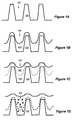
- FIGS. 1A-1D are simplified exemplary cross sectional views of processes of forming a silicon oxide layer on a substrate according to an embodiment of the present invention
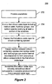
- FIG. 2 is a simplified flowchart showing a method of forming a silicon oxide layer on a substrate according to an embodiment of the present invention
- FIGS. 3A-3F are simplified exemplary cross sectional views of processes for alternating gap-fill oxide depositions and treatments according to another embodiment of the present invention.
- FIG. 4 is a simplified flowchart showing a method of forming a silicon oxide layer on a substrate according to an embodiment of the present invention
- FIGS. 5A-5D are simplified exemplary cross sectional views of processes forming a silicon oxide layer on a substrate according to an alternative embodiment of the present invention.
- FIG. 6 is a simplified flowchart showing a method of forming a silicon oxide layer on a substrate according to another embodiment of the present invention.
- FIG. 7 is a cross sectional view of an exemplary processing system according to an embodiment of the present invention.
- embodiments of the invention provide methods and system of forming silicon oxide film with increased density to achieve void free gap fill for trenches with a high aspect ratio.
- the invention may be applied to form high quality silicon oxide films for filling narrow STI trenches, among other applications.
- Flowable silicon dioxide films deposited by chemical vapor deposition techniques from silicon-containing precursors (e.g., organosilicates) and remote plasma generated atomic oxygen have been applied to STI applications.
- the as-deposited flowable oxide films may initially have relatively low film density due in part to ingredients like residual water and carbon species, as well as significant hydroxyl groups.
- silicon can be added.
- the residual carbon species and hydroxyl groups can react, resulting in significant film shrinkage and densification.
- the added silicon can counterbalance this shrinkage by expanding while it oxidizes in the same oxidizing atmosphere.
- compensating for the shrinkage of flowable oxide films substantially helps the formation of a dense silicon oxide film that achieves void free gap fill.
- FIGS. 1A-1D are simplified exemplary cross sectional views of processes for forming a silicon oxide layer on a substrate according to embodiments of the present invention. These diagrams are merely examples, and are not intended to restrict the invention to only what is illustrated. One of ordinary skill in the art would recognize other variations, modifications, and alternatives.
- FIGS. 1A-1D may be viewed in conjunction with FIG. 2 which is showing a method of forming a silicon oxide layer on a substrate according to an embodiment of the present invention.
- method 200 includes providing a substrate in process 202.
- the substrate is substrate 100 shown in FIGS. 1A-1D .
- the substrate 100 may be a semiconductor process wafer ( e .
- substrate 100 includes trench 102 having sidewalls and a bottom.
- the method 200 then includes a process of forming a silicon oxide layer overlying the at least a portion of the substrate (Process 204).
- silicon oxide layer 110 is formed overlying the substrate 100 provided in a semiconductor process chamber (an exemplary chamber can be seen in Figure 7 ).
- the silicon oxide layer 110 may be deposited by CVD-based approach using organosilicate precursors and atomic oxygen precursor generated by a remote plasma source as described in co-assigned U.S. Patent Application No.
- the as-deposited silicon oxide layer possesses a flow-like characteristic due to its ingredients including some residual water and carbon species as well as significant hydroxyl groups.
- the flow-like silicon oxide film may be used for STI applications. For example, shown in FIG.
- the sidewalls and bottom of trench 102 as well as substrate surface outside the trench are substantially covered by the formation of silicon oxide layer 110.
- the as-deposited silicon oxide layer 110 may extend from filling a partial depth of trench 102 to completely filling and extending over trench 102.
- silicon oxide layer 110 completely fills at least a portion of trench 102 with no voiding or seams.
- direct use of the as-deposited film by process 204 can result in a dielectric that is too porous and does not have an adequate mechanical strength.
- certain embodiments of the present invention are applied to perform further treatment of the as-deposited silicon oxide layer 110 to improve film quality with increased density and still achieve void free gap fill.
- the as-deposited silicon oxide film is exposed to a plurality of silicon-containing species (Process 206).
- the plurality of silicon-containing species can be introduced into the same semiconductor process chamber.
- the exposure of the silicon-containing species may be performed in a separate chamber other than the semiconductor process chamber for depositing silicon oxide layer (at process 204).
- the silicon-containing species includes one or a combination of following species: linear polysilanes (silane, disilane, and higher homologues), cyclic polysilanes (cyclopentasilane), dichlorosilane, tetrachlorosilane, and similar species.
- each of the silicon-containing species is in gas phase supplied from either a pure gas source or diluted with an inert gas, such as N 2 or He.
- an inert gas such as N 2 or He.
- Process 206 is carried under the following conditions including an exposure temperature varied from about room temperature to about 900 °C, e.g. from about 20 °C to about 900°C, an exposure pressure (of the gas-phase silicon-containing species) varied from about 10 mTorr to about 600 Torr, and an exposure time varied from about 1 second to about 3 hours.
- an exposure temperature varied from about room temperature to about 900 °C, e.g. from about 20 °C to about 900°C
- an exposure pressure (of the gas-phase silicon-containing species) varied from about 10 mTorr to about 600 Torr
- an exposure time varied from about 1 second to about 3 hours.
- these conditions may vary but should not unduly limit the scope of the claims herein.
- the exposure of the plurality of silicon-containing species under proper process conditions may cause reactions of the silicon-containing species with the residual water and hydroxyl groups existed in the as-deposited silicon oxide layer or direct thermal decompositions of the silicon-containing species, resulting a formation of an amorphous silicon layer (Process 208).
- the chemical reactions may include some hydrolysis processes to replace alkoxide group with hydroxyl group and some condensation processes to remove alkoxide group and hydroxyl group as alcohol and water vapors.
- the thermal decomposition may occur as precursor molecules of the silicon-containing species land on the surface and some Si-H bonds break to form H 2 gas molecules with Si and/or Si-H clusters left behind. Referring to FIG.
- this process is illustrated by the resulted formation of an amorphous silicon layer 120 on the silicon oxide layer 110 deposited earlier.
- the formed amorphous silicon layer 120 is partially intermixed with the silicon oxide layer 110 (so that there may not be a clear interface, as represented by a dashed line in FIG. 1C , between the amorphous silicon layer and the silicon oxide layer).
- the method 200 includes annealing the earlier deposited silicon oxide layer and the later formed amorphous silicon layer on the substrate in an oxidative environment, resulting in a formation of a silicon oxide layer with an increased density (Process 210).
- the oxidative environment may be a steam environment with a temperature up to about 900 °C, e.g. up to, 600 °C, 700 °C, 800 °C or 900 °C, or an ozone environment from room temperature to about 600 °C, e.g. from 20 °C to 600 °C, or a chamber full of molecular oxygen, typically from room temperature to about 900 °C, e.g.
- the annealing process is done in a rapid thermal process (RTP) chamber with temperature control.
- RTP rapid thermal process
- the annealing of the amorphous silicon layer in the oxidative environment directly causes oxidization of the amorphous silicon clusters to form silicon dioxide.
- the oxidation process causes the film to expand in volume, as schematically indicated by a circle arrows in FIG. 1D .
- the annealing of the silicon oxide layer causes the unreacted residual carbon species and hydroxyl groups to be removed from the film.
- the residual carbon species and hydroxyl groups may react to form alcohol/water vapors and continuously be pumped out.
- the prolonged annealing should remove substantially all residual water, carbon, or hydroxyl groups.
- acidic vapor with a certain water-to-acid ratio as a catalyst may be mixed into the oxidative environment to accelerate the removal of unwanted carbon species. Further detail about the treatment of the flowable silicon oxide film using acidic vapor can be found in a co-assigned U.S. Non-provisional Patent Application No.
- the shrinkage necessarily densify the oxide film and at the same time the expansion of oxidation of amorphous silicon effectively compensates the volume loss, resulting a denser oxide film but still free of voids or seams.
- such inherent volume compensation would be very important for overcome the geometrical constraints to the shrinkage of the film and eliminate the formation of possible voids and seams.
- a silicon oxide film 130 on the substrate 100 is formed from the partial inter-mixed amorphous silicon layer 120 and the silicon oxide layer 110, which substantially fills all the trench 102 and beyond.
- the silicon oxide layer 130 formed using the method 200 can be a non-porous, dense film, and of a higher mechanical strength than the previous deposited silicon oxide layer 110.
- a high-quality silicon oxide layer is obtained while still maintaining the flow-like characteristics necessary for high aspect ration gap-fill processes.
- FIGS. 3A-3F are simplified exemplary cross sectional views of processes for alternating gap-fill oxide depositions and treatments according to another embodiment of the present invention. These diagrams are merely examples, which should not unduly limit the scope of the claims herein. One of ordinary skill in the art would recognize other variations, modifications, and alternatives.
- FIGS. 3A-3F may be viewed in conjunction with FIG. 4 which is showing a method 400 of forming a silicon oxide layer on a substrate according to an embodiment of the present invention.
- a semiconductor substrate 300 is provided. Referring to FIG. 4 , this substrate can be provided at process 402 of the method 400 into a semiconductor process chamber (shown as an example in Figure 7 below).
- the substrate 300 may be a semiconductor wafer (e . g ., a, 200 mm, 300 mm, 400 mm, 450 mm etc . silicon wafer) and may include structures, device components, etc., formed in earlier processes.
- the substrate may include gaps, trenches, etc ., with high height to width aspect ratios (e . g ., an aspect ratio of 5:1 1 or more, 6:1 1 or more, 7:1 or more, 8:1 or more, 9:1 or more, 10:1 or more, 11:1 or more, 12:1 or more, etc.).
- substrate 300 includes trench 302 having sidewalls and a bottom.
- the method 400 includes performing deposition of an amorphous silicon layer on the substrate.
- the amorphous silicon layer can be deposited using a variety of different techniques under sub-atmospheric environment, including but not limited to: thermal CVD, plasma CVD, plasma jet, or hot wire CVD.
- the precursors for the silicon deposition may include linear polysilanes (silane, disilane, and higher homologues), cyclic polysilanes (cyclopentasilane), alkyl silanes (methylsilane, trimethylsilane, tetramethylsilane), dichlorosilane, tetrachlorosilane, or some other silicon-containing species.
- the amorphous silicon layer can be deposited using atomic layer deposition (ALD) technique.
- ALD atomic layer deposition
- the formed thin amorphous silicon layer is mainly conformal to follow the trench morphology.
- a conformal thin layer of amorphous silicon 310 is formed on the substrate 300 both inside and outside the trench 302.
- the thickness of this amorphous silicon layer can be controlled such that the trench is only partially filled. For example, only 1/10 or less of the total trench volume, or 1/5 or less of the volume, or 1/3 or less of the volume is filled.
- the amorphous silicon layer may be formed by non-CVD type of methods, for example, Langmuir Blodgett (LB) techniques. In those cases, the deposition of amorphous silicon may be performed in a different chamber.
- LB Langmuir Blodgett
- the method 400 includes depositing oxide layer overlying the amorphous silicon layer.
- the oxide layer deposited at process 406 can be the same type of the flowable oxide layer deposited using CVD-based approach using organosilicate precursors and atomic oxygen precursor generated by a remote plasma source.
- the oxide layer includes certain amounts of residual water, carbon species and hydroxyl groups, making it a flowable film.
- an oxide layer 320 is formed overlying the amorphous silicon layer 310.
- the thickness of the flowable oxide layer can be controlled to at least partially fill the trenches.
- the thickness of the flowable silicon oxide layer can be 5 to 500 Angstroms, depending on different applications.
- 3/10 of the total trench volume in another example, 2/5 of the trench volume is filled.
- 2/3 of the volume or all trench volume extending to the regions outside the trenches can be filled.
- Method 400 includes a step of determining whether a certain target thickness of all deposition layers is reached (Process 408). In one embodiment, if the target thickness is not reached, the method 400 includes repeating the process 404 and 406, i.e., another layer of amorphous silicon is deposited (which is expected again to be conformal with present morphology of the partially filled trenches) followed by another deposition of the flowable oxide layer. For example, as shown in FIG. 3D , amorphous silicon layer 311 is added overlying the oxide layer 320. The amorphous silicon layer 311 can be deposited using the same process used for depositing amorphous silicon layer 310, though some alternative deposition techniques also can be used without affecting the results.
- method 400 needs no repeating the process 404 and 406.
- certain embodiments of the present method includes just one cycle of the alternate amorphous silicon layer deposition and flowable oxide layer deposition, and certain embodiments of the method includes multiple cycles of performing the above alternate depositions until a pre-determined target thickness is obtained.
- the method 400 includes annealing the as-deposited layers on the substrate in an oxidative environment at process 410.
- the oxidative environment may include steam from room temperature to about 900 °C, e.g. from 20 °C to 900 °C.
- acidic vapor may be added into the steam.
- the oxidative environment may include ozone from room temperature to about 600 °C, e.g. from 20 °C to 600 °C.
- the oxidative environment may include molecular oxygen from room temperature to about 900 °C, e.g. from 20 °C to 900 °C.
- the oxidative environment may include atomic oxygen from a remote plasma source at room temperature to about 600 °C, e.g. from 20 °C to 600 °C.
- the annealing can be performed in the same semiconductor process chamber for performing deposition or in a separate annealing chamber coupled to the semiconductor process chamber.
- the annealing chamber is equipped for rapid thermal processing (RTP).
- RTP rapid thermal processing
- a silicon oxide layer different from the flowable oxide layer(s) deposited in earlier processes is formed (Process 412).
- the deposited amorphous silicon layer(s) will oxidize to form silicon dioxide which expands in volume by incorporating oxygen atoms to replace Si-H or Si-Si bonds by Si-O-Si bonds.
- the thermal annealing causes the reactions between the residual carbon species and hydroxyl groups, resulting in the formation of water or alcohol vapors that are removed by pumps coupled to the annealing chamber. The substantial loss of the residual carbon species and hydroxyl groups in the oxide layer(s) would cause shrinkage of the oxide layer(s) and densification of the final oxide film.
- the volume expansion of the amorphous silicon layer during oxidation and the shrinkage of the flowable oxide layer properly compensate each other, resulting in a silicon oxide layer with a higher film density and mechanical strength (than the flowable oxide layer).
- silicon oxide layer 330 resulting from earlier deposited layers 310, 311, 320, 321, etc. is formed after the annealing process.
- the silicon oxide layer 330 substantially fills the trench 302 without forming any voids or seams. With proper determination of a target deposition thickness, the silicon oxide layer 330 may extend from completely filling the depth of trench 302 to extending over trench 302 to cover the whole substrate 300.
- the void free gap filling oxide layer formed in process 412 has sufficient good quality characterized by properties like film density, stress distribution, dielectric constant, and refractive index that are acceptable for narrow trench STI applications.
- properties like film density, stress distribution, dielectric constant, and refractive index that are acceptable for narrow trench STI applications.
- FIGS. 5A-5D are simplified exemplary cross sectional views of processes forming a silicon oxide layer on a substrate according to an alternative embodiment of the present invention. These diagrams are merely examples, which should not unduly limit the scope of the claims herein. One of ordinary skill in the art would recognize other variations, modifications, and alternatives. For example, FIGS. 5A-5D may be viewed in conjunction with FIG. 6 which is showing a method 600 of forming a silicon oxide layer on a substrate according to an embodiment of the present invention. As shown in FIG.
- a semiconductor substrate 500 can be provided in a semiconductor process chamber (an exemplary chamber can be seen in Figure 7 ) based on process 602 of method 600.
- the substrate 500 can include one or more trenches 502 on its surface produced by previous semiconductor processes.
- the substrate may be a semiconductor wafer ( e . g ., a 200 mm, 300 mm, 400 mm, 450 mm etc . silicon wafer) and the one or more trenches may have high aspect ratios ( e .
- FIG. 5B shows that a flowable oxide layer 510 can be deposited on the substrate 500 using process 604 of method 600.
- the deposited oxide layer contains some by-product ingredients including carbon species and hydroxyl groups which makes the oxide layer flowable to overlay the substrate with good morphology conformality and at least partially fill the trenches with high aspect ratio even beyond 11:1.
- the deposition technique can be a CVD-based approach using liquid organosilicate precursor and oxygen precursor generated by a remote plasma source or other techniques including spin-on, SACVD, and HDP-CVD processes.
- method 600 includes introducing a plurality of silicon-containing particles into the semiconductor process chamber.
- the plurality of silicon-containing particles can be produced using PECVD approach using Si-rich precursors delivered to the semiconductor process chamber either with or separately from the liquid organosilicate precursor for the flowable oxide layer.
- the Si-rich precursors include linear polysilanes (silane, disilane, and higher homologues), cyclic polysilanes (cyclopentasilane) or silicon nanoparticles.
- the plurality of silicon-containing particles can be produced externally and subsequently delivered into the semiconductor process chamber where the substrate 500 is located.
- the plurality of silicon-containing particles can be directly produced inside the same process chamber for flowable silicon oxide layer deposition (at the process 604).
- the plurality of silicon-containing particles generated at process 606 are incorporated into the flowable silicon oxide layer deposited at the process 604 on the substrate (Process 608).
- the silicon-containing particles are generated as a plasma source is turned on at a predetermined process condition and deposition of these particles onto the silicon oxide layer takes place as the plasma source is turned off.
- the size of the silicon-containing particles can be controlled.
- the silicon-containing particles are in spherical shape with a diameter in a range from 10 to 50 nanometers, e.g. 10, 20, 30, 40 or 50 nanometers.
- the deposition of the silicon-containing particles may take place after a certain thickness of the flowable silicon oxide layer was formed.
- the deposition of the silicon-containing particles may take place simultaneously as the flowable silicon oxide layer is being deposited.
- process 604 and process 608 (wherein the silicon-containing particles may be generated by a separate or remote plasma source) occurs at the same time.
- These particles with a narrow size range can be easily incorporated into the flowable silicon oxide layer without substantially degrading the flowability of the mixed film for filling the trench.
- FIG. 5C shows a cross sectional view of a plurality of silicon-containing particles 520 being mixed into the as-deposited flowable silicon oxide layer 510 filling inside and over the trench 502 on the substrate 500.
- the deposition of flowable silicon oxide layer and silicon-containing particles can be alternatively performed multiple times depending on different applications.
- the dosage of the silicon-containing particles would be an adjustable process parameter for different applications.
- the process 610 of method 600 includes forming a silicon oxide layer by annealing the as-deposited silicon oxide layer incorporated with a plurality of silicon-containing particles in an oxidative environment.
- the oxidative environment may include steam from room temperature to about 900 °C, e.g. from 20 °C to 900 °C.
- acidic vapor may be added into the steam.
- the oxidative environment may include ozone from room temperature to about 600 °C, e.g. from 20 °C to 600 °C.
- the oxidative environment may include molecular oxygen from room temperature to about 900 °C, e.g.
- the oxidative environment may include atomic oxygen from a remote plasma source at room temperature to about 600 °C, e.g. from 20 °C to 600 °C.
- the annealing can be performed in the same semiconductor process chamber after deposition.
- the annealing process can also be carried out after the substrate is transferred into a separate annealing chamber from the semiconductor process chamber for deposition.
- the annealing chamber is a rapid thermal process (RTP) chamber which may be one unit of a cluster tool.
- RTP rapid thermal process
- a silicon oxide layer different from the flowable oxide layer deposited in the earlier process (e.g. process 604) is formed.
- the annealing process causes the silicon-containing particles to oxidize to form silicon dioxide which expands in volume.
- the annealing process causes the reactions between the residual carbon species and hydroxyl groups, resulting in the formation of water or alcohol vapors that can be subsequently removed by pumps coupled to the annealing chamber.
- a substantial loss of those residual carbon species and hydroxyl groups in the silicon oxide layer during a prolonged annealing process can cause a film shrinkage, leading to a higher density of the final oxide film. For example, as shown in FIG.
- silicon oxide layer 530 is formed by annealing the flowable silicon oxide layer 510 incorporated with the plurality of silicon-containing particles 520.
- the amount of the silicon-containing particles is sufficient so that the film volume expansion due to oxidation of the silicon particles can properly compensate the film shrinkage due to the loss of unwanted carbon or hydroxyl species. This results in a silicon oxide layer with much improved quality in terms of strengthened mechanical property.
- the finally formed silicon oxide layer 530 may substantially fill the trench 502 without the formation any voids or seams.
- the void free gap filling silicon oxide layer formed in process 612 has sufficient good quality characterized by film density, mechanical stress, dielectric constant, and refractive index acceptable for narrow trench STI applications.
- FIG. 7 is a cross sectional view of an exemplary processing system according to embodiments of the invention.
- the system 700 includes a deposition chamber 701 where precursors chemically react and deposit a flowable dielectric film on a substrate wafer 702.
- the wafer 702 e.g., 200 mm, 300 mm, 400 mm, 450 mm etc.
- the substrate wafer 702 may be coupled to a rotatable substrate pedestal 704 that is also vertically translatable to position the substrate wafer 702 closer or farther away from the overlying precursor distribution system 706.
- the substrate wafer 702 is the substrate 100 or substrate 300 or substrate 500 described earlier.
- the pedestal may rotate the substrate wafer 702 at a rotational speed of about 1 rpm to about 2000 rpm (e.g., about 10 rpm to about 120 rpm).
- the pedestal may vertically translate the substrate wafer at a distance from, for example, about 0.5 mm to about 100 mm from a side nozzle 708 of the precursor distribution system 706.
- the precursor distribution system 706 includes a plurality of radially distributed side nozzles 708, each having one of two different lengths.
- the side nozzles may be eliminated to leave a ring of openings distributed around the wall of the deposition chamber 701. The precursors flow through these openings into the chamber.
- the distribution system 706 may also include a conically-shaped top baffle 710 that may be coaxial with the center of the substrate pedestal 704.
- a fluid channel 712 may run through the center of baffle 710 to supply a precursor or carrier gas with a different composition than the precursor flowing down the outside directing surface of the baffle 710.
- the outside surface of the baffle 710 may be surrounded by a conduit 714 that directs a reactive precursor from a reactive species generating system (not shown) that is positioned over the deposition chamber 701.
- the conduit 714 may be a straight circular tube with one end opening on the outside surface of baffle 710 and the opposite end coupled to the reactive species generating system.
- the reactive species generating system may be a remote plasma generating system (RPS) that generates the reactive species by exposing a more stable starting material to the plasma.
- the starting material may be a mixture that includes molecular oxygen or ozone.
- the exposure of this starting material to a plasma from the RPS causes a portion of the molecular oxygen to dissociate into atomic oxygen, a highly reactive radical species that will chemically react with an organo-silicon precursor (e.g., TMOS, OMCTS) at much lower temperature (e.g., less than 100 °C such as 90 °C, 80 °C or less) to form a flowable dielectric film on the substrate surface.
- an organo-silicon precursor e.g., TMOS, OMCTS
- the flowable dielectric film can be a fluid-like silicon oxide including some residual water and carbon species as well as significant hydroxyl groups.
- the flowable dielectric film is silicon oxide later 110 shown in FIG. 1 .
- the flowable dielectric film is the silicon oxide later 320 over the conforming amorphous silicon layer shown in FIG. 3 .
- the reactive species generated in the reactive species generating system are often highly reactive with other deposition precursors at even room temperature, they may be transported in an isolated gas mixture down conduit 714 and dispersed into the reaction chamber 701 by baffle 710 before being mixed with other deposition precursors.
- the silicon containing precursors can be dispersed through these baffles during the deposition of the silicon layer overlying the as-deposited flowable silicon oxide layer.
- Processing system 700 may also include rf coils (not shown) coiled around the dome 716 of the deposition chamber 701. These coils can create an inductively-coupled plasma in the deposition chamber 701 to further enhance the reactivity of the reactive species precursor and other precursors to deposit the fluid dielectric film on the substrate.
- rf coils coiled around the dome 716 of the deposition chamber 701. These coils can create an inductively-coupled plasma in the deposition chamber 701 to further enhance the reactivity of the reactive species precursor and other precursors to deposit the fluid dielectric film on the substrate.
- a gas flow containing reactive atomic oxygen dispersed into the chamber by baffle 710 and an organo-silicon precursor from channel 712 and/or one or more of the side nozzles 708 may be directed into a plasma formed above the substrate 702 by the rf coils.
- the atomic oxygen and organo-silicon precursor rapidly react in the plasma even at low temperature to form the highly flowable silicon oxide layer on the substrate surface.
- the formation of the flowable silicon oxide layer can be after a formation of a thin layer of amorphous silicon layer on the substrate.
- the deposition of the flowable silicon oxide layer and the amorphous silicon layer can be performed alternatively for several layers on the substrate.
- a plasma enhanced CVD process can be performed for generating silicon nanoparticles that are mixed into the flowable silicon oxide layer formed either alternatively or simultaneously in the same process system 700.
- the process system 700 can make the deposition chamber 701 also being used for subsequent annealing processes.
- an oxidative environment can be generated by introducing molecular oxygen gas, or ozone, or atomic oxygen, or steam air with controlled humidity or certain mixture of acidic gas into the chamber.
- the oxidative annealing processes may be performed in a separated chamber (not shown) that is coupled with the deposition chamber 701.
- a method of forming a silicon oxide layer on a substrate includes providing a substrate and forming a first silicon oxide layer overlying at least a portion of the substrate, the first silicon oxide layer including residual water, hydroxyl groups, and carbon species.
- the method further includes exposing the first silicon oxide layer to a plurality of silicon-containing species to form a plurality of amorphous silicon components being partially intermixed with the first silicon oxide layer.
- the method includes annealing the first silicon oxide layer partially intermixed with the plurality of amorphous silicon components in an oxidative environment to form a second silicon oxide layer on the substrate. At least a portion of amorphous silicon components are oxidized to become part of the second silicon oxide layer and unreacted residual hydroxyl groups and carbon species in the second silicon oxide layer are substantially removed.
- a method of forming a silicon oxide layer on a substrate includes providing a substrate in a semiconductor process chamber, the substrate including one or more trenches, depositing a first silicon oxide layer including hydroxyl groups and carbon species on the substrate, the first silicon oxide layer at least partially filling the one or more trenches, introducing a plurality of silicon-containing particles in the semiconductor process chamber, the plurality of silicon-containing particles being incorporated into the first silicon oxide layer, and forming a second silicon oxide layer by annealing the first silicon oxide layer including the plurality of silicon-containing particles in an oxidative environment, wherein the plurality of silicon-containing particles are oxidized and the hydroxyl groups and carbon species are substantially removed.
- the second silicon oxide layer is denser than the first silicon oxide layer, filling the one or more trenches with substantially free of voids; the one or more trenches may have aspect ratios of 11:1 or higher; and/or the first silicon oxide layer may be deposited using chemical vapor deposition with a silicon-containing precursor and atomic oxygen generated by remote plasma source and may at least partially fill one or more shallow trench isolation structures.
- the process of introducing the silicon-containing particles in the semiconductor process chamber includes generating the silicon-containing particles from a silicon-rich precursor by a plasma and depositing the plasma-generated silicon-containing particles on the first silicon oxide layer by turning off the plasma for a predetermined time period; and/or the process of generating the silicon-containing particles may be performed in a remote plasma chamber, followed by delivering the silicon-containing particles into the semiconductor process chamber where the substrate overlaid with the first silicon oxide layer is provided.
- depositing the plasma-generated silicon-containing particles occurs simultaneously with forming the first silicon oxide layer in the semiconductor process chamber;
- the silicon-containing particles may have a diameters ranging from 10 to 50 nanometers; and/or the process of annealing may be a rapid thermal process performed in a separate chamber with steam from room temperature to 900 °C, ozone from room temperature to 600 °C, molecular oxygen from room temperature to 900 °C, or atomic oxygen from a remote plasma source at room temperature to 600 °C.
Landscapes
- Chemical & Material Sciences (AREA)
- General Chemical & Material Sciences (AREA)
- Chemical Kinetics & Catalysis (AREA)
- Engineering & Computer Science (AREA)
- Materials Engineering (AREA)
- Mechanical Engineering (AREA)
- Metallurgy (AREA)
- Organic Chemistry (AREA)
- Inorganic Chemistry (AREA)
- Formation Of Insulating Films (AREA)
- Element Separation (AREA)
- Chemical Vapour Deposition (AREA)
Abstract
Description
- This application is related to co-assigned
U.S. Patent Application No. 60/803,493 by Ingle U.S. Non-provisional Patent Application No. 11/845,445 by Mallick et al - The present invention is directed to semiconductor thin film process techniques. Methods and system are described for improving quality of the dielectric film morphologically adapted over various device structures. More particularly, embodiments of the invention provide methods and system of forming silicon oxide film with increased density to achieve void free gap fill for trenches with high aspect ratio. For example, the invention is applied to form high quality silicon oxide films for filling narrow STI trenches, among other applications.
- Gaps and trenches such as shallow trench isolation (STI) structures are commonly employed to electrically isolate elements on semiconductor devices. An STI may include a trench or gap formed in an isolation region of a semiconductor substrate that is filled with a dielectric material to hinder the electrical coupling of nearby device structures (e.g., transistors, diodes, etc.). As the device density on integrated circuits continues to increase, the size and distance between device structures is decreasing. However, the vertical heights of the STI trenches normally do not decrease as fast as their horizontal widths, resulting in gaps and trenches with larger ratios of height to width (i.e., higher the aspect ratios).
- While the ability to make device structures with increasing aspect ratios allows more of the structures (e.g., transistors, capacitors, diodes, etc.) to be packed onto the same surface area of a semiconductor chip substrate, it has also created fabrication problems. One of these problems is the difficulty of completely filling the gaps and trenches in these structures without creating a void or seam during the filling process. Filling gaps and trenches with dielectric materials like silicon oxide is necessary to electrically isolate nearby device structures from each other to minimize electrical noise and current leakage. As aspect ratios increase, it becomes more difficult to fill deep narrow trenches without creating a void or seam in the dielectric material that fills the trench.
- Voids and seams in a dielectric layer cause problems both during semiconductor device fabrication and in the finished devices. The voids and seams are formed randomly in the dielectric material and have unpredictable sizes, shapes, locations and densities. This results in unpredictable and inconsistent post-deposition processing of the layer, such as nonuniform etching, polishing, annealing, etc. The voids and seams in the finished devices also create variations in the dielectric qualities of gaps and trenches in device structures. This can result in erratic and inferior device performance due to electrical crosstalk, charge leakage, and in some instances, shorting within the device, among other problems.
- Techniques have been developed to minimize the formation of voids and seams during deposition of dielectric materials on high aspect ratio structures. These include slowing the deposition rate of the dielectric material so it stays more conformal to the sidewalls and bottom of the trench. A more conformal deposition can reduce material buildup at the top of the trench and the chance of dielectric material prematurely sealing off the top of the trench to form a void (a problem sometimes referred to as "breadloafing"). Unfortunately however, slowing the deposition rate also means increasing the deposition time, which reduces processing efficiency and production rates.
- Another technique to control void formation is to increase the flowability of the deposited dielectric material. A material with more flowability can more quickly fill a void or seam and prevent it from becoming a permanent defect in the fill volume. For example, highly flowable spin-on-glass (SOG) precursors like PSZ (Polysilazene), HSQ (Hydrosilsesequioxane) films, etc., were conventionally employed for filling trenches with good gap-filling capabilities. However, increasing the flowability of an silicon oxide dielectric material by such conventional SOG films often results in an as-deposited film with low film density caused by residual carbon species and unreacted silanol groups. One approach to increased film densification is to use high-temperature annealing when curing the SOG film into a silicon oxide film. However, the high-temperature annealing used to remove residual carbon species and OH groups may also cause a considerable degree of volumetric shrinkage of film. In narrow trenches for STI applications, the as-deposited films are constrained and unable to shrink, resulting low density films with porous or void containing structures.
- Thus, there remains a need of techniques for improving the quality of dielectrics such as silicon oxide films for achieving void free gap fill in narrow trench STI applications during modem semiconductor processing. These and other aspects of dielectric film depositions and chemical treatments are addressed by the present invention.
- The present invention is directed to semiconductor thin film process techniques. Methods and system are described for improving quality of the dielectric film morphologically adapted over various device structures. More particularly, embodiments of the invention provide methods and systems of forming silicon oxide film with increased density to achieve void free gap fill for trenches having a high aspect ratio. For example, the invention is applied to form high quality silicon oxide films for filling narrow STI trenches, among other applications.
- Embodiments of the present invention include methods of forming a silicon oxide layer on a substrate. These methods may include providing a substrate and forming a first silicon oxide layer overlying at least a portion of the substrate. The first silicon oxide layer includes residual water, hydroxyl groups, and carbon species. Additionally, the methods may include exposing the first silicon oxide layer to a plurality of silicon-containing species during which at least a portion of the plurality of silicon-containing species either react with at least a portion of the residual water and hydroxyl groups, or are thermally decomposed to form a plurality of amorphous silicon components. The plurality of amorphous silicon components may be partially intermixed with the first silicon oxide layer. The methods may still further include annealing the first silicon oxide layer partially intermixed with the plurality of amorphous silicon components in an oxidative environment to form a second silicon oxide layer on the substrate. At least a portion of amorphous silicon components are oxidized to become part of the second silicon oxide layer, and unreacted residual hydroxyl groups and carbon species in the second silicon oxide layer are substantially removed.
- Embodiments of the invention also provide a method of forming a silicon oxide layer on a substrate. The method includes providing a substrate including one or more trenches in a semiconductor process chamber. The method further includes depositing a first silicon oxide layer including hydroxyl groups and carbon species on the substrate. The first silicon oxide layer at least partially fills the one or more trenches. Additionally, the method includes introducing a plurality of silicon-containing particles in the semiconductor process chamber. The silicon-containing particles may be incorporated into the first silicon oxide layer. The method further includes forming a second silicon oxide layer by annealing the first silicon oxide layer, which includes the plurality of silicon-containing particles, in an oxidative environment. The plurality of silicon-containing particles are oxidized and the hydroxyl groups and carbon species are substantially removed.
- Embodiments of the invention additionally provide a method of forming a silicon oxide layer on a substrate. The method includes providing a substrate in a semiconductor process chamber. The substrate may include one or more trenches. The method further includes depositing a first silicon oxide layer including hydroxyl groups and carbon species on the substrate. The first silicon oxide layer at least partially fills the one or more trenches. Additionally, the method includes introducing a plurality of silicon-containing particles in the semiconductor process chamber. The plurality of silicon-containing particles is incorporated into the first silicon oxide layer. In certain embodiments, introducing a plurality of silicon-containing particles is conducted by generating the silicon-containing particles from a silicon-rich precursor in a plasma and depositing the plasma-generated silicon-containing particles on the first silicon oxide layer by turning off the plasma for a predetermined time period. Furthermore, the method may include forming a second silicon oxide layer by annealing the first silicon oxide layer including the plurality of silicon-containing particles in an oxidative environment so that the plurality of silicon-containing particles are oxidized and the hydroxyl groups and carbon species may be substantially removed.
- Additional embodiments and features are set forth in part in the description that follows, and in part that will become apparent to those skilled in the art upon examination of the specification or may be learned by the practice of the invention. The features and advantages of the invention may be realized and attained by the instrumentalities, combinations, and methods described in the specification. Further advantages, features, aspects and details that can be combined with embodiments described herein are evident from the claims, the description and the drawings.
The invention is also directed to a device for carrying out the disclosed methods and including device parts for performing each described method steps. These method steps may be performed by way of hardware components, a computer programmed by appropriate software, by any combination of the two or in any other manner. Furthermore, the invention is also directed to methods by which the described device operates. It includes method steps for carrying out every function of the device.
So that the manner in which the above recited features of the present invention can be understood in detail, a more particular description of the invention, briefly summarized above, may be had by reference to embodiments, some of which are illustrated in the appended drawings. It is to be noted, however, that the appended drawings illustrate only typical embodiments of this invention and are therefore not to be considered limiting of its scope, for the invention may admit to other equally effective embodiments. -
FIGS. 1A-1D are simplified exemplary cross sectional views of processes of forming a silicon oxide layer on a substrate according to an embodiment of the present invention; -
FIG. 2 is a simplified flowchart showing a method of forming a silicon oxide layer on a substrate according to an embodiment of the present invention; -
FIGS. 3A-3F are simplified exemplary cross sectional views of processes for alternating gap-fill oxide depositions and treatments according to another embodiment of the present invention; -
FIG. 4 is a simplified flowchart showing a method of forming a silicon oxide layer on a substrate according to an embodiment of the present invention; -
FIGS. 5A-5D are simplified exemplary cross sectional views of processes forming a silicon oxide layer on a substrate according to an alternative embodiment of the present invention; -
FIG. 6 is a simplified flowchart showing a method of forming a silicon oxide layer on a substrate according to another embodiment of the present invention; and -
FIG. 7 is a cross sectional view of an exemplary processing system according to an embodiment of the present invention. - Methods and systems are described for improving quality of the dielectric film morphologically adapted over various semiconductor device structures. More particularly, embodiments of the invention provide methods and system of forming silicon oxide film with increased density to achieve void free gap fill for trenches with a high aspect ratio. For example, the invention may be applied to form high quality silicon oxide films for filling narrow STI trenches, among other applications.
- Flowable silicon dioxide films deposited by chemical vapor deposition techniques from silicon-containing precursors (e.g., organosilicates) and remote plasma generated atomic oxygen have been applied to STI applications. The as-deposited flowable oxide films may initially have relatively low film density due in part to ingredients like residual water and carbon species, as well as significant hydroxyl groups. During the deposition of the flowable oxide film or after certain amount of flowable oxide film is deposited, silicon can be added. Upon high-temperature annealing of the flowable oxide in an oxidizing atmosphere, the residual carbon species and hydroxyl groups can react, resulting in significant film shrinkage and densification. The added silicon can counterbalance this shrinkage by expanding while it oxidizes in the same oxidizing atmosphere. For STI applications where the dielectric films have many structural constraints in narrow trenches, compensating for the shrinkage of flowable oxide films substantially helps the formation of a dense silicon oxide film that achieves void free gap fill.
-
FIGS. 1A-1D are simplified exemplary cross sectional views of processes for forming a silicon oxide layer on a substrate according to embodiments of the present invention. These diagrams are merely examples, and are not intended to restrict the invention to only what is illustrated. One of ordinary skill in the art would recognize other variations, modifications, and alternatives. For example,FIGS. 1A-1D may be viewed in conjunction withFIG. 2 which is showing a method of forming a silicon oxide layer on a substrate according to an embodiment of the present invention. As shown inFIG. 2 ,method 200 includes providing a substrate inprocess 202. As an example, the substrate issubstrate 100 shown inFIGS. 1A-1D . Thesubstrate 100 may be a semiconductor process wafer (e.g., a 200 mm, 300 mm, 400 mm, etc. silicon wafer) and may include structures, device components, etc., formed in earlier processes. In addition, the substrate may include gaps, trenches, etc., with high height to width aspect ratios (e.g., an aspect ratio of 5:1 or more, 6:1 or more, 7:1 or more, 8:1 or more, 9:1 or more, 10:1 or more, 11:1 or more, 12:1 or more, etc.). For example,substrate 100 includestrench 102 having sidewalls and a bottom. - The
method 200 then includes a process of forming a silicon oxide layer overlying the at least a portion of the substrate (Process 204). As shown inFIG. 1B ,silicon oxide layer 110 is formed overlying thesubstrate 100 provided in a semiconductor process chamber (an exemplary chamber can be seen inFigure 7 ). For example, thesilicon oxide layer 110 may be deposited by CVD-based approach using organosilicate precursors and atomic oxygen precursor generated by a remote plasma source as described in co-assignedU.S. Patent Application No. 60/803493 by Ingle et al FIG. 1B , the sidewalls and bottom oftrench 102 as well as substrate surface outside the trench are substantially covered by the formation ofsilicon oxide layer 110. In another example, depending on the deposition amount inprocess 204 the as-depositedsilicon oxide layer 110 may extend from filling a partial depth oftrench 102 to completely filling and extending overtrench 102. - As a result of
process 204,silicon oxide layer 110 completely fills at least a portion oftrench 102 with no voiding or seams. However, direct use of the as-deposited film byprocess 204 can result in a dielectric that is too porous and does not have an adequate mechanical strength. Thus, certain embodiments of the present invention are applied to perform further treatment of the as-depositedsilicon oxide layer 110 to improve film quality with increased density and still achieve void free gap fill. - In one embodiment, the as-deposited silicon oxide film is exposed to a plurality of silicon-containing species (Process 206). For example, after the deposition of silicon oxide film at
process 204, the plurality of silicon-containing species can be introduced into the same semiconductor process chamber. In another example, the exposure of the silicon-containing species may be performed in a separate chamber other than the semiconductor process chamber for depositing silicon oxide layer (at process 204). In one embodiment, the silicon-containing species includes one or a combination of following species: linear polysilanes (silane, disilane, and higher homologues), cyclic polysilanes (cyclopentasilane), dichlorosilane, tetrachlorosilane, and similar species. In another embodiment, each of the silicon-containing species is in gas phase supplied from either a pure gas source or diluted with an inert gas, such as N2 or He. Of course, one skilled in the art would recognize many variations, alternatives, and modifications. - In another embodiment,
Process 206 is carried under the following conditions including an exposure temperature varied from about room temperature to about 900 °C, e.g. from about 20 °C to about 900°C, an exposure pressure (of the gas-phase silicon-containing species) varied from about 10 mTorr to about 600 Torr, and an exposure time varied from about 1 second to about 3 hours. Depending on many process factors such as the aspect ratio of the STI trenches and specific device applications with desired film thickness and other physical properties, these conditions may vary but should not unduly limit the scope of the claims herein. In a specific embodiment, the exposure of the plurality of silicon-containing species under proper process conditions may cause reactions of the silicon-containing species with the residual water and hydroxyl groups existed in the as-deposited silicon oxide layer or direct thermal decompositions of the silicon-containing species, resulting a formation of an amorphous silicon layer (Process 208). For example, the chemical reactions may include some hydrolysis processes to replace alkoxide group with hydroxyl group and some condensation processes to remove alkoxide group and hydroxyl group as alcohol and water vapors. In another example, the thermal decomposition may occur as precursor molecules of the silicon-containing species land on the surface and some Si-H bonds break to form H2 gas molecules with Si and/or Si-H clusters left behind. Referring toFIG. 1C , this process is illustrated by the resulted formation of anamorphous silicon layer 120 on thesilicon oxide layer 110 deposited earlier. In one embodiment, due to the reactions between the silicon-containing species and the ingredients inside the silicon oxide layer, the formedamorphous silicon layer 120 is partially intermixed with the silicon oxide layer 110 (so that there may not be a clear interface, as represented by a dashed line inFIG. 1C , between the amorphous silicon layer and the silicon oxide layer). - Subsequently, the
method 200 includes annealing the earlier deposited silicon oxide layer and the later formed amorphous silicon layer on the substrate in an oxidative environment, resulting in a formation of a silicon oxide layer with an increased density (Process 210). In one embodiment, the oxidative environment may be a steam environment with a temperature up to about 900 °C, e.g. up to, 600 °C, 700 °C, 800 °C or 900 °C, or an ozone environment from room temperature to about 600 °C, e.g. from 20 °C to 600 °C, or a chamber full of molecular oxygen, typically from room temperature to about 900 °C, e.g. from 20 °C to 900 °C, or a chamber containing atomic oxygen at room temperature to about 600 °C, e.g. from 20 °C to 600 °C. In another embodiment, the annealing process is done in a rapid thermal process (RTP) chamber with temperature control. The annealing of the amorphous silicon layer in the oxidative environment directly causes oxidization of the amorphous silicon clusters to form silicon dioxide. The oxidation process causes the film to expand in volume, as schematically indicated by a circle arrows inFIG. 1D . In yet another embodiment, the annealing of the silicon oxide layer causes the unreacted residual carbon species and hydroxyl groups to be removed from the film. For example, the residual carbon species and hydroxyl groups may react to form alcohol/water vapors and continuously be pumped out. The prolonged annealing should remove substantially all residual water, carbon, or hydroxyl groups. In another example, acidic vapor with a certain water-to-acid ratio as a catalyst may be mixed into the oxidative environment to accelerate the removal of unwanted carbon species. Further detail about the treatment of the flowable silicon oxide film using acidic vapor can be found in a co-assignedU.S. Non-provisional Patent Application No. 11/845445 by Mallick et al trench 102 inFIG. 1D . - In a specific embodiment, the shrinkage necessarily densify the oxide film and at the same time the expansion of oxidation of amorphous silicon effectively compensates the volume loss, resulting a denser oxide film but still free of voids or seams. Especially in the narrow trenches with high aspect ratio, such inherent volume compensation would be very important for overcome the geometrical constraints to the shrinkage of the film and eliminate the formation of possible voids and seams. As shown in
FIG. 1D , after the annealing process asilicon oxide film 130 on thesubstrate 100 is formed from the partial inter-mixedamorphous silicon layer 120 and thesilicon oxide layer 110, which substantially fills all thetrench 102 and beyond. In one embodiment, thesilicon oxide layer 130 formed using themethod 200 can be a non-porous, dense film, and of a higher mechanical strength than the previous depositedsilicon oxide layer 110. Thus, a high-quality silicon oxide layer is obtained while still maintaining the flow-like characteristics necessary for high aspect ration gap-fill processes. -
FIGS. 3A-3F are simplified exemplary cross sectional views of processes for alternating gap-fill oxide depositions and treatments according to another embodiment of the present invention. These diagrams are merely examples, which should not unduly limit the scope of the claims herein. One of ordinary skill in the art would recognize other variations, modifications, and alternatives. For example,FIGS. 3A-3F may be viewed in conjunction withFIG. 4 which is showing amethod 400 of forming a silicon oxide layer on a substrate according to an embodiment of the present invention. As shown inFIG. 3A , asemiconductor substrate 300 is provided. Referring toFIG. 4 , this substrate can be provided atprocess 402 of themethod 400 into a semiconductor process chamber (shown as an example inFigure 7 below). Thesubstrate 300 may be a semiconductor wafer (e.g., a, 200 mm, 300 mm, 400 mm, 450 mm etc. silicon wafer) and may include structures, device components, etc., formed in earlier processes. In addition, the substrate may include gaps, trenches, etc., with high height to width aspect ratios (e.g., an aspect ratio of 5:1 1 or more, 6:1 1 or more, 7:1 or more, 8:1 or more, 9:1 or more, 10:1 or more, 11:1 or more, 12:1 or more, etc.). For example,substrate 300 includestrench 302 having sidewalls and a bottom. - At the
process 404, themethod 400 includes performing deposition of an amorphous silicon layer on the substrate. The amorphous silicon layer can be deposited using a variety of different techniques under sub-atmospheric environment, including but not limited to: thermal CVD, plasma CVD, plasma jet, or hot wire CVD. The precursors for the silicon deposition may include linear polysilanes (silane, disilane, and higher homologues), cyclic polysilanes (cyclopentasilane), alkyl silanes (methylsilane, trimethylsilane, tetramethylsilane), dichlorosilane, tetrachlorosilane, or some other silicon-containing species. In one specific embodiment, the amorphous silicon layer can be deposited using atomic layer deposition (ALD) technique. The formed thin amorphous silicon layer is mainly conformal to follow the trench morphology. For example, referring toFIG. 3B , a conformal thin layer ofamorphous silicon 310 is formed on thesubstrate 300 both inside and outside thetrench 302. Depending on the dimensions and aspect ratios of the trenches in various applications, the thickness of this amorphous silicon layer can be controlled such that the trench is only partially filled. For example, only 1/10 or less of the total trench volume, or 1/5 or less of the volume, or 1/3 or less of the volume is filled. In certain embodiments, the amorphous silicon layer may be formed by non-CVD type of methods, for example, Langmuir Blodgett (LB) techniques. In those cases, the deposition of amorphous silicon may be performed in a different chamber. - Subsequently at
process 406, themethod 400 includes depositing oxide layer overlying the amorphous silicon layer. The oxide layer deposited atprocess 406 can be the same type of the flowable oxide layer deposited using CVD-based approach using organosilicate precursors and atomic oxygen precursor generated by a remote plasma source. The oxide layer includes certain amounts of residual water, carbon species and hydroxyl groups, making it a flowable film. For example, referring toFIG. 3C , anoxide layer 320 is formed overlying theamorphous silicon layer 310. Depending on the dimensions and aspect ratios of the trenches that have been partially filled by the amorphous silicon layer deposited in earlier processes, the thickness of the flowable oxide layer can be controlled to at least partially fill the trenches. For example, the thickness of the flowable silicon oxide layer can be 5 to 500 Angstroms, depending on different applications. In one example, 3/10 of the total trench volume, in another example, 2/5 of the trench volume is filled. In yet another example, 2/3 of the volume or all trench volume extending to the regions outside the trenches can be filled. -
Method 400 includes a step of determining whether a certain target thickness of all deposition layers is reached (Process 408). In one embodiment, if the target thickness is not reached, themethod 400 includes repeating theprocess FIG. 3D ,amorphous silicon layer 311 is added overlying theoxide layer 320. Theamorphous silicon layer 311 can be deposited using the same process used for depositingamorphous silicon layer 310, though some alternative deposition techniques also can be used without affecting the results. Subsequently as shown inFIG. 3E , anotherflowable oxide layer 321 is added overlying thelayer 311. In another embodiment, if the target thickness is determined to be reached,method 400 needs no repeating theprocess - After the deposition processes, the
method 400 includes annealing the as-deposited layers on the substrate in an oxidative environment atprocess 410. In one embodiment, the oxidative environment may include steam from room temperature to about 900 °C, e.g. from 20 °C to 900 °C. In certain embodiment, acidic vapor may be added into the steam. In another embodiment, the oxidative environment may include ozone from room temperature to about 600 °C, e.g. from 20 °C to 600 °C. In yet another embodiment, the oxidative environment may include molecular oxygen from room temperature to about 900 °C, e.g. from 20 °C to 900 °C. In yet still another embodiment, the oxidative environment may include atomic oxygen from a remote plasma source at room temperature to about 600 °C, e.g. from 20 °C to 600 °C. The annealing can be performed in the same semiconductor process chamber for performing deposition or in a separate annealing chamber coupled to the semiconductor process chamber. In one example, the annealing chamber is equipped for rapid thermal processing (RTP). Of course, there can be many alternatives, variations, and modifications. - As a result of the annealing process, a silicon oxide layer different from the flowable oxide layer(s) deposited in earlier processes is formed (Process 412). On the one hand, the deposited amorphous silicon layer(s) will oxidize to form silicon dioxide which expands in volume by incorporating oxygen atoms to replace Si-H or Si-Si bonds by Si-O-Si bonds. On the other hand, the thermal annealing causes the reactions between the residual carbon species and hydroxyl groups, resulting in the formation of water or alcohol vapors that are removed by pumps coupled to the annealing chamber. The substantial loss of the residual carbon species and hydroxyl groups in the oxide layer(s) would cause shrinkage of the oxide layer(s) and densification of the final oxide film. In a specific embodiment, the volume expansion of the amorphous silicon layer during oxidation and the shrinkage of the flowable oxide layer properly compensate each other, resulting in a silicon oxide layer with a higher film density and mechanical strength (than the flowable oxide layer). For example, as shown in
FIG. 3F ,silicon oxide layer 330 resulting from earlier depositedlayers silicon oxide layer 330 substantially fills thetrench 302 without forming any voids or seams. With proper determination of a target deposition thickness, thesilicon oxide layer 330 may extend from completely filling the depth oftrench 302 to extending overtrench 302 to cover thewhole substrate 300. In another embodiment, the void free gap filling oxide layer formed inprocess 412 has sufficient good quality characterized by properties like film density, stress distribution, dielectric constant, and refractive index that are acceptable for narrow trench STI applications. Of course, there can be many other alternatives, variations, and modifications in broader applications of above embodiments of the present invention. - In an alternative embodiment, high quality of silicon oxide layer for void free gap fill for STI applications can be obtained by incorporating silicon nanoparticles (NP) into the as-deposited flowable oxide film.
FIGS. 5A-5D are simplified exemplary cross sectional views of processes forming a silicon oxide layer on a substrate according to an alternative embodiment of the present invention. These diagrams are merely examples, which should not unduly limit the scope of the claims herein. One of ordinary skill in the art would recognize other variations, modifications, and alternatives. For example,FIGS. 5A-5D may be viewed in conjunction withFIG. 6 which is showing amethod 600 of forming a silicon oxide layer on a substrate according to an embodiment of the present invention. As shown inFIG. 5A , asemiconductor substrate 500 can be provided in a semiconductor process chamber (an exemplary chamber can be seen inFigure 7 ) based onprocess 602 ofmethod 600. Thesubstrate 500 can include one ormore trenches 502 on its surface produced by previous semiconductor processes. For example, the substrate may be a semiconductor wafer (e.g., a 200 mm, 300 mm, 400 mm, 450 mm etc. silicon wafer) and the one or more trenches may have high aspect ratios (e.g., a depth-to-width ratio of 5:1 or more, 6:1 or more, 7:1 or more, 8:1 or more, 9:1 or more, 10:1 or more, 11:1 or more, 12:1 or more, etc.). -
FIG. 5B shows that aflowable oxide layer 510 can be deposited on thesubstrate 500 usingprocess 604 ofmethod 600. For example, the deposited oxide layer contains some by-product ingredients including carbon species and hydroxyl groups which makes the oxide layer flowable to overlay the substrate with good morphology conformality and at least partially fill the trenches with high aspect ratio even beyond 11:1. In another example, the deposition technique can be a CVD-based approach using liquid organosilicate precursor and oxygen precursor generated by a remote plasma source or other techniques including spin-on, SACVD, and HDP-CVD processes. - At
process 606,method 600 includes introducing a plurality of silicon-containing particles into the semiconductor process chamber. In one embodiment, the plurality of silicon-containing particles can be produced using PECVD approach using Si-rich precursors delivered to the semiconductor process chamber either with or separately from the liquid organosilicate precursor for the flowable oxide layer. For example, the Si-rich precursors include linear polysilanes (silane, disilane, and higher homologues), cyclic polysilanes (cyclopentasilane) or silicon nanoparticles. In another example, the plurality of silicon-containing particles can be produced externally and subsequently delivered into the semiconductor process chamber where thesubstrate 500 is located. In yet another example, the plurality of silicon-containing particles can be directly produced inside the same process chamber for flowable silicon oxide layer deposition (at the process 604). - Subsequently, the plurality of silicon-containing particles generated at
process 606 are incorporated into the flowable silicon oxide layer deposited at theprocess 604 on the substrate (Process 608). For example, the silicon-containing particles are generated as a plasma source is turned on at a predetermined process condition and deposition of these particles onto the silicon oxide layer takes place as the plasma source is turned off. Depending at least on the plasma off period, the size of the silicon-containing particles can be controlled. Typically the silicon-containing particles are in spherical shape with a diameter in a range from 10 to 50 nanometers, e.g. 10, 20, 30, 40 or 50 nanometers. In one embodiment, the deposition of the silicon-containing particles may take place after a certain thickness of the flowable silicon oxide layer was formed. In another embodiment, the deposition of the silicon-containing particles may take place simultaneously as the flowable silicon oxide layer is being deposited. In this case,process 604 and process 608 (wherein the silicon-containing particles may be generated by a separate or remote plasma source) occurs at the same time. These particles with a narrow size range (from 10 to 50 nanometers) can be easily incorporated into the flowable silicon oxide layer without substantially degrading the flowability of the mixed film for filling the trench. For example,FIG. 5C shows a cross sectional view of a plurality of silicon-containingparticles 520 being mixed into the as-deposited flowablesilicon oxide layer 510 filling inside and over thetrench 502 on thesubstrate 500. In yet another embodiment, the deposition of flowable silicon oxide layer and silicon-containing particles can be alternatively performed multiple times depending on different applications. Of course, there can be many alternatives, variations, and modifications. For example, the dosage of the silicon-containing particles would be an adjustable process parameter for different applications. - After the deposition/particle-incorporation processes, the
process 610 ofmethod 600 includes forming a silicon oxide layer by annealing the as-deposited silicon oxide layer incorporated with a plurality of silicon-containing particles in an oxidative environment. In one embodiment, the oxidative environment may include steam from room temperature to about 900 °C, e.g. from 20 °C to 900 °C. In certain embodiment, acidic vapor may be added into the steam. In another embodiment, the oxidative environment may include ozone from room temperature to about 600 °C, e.g. from 20 °C to 600 °C. In yet another embodiment, the oxidative environment may include molecular oxygen from room temperature to about 900 °C, e.g. from 20 °C to 900 °C. In yet still another embodiment, the oxidative environment may include atomic oxygen from a remote plasma source at room temperature to about 600 °C, e.g. from 20 °C to 600 °C. The annealing can be performed in the same semiconductor process chamber after deposition. The annealing process can also be carried out after the substrate is transferred into a separate annealing chamber from the semiconductor process chamber for deposition. For example, the annealing chamber is a rapid thermal process (RTP) chamber which may be one unit of a cluster tool. Of course, there can be many alternatives, variations, and modifications. - As a result of the annealing process, a silicon oxide layer different from the flowable oxide layer deposited in the earlier process (e.g. process 604) is formed. On the one hand, the annealing process causes the silicon-containing particles to oxidize to form silicon dioxide which expands in volume. On the other hand, the annealing process causes the reactions between the residual carbon species and hydroxyl groups, resulting in the formation of water or alcohol vapors that can be subsequently removed by pumps coupled to the annealing chamber. A substantial loss of those residual carbon species and hydroxyl groups in the silicon oxide layer during a prolonged annealing process can cause a film shrinkage, leading to a higher density of the final oxide film. For example, as shown in
FIG. 5D ,silicon oxide layer 530 is formed by annealing the flowablesilicon oxide layer 510 incorporated with the plurality of silicon-containingparticles 520. In a specific embodiment, the amount of the silicon-containing particles is sufficient so that the film volume expansion due to oxidation of the silicon particles can properly compensate the film shrinkage due to the loss of unwanted carbon or hydroxyl species. This results in a silicon oxide layer with much improved quality in terms of strengthened mechanical property. In one embodiment, the finally formedsilicon oxide layer 530 may substantially fill thetrench 502 without the formation any voids or seams. In another embodiment, the void free gap filling silicon oxide layer formed in process 612 has sufficient good quality characterized by film density, mechanical stress, dielectric constant, and refractive index acceptable for narrow trench STI applications. -
FIG. 7 is a cross sectional view of an exemplary processing system according to embodiments of the invention. Thesystem 700 includes adeposition chamber 701 where precursors chemically react and deposit a flowable dielectric film on asubstrate wafer 702. The wafer 702 (e.g., 200 mm, 300 mm, 400 mm, 450 mm etc. diameter semiconductor substrate wafer which may include trenches with high aspect ratios of 5:1 or more, 6:1 or more, 7:1 or more, 8:1 or more, 9:1 or more, 10:1 or more, 11:1 or more, 12:1 or more, etc.) may be coupled to arotatable substrate pedestal 704 that is also vertically translatable to position thesubstrate wafer 702 closer or farther away from the overlyingprecursor distribution system 706. For example, thesubstrate wafer 702 is thesubstrate 100 orsubstrate 300 orsubstrate 500 described earlier. The pedestal may rotate thesubstrate wafer 702 at a rotational speed of about 1 rpm to about 2000 rpm (e.g., about 10 rpm to about 120 rpm). The pedestal may vertically translate the substrate wafer at a distance from, for example, about 0.5 mm to about 100 mm from aside nozzle 708 of theprecursor distribution system 706. - The
precursor distribution system 706 includes a plurality of radially distributedside nozzles 708, each having one of two different lengths. In additional embodiments (not shown) the side nozzles may be eliminated to leave a ring of openings distributed around the wall of thedeposition chamber 701. The precursors flow through these openings into the chamber. - The
distribution system 706 may also include a conically-shapedtop baffle 710 that may be coaxial with the center of thesubstrate pedestal 704. Afluid channel 712 may run through the center ofbaffle 710 to supply a precursor or carrier gas with a different composition than the precursor flowing down the outside directing surface of thebaffle 710. - The outside surface of the
baffle 710 may be surrounded by aconduit 714 that directs a reactive precursor from a reactive species generating system (not shown) that is positioned over thedeposition chamber 701. Theconduit 714 may be a straight circular tube with one end opening on the outside surface ofbaffle 710 and the opposite end coupled to the reactive species generating system. - The reactive species generating system may be a remote plasma generating system (RPS) that generates the reactive species by exposing a more stable starting material to the plasma. For example, the starting material may be a mixture that includes molecular oxygen or ozone. The exposure of this starting material to a plasma from the RPS causes a portion of the molecular oxygen to dissociate into atomic oxygen, a highly reactive radical species that will chemically react with an organo-silicon precursor (e.g., TMOS, OMCTS) at much lower temperature (e.g., less than 100 °C such as 90 °C, 80 °C or less) to form a flowable dielectric film on the substrate surface. For example, the flowable dielectric film can be a fluid-like silicon oxide including some residual water and carbon species as well as significant hydroxyl groups. In a specific example, the flowable dielectric film is silicon oxide later 110 shown in
FIG. 1 . In another specific example, the flowable dielectric film is the silicon oxide later 320 over the conforming amorphous silicon layer shown inFIG. 3 . Because the reactive species generated in the reactive species generating system are often highly reactive with other deposition precursors at even room temperature, they may be transported in an isolated gas mixture downconduit 714 and dispersed into thereaction chamber 701 bybaffle 710 before being mixed with other deposition precursors. For example, the silicon containing precursors can be dispersed through these baffles during the deposition of the silicon layer overlying the as-deposited flowable silicon oxide layer. -
Processing system 700 may also include rf coils (not shown) coiled around thedome 716 of thedeposition chamber 701. These coils can create an inductively-coupled plasma in thedeposition chamber 701 to further enhance the reactivity of the reactive species precursor and other precursors to deposit the fluid dielectric film on the substrate. For example, a gas flow containing reactive atomic oxygen dispersed into the chamber bybaffle 710 and an organo-silicon precursor fromchannel 712 and/or one or more of theside nozzles 708 may be directed into a plasma formed above thesubstrate 702 by the rf coils. The atomic oxygen and organo-silicon precursor rapidly react in the plasma even at low temperature to form the highly flowable silicon oxide layer on the substrate surface. - In certain embodiments, the formation of the flowable silicon oxide layer can be after a formation of a thin layer of amorphous silicon layer on the substrate. In other embodiments, the deposition of the flowable silicon oxide layer and the amorphous silicon layer can be performed alternatively for several layers on the substrate. In some embodiments, a plasma enhanced CVD process can be performed for generating silicon nanoparticles that are mixed into the flowable silicon oxide layer formed either alternatively or simultaneously in the
same process system 700. - In one embodiment, the
process system 700 can make thedeposition chamber 701 also being used for subsequent annealing processes. During the annealing process, an oxidative environment can be generated by introducing molecular oxygen gas, or ozone, or atomic oxygen, or steam air with controlled humidity or certain mixture of acidic gas into the chamber. In other embodiment, the oxidative annealing processes may be performed in a separated chamber (not shown) that is coupled with thedeposition chamber 701. - According to some embodiments, a method of forming a silicon oxide layer on a substrate is provided. The method includes providing a substrate and forming a first silicon oxide layer overlying at least a portion of the substrate, the first silicon oxide layer including residual water, hydroxyl groups, and carbon species. The method further includes exposing the first silicon oxide layer to a plurality of silicon-containing species to form a plurality of amorphous silicon components being partially intermixed with the first silicon oxide layer. Additionally, the method includes annealing the first silicon oxide layer partially intermixed with the plurality of amorphous silicon components in an oxidative environment to form a second silicon oxide layer on the substrate. At least a portion of amorphous silicon components are oxidized to become part of the second silicon oxide layer and unreacted residual hydroxyl groups and carbon species in the second silicon oxide layer are substantially removed.
- According to a yet further embodiment, a method of forming a silicon oxide layer on a substrate is provided. The method includes providing a substrate in a semiconductor process chamber, the substrate including one or more trenches, depositing a first silicon oxide layer including hydroxyl groups and carbon species on the substrate, the first silicon oxide layer at least partially filling the one or more trenches, introducing a plurality of silicon-containing particles in the semiconductor process chamber, the plurality of silicon-containing particles being incorporated into the first silicon oxide layer, and forming a second silicon oxide layer by annealing the first silicon oxide layer including the plurality of silicon-containing particles in an oxidative environment, wherein the plurality of silicon-containing particles are oxidized and the hydroxyl groups and carbon species are substantially removed.
- In some embodiments, which can be combined with the above mentioned embodiments, the second silicon oxide layer is denser than the first silicon oxide layer, filling the one or more trenches with substantially free of voids; the one or more trenches may have aspect ratios of 11:1 or higher; and/or the first silicon oxide layer may be deposited using chemical vapor deposition with a silicon-containing precursor and atomic oxygen generated by remote plasma source and may at least partially fill one or more shallow trench isolation structures.
- In further embodiments, which can be combined with any of the above mentioned embodiments, the process of introducing the silicon-containing particles in the semiconductor process chamber includes generating the silicon-containing particles from a silicon-rich precursor by a plasma and depositing the plasma-generated silicon-containing particles on the first silicon oxide layer by turning off the plasma for a predetermined time period; and/or the process of generating the silicon-containing particles may be performed in a remote plasma chamber, followed by delivering the silicon-containing particles into the semiconductor process chamber where the substrate overlaid with the first silicon oxide layer is provided. In some embodiments, which can be combined with the above mentioned embodiments, depositing the plasma-generated silicon-containing particles occurs simultaneously with forming the first silicon oxide layer in the semiconductor process chamber; the silicon-containing particles may have a diameters ranging from 10 to 50 nanometers; and/or the process of annealing may be a rapid thermal process performed in a separate chamber with steam from room temperature to 900 °C, ozone from room temperature to 600 °C, molecular oxygen from room temperature to 900 °C, or atomic oxygen from a remote plasma source at room temperature to 600 °C.
- Having described several embodiments, it will be recognized by those of skill in the art that various modifications, alternative constructions, and equivalents may be used without departing from the spirit of the invention. Additionally, a number of well known processes and elements have not been described in order to avoid unnecessarily obscuring the present invention. Accordingly, the above description should not be taken as limiting the scope of the invention.
- Where a range of values is provided, it is understood that each intervening value, to the tenth of the unit of the lower limit unless the context clearly dictates otherwise, between the upper and lower limits of that range is also specifically disclosed. Each smaller range between any stated value or intervening value in a stated range and any other stated or intervening value in that stated range is encompassed. The upper and lower limits of these smaller ranges may independently be included or excluded in the range, and each range where either, neither or both limits are included in the smaller ranges is also encompassed within the invention, subject to any specifically excluded limit in the stated range. Where the stated range includes one or both of the limits, ranges excluding either or both of those included limits are also included.
- As used herein and in the appended claims, the singular forms "a", "an", and "the" include plural referents unless the context clearly dictates otherwise. Thus, for example, reference to "a process" includes a plurality of such processes and reference to "the precursor" includes reference to one or more precursors and equivalents thereof known to those skilled in the art, and so forth.
- Also, the words "comprise," "comprising," "include," "including," and "includes" when used in this specification and in the following claims are intended to specify the presence of stated features, integers, components, or steps, but they do not preclude the presence or addition of one or more other features, integers, components, steps, acts, or groups.
Claims (14)
- A method of forming a silicon oxide layer on a substrate, the method comprising:providing a substrate;forming a first silicon oxide layer overlying at least a portion of the substrate, the first silicon oxide layer including residual water, hydroxyl groups, and carbon species;exposing the first silicon oxide layer to a plurality of silicon-containing species, at least a portion of the plurality of silicon-containing species either reacting with at least a portion of the residual water and hydroxyl groups or being thermally decomposed to form a plurality of amorphous silicon components, the plurality of amorphous silicon components being partially intermixed with the first silicon oxide layer;annealing the first silicon oxide layer partially intermixed with the plurality of amorphous silicon components in an oxidative environment to form a second silicon oxide layer on the substrate, wherein at least a portion of amorphous silicon components are oxidized to become part of the second silicon oxide layer, and wherein unreacted residual hydroxyl groups and carbon species in the second silicon oxide layer are substantially removed.
- The method of claim 1, wherein the first silicon oxide layer is deposited using chemical vapor deposition of a silicon-containing precursor and an oxygen-containing precursor comprising atomic oxygen generated by remote plasma source.
- The method of any of the claims 1 to 2, wherein at least part of the silicon oxide layer is formed in a shallow trench isolation structure.
- The method of any of the claims 1 to 3, where the exposing the first silicon oxide layer to a plurality of silicon-containing species is performed at a pressure from about 10 mTorr to about 600 Torr, a temperature from about room temperature to about 900 °C, for a time period ranging from about 1 second to about 3 hours.
- The method of claim 4, wherein the silicon-containing species comprises linear polysilanes (silane, disilane, and higher homologues), cyclic polysilanes (cyclopentasilane), dichlorosilane, or tetrachlorosilane.
- The method of any of the claims 4 to 5, wherein the plurality of silicon-containing species may be diluted with an inert gas.
- The method of any of the claims 1 to 6, wherein the oxidative environment comprises steam at about room temperature to about 900 °C, ozone at about room temperature to about 600 °C, molecular oxygen at about room temperature to about 900 °C, or atomic oxygen from a remote plasma source at about room temperature to about 600 °C.
- The method of any of the claims 1 to 7, wherein the annealing is performed in a rapid thermal process (RTP) chamber.
- A method of forming a silicon oxide layer on a substrate, the method comprising:providing a substrate;depositing an amorphous silicon layer on at least a portion of the substrate;depositing a first silicon oxide layer overlying the amorphous silicon layer, the first silicon oxide layer including hydroxyl groups and carbon species;annealing the first silicon oxide layer overlying the amorphous silicon layer in an oxidative environment to form a second silicon oxide layer on the substrate, wherein the amorphous silicon layer is oxidized to become part of the second silicon oxide layer, the hydroxyl groups and carbon species in the second silicon oxide layer are substantially removed.
- The method of claim 9 before the process of annealing further comprising alternating the process of forming an amorphous silicon layer and the process of forming a first silicon oxide layer overlying the amorphous silicon layer until a target thickness is reached.
- The method of claim 10 wherein the amorphous silicon layer can be deposited by a thermal CVD process, a plasma CVD process, a plasma jet process, or a hot wire CVD process, using at least one of precursors selected from the group consisting of linear polysilanes (silane, disilane, and higher homologues), cyclic polysilanes (cyclopentasilane), alkyl silanes (methylsilane, trimethylsilane, tetramethylsilane), dichlorosilane, and tetrachlorosilane.
- The method of any of the claims 10 to 11 wherein the amorphous silicon layer comprises a silicon-rich self-assembled monolayer that is conformal to follow substrate structures including shallow trench isolation structure.
- The method of any of the claims 10 to 12 wherein the forming a first silicon oxide layer overlying the amorphous silicon layer in each alternating deposition cycle comprises depositing a 5 to 500 Angstroms silicon oxide film using chemical vapor deposition with a silicon-containing precursor and atomic oxygen generated by remote plasma source.
- The method of any of the claims 9 to 13 wherein the process of annealing is a rapid thermal process performed in an oxidative environment including one of follows: steam from room temperature to 900 °C, ozone from room temperature to 600 °C, molecular oxygen from room temperature to 900 °C, or atomic oxygen from a remote plasma source at room temperature to 600 °C
Applications Claiming Priority (1)
| Application Number | Priority Date | Filing Date | Title |
|---|---|---|---|
| US11/876,541 US7541297B2 (en) | 2007-10-22 | 2007-10-22 | Method and system for improving dielectric film quality for void free gap fill |
Publications (2)
| Publication Number | Publication Date |
|---|---|
| EP2053640A2 true EP2053640A2 (en) | 2009-04-29 |
| EP2053640A3 EP2053640A3 (en) | 2012-10-24 |
Family
ID=40097151
Family Applications (1)
| Application Number | Title | Priority Date | Filing Date |
|---|---|---|---|
| EP08167333A Withdrawn EP2053640A3 (en) | 2007-10-22 | 2008-10-22 | Method and system for improving dielectric film quality for void free gap fill |
Country Status (7)
| Country | Link |
|---|---|
| US (1) | US7541297B2 (en) |
| EP (1) | EP2053640A3 (en) |
| JP (2) | JP2009152551A (en) |
| KR (1) | KR101019768B1 (en) |
| CN (1) | CN101425461B (en) |
| SG (1) | SG152169A1 (en) |
| TW (1) | TWI351061B (en) |
Cited By (1)
| Publication number | Priority date | Publication date | Assignee | Title |
|---|---|---|---|---|
| CN110676154A (en) * | 2019-09-26 | 2020-01-10 | 上海华力微电子有限公司 | Method for improving polysilazane film quality conversion efficiency |
Families Citing this family (564)
| Publication number | Priority date | Publication date | Assignee | Title |
|---|---|---|---|---|
| US9257302B1 (en) | 2004-03-25 | 2016-02-09 | Novellus Systems, Inc. | CVD flowable gap fill |
| US7524735B1 (en) | 2004-03-25 | 2009-04-28 | Novellus Systems, Inc | Flowable film dielectric gap fill process |
| US7582555B1 (en) | 2005-12-29 | 2009-09-01 | Novellus Systems, Inc. | CVD flowable gap fill |
| US20070277734A1 (en) * | 2006-05-30 | 2007-12-06 | Applied Materials, Inc. | Process chamber for dielectric gapfill |
| US7790634B2 (en) * | 2006-05-30 | 2010-09-07 | Applied Materials, Inc | Method for depositing and curing low-k films for gapfill and conformal film applications |
| US7825038B2 (en) * | 2006-05-30 | 2010-11-02 | Applied Materials, Inc. | Chemical vapor deposition of high quality flow-like silicon dioxide using a silicon containing precursor and atomic oxygen |
| US7902080B2 (en) * | 2006-05-30 | 2011-03-08 | Applied Materials, Inc. | Deposition-plasma cure cycle process to enhance film quality of silicon dioxide |
| US8232176B2 (en) | 2006-06-22 | 2012-07-31 | Applied Materials, Inc. | Dielectric deposition and etch back processes for bottom up gapfill |
| KR100748559B1 (en) * | 2006-08-09 | 2007-08-10 | 삼성전자주식회사 | Flash memory device and manufacturing method thereof |
| US9245739B2 (en) | 2006-11-01 | 2016-01-26 | Lam Research Corporation | Low-K oxide deposition by hydrolysis and condensation |
| US7745352B2 (en) * | 2007-08-27 | 2010-06-29 | Applied Materials, Inc. | Curing methods for silicon dioxide thin films deposited from alkoxysilane precursor with harp II process |
| US7803722B2 (en) * | 2007-10-22 | 2010-09-28 | Applied Materials, Inc | Methods for forming a dielectric layer within trenches |
| US7867923B2 (en) * | 2007-10-22 | 2011-01-11 | Applied Materials, Inc. | High quality silicon oxide films by remote plasma CVD from disilane precursors |
| US7943531B2 (en) * | 2007-10-22 | 2011-05-17 | Applied Materials, Inc. | Methods for forming a silicon oxide layer over a substrate |
| KR100972675B1 (en) * | 2008-01-10 | 2010-07-27 | 주식회사 하이닉스반도체 | Device Separator Formation Method of Semiconductor Device |
| US8357435B2 (en) | 2008-05-09 | 2013-01-22 | Applied Materials, Inc. | Flowable dielectric equipment and processes |
| US10378106B2 (en) | 2008-11-14 | 2019-08-13 | Asm Ip Holding B.V. | Method of forming insulation film by modified PEALD |
| US8765233B2 (en) * | 2008-12-09 | 2014-07-01 | Asm Japan K.K. | Method for forming low-carbon CVD film for filling trenches |
| US8557712B1 (en) | 2008-12-15 | 2013-10-15 | Novellus Systems, Inc. | PECVD flowable dielectric gap fill |
| US9394608B2 (en) | 2009-04-06 | 2016-07-19 | Asm America, Inc. | Semiconductor processing reactor and components thereof |
| US8980382B2 (en) | 2009-12-02 | 2015-03-17 | Applied Materials, Inc. | Oxygen-doping for non-carbon radical-component CVD films |
| US8741788B2 (en) | 2009-08-06 | 2014-06-03 | Applied Materials, Inc. | Formation of silicon oxide using non-carbon flowable CVD processes |
| US7935643B2 (en) * | 2009-08-06 | 2011-05-03 | Applied Materials, Inc. | Stress management for tensile films |
| US8802201B2 (en) | 2009-08-14 | 2014-08-12 | Asm America, Inc. | Systems and methods for thin-film deposition of metal oxides using excited nitrogen-oxygen species |
| US7989365B2 (en) * | 2009-08-18 | 2011-08-02 | Applied Materials, Inc. | Remote plasma source seasoning |
| US8278224B1 (en) | 2009-09-24 | 2012-10-02 | Novellus Systems, Inc. | Flowable oxide deposition using rapid delivery of process gases |
| US8449942B2 (en) | 2009-11-12 | 2013-05-28 | Applied Materials, Inc. | Methods of curing non-carbon flowable CVD films |
| TWI579916B (en) * | 2009-12-09 | 2017-04-21 | 諾菲勒斯系統公司 | Novel gap fill that integrates flowable oxide and cap oxide |
| US20110159213A1 (en) * | 2009-12-30 | 2011-06-30 | Applied Materials, Inc. | Chemical vapor deposition improvements through radical-component modification |
| CN102687252A (en) * | 2009-12-30 | 2012-09-19 | 应用材料公司 | Method for growing dielectric thin films with free radicals produced by variable nitrogen/hydrogen ratios |
| US8329262B2 (en) | 2010-01-05 | 2012-12-11 | Applied Materials, Inc. | Dielectric film formation using inert gas excitation |
| JP2013517616A (en) * | 2010-01-06 | 2013-05-16 | アプライド マテリアルズ インコーポレイテッド | Flowable dielectrics using oxide liners |
| SG182333A1 (en) * | 2010-01-07 | 2012-08-30 | Applied Materials Inc | In-situ ozone cure for radical-component cvd |
| CN102844848A (en) | 2010-03-05 | 2012-12-26 | 应用材料公司 | Conformal layers deposited by chemical vapor deposition of radical components |
| US8236708B2 (en) | 2010-03-09 | 2012-08-07 | Applied Materials, Inc. | Reduced pattern loading using bis(diethylamino)silane (C8H22N2Si) as silicon precursor |
| US7994019B1 (en) | 2010-04-01 | 2011-08-09 | Applied Materials, Inc. | Silicon-ozone CVD with reduced pattern loading using incubation period deposition |
| US8476142B2 (en) | 2010-04-12 | 2013-07-02 | Applied Materials, Inc. | Preferential dielectric gapfill |
| US8524004B2 (en) | 2010-06-16 | 2013-09-03 | Applied Materials, Inc. | Loadlock batch ozone cure |
| JP5573772B2 (en) * | 2010-06-22 | 2014-08-20 | 東京エレクトロン株式会社 | Film forming method and film forming apparatus |
| US8318584B2 (en) | 2010-07-30 | 2012-11-27 | Applied Materials, Inc. | Oxide-rich liner layer for flowable CVD gapfill |
| CN102376568B (en) * | 2010-08-19 | 2015-08-05 | 北大方正集团有限公司 | The method of depositing polysilicon in the deep trench of deep trench Schottky diode wafer |
| US7947551B1 (en) * | 2010-09-28 | 2011-05-24 | Taiwan Semiconductor Manufacturing Company, Ltd. | Method of forming a shallow trench isolation structure |
| US9285168B2 (en) | 2010-10-05 | 2016-03-15 | Applied Materials, Inc. | Module for ozone cure and post-cure moisture treatment |
| US8664127B2 (en) | 2010-10-15 | 2014-03-04 | Applied Materials, Inc. | Two silicon-containing precursors for gapfill enhancing dielectric liner |
| WO2012051485A1 (en) * | 2010-10-16 | 2012-04-19 | Cambridge Nanotech Inc. | Ald coating system |
| US8470187B2 (en) * | 2010-11-05 | 2013-06-25 | Asm Japan K.K. | Method of depositing film with tailored comformality |
| US8685867B1 (en) | 2010-12-09 | 2014-04-01 | Novellus Systems, Inc. | Premetal dielectric integration process |
| US9719169B2 (en) | 2010-12-20 | 2017-08-01 | Novellus Systems, Inc. | System and apparatus for flowable deposition in semiconductor fabrication |
| US10283321B2 (en) | 2011-01-18 | 2019-05-07 | Applied Materials, Inc. | Semiconductor processing system and methods using capacitively coupled plasma |
| US8450191B2 (en) | 2011-01-24 | 2013-05-28 | Applied Materials, Inc. | Polysilicon films by HDP-CVD |
| US8716154B2 (en) | 2011-03-04 | 2014-05-06 | Applied Materials, Inc. | Reduced pattern loading using silicon oxide multi-layers |
| US8445078B2 (en) | 2011-04-20 | 2013-05-21 | Applied Materials, Inc. | Low temperature silicon oxide conversion |
| US8466073B2 (en) | 2011-06-03 | 2013-06-18 | Applied Materials, Inc. | Capping layer for reduced outgassing |
| US9312155B2 (en) | 2011-06-06 | 2016-04-12 | Asm Japan K.K. | High-throughput semiconductor-processing apparatus equipped with multiple dual-chamber modules |
| US9793148B2 (en) | 2011-06-22 | 2017-10-17 | Asm Japan K.K. | Method for positioning wafers in multiple wafer transport |
| US10364496B2 (en) | 2011-06-27 | 2019-07-30 | Asm Ip Holding B.V. | Dual section module having shared and unshared mass flow controllers |
| US9404178B2 (en) | 2011-07-15 | 2016-08-02 | Applied Materials, Inc. | Surface treatment and deposition for reduced outgassing |
| US10854498B2 (en) | 2011-07-15 | 2020-12-01 | Asm Ip Holding B.V. | Wafer-supporting device and method for producing same |
| US20130023129A1 (en) | 2011-07-20 | 2013-01-24 | Asm America, Inc. | Pressure transmitter for a semiconductor processing environment |
| US8617989B2 (en) | 2011-09-26 | 2013-12-31 | Applied Materials, Inc. | Liner property improvement |
| US8551891B2 (en) | 2011-10-04 | 2013-10-08 | Applied Materials, Inc. | Remote plasma burn-in |
| US9017481B1 (en) | 2011-10-28 | 2015-04-28 | Asm America, Inc. | Process feed management for semiconductor substrate processing |
| JP5829196B2 (en) * | 2011-10-28 | 2015-12-09 | 東京エレクトロン株式会社 | Method for forming silicon oxide film |
| US8846536B2 (en) | 2012-03-05 | 2014-09-30 | Novellus Systems, Inc. | Flowable oxide film with tunable wet etch rate |
| US8871656B2 (en) | 2012-03-05 | 2014-10-28 | Applied Materials, Inc. | Flowable films using alternative silicon precursors |
| US8946830B2 (en) | 2012-04-04 | 2015-02-03 | Asm Ip Holdings B.V. | Metal oxide protective layer for a semiconductor device |
| US9558931B2 (en) | 2012-07-27 | 2017-01-31 | Asm Ip Holding B.V. | System and method for gas-phase sulfur passivation of a semiconductor surface |
| US9290799B2 (en) | 2012-08-21 | 2016-03-22 | Industrial Technology Research Institute | System and method for detecting biological materials |
| US9659799B2 (en) | 2012-08-28 | 2017-05-23 | Asm Ip Holding B.V. | Systems and methods for dynamic semiconductor process scheduling |
| US8889566B2 (en) | 2012-09-11 | 2014-11-18 | Applied Materials, Inc. | Low cost flowable dielectric films |
| US9021985B2 (en) | 2012-09-12 | 2015-05-05 | Asm Ip Holdings B.V. | Process gas management for an inductively-coupled plasma deposition reactor |
| US9324811B2 (en) | 2012-09-26 | 2016-04-26 | Asm Ip Holding B.V. | Structures and devices including a tensile-stressed silicon arsenic layer and methods of forming same |
| US10714315B2 (en) | 2012-10-12 | 2020-07-14 | Asm Ip Holdings B.V. | Semiconductor reaction chamber showerhead |
| US8772101B2 (en) * | 2012-11-08 | 2014-07-08 | Globalfoundries Inc. | Methods of forming replacement gate structures on semiconductor devices and the resulting device |
| US8784951B2 (en) | 2012-11-16 | 2014-07-22 | Asm Ip Holding B.V. | Method for forming insulation film using non-halide precursor having four or more silicons |
| US9640416B2 (en) | 2012-12-26 | 2017-05-02 | Asm Ip Holding B.V. | Single-and dual-chamber module-attachable wafer-handling chamber |
| US9018108B2 (en) | 2013-01-25 | 2015-04-28 | Applied Materials, Inc. | Low shrinkage dielectric films |
| US20160376700A1 (en) | 2013-02-01 | 2016-12-29 | Asm Ip Holding B.V. | System for treatment of deposition reactor |
| US9484191B2 (en) | 2013-03-08 | 2016-11-01 | Asm Ip Holding B.V. | Pulsed remote plasma method and system |
| US9589770B2 (en) | 2013-03-08 | 2017-03-07 | Asm Ip Holding B.V. | Method and systems for in-situ formation of intermediate reactive species |
| US9632411B2 (en) | 2013-03-14 | 2017-04-25 | Applied Materials, Inc. | Vapor deposition deposited photoresist, and manufacturing and lithography systems therefor |
| US9612521B2 (en) | 2013-03-12 | 2017-04-04 | Applied Materials, Inc. | Amorphous layer extreme ultraviolet lithography blank, and manufacturing and lithography systems therefor |
| US9354508B2 (en) | 2013-03-12 | 2016-05-31 | Applied Materials, Inc. | Planarized extreme ultraviolet lithography blank, and manufacturing and lithography systems therefor |
| US20140272684A1 (en) | 2013-03-12 | 2014-09-18 | Applied Materials, Inc. | Extreme ultraviolet lithography mask blank manufacturing system and method of operation therefor |
| US9417515B2 (en) | 2013-03-14 | 2016-08-16 | Applied Materials, Inc. | Ultra-smooth layer ultraviolet lithography mirrors and blanks, and manufacturing and lithography systems therefor |
| US20140329027A1 (en) * | 2013-05-02 | 2014-11-06 | Applied Materials, Inc. | Low temperature flowable curing for stress accommodation |
| US9117657B2 (en) | 2013-06-07 | 2015-08-25 | Asm Ip Holding B.V. | Method for filling recesses using pre-treatment with hydrocarbon-containing gas |
| US8993054B2 (en) | 2013-07-12 | 2015-03-31 | Asm Ip Holding B.V. | Method and system to reduce outgassing in a reaction chamber |
| US9018111B2 (en) | 2013-07-22 | 2015-04-28 | Asm Ip Holding B.V. | Semiconductor reaction chamber with plasma capabilities |
| US9793115B2 (en) | 2013-08-14 | 2017-10-17 | Asm Ip Holding B.V. | Structures and devices including germanium-tin films and methods of forming same |
| US9190263B2 (en) | 2013-08-22 | 2015-11-17 | Asm Ip Holding B.V. | Method for forming SiOCH film using organoaminosilane annealing |
| US9240412B2 (en) | 2013-09-27 | 2016-01-19 | Asm Ip Holding B.V. | Semiconductor structure and device and methods of forming same using selective epitaxial process |
| US9556516B2 (en) | 2013-10-09 | 2017-01-31 | ASM IP Holding B.V | Method for forming Ti-containing film by PEALD using TDMAT or TDEAT |
| US9209040B2 (en) * | 2013-10-11 | 2015-12-08 | Taiwan Semiconductor Manufacturing Co., Ltd. | Amorphorus silicon insertion for STI-CMP planarity improvement |
| US9847222B2 (en) | 2013-10-25 | 2017-12-19 | Lam Research Corporation | Treatment for flowable dielectric deposition on substrate surfaces |
| US10179947B2 (en) | 2013-11-26 | 2019-01-15 | Asm Ip Holding B.V. | Method for forming conformal nitrided, oxidized, or carbonized dielectric film by atomic layer deposition |
| US10683571B2 (en) | 2014-02-25 | 2020-06-16 | Asm Ip Holding B.V. | Gas supply manifold and method of supplying gases to chamber using same |
| KR20150108176A (en) * | 2014-03-17 | 2015-09-25 | 에스케이하이닉스 주식회사 | Method of Manufacturing Semiconductor Integrated Circuit Having Phase change Layer |
| US10167557B2 (en) | 2014-03-18 | 2019-01-01 | Asm Ip Holding B.V. | Gas distribution system, reactor including the system, and methods of using the same |
| US9447498B2 (en) | 2014-03-18 | 2016-09-20 | Asm Ip Holding B.V. | Method for performing uniform processing in gas system-sharing multiple reaction chambers |
| JP2015179729A (en) * | 2014-03-19 | 2015-10-08 | 東京エレクトロン株式会社 | Method for forming silicon oxide film and apparatus for forming the same |
| US11015245B2 (en) | 2014-03-19 | 2021-05-25 | Asm Ip Holding B.V. | Gas-phase reactor and system having exhaust plenum and components thereof |
| US9404587B2 (en) | 2014-04-24 | 2016-08-02 | ASM IP Holding B.V | Lockout tagout for semiconductor vacuum valve |
| US9412581B2 (en) | 2014-07-16 | 2016-08-09 | Applied Materials, Inc. | Low-K dielectric gapfill by flowable deposition |
| US10858737B2 (en) | 2014-07-28 | 2020-12-08 | Asm Ip Holding B.V. | Showerhead assembly and components thereof |
| US9543180B2 (en) | 2014-08-01 | 2017-01-10 | Asm Ip Holding B.V. | Apparatus and method for transporting wafers between wafer carrier and process tool under vacuum |
| US10049921B2 (en) | 2014-08-20 | 2018-08-14 | Lam Research Corporation | Method for selectively sealing ultra low-k porous dielectric layer using flowable dielectric film formed from vapor phase dielectric precursor |
| US9890456B2 (en) | 2014-08-21 | 2018-02-13 | Asm Ip Holding B.V. | Method and system for in situ formation of gas-phase compounds |
| US9362107B2 (en) | 2014-09-30 | 2016-06-07 | Applied Materials, Inc. | Flowable low-k dielectric gapfill treatment |
| US10941490B2 (en) | 2014-10-07 | 2021-03-09 | Asm Ip Holding B.V. | Multiple temperature range susceptor, assembly, reactor and system including the susceptor, and methods of using the same |
| US9657845B2 (en) | 2014-10-07 | 2017-05-23 | Asm Ip Holding B.V. | Variable conductance gas distribution apparatus and method |
| US9355922B2 (en) | 2014-10-14 | 2016-05-31 | Applied Materials, Inc. | Systems and methods for internal surface conditioning in plasma processing equipment |
| US9966240B2 (en) | 2014-10-14 | 2018-05-08 | Applied Materials, Inc. | Systems and methods for internal surface conditioning assessment in plasma processing equipment |
| KR102300403B1 (en) | 2014-11-19 | 2021-09-09 | 에이에스엠 아이피 홀딩 비.브이. | Method of depositing thin film |
| US10224210B2 (en) | 2014-12-09 | 2019-03-05 | Applied Materials, Inc. | Plasma processing system with direct outlet toroidal plasma source |
| US10573496B2 (en) | 2014-12-09 | 2020-02-25 | Applied Materials, Inc. | Direct outlet toroidal plasma source |
| KR102263121B1 (en) | 2014-12-22 | 2021-06-09 | 에이에스엠 아이피 홀딩 비.브이. | Semiconductor device and manufacuring method thereof |
| US20160225652A1 (en) | 2015-02-03 | 2016-08-04 | Applied Materials, Inc. | Low temperature chuck for plasma processing systems |
| US9508545B2 (en) * | 2015-02-09 | 2016-11-29 | Applied Materials, Inc. | Selectively lateral growth of silicon oxide thin film |
| US9478415B2 (en) | 2015-02-13 | 2016-10-25 | Asm Ip Holding B.V. | Method for forming film having low resistance and shallow junction depth |
| TWI687987B (en) * | 2015-02-17 | 2020-03-11 | 愛爾蘭商滿捷特科技公司 | Process for filling etched holes |
| US10529542B2 (en) | 2015-03-11 | 2020-01-07 | Asm Ip Holdings B.V. | Cross-flow reactor and method |
| US10276355B2 (en) | 2015-03-12 | 2019-04-30 | Asm Ip Holding B.V. | Multi-zone reactor, system including the reactor, and method of using the same |
| NL2014588B1 (en) * | 2015-04-07 | 2017-01-19 | Stichting Energieonderzoek Centrum Nederland | Rechargeable battery and method for manufacturing the same. |
| US11384432B2 (en) * | 2015-04-22 | 2022-07-12 | Applied Materials, Inc. | Atomic layer deposition chamber with funnel-shaped gas dispersion channel and gas distribution plate |
| US9406544B1 (en) * | 2015-06-12 | 2016-08-02 | Lam Research Corporation | Systems and methods for eliminating seams in atomic layer deposition of silicon dioxide film in gap fill applications |
| US10458018B2 (en) | 2015-06-26 | 2019-10-29 | Asm Ip Holding B.V. | Structures including metal carbide material, devices including the structures, and methods of forming same |
| US10600673B2 (en) | 2015-07-07 | 2020-03-24 | Asm Ip Holding B.V. | Magnetic susceptor to baseplate seal |
| US9899291B2 (en) | 2015-07-13 | 2018-02-20 | Asm Ip Holding B.V. | Method for protecting layer by forming hydrocarbon-based extremely thin film |
| US10043661B2 (en) | 2015-07-13 | 2018-08-07 | Asm Ip Holding B.V. | Method for protecting layer by forming hydrocarbon-based extremely thin film |
| US10083836B2 (en) | 2015-07-24 | 2018-09-25 | Asm Ip Holding B.V. | Formation of boron-doped titanium metal films with high work function |
| US10087525B2 (en) | 2015-08-04 | 2018-10-02 | Asm Ip Holding B.V. | Variable gap hard stop design |
| US9741593B2 (en) | 2015-08-06 | 2017-08-22 | Applied Materials, Inc. | Thermal management systems and methods for wafer processing systems |
| US9691645B2 (en) | 2015-08-06 | 2017-06-27 | Applied Materials, Inc. | Bolted wafer chuck thermal management systems and methods for wafer processing systems |
| US9647114B2 (en) | 2015-08-14 | 2017-05-09 | Asm Ip Holding B.V. | Methods of forming highly p-type doped germanium tin films and structures and devices including the films |
| US9711345B2 (en) | 2015-08-25 | 2017-07-18 | Asm Ip Holding B.V. | Method for forming aluminum nitride-based film by PEALD |
| US10504700B2 (en) | 2015-08-27 | 2019-12-10 | Applied Materials, Inc. | Plasma etching systems and methods with secondary plasma injection |
| US9960072B2 (en) | 2015-09-29 | 2018-05-01 | Asm Ip Holding B.V. | Variable adjustment for precise matching of multiple chamber cavity housings |
| US9909214B2 (en) | 2015-10-15 | 2018-03-06 | Asm Ip Holding B.V. | Method for depositing dielectric film in trenches by PEALD |
| US10211308B2 (en) | 2015-10-21 | 2019-02-19 | Asm Ip Holding B.V. | NbMC layers |
| WO2017070190A1 (en) * | 2015-10-23 | 2017-04-27 | Applied Materials, Inc. | Bottom-up gap-fill by surface poisoning treatment |
| US10322384B2 (en) | 2015-11-09 | 2019-06-18 | Asm Ip Holding B.V. | Counter flow mixer for process chamber |
| US9455138B1 (en) | 2015-11-10 | 2016-09-27 | Asm Ip Holding B.V. | Method for forming dielectric film in trenches by PEALD using H-containing gas |
| US10388546B2 (en) | 2015-11-16 | 2019-08-20 | Lam Research Corporation | Apparatus for UV flowable dielectric |
| US9916977B2 (en) | 2015-11-16 | 2018-03-13 | Lam Research Corporation | Low k dielectric deposition via UV driven photopolymerization |
| CN113659004B (en) * | 2015-11-26 | 2023-12-19 | 联华电子股份有限公司 | Semiconductor components and manufacturing methods |
| US9905420B2 (en) | 2015-12-01 | 2018-02-27 | Asm Ip Holding B.V. | Methods of forming silicon germanium tin films and structures and devices including the films |
| US9607837B1 (en) | 2015-12-21 | 2017-03-28 | Asm Ip Holding B.V. | Method for forming silicon oxide cap layer for solid state diffusion process |
| US9627221B1 (en) | 2015-12-28 | 2017-04-18 | Asm Ip Holding B.V. | Continuous process incorporating atomic layer etching |
| US9735024B2 (en) | 2015-12-28 | 2017-08-15 | Asm Ip Holding B.V. | Method of atomic layer etching using functional group-containing fluorocarbon |
| US11139308B2 (en) | 2015-12-29 | 2021-10-05 | Asm Ip Holding B.V. | Atomic layer deposition of III-V compounds to form V-NAND devices |
| US10115601B2 (en) * | 2016-02-03 | 2018-10-30 | Tokyo Electron Limited | Selective film formation for raised and recessed features using deposition and etching processes |
| US10529554B2 (en) | 2016-02-19 | 2020-01-07 | Asm Ip Holding B.V. | Method for forming silicon nitride film selectively on sidewalls or flat surfaces of trenches |
| US10468251B2 (en) | 2016-02-19 | 2019-11-05 | Asm Ip Holding B.V. | Method for forming spacers using silicon nitride film for spacer-defined multiple patterning |
| US9754779B1 (en) | 2016-02-19 | 2017-09-05 | Asm Ip Holding B.V. | Method for forming silicon nitride film selectively on sidewalls or flat surfaces of trenches |
| EP3758050A1 (en) | 2016-03-07 | 2020-12-30 | GlobalWafers Co., Ltd. | Semiconductor on insulator structure comprising a low temperature flowable oxide layer and method of manufacture thereof |
| US10501866B2 (en) | 2016-03-09 | 2019-12-10 | Asm Ip Holding B.V. | Gas distribution apparatus for improved film uniformity in an epitaxial system |
| WO2017161236A1 (en) | 2016-03-17 | 2017-09-21 | Applied Materials, Inc. | Methods for gapfill in high aspect ratio structures |
| US10343920B2 (en) | 2016-03-18 | 2019-07-09 | Asm Ip Holding B.V. | Aligned carbon nanotubes |
| US9892913B2 (en) | 2016-03-24 | 2018-02-13 | Asm Ip Holding B.V. | Radial and thickness control via biased multi-port injection settings |
| KR102607311B1 (en) * | 2016-04-06 | 2023-11-30 | 삼성전자주식회사 | Semiconductor devices and method for fabricating the same |
| US10865475B2 (en) | 2016-04-21 | 2020-12-15 | Asm Ip Holding B.V. | Deposition of metal borides and silicides |
| US10190213B2 (en) | 2016-04-21 | 2019-01-29 | Asm Ip Holding B.V. | Deposition of metal borides |
| US10087522B2 (en) | 2016-04-21 | 2018-10-02 | Asm Ip Holding B.V. | Deposition of metal borides |
| US10367080B2 (en) | 2016-05-02 | 2019-07-30 | Asm Ip Holding B.V. | Method of forming a germanium oxynitride film |
| US10032628B2 (en) | 2016-05-02 | 2018-07-24 | Asm Ip Holding B.V. | Source/drain performance through conformal solid state doping |
| KR102592471B1 (en) | 2016-05-17 | 2023-10-20 | 에이에스엠 아이피 홀딩 비.브이. | Method of forming metal interconnection and method of fabricating semiconductor device using the same |
| US11453943B2 (en) | 2016-05-25 | 2022-09-27 | Asm Ip Holding B.V. | Method for forming carbon-containing silicon/metal oxide or nitride film by ALD using silicon precursor and hydrocarbon precursor |
| TWI680535B (en) | 2016-06-14 | 2019-12-21 | 美商應用材料股份有限公司 | Oxidative volumetric expansion of metals and metal containing compounds |
| US9847245B1 (en) * | 2016-06-16 | 2017-12-19 | Samsung Electronics Co., Ltd. | Filling processes |
| US10388509B2 (en) | 2016-06-28 | 2019-08-20 | Asm Ip Holding B.V. | Formation of epitaxial layers via dislocation filtering |
| US10612137B2 (en) | 2016-07-08 | 2020-04-07 | Asm Ip Holdings B.V. | Organic reactants for atomic layer deposition |
| US9859151B1 (en) | 2016-07-08 | 2018-01-02 | Asm Ip Holding B.V. | Selective film deposition method to form air gaps |
| US9793135B1 (en) | 2016-07-14 | 2017-10-17 | ASM IP Holding B.V | Method of cyclic dry etching using etchant film |
| US10714385B2 (en) | 2016-07-19 | 2020-07-14 | Asm Ip Holding B.V. | Selective deposition of tungsten |
| US10381226B2 (en) | 2016-07-27 | 2019-08-13 | Asm Ip Holding B.V. | Method of processing substrate |
| US9812320B1 (en) | 2016-07-28 | 2017-11-07 | Asm Ip Holding B.V. | Method and apparatus for filling a gap |
| US10395919B2 (en) | 2016-07-28 | 2019-08-27 | Asm Ip Holding B.V. | Method and apparatus for filling a gap |
| KR102532607B1 (en) | 2016-07-28 | 2023-05-15 | 에이에스엠 아이피 홀딩 비.브이. | Substrate processing apparatus and method of operating the same |
| US9887082B1 (en) | 2016-07-28 | 2018-02-06 | Asm Ip Holding B.V. | Method and apparatus for filling a gap |
| US10177025B2 (en) | 2016-07-28 | 2019-01-08 | Asm Ip Holding B.V. | Method and apparatus for filling a gap |
| US10858727B2 (en) | 2016-08-19 | 2020-12-08 | Applied Materials, Inc. | High density, low stress amorphous carbon film, and process and equipment for its deposition |
| US11017998B2 (en) | 2016-08-30 | 2021-05-25 | Versum Materials Us, Llc | Precursors and flowable CVD methods for making low-K films to fill surface features |
| US10468244B2 (en) | 2016-08-30 | 2019-11-05 | Versum Materials Us, Llc | Precursors and flowable CVD methods for making low-K films to fill surface features |
| US10090316B2 (en) | 2016-09-01 | 2018-10-02 | Asm Ip Holding B.V. | 3D stacked multilayer semiconductor memory using doped select transistor channel |
| WO2018052476A1 (en) | 2016-09-14 | 2018-03-22 | Applied Materials, Inc. | Steam oxidation initiation for high aspect ratio conformal radical oxidation |
| US10410943B2 (en) | 2016-10-13 | 2019-09-10 | Asm Ip Holding B.V. | Method for passivating a surface of a semiconductor and related systems |
| US10643826B2 (en) | 2016-10-26 | 2020-05-05 | Asm Ip Holdings B.V. | Methods for thermally calibrating reaction chambers |
| US11532757B2 (en) | 2016-10-27 | 2022-12-20 | Asm Ip Holding B.V. | Deposition of charge trapping layers |
| US10435790B2 (en) | 2016-11-01 | 2019-10-08 | Asm Ip Holding B.V. | Method of subatmospheric plasma-enhanced ALD using capacitively coupled electrodes with narrow gap |
| US10643904B2 (en) | 2016-11-01 | 2020-05-05 | Asm Ip Holdings B.V. | Methods for forming a semiconductor device and related semiconductor device structures |
| US11735413B2 (en) | 2016-11-01 | 2023-08-22 | Versum Materials Us, Llc | Precursors and flowable CVD methods for making low-k films to fill surface features |
| US10229833B2 (en) | 2016-11-01 | 2019-03-12 | Asm Ip Holding B.V. | Methods for forming a transition metal nitride film on a substrate by atomic layer deposition and related semiconductor device structures |
| US10714350B2 (en) | 2016-11-01 | 2020-07-14 | ASM IP Holdings, B.V. | Methods for forming a transition metal niobium nitride film on a substrate by atomic layer deposition and related semiconductor device structures |
| TWI719262B (en) | 2016-11-03 | 2021-02-21 | 美商應用材料股份有限公司 | Deposition and treatment of films for patterning |
| US10134757B2 (en) | 2016-11-07 | 2018-11-20 | Asm Ip Holding B.V. | Method of processing a substrate and a device manufactured by using the method |
| US10319591B2 (en) | 2016-11-08 | 2019-06-11 | Applied Materials, Inc. | Geometric control of bottom-up pillars for patterning applications |
| KR102546317B1 (en) | 2016-11-15 | 2023-06-21 | 에이에스엠 아이피 홀딩 비.브이. | Gas supply unit and substrate processing apparatus including the same |
| US10340135B2 (en) | 2016-11-28 | 2019-07-02 | Asm Ip Holding B.V. | Method of topologically restricted plasma-enhanced cyclic deposition of silicon or metal nitride |
| KR102762543B1 (en) | 2016-12-14 | 2025-02-05 | 에이에스엠 아이피 홀딩 비.브이. | Substrate processing apparatus |
| US11447861B2 (en) | 2016-12-15 | 2022-09-20 | Asm Ip Holding B.V. | Sequential infiltration synthesis apparatus and a method of forming a patterned structure |
| US11581186B2 (en) | 2016-12-15 | 2023-02-14 | Asm Ip Holding B.V. | Sequential infiltration synthesis apparatus |
| US9916980B1 (en) | 2016-12-15 | 2018-03-13 | Asm Ip Holding B.V. | Method of forming a structure on a substrate |
| KR102700194B1 (en) | 2016-12-19 | 2024-08-28 | 에이에스엠 아이피 홀딩 비.브이. | Substrate processing apparatus |
| US10269558B2 (en) | 2016-12-22 | 2019-04-23 | Asm Ip Holding B.V. | Method of forming a structure on a substrate |
| US10867788B2 (en) | 2016-12-28 | 2020-12-15 | Asm Ip Holding B.V. | Method of forming a structure on a substrate |
| US11390950B2 (en) | 2017-01-10 | 2022-07-19 | Asm Ip Holding B.V. | Reactor system and method to reduce residue buildup during a film deposition process |
| US10655221B2 (en) | 2017-02-09 | 2020-05-19 | Asm Ip Holding B.V. | Method for depositing oxide film by thermal ALD and PEALD |
| US10468261B2 (en) | 2017-02-15 | 2019-11-05 | Asm Ip Holding B.V. | Methods for forming a metallic film on a substrate by cyclical deposition and related semiconductor device structures |
| WO2018156710A1 (en) | 2017-02-22 | 2018-08-30 | Applied Materials, Inc. | Critical dimension control for self-aligned contact patterning |
| WO2018164655A1 (en) * | 2017-03-05 | 2018-09-13 | Intel Corporation | Isolation in integrated circuit devices |
| US10224224B2 (en) | 2017-03-10 | 2019-03-05 | Micromaterials, LLC | High pressure wafer processing systems and related methods |
| US10283353B2 (en) | 2017-03-29 | 2019-05-07 | Asm Ip Holding B.V. | Method of reforming insulating film deposited on substrate with recess pattern |
| US10529563B2 (en) | 2017-03-29 | 2020-01-07 | Asm Ip Holdings B.V. | Method for forming doped metal oxide films on a substrate by cyclical deposition and related semiconductor device structures |
| US10103040B1 (en) | 2017-03-31 | 2018-10-16 | Asm Ip Holding B.V. | Apparatus and method for manufacturing a semiconductor device |
| CN110431661B (en) * | 2017-03-31 | 2023-09-22 | 应用材料公司 | Two-step process for gap filling high aspect ratio trenches with amorphous silicon films |
| USD830981S1 (en) | 2017-04-07 | 2018-10-16 | Asm Ip Holding B.V. | Susceptor for semiconductor substrate processing apparatus |
| CN110476239B (en) * | 2017-04-07 | 2023-10-13 | 应用材料公司 | Gap filling using reactive annealing |
| US10453678B2 (en) * | 2017-04-13 | 2019-10-22 | Applied Materials, Inc. | Method and apparatus for deposition of low-k films |
| KR102457289B1 (en) | 2017-04-25 | 2022-10-21 | 에이에스엠 아이피 홀딩 비.브이. | Method for depositing a thin film and manufacturing a semiconductor device |
| US10636659B2 (en) | 2017-04-25 | 2020-04-28 | Applied Materials, Inc. | Selective deposition for simplified process flow of pillar formation |
| US10446393B2 (en) | 2017-05-08 | 2019-10-15 | Asm Ip Holding B.V. | Methods for forming silicon-containing epitaxial layers and related semiconductor device structures |
| US10892156B2 (en) | 2017-05-08 | 2021-01-12 | Asm Ip Holding B.V. | Methods for forming a silicon nitride film on a substrate and related semiconductor device structures |
| US10770286B2 (en) | 2017-05-08 | 2020-09-08 | Asm Ip Holdings B.V. | Methods for selectively forming a silicon nitride film on a substrate and related semiconductor device structures |
| US10622214B2 (en) | 2017-05-25 | 2020-04-14 | Applied Materials, Inc. | Tungsten defluorination by high pressure treatment |
| US10504742B2 (en) | 2017-05-31 | 2019-12-10 | Asm Ip Holding B.V. | Method of atomic layer etching using hydrogen plasma |
| US10886123B2 (en) | 2017-06-02 | 2021-01-05 | Asm Ip Holding B.V. | Methods for forming low temperature semiconductor layers and related semiconductor device structures |
| KR102574914B1 (en) | 2017-06-02 | 2023-09-04 | 어플라이드 머티어리얼스, 인코포레이티드 | Dry Stripping of Boron Carbide Hardmasks |
| US10840186B2 (en) | 2017-06-10 | 2020-11-17 | Applied Materials, Inc. | Methods of forming self-aligned vias and air gaps |
| US12040200B2 (en) | 2017-06-20 | 2024-07-16 | Asm Ip Holding B.V. | Semiconductor processing apparatus and methods for calibrating a semiconductor processing apparatus |
| TW201906035A (en) | 2017-06-24 | 2019-02-01 | 美商微材料有限責任公司 | Method of producing fully self-aligned vias and contacts |
| US11306395B2 (en) | 2017-06-28 | 2022-04-19 | Asm Ip Holding B.V. | Methods for depositing a transition metal nitride film on a substrate by atomic layer deposition and related deposition apparatus |
| US10685834B2 (en) | 2017-07-05 | 2020-06-16 | Asm Ip Holdings B.V. | Methods for forming a silicon germanium tin layer and related semiconductor device structures |
| KR20190009245A (en) | 2017-07-18 | 2019-01-28 | 에이에스엠 아이피 홀딩 비.브이. | Methods for forming a semiconductor device structure and related semiconductor device structures |
| US10541333B2 (en) | 2017-07-19 | 2020-01-21 | Asm Ip Holding B.V. | Method for depositing a group IV semiconductor and related semiconductor device structures |
| US11374112B2 (en) | 2017-07-19 | 2022-06-28 | Asm Ip Holding B.V. | Method for depositing a group IV semiconductor and related semiconductor device structures |
| US11018002B2 (en) | 2017-07-19 | 2021-05-25 | Asm Ip Holding B.V. | Method for selectively depositing a Group IV semiconductor and related semiconductor device structures |
| US10590535B2 (en) | 2017-07-26 | 2020-03-17 | Asm Ip Holdings B.V. | Chemical treatment, deposition and/or infiltration apparatus and method for using the same |
| US10605530B2 (en) | 2017-07-26 | 2020-03-31 | Asm Ip Holding B.V. | Assembly of a liner and a flange for a vertical furnace as well as the liner and the vertical furnace |
| US10312055B2 (en) | 2017-07-26 | 2019-06-04 | Asm Ip Holding B.V. | Method of depositing film by PEALD using negative bias |
| TWI815813B (en) | 2017-08-04 | 2023-09-21 | 荷蘭商Asm智慧財產控股公司 | Showerhead assembly for distributing a gas within a reaction chamber |
| US10770336B2 (en) | 2017-08-08 | 2020-09-08 | Asm Ip Holding B.V. | Substrate lift mechanism and reactor including same |
| US10692741B2 (en) | 2017-08-08 | 2020-06-23 | Asm Ip Holdings B.V. | Radiation shield |
| US10249524B2 (en) | 2017-08-09 | 2019-04-02 | Asm Ip Holding B.V. | Cassette holder assembly for a substrate cassette and holding member for use in such assembly |
| US11769682B2 (en) | 2017-08-09 | 2023-09-26 | Asm Ip Holding B.V. | Storage apparatus for storing cassettes for substrates and processing apparatus equipped therewith |
| US11139191B2 (en) | 2017-08-09 | 2021-10-05 | Asm Ip Holding B.V. | Storage apparatus for storing cassettes for substrates and processing apparatus equipped therewith |
| JP6947914B2 (en) | 2017-08-18 | 2021-10-13 | アプライド マテリアルズ インコーポレイテッドApplied Materials,Incorporated | Annealing chamber under high pressure and high temperature |
| US10276411B2 (en) | 2017-08-18 | 2019-04-30 | Applied Materials, Inc. | High pressure and high temperature anneal chamber |
| US10236177B1 (en) | 2017-08-22 | 2019-03-19 | ASM IP Holding B.V.. | Methods for depositing a doped germanium tin semiconductor and related semiconductor device structures |
| USD900036S1 (en) | 2017-08-24 | 2020-10-27 | Asm Ip Holding B.V. | Heater electrical connector and adapter |
| US11830730B2 (en) | 2017-08-29 | 2023-11-28 | Asm Ip Holding B.V. | Layer forming method and apparatus |
| US11295980B2 (en) | 2017-08-30 | 2022-04-05 | Asm Ip Holding B.V. | Methods for depositing a molybdenum metal film over a dielectric surface of a substrate by a cyclical deposition process and related semiconductor device structures |
| US11056344B2 (en) | 2017-08-30 | 2021-07-06 | Asm Ip Holding B.V. | Layer forming method |
| KR102491945B1 (en) | 2017-08-30 | 2023-01-26 | 에이에스엠 아이피 홀딩 비.브이. | Substrate processing apparatus |
| US10573555B2 (en) | 2017-08-31 | 2020-02-25 | Micromaterials Llc | Methods of producing self-aligned grown via |
| KR102401446B1 (en) | 2017-08-31 | 2022-05-24 | 에이에스엠 아이피 홀딩 비.브이. | Substrate processing apparatus |
| US10510602B2 (en) | 2017-08-31 | 2019-12-17 | Mirocmaterials LLC | Methods of producing self-aligned vias |
| US10600688B2 (en) | 2017-09-06 | 2020-03-24 | Micromaterials Llc | Methods of producing self-aligned vias |
| CN111095524B (en) | 2017-09-12 | 2023-10-03 | 应用材料公司 | Apparatus and method for fabricating semiconductor structures using protective barrier layers |
| US10607895B2 (en) | 2017-09-18 | 2020-03-31 | Asm Ip Holdings B.V. | Method for forming a semiconductor device structure comprising a gate fill metal |
| KR102630301B1 (en) | 2017-09-21 | 2024-01-29 | 에이에스엠 아이피 홀딩 비.브이. | Method of sequential infiltration synthesis treatment of infiltrateable material and structures and devices formed using same |
| US10844484B2 (en) | 2017-09-22 | 2020-11-24 | Asm Ip Holding B.V. | Apparatus for dispensing a vapor phase reactant to a reaction chamber and related methods |
| US10658205B2 (en) | 2017-09-28 | 2020-05-19 | Asm Ip Holdings B.V. | Chemical dispensing apparatus and methods for dispensing a chemical to a reaction chamber |
| US10403504B2 (en) | 2017-10-05 | 2019-09-03 | Asm Ip Holding B.V. | Method for selectively depositing a metallic film on a substrate |
| US10319588B2 (en) | 2017-10-10 | 2019-06-11 | Asm Ip Holding B.V. | Method for depositing a metal chalcogenide on a substrate by cyclical deposition |
| US10923344B2 (en) | 2017-10-30 | 2021-02-16 | Asm Ip Holding B.V. | Methods for forming a semiconductor structure and related semiconductor structures |
| US10643867B2 (en) | 2017-11-03 | 2020-05-05 | Applied Materials, Inc. | Annealing system and method |
| US10872762B2 (en) * | 2017-11-08 | 2020-12-22 | Taiwan Semiconductor Manufacturing Company, Ltd. | Methods of forming silicon oxide layer and semiconductor structure |
| KR102585074B1 (en) | 2017-11-11 | 2023-10-04 | 마이크로머티어리얼즈 엘엘씨 | Gas delivery system for high pressure processing chamber |
| KR102443047B1 (en) | 2017-11-16 | 2022-09-14 | 에이에스엠 아이피 홀딩 비.브이. | Substrate processing apparatus method and apparatus manufactured thereby |
| US10910262B2 (en) | 2017-11-16 | 2021-02-02 | Asm Ip Holding B.V. | Method of selectively depositing a capping layer structure on a semiconductor device structure |
| SG11202003438QA (en) | 2017-11-16 | 2020-05-28 | Applied Materials Inc | High pressure steam anneal processing apparatus |
| JP2021503714A (en) | 2017-11-17 | 2021-02-12 | アプライド マテリアルズ インコーポレイテッドApplied Materials,Incorporated | Capacitor system for high pressure processing system |
| US11022879B2 (en) | 2017-11-24 | 2021-06-01 | Asm Ip Holding B.V. | Method of forming an enhanced unexposed photoresist layer |
| JP7214724B2 (en) | 2017-11-27 | 2023-01-30 | エーエスエム アイピー ホールディング ビー.ブイ. | Storage device for storing wafer cassettes used in batch furnaces |
| TWI791689B (en) | 2017-11-27 | 2023-02-11 | 荷蘭商Asm智慧財產控股私人有限公司 | Apparatus including a clean mini environment |
| US10290508B1 (en) | 2017-12-05 | 2019-05-14 | Asm Ip Holding B.V. | Method for forming vertical spacers for spacer-defined patterning |
| JP2019106538A (en) | 2017-12-07 | 2019-06-27 | マイクロマテリアルズ エルエルシー | Methods for controllable metal and barrier-liner recess |
| EP3499557A1 (en) | 2017-12-15 | 2019-06-19 | Micromaterials LLC | Selectively etched self-aligned via processes |
| US10607832B2 (en) * | 2018-01-15 | 2020-03-31 | Samsung Electronics Co., Ltd. | Method and apparatus for forming a thin layer |
| KR102609357B1 (en) * | 2018-01-15 | 2023-12-06 | 삼성전자주식회사 | A method for forming a layer and an apparatus for forming the layer |
| US10872771B2 (en) | 2018-01-16 | 2020-12-22 | Asm Ip Holding B. V. | Method for depositing a material film on a substrate within a reaction chamber by a cyclical deposition process and related device structures |
| TWI799494B (en) | 2018-01-19 | 2023-04-21 | 荷蘭商Asm 智慧財產控股公司 | Deposition method |
| KR102695659B1 (en) | 2018-01-19 | 2024-08-14 | 에이에스엠 아이피 홀딩 비.브이. | Method for depositing a gap filling layer by plasma assisted deposition |
| USD903477S1 (en) | 2018-01-24 | 2020-12-01 | Asm Ip Holdings B.V. | Metal clamp |
| JP7299898B2 (en) | 2018-01-24 | 2023-06-28 | アプライド マテリアルズ インコーポレイテッド | Seam repair using high pressure annealing |
| US11018047B2 (en) | 2018-01-25 | 2021-05-25 | Asm Ip Holding B.V. | Hybrid lift pin |
| US10535516B2 (en) | 2018-02-01 | 2020-01-14 | Asm Ip Holdings B.V. | Method for depositing a semiconductor structure on a surface of a substrate and related semiconductor structures |
| USD880437S1 (en) | 2018-02-01 | 2020-04-07 | Asm Ip Holding B.V. | Gas supply plate for semiconductor manufacturing apparatus |
| US11081345B2 (en) | 2018-02-06 | 2021-08-03 | Asm Ip Holding B.V. | Method of post-deposition treatment for silicon oxide film |
| US11685991B2 (en) | 2018-02-14 | 2023-06-27 | Asm Ip Holding B.V. | Method for depositing a ruthenium-containing film on a substrate by a cyclical deposition process |
| US10896820B2 (en) | 2018-02-14 | 2021-01-19 | Asm Ip Holding B.V. | Method for depositing a ruthenium-containing film on a substrate by a cyclical deposition process |
| US10731249B2 (en) | 2018-02-15 | 2020-08-04 | Asm Ip Holding B.V. | Method of forming a transition metal containing film on a substrate by a cyclical deposition process, a method for supplying a transition metal halide compound to a reaction chamber, and related vapor deposition apparatus |
| US10658181B2 (en) | 2018-02-20 | 2020-05-19 | Asm Ip Holding B.V. | Method of spacer-defined direct patterning in semiconductor fabrication |
| KR102636427B1 (en) | 2018-02-20 | 2024-02-13 | 에이에스엠 아이피 홀딩 비.브이. | Substrate processing method and apparatus |
| US10975470B2 (en) | 2018-02-23 | 2021-04-13 | Asm Ip Holding B.V. | Apparatus for detecting or monitoring for a chemical precursor in a high temperature environment |
| US11473195B2 (en) | 2018-03-01 | 2022-10-18 | Asm Ip Holding B.V. | Semiconductor processing apparatus and a method for processing a substrate |
| KR20190104902A (en) | 2018-03-02 | 2019-09-11 | 마이크로머티어리얼즈 엘엘씨 | Methods for removing metal oxides |
| US11629406B2 (en) | 2018-03-09 | 2023-04-18 | Asm Ip Holding B.V. | Semiconductor processing apparatus comprising one or more pyrometers for measuring a temperature of a substrate during transfer of the substrate |
| CN111902929B (en) | 2018-03-09 | 2025-09-19 | 应用材料公司 | High pressure annealing process for metal-containing materials |
| US11114283B2 (en) | 2018-03-16 | 2021-09-07 | Asm Ip Holding B.V. | Reactor, system including the reactor, and methods of manufacturing and using same |
| KR102646467B1 (en) | 2018-03-27 | 2024-03-11 | 에이에스엠 아이피 홀딩 비.브이. | Method of forming an electrode on a substrate and a semiconductor device structure including an electrode |
| US11230766B2 (en) | 2018-03-29 | 2022-01-25 | Asm Ip Holding B.V. | Substrate processing apparatus and method |
| US11088002B2 (en) | 2018-03-29 | 2021-08-10 | Asm Ip Holding B.V. | Substrate rack and a substrate processing system and method |
| US10510536B2 (en) | 2018-03-29 | 2019-12-17 | Asm Ip Holding B.V. | Method of depositing a co-doped polysilicon film on a surface of a substrate within a reaction chamber |
| KR102501472B1 (en) | 2018-03-30 | 2023-02-20 | 에이에스엠 아이피 홀딩 비.브이. | Substrate processing method |
| US10714331B2 (en) | 2018-04-04 | 2020-07-14 | Applied Materials, Inc. | Method to fabricate thermally stable low K-FinFET spacer |
| KR102600229B1 (en) | 2018-04-09 | 2023-11-10 | 에이에스엠 아이피 홀딩 비.브이. | Substrate supporting device, substrate processing apparatus including the same and substrate processing method |
| TWI843623B (en) | 2018-05-08 | 2024-05-21 | 荷蘭商Asm Ip私人控股有限公司 | Methods for depositing an oxide film on a substrate by a cyclical deposition process and related device structures |
| US12025484B2 (en) | 2018-05-08 | 2024-07-02 | Asm Ip Holding B.V. | Thin film forming method |
| TW202002219A (en) | 2018-05-08 | 2020-01-01 | 美商微材料有限責任公司 | Selective removal process to create high aspect ratio fully self-aligned via |
| US10950429B2 (en) | 2018-05-08 | 2021-03-16 | Applied Materials, Inc. | Methods of forming amorphous carbon hard mask layers and hard mask layers formed therefrom |
| US12272527B2 (en) | 2018-05-09 | 2025-04-08 | Asm Ip Holding B.V. | Apparatus for use with hydrogen radicals and method of using same |
| KR20190129718A (en) | 2018-05-11 | 2019-11-20 | 에이에스엠 아이피 홀딩 비.브이. | Methods for forming a doped metal carbide film on a substrate and related semiconductor device structures |
| TW202011547A (en) | 2018-05-16 | 2020-03-16 | 美商微材料有限責任公司 | A method for creating a fully self-aligned via |
| KR102596988B1 (en) | 2018-05-28 | 2023-10-31 | 에이에스엠 아이피 홀딩 비.브이. | Method of processing a substrate and a device manufactured by the same |
| US10704141B2 (en) | 2018-06-01 | 2020-07-07 | Applied Materials, Inc. | In-situ CVD and ALD coating of chamber to control metal contamination |
| TWI840362B (en) | 2018-06-04 | 2024-05-01 | 荷蘭商Asm Ip私人控股有限公司 | Wafer handling chamber with moisture reduction |
| US11718913B2 (en) | 2018-06-04 | 2023-08-08 | Asm Ip Holding B.V. | Gas distribution system and reactor system including same |
| US11286562B2 (en) | 2018-06-08 | 2022-03-29 | Asm Ip Holding B.V. | Gas-phase chemical reactor and method of using same |
| WO2019236350A1 (en) | 2018-06-08 | 2019-12-12 | Micromaterials Llc | A method for creating a fully self-aligned via |
| US10797133B2 (en) | 2018-06-21 | 2020-10-06 | Asm Ip Holding B.V. | Method for depositing a phosphorus doped silicon arsenide film and related semiconductor device structures |
| KR102568797B1 (en) | 2018-06-21 | 2023-08-21 | 에이에스엠 아이피 홀딩 비.브이. | Substrate processing system |
| US11499222B2 (en) | 2018-06-27 | 2022-11-15 | Asm Ip Holding B.V. | Cyclic deposition methods for forming metal-containing material and films and structures including the metal-containing material |
| TWI871083B (en) | 2018-06-27 | 2025-01-21 | 荷蘭商Asm Ip私人控股有限公司 | Cyclic deposition processes for forming metal-containing material |
| US10612136B2 (en) | 2018-06-29 | 2020-04-07 | ASM IP Holding, B.V. | Temperature-controlled flange and reactor system including same |
| KR102686758B1 (en) | 2018-06-29 | 2024-07-18 | 에이에스엠 아이피 홀딩 비.브이. | Method for depositing a thin film and manufacturing a semiconductor device |
| US10388513B1 (en) | 2018-07-03 | 2019-08-20 | Asm Ip Holding B.V. | Method for depositing silicon-free carbon-containing film as gap-fill layer by pulse plasma-assisted deposition |
| US10755922B2 (en) | 2018-07-03 | 2020-08-25 | Asm Ip Holding B.V. | Method for depositing silicon-free carbon-containing film as gap-fill layer by pulse plasma-assisted deposition |
| US10767789B2 (en) | 2018-07-16 | 2020-09-08 | Asm Ip Holding B.V. | Diaphragm valves, valve components, and methods for forming valve components |
| US10748808B2 (en) * | 2018-07-16 | 2020-08-18 | Taiwan Semiconductor Manufacturing Company, Ltd. | Dielectric gap-filling process for semiconductor device |
| US10748783B2 (en) | 2018-07-25 | 2020-08-18 | Applied Materials, Inc. | Gas delivery module |
| US10483099B1 (en) | 2018-07-26 | 2019-11-19 | Asm Ip Holding B.V. | Method for forming thermally stable organosilicon polymer film |
| US11053591B2 (en) | 2018-08-06 | 2021-07-06 | Asm Ip Holding B.V. | Multi-port gas injection system and reactor system including same |
| US10675581B2 (en) | 2018-08-06 | 2020-06-09 | Applied Materials, Inc. | Gas abatement apparatus |
| US10883175B2 (en) | 2018-08-09 | 2021-01-05 | Asm Ip Holding B.V. | Vertical furnace for processing substrates and a liner for use therein |
| US10829852B2 (en) | 2018-08-16 | 2020-11-10 | Asm Ip Holding B.V. | Gas distribution device for a wafer processing apparatus |
| US11430674B2 (en) | 2018-08-22 | 2022-08-30 | Asm Ip Holding B.V. | Sensor array, apparatus for dispensing a vapor phase reactant to a reaction chamber and related methods |
| CN109166787B (en) * | 2018-08-26 | 2019-06-28 | 合肥安德科铭半导体科技有限公司 | A flowable chemical vapor deposition method for silicon oxide films |
| KR102733882B1 (en) * | 2018-09-05 | 2024-11-26 | 삼성전자주식회사 | Semiconductor device including insulating layers and method of manufacturing the same |
| US11024523B2 (en) | 2018-09-11 | 2021-06-01 | Asm Ip Holding B.V. | Substrate processing apparatus and method |
| KR102707956B1 (en) | 2018-09-11 | 2024-09-19 | 에이에스엠 아이피 홀딩 비.브이. | Method for deposition of a thin film |
| US11049751B2 (en) | 2018-09-14 | 2021-06-29 | Asm Ip Holding B.V. | Cassette supply system to store and handle cassettes and processing apparatus equipped therewith |
| CN110970344B (en) | 2018-10-01 | 2024-10-25 | Asmip控股有限公司 | Substrate holding device, system including the same and method of using the same |
| US11232963B2 (en) | 2018-10-03 | 2022-01-25 | Asm Ip Holding B.V. | Substrate processing apparatus and method |
| KR102592699B1 (en) | 2018-10-08 | 2023-10-23 | 에이에스엠 아이피 홀딩 비.브이. | Substrate support unit and apparatuses for depositing thin film and processing the substrate including the same |
| US10847365B2 (en) | 2018-10-11 | 2020-11-24 | Asm Ip Holding B.V. | Method of forming conformal silicon carbide film by cyclic CVD |
| US10811256B2 (en) | 2018-10-16 | 2020-10-20 | Asm Ip Holding B.V. | Method for etching a carbon-containing feature |
| KR102546322B1 (en) | 2018-10-19 | 2023-06-21 | 에이에스엠 아이피 홀딩 비.브이. | Substrate processing apparatus and substrate processing method |
| KR102605121B1 (en) | 2018-10-19 | 2023-11-23 | 에이에스엠 아이피 홀딩 비.브이. | Substrate processing apparatus and substrate processing method |
| USD948463S1 (en) | 2018-10-24 | 2022-04-12 | Asm Ip Holding B.V. | Susceptor for semiconductor substrate supporting apparatus |
| US10381219B1 (en) | 2018-10-25 | 2019-08-13 | Asm Ip Holding B.V. | Methods for forming a silicon nitride film |
| US12378665B2 (en) | 2018-10-26 | 2025-08-05 | Asm Ip Holding B.V. | High temperature coatings for a preclean and etch apparatus and related methods |
| JP7179172B6 (en) | 2018-10-30 | 2022-12-16 | アプライド マテリアルズ インコーポレイテッド | Method for etching structures for semiconductor applications |
| US11087997B2 (en) | 2018-10-31 | 2021-08-10 | Asm Ip Holding B.V. | Substrate processing apparatus for processing substrates |
| KR102748291B1 (en) | 2018-11-02 | 2024-12-31 | 에이에스엠 아이피 홀딩 비.브이. | Substrate support unit and substrate processing apparatus including the same |
| US11572620B2 (en) | 2018-11-06 | 2023-02-07 | Asm Ip Holding B.V. | Methods for selectively depositing an amorphous silicon film on a substrate |
| US11031242B2 (en) | 2018-11-07 | 2021-06-08 | Asm Ip Holding B.V. | Methods for depositing a boron doped silicon germanium film |
| US10847366B2 (en) | 2018-11-16 | 2020-11-24 | Asm Ip Holding B.V. | Methods for depositing a transition metal chalcogenide film on a substrate by a cyclical deposition process |
| KR20210077779A (en) | 2018-11-16 | 2021-06-25 | 어플라이드 머티어리얼스, 인코포레이티드 | Film Deposition Using Enhanced Diffusion Process |
| US10818758B2 (en) | 2018-11-16 | 2020-10-27 | Asm Ip Holding B.V. | Methods for forming a metal silicate film on a substrate in a reaction chamber and related semiconductor device structures |
| US10559458B1 (en) | 2018-11-26 | 2020-02-11 | Asm Ip Holding B.V. | Method of forming oxynitride film |
| US12040199B2 (en) | 2018-11-28 | 2024-07-16 | Asm Ip Holding B.V. | Substrate processing apparatus for processing substrates |
| US11158607B2 (en) | 2018-11-29 | 2021-10-26 | Apple Inc. | Wafer reconstitution and die-stitching |
| US11217444B2 (en) | 2018-11-30 | 2022-01-04 | Asm Ip Holding B.V. | Method for forming an ultraviolet radiation responsive metal oxide-containing film |
| KR102636428B1 (en) | 2018-12-04 | 2024-02-13 | 에이에스엠 아이피 홀딩 비.브이. | A method for cleaning a substrate processing apparatus |
| CN109326553B (en) * | 2018-12-05 | 2021-01-22 | 德淮半导体有限公司 | Forming method of trench isolation structure, chemical vapor deposition process |
| WO2020117462A1 (en) | 2018-12-07 | 2020-06-11 | Applied Materials, Inc. | Semiconductor processing system |
| US11158513B2 (en) | 2018-12-13 | 2021-10-26 | Asm Ip Holding B.V. | Methods for forming a rhenium-containing film on a substrate by a cyclical deposition process and related semiconductor device structures |
| JP7504584B2 (en) | 2018-12-14 | 2024-06-24 | エーエスエム・アイピー・ホールディング・ベー・フェー | Method and system for forming device structures using selective deposition of gallium nitride - Patents.com |
| TWI866480B (en) | 2019-01-17 | 2024-12-11 | 荷蘭商Asm Ip 私人控股有限公司 | Methods of forming a transition metal containing film on a substrate by a cyclical deposition process |
| KR102727227B1 (en) | 2019-01-22 | 2024-11-07 | 에이에스엠 아이피 홀딩 비.브이. | Semiconductor processing device |
| WO2020154009A1 (en) | 2019-01-24 | 2020-07-30 | Applied Materials, Inc. | Methods for depositing silicon nitride |
| CN111524788B (en) | 2019-02-01 | 2023-11-24 | Asm Ip私人控股有限公司 | Method for forming topologically selective films of silicon oxide |
| TWI845607B (en) | 2019-02-20 | 2024-06-21 | 荷蘭商Asm Ip私人控股有限公司 | Cyclical deposition method and apparatus for filling a recess formed within a substrate surface |
| TWI873122B (en) | 2019-02-20 | 2025-02-21 | 荷蘭商Asm Ip私人控股有限公司 | Method of filling a recess formed within a surface of a substrate, semiconductor structure formed according to the method, and semiconductor processing apparatus |
| KR20200102357A (en) | 2019-02-20 | 2020-08-31 | 에이에스엠 아이피 홀딩 비.브이. | Apparatus and methods for plug fill deposition in 3-d nand applications |
| KR102626263B1 (en) | 2019-02-20 | 2024-01-16 | 에이에스엠 아이피 홀딩 비.브이. | Cyclical deposition method including treatment step and apparatus for same |
| TWI842826B (en) | 2019-02-22 | 2024-05-21 | 荷蘭商Asm Ip私人控股有限公司 | Substrate processing apparatus and method for processing substrate |
| KR102762833B1 (en) | 2019-03-08 | 2025-02-04 | 에이에스엠 아이피 홀딩 비.브이. | STRUCTURE INCLUDING SiOCN LAYER AND METHOD OF FORMING SAME |
| KR102858005B1 (en) | 2019-03-08 | 2025-09-09 | 에이에스엠 아이피 홀딩 비.브이. | Method for Selective Deposition of Silicon Nitride Layer and Structure Including Selectively-Deposited Silicon Nitride Layer |
| KR102782593B1 (en) | 2019-03-08 | 2025-03-14 | 에이에스엠 아이피 홀딩 비.브이. | Structure Including SiOC Layer and Method of Forming Same |
| CN113557589B (en) * | 2019-03-20 | 2025-05-13 | 应用材料公司 | Method for low temperature growth of thick oxide films of thermal oxide quality |
| US11164938B2 (en) | 2019-03-26 | 2021-11-02 | Micromaterials Llc | DRAM capacitor module |
| JP2020167398A (en) | 2019-03-28 | 2020-10-08 | エーエスエム・アイピー・ホールディング・ベー・フェー | Door openers and substrate processing equipment provided with door openers |
| KR102809999B1 (en) | 2019-04-01 | 2025-05-19 | 에이에스엠 아이피 홀딩 비.브이. | Method of manufacturing semiconductor device |
| CN113728415B (en) | 2019-04-19 | 2025-05-16 | 朗姆研究公司 | Fast flushing and cleaning during atomic layer deposition |
| KR102897355B1 (en) | 2019-04-19 | 2025-12-08 | 에이에스엠 아이피 홀딩 비.브이. | Layer forming method and apparatus |
| KR20200125453A (en) | 2019-04-24 | 2020-11-04 | 에이에스엠 아이피 홀딩 비.브이. | Gas-phase reactor system and method of using same |
| KR102929471B1 (en) | 2019-05-07 | 2026-02-20 | 에이에스엠 아이피 홀딩 비.브이. | Chemical source vessel with dip tube |
| KR102869364B1 (en) | 2019-05-07 | 2025-10-10 | 에이에스엠 아이피 홀딩 비.브이. | Method for Reforming Amorphous Carbon Polymer Film |
| KR102929472B1 (en) | 2019-05-10 | 2026-02-20 | 에이에스엠 아이피 홀딩 비.브이. | Method of depositing material onto a surface and structure formed according to the method |
| US12408318B2 (en) | 2019-05-15 | 2025-09-02 | Micron Technology, Inc. | Semiconductor formation using hybrid oxidation |
| JP7612342B2 (en) | 2019-05-16 | 2025-01-14 | エーエスエム・アイピー・ホールディング・ベー・フェー | Wafer boat handling apparatus, vertical batch furnace and method |
| JP7598201B2 (en) | 2019-05-16 | 2024-12-11 | エーエスエム・アイピー・ホールディング・ベー・フェー | Wafer boat handling apparatus, vertical batch furnace and method |
| USD975665S1 (en) | 2019-05-17 | 2023-01-17 | Asm Ip Holding B.V. | Susceptor shaft |
| USD947913S1 (en) | 2019-05-17 | 2022-04-05 | Asm Ip Holding B.V. | Susceptor shaft |
| USD935572S1 (en) | 2019-05-24 | 2021-11-09 | Asm Ip Holding B.V. | Gas channel plate |
| USD922229S1 (en) | 2019-06-05 | 2021-06-15 | Asm Ip Holding B.V. | Device for controlling a temperature of a gas supply unit |
| KR20200141002A (en) | 2019-06-06 | 2020-12-17 | 에이에스엠 아이피 홀딩 비.브이. | Method of using a gas-phase reactor system including analyzing exhausted gas |
| KR102918757B1 (en) | 2019-06-10 | 2026-01-28 | 에이에스엠 아이피 홀딩 비.브이. | Method for cleaning quartz epitaxial chambers |
| KR20200143254A (en) | 2019-06-11 | 2020-12-23 | 에이에스엠 아이피 홀딩 비.브이. | Method of forming an electronic structure using an reforming gas, system for performing the method, and structure formed using the method |
| USD944946S1 (en) | 2019-06-14 | 2022-03-01 | Asm Ip Holding B.V. | Shower plate |
| USD931978S1 (en) | 2019-06-27 | 2021-09-28 | Asm Ip Holding B.V. | Showerhead vacuum transport |
| KR102911421B1 (en) | 2019-07-03 | 2026-01-12 | 에이에스엠 아이피 홀딩 비.브이. | Temperature control assembly for substrate processing apparatus and method of using same |
| JP7499079B2 (en) | 2019-07-09 | 2024-06-13 | エーエスエム・アイピー・ホールディング・ベー・フェー | Plasma device using coaxial waveguide and substrate processing method |
| CN112216646B (en) | 2019-07-10 | 2026-02-10 | Asmip私人控股有限公司 | Substrate support assembly and substrate processing apparatus including the thereof |
| KR102895115B1 (en) | 2019-07-16 | 2025-12-03 | 에이에스엠 아이피 홀딩 비.브이. | Substrate processing apparatus |
| TWI826704B (en) | 2019-07-17 | 2023-12-21 | 荷蘭商Asm Ip私人控股有限公司 | Radical assist ignition plasma system and method |
| KR102860110B1 (en) | 2019-07-17 | 2025-09-16 | 에이에스엠 아이피 홀딩 비.브이. | Methods of forming silicon germanium structures |
| US11643724B2 (en) | 2019-07-18 | 2023-05-09 | Asm Ip Holding B.V. | Method of forming structures using a neutral beam |
| TWI839544B (en) | 2019-07-19 | 2024-04-21 | 荷蘭商Asm Ip私人控股有限公司 | Method of forming topology-controlled amorphous carbon polymer film |
| KR102903090B1 (en) | 2019-07-19 | 2025-12-19 | 에이에스엠 아이피 홀딩 비.브이. | Method of Forming Topology-Controlled Amorphous Carbon Polymer Film |
| CN112309843B (en) | 2019-07-29 | 2026-01-23 | Asmip私人控股有限公司 | Selective deposition method for achieving high dopant incorporation |
| KR20210015655A (en) | 2019-07-30 | 2021-02-10 | 에이에스엠 아이피 홀딩 비.브이. | Substrate processing apparatus and method |
| CN112309900B (en) | 2019-07-30 | 2025-11-04 | Asmip私人控股有限公司 | Substrate processing equipment |
| CN112309899B (en) | 2019-07-30 | 2025-11-14 | Asmip私人控股有限公司 | Substrate processing equipment |
| US11587815B2 (en) | 2019-07-31 | 2023-02-21 | Asm Ip Holding B.V. | Vertical batch furnace assembly |
| US11587814B2 (en) | 2019-07-31 | 2023-02-21 | Asm Ip Holding B.V. | Vertical batch furnace assembly |
| US11227782B2 (en) | 2019-07-31 | 2022-01-18 | Asm Ip Holding B.V. | Vertical batch furnace assembly |
| KR20210018759A (en) | 2019-08-05 | 2021-02-18 | 에이에스엠 아이피 홀딩 비.브이. | Liquid level sensor for a chemical source vessel |
| KR20210018761A (en) | 2019-08-09 | 2021-02-18 | 에이에스엠 아이피 홀딩 비.브이. | heater assembly including cooling apparatus and method of using same |
| USD965524S1 (en) | 2019-08-19 | 2022-10-04 | Asm Ip Holding B.V. | Susceptor support |
| USD965044S1 (en) | 2019-08-19 | 2022-09-27 | Asm Ip Holding B.V. | Susceptor shaft |
| JP7810514B2 (en) | 2019-08-21 | 2026-02-03 | エーエスエム・アイピー・ホールディング・ベー・フェー | Film-forming raw material mixed gas generating device and film-forming device |
| USD940837S1 (en) | 2019-08-22 | 2022-01-11 | Asm Ip Holding B.V. | Electrode |
| KR20210024423A (en) | 2019-08-22 | 2021-03-05 | 에이에스엠 아이피 홀딩 비.브이. | Method for forming a structure with a hole |
| USD930782S1 (en) | 2019-08-22 | 2021-09-14 | Asm Ip Holding B.V. | Gas distributor |
| USD979506S1 (en) | 2019-08-22 | 2023-02-28 | Asm Ip Holding B.V. | Insulator |
| USD949319S1 (en) | 2019-08-22 | 2022-04-19 | Asm Ip Holding B.V. | Exhaust duct |
| US11286558B2 (en) | 2019-08-23 | 2022-03-29 | Asm Ip Holding B.V. | Methods for depositing a molybdenum nitride film on a surface of a substrate by a cyclical deposition process and related semiconductor device structures including a molybdenum nitride film |
| KR102928101B1 (en) | 2019-08-23 | 2026-02-13 | 에이에스엠 아이피 홀딩 비.브이. | Method for depositing silicon oxide film having improved quality by peald using bis(diethylamino)silane |
| KR102868968B1 (en) | 2019-09-03 | 2025-10-10 | 에이에스엠 아이피 홀딩 비.브이. | Methods and apparatus for depositing a chalcogenide film and structures including the film |
| KR102806450B1 (en) | 2019-09-04 | 2025-05-12 | 에이에스엠 아이피 홀딩 비.브이. | Methods for selective deposition using a sacrificial capping layer |
| KR102733104B1 (en) | 2019-09-05 | 2024-11-22 | 에이에스엠 아이피 홀딩 비.브이. | Substrate processing apparatus |
| US12469693B2 (en) | 2019-09-17 | 2025-11-11 | Asm Ip Holding B.V. | Method of forming a carbon-containing layer and structure including the layer |
| US11133178B2 (en) | 2019-09-20 | 2021-09-28 | Applied Materials, Inc. | Seamless gapfill with dielectric ALD films |
| US11562901B2 (en) | 2019-09-25 | 2023-01-24 | Asm Ip Holding B.V. | Substrate processing method |
| CN112593212B (en) | 2019-10-02 | 2023-12-22 | Asm Ip私人控股有限公司 | Method for forming topologically selective silicon oxide film through cyclic plasma enhanced deposition process |
| TW202128273A (en) | 2019-10-08 | 2021-08-01 | 荷蘭商Asm Ip私人控股有限公司 | Gas injection system, reactor system, and method of depositing material on surface of substratewithin reaction chamber |
| KR102948143B1 (en) | 2019-10-08 | 2026-04-07 | 에이에스엠 아이피 홀딩 비.브이. | Reactor system including a gas distribution assembly for use with activated species and method of using same |
| TWI846953B (en) | 2019-10-08 | 2024-07-01 | 荷蘭商Asm Ip私人控股有限公司 | Substrate processing device |
| TWI846966B (en) | 2019-10-10 | 2024-07-01 | 荷蘭商Asm Ip私人控股有限公司 | Method of forming a photoresist underlayer and structure including same |
| US12009241B2 (en) | 2019-10-14 | 2024-06-11 | Asm Ip Holding B.V. | Vertical batch furnace assembly with detector to detect cassette |
| TWI834919B (en) | 2019-10-16 | 2024-03-11 | 荷蘭商Asm Ip私人控股有限公司 | Method of topology-selective film formation of silicon oxide |
| US11637014B2 (en) | 2019-10-17 | 2023-04-25 | Asm Ip Holding B.V. | Methods for selective deposition of doped semiconductor material |
| KR102845724B1 (en) | 2019-10-21 | 2025-08-13 | 에이에스엠 아이피 홀딩 비.브이. | Apparatus and methods for selectively etching films |
| US11996292B2 (en) | 2019-10-25 | 2024-05-28 | Asm Ip Holding B.V. | Methods for filling a gap feature on a substrate surface and related semiconductor structures |
| US11646205B2 (en) | 2019-10-29 | 2023-05-09 | Asm Ip Holding B.V. | Methods of selectively forming n-type doped material on a surface, systems for selectively forming n-type doped material, and structures formed using same |
| KR102890638B1 (en) | 2019-11-05 | 2025-11-25 | 에이에스엠 아이피 홀딩 비.브이. | Structures with doped semiconductor layers and methods and systems for forming same |
| US11501968B2 (en) | 2019-11-15 | 2022-11-15 | Asm Ip Holding B.V. | Method for providing a semiconductor device with silicon filled gaps |
| KR102861314B1 (en) | 2019-11-20 | 2025-09-17 | 에이에스엠 아이피 홀딩 비.브이. | Method of depositing carbon-containing material on a surface of a substrate, structure formed using the method, and system for forming the structure |
| KR20210065848A (en) | 2019-11-26 | 2021-06-04 | 에이에스엠 아이피 홀딩 비.브이. | Methods for selectivley forming a target film on a substrate comprising a first dielectric surface and a second metallic surface |
| CN112951697B (en) | 2019-11-26 | 2025-07-29 | Asmip私人控股有限公司 | Substrate processing apparatus |
| CN112885692B (en) | 2019-11-29 | 2025-08-15 | Asmip私人控股有限公司 | Substrate processing apparatus |
| CN120432376A (en) | 2019-11-29 | 2025-08-05 | Asm Ip私人控股有限公司 | Substrate processing equipment |
| JP7527928B2 (en) | 2019-12-02 | 2024-08-05 | エーエスエム・アイピー・ホールディング・ベー・フェー | Substrate processing apparatus and substrate processing method |
| KR20210070898A (en) | 2019-12-04 | 2021-06-15 | 에이에스엠 아이피 홀딩 비.브이. | Substrate processing apparatus |
| US11885013B2 (en) | 2019-12-17 | 2024-01-30 | Asm Ip Holding B.V. | Method of forming vanadium nitride layer and structure including the vanadium nitride layer |
| KR102943768B1 (en) | 2019-12-19 | 2026-03-26 | 에이에스엠 아이피 홀딩 비.브이. | Methods for filling a gap feature on a substrate and related semiconductor structures |
| TWI887322B (en) | 2020-01-06 | 2025-06-21 | 荷蘭商Asm Ip私人控股有限公司 | Reactor system, lift pin, and processing method |
| JP7730637B2 (en) | 2020-01-06 | 2025-08-28 | エーエスエム・アイピー・ホールディング・ベー・フェー | Gas delivery assembly, components thereof, and reactor system including same |
| US11993847B2 (en) | 2020-01-08 | 2024-05-28 | Asm Ip Holding B.V. | Injector |
| KR102882467B1 (en) | 2020-01-16 | 2025-11-05 | 에이에스엠 아이피 홀딩 비.브이. | Method of forming high aspect ratio features |
| KR102675856B1 (en) | 2020-01-20 | 2024-06-17 | 에이에스엠 아이피 홀딩 비.브이. | Method of forming thin film and method of modifying surface of thin film |
| TWI889744B (en) | 2020-01-29 | 2025-07-11 | 荷蘭商Asm Ip私人控股有限公司 | Contaminant trap system, and baffle plate stack |
| TW202513845A (en) | 2020-02-03 | 2025-04-01 | 荷蘭商Asm Ip私人控股有限公司 | Semiconductor structures and methods for forming the same |
| KR20210100010A (en) | 2020-02-04 | 2021-08-13 | 에이에스엠 아이피 홀딩 비.브이. | Method and apparatus for transmittance measurements of large articles |
| US11776846B2 (en) | 2020-02-07 | 2023-10-03 | Asm Ip Holding B.V. | Methods for depositing gap filling fluids and related systems and devices |
| KR20210103953A (en) | 2020-02-13 | 2021-08-24 | 에이에스엠 아이피 홀딩 비.브이. | Gas distribution assembly and method of using same |
| KR102916725B1 (en) | 2020-02-13 | 2026-01-23 | 에이에스엠 아이피 홀딩 비.브이. | Substrate processing apparatus including light receiving device and calibration method of light receiving device |
| US11781243B2 (en) | 2020-02-17 | 2023-10-10 | Asm Ip Holding B.V. | Method for depositing low temperature phosphorous-doped silicon |
| US11901222B2 (en) | 2020-02-17 | 2024-02-13 | Applied Materials, Inc. | Multi-step process for flowable gap-fill film |
| TWI895326B (en) | 2020-02-28 | 2025-09-01 | 荷蘭商Asm Ip私人控股有限公司 | System dedicated for parts cleaning |
| KR102943116B1 (en) | 2020-03-04 | 2026-03-23 | 에이에스엠 아이피 홀딩 비.브이. | Alignment fixture for a reactor system |
| KR20210116240A (en) | 2020-03-11 | 2021-09-27 | 에이에스엠 아이피 홀딩 비.브이. | Substrate handling device with adjustable joints |
| US11876356B2 (en) | 2020-03-11 | 2024-01-16 | Asm Ip Holding B.V. | Lockout tagout assembly and system and method of using same |
| KR102775390B1 (en) | 2020-03-12 | 2025-02-28 | 에이에스엠 아이피 홀딩 비.브이. | Method for Fabricating Layer Structure Having Target Topological Profile |
| US11101128B1 (en) * | 2020-03-12 | 2021-08-24 | Applied Materials, Inc. | Methods for gapfill in substrates |
| US12173404B2 (en) | 2020-03-17 | 2024-12-24 | Asm Ip Holding B.V. | Method of depositing epitaxial material, structure formed using the method, and system for performing the method |
| KR102755229B1 (en) | 2020-04-02 | 2025-01-14 | 에이에스엠 아이피 홀딩 비.브이. | Thin film forming method |
| TWI887376B (en) | 2020-04-03 | 2025-06-21 | 荷蘭商Asm Ip私人控股有限公司 | Method for manufacturing semiconductor device |
| TWI888525B (en) | 2020-04-08 | 2025-07-01 | 荷蘭商Asm Ip私人控股有限公司 | Apparatus and methods for selectively etching silcon oxide films |
| KR20210128343A (en) | 2020-04-15 | 2021-10-26 | 에이에스엠 아이피 홀딩 비.브이. | Method of forming chromium nitride layer and structure including the chromium nitride layer |
| US11821078B2 (en) | 2020-04-15 | 2023-11-21 | Asm Ip Holding B.V. | Method for forming precoat film and method for forming silicon-containing film |
| US11996289B2 (en) | 2020-04-16 | 2024-05-28 | Asm Ip Holding B.V. | Methods of forming structures including silicon germanium and silicon layers, devices formed using the methods, and systems for performing the methods |
| KR102901748B1 (en) | 2020-04-21 | 2025-12-17 | 에이에스엠 아이피 홀딩 비.브이. | Method for processing a substrate |
| TW202539998A (en) | 2020-04-24 | 2025-10-16 | 荷蘭商Asm Ip私人控股有限公司 | Compositions and vessels including vanadium compounds, and methods and systems for stabilizing vanadium compounds |
| KR102866804B1 (en) | 2020-04-24 | 2025-09-30 | 에이에스엠 아이피 홀딩 비.브이. | Vertical batch furnace assembly comprising a cooling gas supply |
| KR102934380B1 (en) | 2020-04-24 | 2026-03-05 | 에이에스엠 아이피 홀딩 비.브이. | Methods of forming structures including vanadium boride and vanadium phosphide layers |
| KR20210132600A (en) | 2020-04-24 | 2021-11-04 | 에이에스엠 아이피 홀딩 비.브이. | Methods and systems for depositing a layer comprising vanadium, nitrogen, and a further element |
| CN113555279A (en) | 2020-04-24 | 2021-10-26 | Asm Ip私人控股有限公司 | Methods of forming vanadium nitride-containing layers and structures comprising the same |
| KR102783898B1 (en) | 2020-04-29 | 2025-03-18 | 에이에스엠 아이피 홀딩 비.브이. | Solid source precursor vessel |
| KR20210134869A (en) | 2020-05-01 | 2021-11-11 | 에이에스엠 아이피 홀딩 비.브이. | Fast FOUP swapping with a FOUP handler |
| JP7726664B2 (en) | 2020-05-04 | 2025-08-20 | エーエスエム・アイピー・ホールディング・ベー・フェー | Substrate processing system for processing a substrate |
| JP7736446B2 (en) | 2020-05-07 | 2025-09-09 | エーエスエム・アイピー・ホールディング・ベー・フェー | Reactor system with tuned circuit |
| KR102788543B1 (en) | 2020-05-13 | 2025-03-27 | 에이에스엠 아이피 홀딩 비.브이. | Laser alignment fixture for a reactor system |
| KR102936676B1 (en) | 2020-05-15 | 2026-03-10 | 에이에스엠 아이피 홀딩 비.브이. | Methods for silicon germanium uniformity control using multiple precursors |
| KR102905441B1 (en) | 2020-05-19 | 2025-12-30 | 에이에스엠 아이피 홀딩 비.브이. | Substrate processing apparatus |
| KR20210145079A (en) | 2020-05-21 | 2021-12-01 | 에이에스엠 아이피 홀딩 비.브이. | Flange and apparatus for processing substrates |
| KR102795476B1 (en) | 2020-05-21 | 2025-04-11 | 에이에스엠 아이피 홀딩 비.브이. | Structures including multiple carbon layers and methods of forming and using same |
| TWI873343B (en) | 2020-05-22 | 2025-02-21 | 荷蘭商Asm Ip私人控股有限公司 | Reaction system for forming thin film on substrate |
| KR20210146802A (en) | 2020-05-26 | 2021-12-06 | 에이에스엠 아이피 홀딩 비.브이. | Method for depositing boron and gallium containing silicon germanium layers |
| TWI876048B (en) | 2020-05-29 | 2025-03-11 | 荷蘭商Asm Ip私人控股有限公司 | Substrate processing device |
| TW202212620A (en) | 2020-06-02 | 2022-04-01 | 荷蘭商Asm Ip私人控股有限公司 | Apparatus for processing substrate, method of forming film, and method of controlling apparatus for processing substrate |
| KR20210156219A (en) | 2020-06-16 | 2021-12-24 | 에이에스엠 아이피 홀딩 비.브이. | Method for depositing boron containing silicon germanium layers |
| TWI908816B (en) | 2020-06-24 | 2025-12-21 | 荷蘭商Asm Ip私人控股有限公司 | Method for forming a layer provided with silicon |
| TWI873359B (en) | 2020-06-30 | 2025-02-21 | 荷蘭商Asm Ip私人控股有限公司 | Substrate processing method |
| US12431354B2 (en) | 2020-07-01 | 2025-09-30 | Asm Ip Holding B.V. | Silicon nitride and silicon oxide deposition methods using fluorine inhibitor |
| KR102707957B1 (en) | 2020-07-08 | 2024-09-19 | 에이에스엠 아이피 홀딩 비.브이. | Method for processing a substrate |
| KR20220010438A (en) | 2020-07-17 | 2022-01-25 | 에이에스엠 아이피 홀딩 비.브이. | Structures and methods for use in photolithography |
| KR20220011092A (en) | 2020-07-20 | 2022-01-27 | 에이에스엠 아이피 홀딩 비.브이. | Method and system for forming structures including transition metal layers |
| TWI878570B (en) | 2020-07-20 | 2025-04-01 | 荷蘭商Asm Ip私人控股有限公司 | Method and system for depositing molybdenum layers |
| TW202219303A (en) | 2020-07-27 | 2022-05-16 | 荷蘭商Asm Ip私人控股有限公司 | Thin film deposition process |
| KR20220020210A (en) | 2020-08-11 | 2022-02-18 | 에이에스엠 아이피 홀딩 비.브이. | Methods for Depositing a Titinum Aluminun Carbide Film Structuru on a Substrate and Releated Semiconductor Structures |
| KR102915124B1 (en) | 2020-08-14 | 2026-01-19 | 에이에스엠 아이피 홀딩 비.브이. | Method for processing a substrate |
| US12040177B2 (en) | 2020-08-18 | 2024-07-16 | Asm Ip Holding B.V. | Methods for forming a laminate film by cyclical plasma-enhanced deposition processes |
| TWI911263B (en) | 2020-08-25 | 2026-01-11 | 荷蘭商Asm Ip私人控股有限公司 | Method for cleaning a substrate, method for selectively depositing, and reaction system |
| TW202534193A (en) | 2020-08-26 | 2025-09-01 | 荷蘭商Asm Ip私人控股有限公司 | Method of forming metal silicon oxide layer and metal silicon oxynitride layer |
| TWI911265B (en) | 2020-08-27 | 2026-01-11 | 荷蘭商Asm Ip私人控股有限公司 | Method of forming patterned structures, method of manipulating mechanical property, and device structure |
| TWI904232B (en) | 2020-09-10 | 2025-11-11 | 荷蘭商Asm Ip私人控股有限公司 | Methods for depositing gap filing fluids and related systems and devices |
| USD990534S1 (en) | 2020-09-11 | 2023-06-27 | Asm Ip Holding B.V. | Weighted lift pin |
| KR20220036866A (en) | 2020-09-16 | 2022-03-23 | 에이에스엠 아이피 홀딩 비.브이. | Silicon oxide deposition method |
| USD1012873S1 (en) | 2020-09-24 | 2024-01-30 | Asm Ip Holding B.V. | Electrode for semiconductor processing apparatus |
| TWI889903B (en) | 2020-09-25 | 2025-07-11 | 荷蘭商Asm Ip私人控股有限公司 | Semiconductor processing method |
| US12009224B2 (en) | 2020-09-29 | 2024-06-11 | Asm Ip Holding B.V. | Apparatus and method for etching metal nitrides |
| TW202229612A (en) | 2020-10-06 | 2022-08-01 | 荷蘭商Asm Ip私人控股有限公司 | Method and system for forming silicon nitride on a sidewall of a feature |
| KR20220045900A (en) | 2020-10-06 | 2022-04-13 | 에이에스엠 아이피 홀딩 비.브이. | Deposition method and an apparatus for depositing a silicon-containing material |
| CN114293174A (en) | 2020-10-07 | 2022-04-08 | Asm Ip私人控股有限公司 | Gas supply unit and substrate processing apparatus including the same |
| KR102855834B1 (en) | 2020-10-14 | 2025-09-04 | 에이에스엠 아이피 홀딩 비.브이. | Method of Depositing Material on Stepped Structure |
| KR102873665B1 (en) | 2020-10-15 | 2025-10-17 | 에이에스엠 아이피 홀딩 비.브이. | Method of manufacturing semiconductor device, and substrate treatment apparatus using ether-cat |
| TW202217037A (en) | 2020-10-22 | 2022-05-01 | 荷蘭商Asm Ip私人控股有限公司 | Method of depositing vanadium metal, structure, device and a deposition assembly |
| US11655537B2 (en) | 2020-10-26 | 2023-05-23 | Applied Materials, Inc. | HDP sacrificial carbon gapfill |
| TW202223136A (en) | 2020-10-28 | 2022-06-16 | 荷蘭商Asm Ip私人控股有限公司 | Method for forming layer on substrate, and semiconductor processing system |
| CN112366205B (en) * | 2020-11-09 | 2021-10-22 | 长江存储科技有限责任公司 | A kind of semiconductor device and preparation method thereof |
| TW202229620A (en) | 2020-11-12 | 2022-08-01 | 特文特大學 | Deposition system, method for controlling reaction condition, method for depositing |
| TW202229795A (en) | 2020-11-23 | 2022-08-01 | 荷蘭商Asm Ip私人控股有限公司 | A substrate processing apparatus with an injector |
| TW202235649A (en) | 2020-11-24 | 2022-09-16 | 荷蘭商Asm Ip私人控股有限公司 | Methods for filling a gap and related systems and devices |
| TW202235675A (en) | 2020-11-30 | 2022-09-16 | 荷蘭商Asm Ip私人控股有限公司 | Injector, and substrate processing apparatus |
| KR20220077875A (en) | 2020-12-02 | 2022-06-09 | 에이에스엠 아이피 홀딩 비.브이. | Cleaning fixture for showerhead assemblies |
| CN112542464B (en) * | 2020-12-09 | 2023-07-04 | 长江存储科技有限责任公司 | Manufacturing method of three-dimensional memory |
| US12255053B2 (en) | 2020-12-10 | 2025-03-18 | Asm Ip Holding B.V. | Methods and systems for depositing a layer |
| US12159788B2 (en) | 2020-12-14 | 2024-12-03 | Asm Ip Holding B.V. | Method of forming structures for threshold voltage control |
| CN114639631A (en) | 2020-12-16 | 2022-06-17 | Asm Ip私人控股有限公司 | Fixing device for measuring jumping and swinging |
| TW202232639A (en) | 2020-12-18 | 2022-08-16 | 荷蘭商Asm Ip私人控股有限公司 | Wafer processing apparatus with a rotatable table |
| KR20220090435A (en) | 2020-12-22 | 2022-06-29 | 에이에스엠 아이피 홀딩 비.브이. | Precursor capsule, vessel and method |
| TW202226899A (en) | 2020-12-22 | 2022-07-01 | 荷蘭商Asm Ip私人控股有限公司 | Plasma treatment device having matching box |
| KR20220090438A (en) | 2020-12-22 | 2022-06-29 | 에이에스엠 아이피 홀딩 비.브이. | Transition metal deposition method |
| KR20220137546A (en) * | 2021-04-02 | 2022-10-12 | 에이에스엠 아이피 홀딩 비.브이. | Methods and systems for filling a gap |
| USD981973S1 (en) | 2021-05-11 | 2023-03-28 | Asm Ip Holding B.V. | Reactor wall for substrate processing apparatus |
| USD980814S1 (en) | 2021-05-11 | 2023-03-14 | Asm Ip Holding B.V. | Gas distributor for substrate processing apparatus |
| USD1023959S1 (en) | 2021-05-11 | 2024-04-23 | Asm Ip Holding B.V. | Electrode for substrate processing apparatus |
| USD980813S1 (en) | 2021-05-11 | 2023-03-14 | Asm Ip Holding B.V. | Gas flow control plate for substrate processing apparatus |
| CN113506721A (en) * | 2021-06-25 | 2021-10-15 | 上海华虹宏力半导体制造有限公司 | Method for forming amorphous silicon film |
| US11817400B2 (en) * | 2021-07-15 | 2023-11-14 | Psiquantum, Corp. | Barium titanate films having reduced interfacial strain |
| USD1059311S1 (en) | 2021-08-13 | 2025-01-28 | Asm Ip Holding B.V. | Reaction chamber base plate |
| US12363962B2 (en) * | 2021-08-27 | 2025-07-15 | Taiwan Semiconductor Manufacturing Company, Ltd. | Isolation structures of semiconductor devices |
| USD990441S1 (en) | 2021-09-07 | 2023-06-27 | Asm Ip Holding B.V. | Gas flow control plate |
| US11901195B2 (en) * | 2021-10-22 | 2024-02-13 | Applied Materials, Inc. | Methods, systems, and apparatus for conducting a radical treatment operation prior to conducting an annealing operation |
| USD1099184S1 (en) | 2021-11-29 | 2025-10-21 | Asm Ip Holding B.V. | Weighted lift pin |
| USD1060598S1 (en) | 2021-12-03 | 2025-02-04 | Asm Ip Holding B.V. | Split showerhead cover |
| US20240203739A1 (en) * | 2022-12-16 | 2024-06-20 | Intel Corporation | Dielectric layer stack for wide gate cut structures |
| TWI898964B (en) * | 2023-01-31 | 2025-09-21 | 南亞科技股份有限公司 | Method of manufacturing semiconductor device |
| TWI871933B (en) * | 2023-01-31 | 2025-02-01 | 南亞科技股份有限公司 | Method of manufacturing semiconductor device |
Family Cites Families (93)
| Publication number | Priority date | Publication date | Assignee | Title |
|---|---|---|---|---|
| US2001A (en) * | 1841-03-12 | Sawmill | ||
| US2003A (en) * | 1841-03-12 | Improvement in horizontal windivhlls | ||
| US2007A (en) * | 1841-03-16 | Improvement in the mode of harvesting grain | ||
| US4147571A (en) * | 1977-07-11 | 1979-04-03 | Hewlett-Packard Company | Method for vapor epitaxial deposition of III/V materials utilizing organometallic compounds and a halogen or halide in a hot wall system |
| JP2763104B2 (en) * | 1988-03-16 | 1998-06-11 | 株式会社東芝 | Method of forming silicon oxide film |
| JPH03257182A (en) * | 1990-03-07 | 1991-11-15 | Hitachi Ltd | Surface processing device |
| US5016332A (en) * | 1990-04-13 | 1991-05-21 | Branson International Plasma Corporation | Plasma reactor and process with wafer temperature control |
| US5436172A (en) * | 1991-05-20 | 1995-07-25 | Texas Instruments Incorporated | Real-time multi-zone semiconductor wafer temperature and process uniformity control system |
| US5426076A (en) * | 1991-07-16 | 1995-06-20 | Intel Corporation | Dielectric deposition and cleaning process for improved gap filling and device planarization |
| JPH05304147A (en) * | 1992-04-27 | 1993-11-16 | Fujitsu Ltd | Method for manufacturing semiconductor device |
| KR960010056B1 (en) * | 1992-12-10 | 1996-07-25 | 삼성전자 주식회사 | Semiconductor device and manufacturing method |
| JPH06326089A (en) * | 1993-05-12 | 1994-11-25 | Rohm Co Ltd | Method for forming element isolation structure |
| JP3165324B2 (en) * | 1994-04-13 | 2001-05-14 | 株式会社半導体エネルギー研究所 | Method for manufacturing semiconductor device |
| US5587014A (en) * | 1993-12-22 | 1996-12-24 | Sumitomo Chemical Company, Limited | Method for manufacturing group III-V compound semiconductor crystals |
| US5679152A (en) * | 1994-01-27 | 1997-10-21 | Advanced Technology Materials, Inc. | Method of making a single crystals Ga*N article |
| US5494859A (en) * | 1994-02-04 | 1996-02-27 | Lsi Logic Corporation | Low dielectric constant insulation layer for integrated circuit structure and method of making same |
| JPH0878406A (en) * | 1994-09-08 | 1996-03-22 | Sony Corp | Method of forming oxide film |
| JPH0897277A (en) * | 1994-09-29 | 1996-04-12 | Toshiba Corp | Method for manufacturing semiconductor device |
| US5558717A (en) * | 1994-11-30 | 1996-09-24 | Applied Materials | CVD Processing chamber |
| JPH09237785A (en) | 1995-12-28 | 1997-09-09 | Toshiba Corp | Semiconductor device and manufacturing method thereof |
| JPH09260484A (en) * | 1996-03-25 | 1997-10-03 | Toshiba Corp | Method for manufacturing semiconductor device |
| US6070551A (en) | 1996-05-13 | 2000-06-06 | Applied Materials, Inc. | Deposition chamber and method for depositing low dielectric constant films |
| US5873781A (en) * | 1996-11-14 | 1999-02-23 | Bally Gaming International, Inc. | Gaming machine having truly random results |
| US6090723A (en) * | 1997-02-10 | 2000-07-18 | Micron Technology, Inc. | Conditioning of dielectric materials |
| US5937308A (en) * | 1997-03-26 | 1999-08-10 | Advanced Micro Devices, Inc. | Semiconductor trench isolation structure formed substantially within a single chamber |
| JPH1154504A (en) * | 1997-08-04 | 1999-02-26 | Sony Corp | Method for forming laminated insulator film and semiconductor device using the same |
| US6024044A (en) * | 1997-10-09 | 2000-02-15 | Applied Komatsu Technology, Inc. | Dual frequency excitation of plasma for film deposition |
| US6009830A (en) * | 1997-11-21 | 2000-01-04 | Applied Materials Inc. | Independent gas feeds in a plasma reactor |
| JPH11219950A (en) * | 1998-02-03 | 1999-08-10 | Hitachi Ltd | Semiconductor integrated circuit manufacturing method and manufacturing apparatus |
| JP2975919B2 (en) * | 1998-02-27 | 1999-11-10 | 株式会社半導体プロセス研究所 | Underlayer surface modification method and semiconductor device manufacturing method |
| JP3080061B2 (en) * | 1998-03-19 | 2000-08-21 | 日本電気株式会社 | Method for forming element isolation region of semiconductor device |
| US6068884A (en) * | 1998-04-28 | 2000-05-30 | Silcon Valley Group Thermal Systems, Llc | Method of making low κ dielectric inorganic/organic hybrid films |
| US6509283B1 (en) * | 1998-05-13 | 2003-01-21 | National Semiconductor Corporation | Thermal oxidation method utilizing atomic oxygen to reduce dangling bonds in silicon dioxide grown on silicon |
| US6302964B1 (en) * | 1998-06-16 | 2001-10-16 | Applied Materials, Inc. | One-piece dual gas faceplate for a showerhead in a semiconductor wafer processing system |
| US6406677B1 (en) * | 1998-07-22 | 2002-06-18 | Eltron Research, Inc. | Methods for low and ambient temperature preparation of precursors of compounds of group III metals and group V elements |
| US6410149B1 (en) * | 1998-08-27 | 2002-06-25 | Alliedsignal Inc. | Silane-based nanoporous silica thin films and precursors for making same |
| US6197658B1 (en) | 1998-10-30 | 2001-03-06 | Taiwan Semiconductor Manufacturing Company | Sub-atmospheric pressure thermal chemical vapor deposition (SACVD) trench isolation method with attenuated surface sensitivity |
| US6290774B1 (en) * | 1999-05-07 | 2001-09-18 | Cbl Technology, Inc. | Sequential hydride vapor phase epitaxy |
| US6383954B1 (en) * | 1999-07-27 | 2002-05-07 | Applied Materials, Inc. | Process gas distribution for forming stable fluorine-doped silicate glass and other films |
| JP2001144325A (en) * | 1999-11-12 | 2001-05-25 | Sony Corp | Method for manufacturing nitride III-V compound semiconductor and method for manufacturing semiconductor device |
| FI118804B (en) * | 1999-12-03 | 2008-03-31 | Asm Int | Process for making oxide films |
| US6461980B1 (en) * | 2000-01-28 | 2002-10-08 | Applied Materials, Inc. | Apparatus and process for controlling the temperature of a substrate in a plasma reactor chamber |
| NL1014274C2 (en) * | 2000-02-03 | 2001-08-16 | Tele Atlas Bv | System for securing data present on a data carrier. |
| EP1124252A2 (en) * | 2000-02-10 | 2001-08-16 | Applied Materials, Inc. | Apparatus and process for processing substrates |
| US6387207B1 (en) * | 2000-04-28 | 2002-05-14 | Applied Materials, Inc. | Integration of remote plasma generator with semiconductor processing chamber |
| US6614181B1 (en) * | 2000-08-23 | 2003-09-02 | Applied Materials, Inc. | UV radiation source for densification of CVD carbon-doped silicon oxide films |
| US20020060322A1 (en) * | 2000-11-20 | 2002-05-23 | Hiroshi Tanabe | Thin film transistor having high mobility and high on-current and method for manufacturing the same |
| DE10063688A1 (en) * | 2000-12-20 | 2002-07-18 | Infineon Technologies Ag | Circuit arrangement for controlling a programmable connection |
| US6660662B2 (en) | 2001-01-26 | 2003-12-09 | Applied Materials, Inc. | Method of reducing plasma charge damage for plasma processes |
| US6447651B1 (en) * | 2001-03-07 | 2002-09-10 | Applied Materials, Inc. | High-permeability magnetic shield for improved process uniformity in nonmagnetized plasma process chambers |
| WO2002077320A1 (en) * | 2001-03-23 | 2002-10-03 | Dow Corning Corporation | Method for producing hydrogenated silicon oxycarbide films |
| US6528332B2 (en) * | 2001-04-27 | 2003-03-04 | Advanced Micro Devices, Inc. | Method and system for reducing polymer build up during plasma etch of an intermetal dielectric |
| US6780499B2 (en) * | 2001-05-03 | 2004-08-24 | International Business Machines Corporation | Ordered two-phase dielectric film, and semiconductor device containing the same |
| US6596653B2 (en) * | 2001-05-11 | 2003-07-22 | Applied Materials, Inc. | Hydrogen assisted undoped silicon oxide deposition process for HDP-CVD |
| US6548416B2 (en) * | 2001-07-24 | 2003-04-15 | Axcelis Technolgoies, Inc. | Plasma ashing process |
| US20030064154A1 (en) * | 2001-08-06 | 2003-04-03 | Laxman Ravi K. | Low-K dielectric thin films and chemical vapor deposition method of making same |
| US6756085B2 (en) * | 2001-09-14 | 2004-06-29 | Axcelis Technologies, Inc. | Ultraviolet curing processes for advanced low-k materials |
| US6770521B2 (en) * | 2001-11-30 | 2004-08-03 | Texas Instruments Incorporated | Method of making multiple work function gates by implanting metals with metallic alloying additives |
| US6794290B1 (en) * | 2001-12-03 | 2004-09-21 | Novellus Systems, Inc. | Method of chemical modification of structure topography |
| NL1019781C2 (en) | 2002-01-18 | 2003-07-21 | Tno | Coating as well as methods and devices for the manufacture thereof. |
| WO2003065424A2 (en) | 2002-01-25 | 2003-08-07 | Applied Materials, Inc. | Apparatus for cyclical deposition of thin films |
| US6911391B2 (en) * | 2002-01-26 | 2005-06-28 | Applied Materials, Inc. | Integration of titanium and titanium nitride layers |
| US7307273B2 (en) * | 2002-06-07 | 2007-12-11 | Amberwave Systems Corporation | Control of strain in device layers by selective relaxation |
| KR20040001224A (en) * | 2002-06-27 | 2004-01-07 | 주식회사 하이닉스반도체 | Method for manufacturing isolation layer in semiconductor device |
| TWI283899B (en) * | 2002-07-09 | 2007-07-11 | Applied Materials Inc | Capacitively coupled plasma reactor with magnetic plasma control |
| US6828211B2 (en) * | 2002-10-01 | 2004-12-07 | Taiwan Semiconductor Manufacturing Co., Ltd. | Shallow trench filled with two or more dielectrics for isolation and coupling or for stress control |
| US7080528B2 (en) * | 2002-10-23 | 2006-07-25 | Applied Materials, Inc. | Method of forming a phosphorus doped optical core using a PECVD process |
| JP3668222B2 (en) * | 2002-11-07 | 2005-07-06 | 株式会社東芝 | Manufacturing method of semiconductor device |
| US6900067B2 (en) | 2002-12-11 | 2005-05-31 | Lumileds Lighting U.S., Llc | Growth of III-nitride films on mismatched substrates without conventional low temperature nucleation layers |
| US6808748B2 (en) * | 2003-01-23 | 2004-10-26 | Applied Materials, Inc. | Hydrogen assisted HDP-CVD deposition process for aggressive gap-fill technology |
| US7205248B2 (en) * | 2003-02-04 | 2007-04-17 | Micron Technology, Inc. | Method of eliminating residual carbon from flowable oxide fill |
| US6884685B2 (en) * | 2003-02-14 | 2005-04-26 | Freescale Semiconductors, Inc. | Radical oxidation and/or nitridation during metal oxide layer deposition process |
| US7084076B2 (en) * | 2003-02-27 | 2006-08-01 | Samsung Electronics, Co., Ltd. | Method for forming silicon dioxide film using siloxane |
| US7098149B2 (en) * | 2003-03-04 | 2006-08-29 | Air Products And Chemicals, Inc. | Mechanical enhancement of dense and porous organosilicate materials by UV exposure |
| US6867086B1 (en) * | 2003-03-13 | 2005-03-15 | Novellus Systems, Inc. | Multi-step deposition and etch back gap fill process |
| US6830624B2 (en) * | 2003-05-02 | 2004-12-14 | Applied Materials, Inc. | Blocker plate by-pass for remote plasma clean |
| US6958112B2 (en) * | 2003-05-27 | 2005-10-25 | Applied Materials, Inc. | Methods and systems for high-aspect-ratio gapfill using atomic-oxygen generation |
| US7361991B2 (en) * | 2003-09-19 | 2008-04-22 | International Business Machines Corporation | Closed air gap interconnect structure |
| JP4285184B2 (en) * | 2003-10-14 | 2009-06-24 | 東京エレクトロン株式会社 | Film forming method and film forming apparatus |
| KR101157683B1 (en) | 2004-02-17 | 2012-07-06 | 도아고세이가부시키가이샤 | Method for Producing Silicon Oxide Film |
| KR100576828B1 (en) | 2004-03-24 | 2006-05-10 | 삼성전자주식회사 | Silicon oxide film formation method using silicon thio halide |
| US7109114B2 (en) * | 2004-05-07 | 2006-09-19 | Applied Materials, Inc. | HDP-CVD seasoning process for high power HDP-CVD gapfil to improve particle performance |
| US7642171B2 (en) * | 2004-08-04 | 2010-01-05 | Applied Materials, Inc. | Multi-step anneal of thin films for film densification and improved gap-fill |
| JP4591032B2 (en) * | 2004-10-15 | 2010-12-01 | Jsr株式会社 | Surface hydrophobizing composition, surface hydrophobizing method, and semiconductor device manufacturing method |
| JP4883256B2 (en) * | 2004-10-15 | 2012-02-22 | Jsr株式会社 | Surface hydrophobizing composition, surface hydrophobizing method, semiconductor device and manufacturing method thereof |
| JP4791723B2 (en) * | 2004-10-18 | 2011-10-12 | 株式会社東芝 | Semiconductor device and manufacturing method thereof |
| US7148155B1 (en) * | 2004-10-26 | 2006-12-12 | Novellus Systems, Inc. | Sequential deposition/anneal film densification method |
| JP4860953B2 (en) * | 2005-07-08 | 2012-01-25 | 富士通株式会社 | Silica-based film forming material, silica-based film and manufacturing method thereof, multilayer wiring and manufacturing method thereof, and semiconductor device and manufacturing method thereof |
| KR101019293B1 (en) | 2005-11-04 | 2011-03-07 | 어플라이드 머티어리얼스, 인코포레이티드 | Plasma-Enhanced Atomic Layer Deposition Apparatus and Method |
| JP2007134492A (en) * | 2005-11-10 | 2007-05-31 | Matsushita Electric Ind Co Ltd | Semiconductor device and manufacturing method thereof |
| US7790634B2 (en) | 2006-05-30 | 2010-09-07 | Applied Materials, Inc | Method for depositing and curing low-k films for gapfill and conformal film applications |
| EP2024532A4 (en) | 2006-05-30 | 2014-08-06 | Applied Materials Inc | HIGH QUALITY SILICON DIOXIDE VAPOR PHASE CHEMICAL DEPOSITION FROM A PRECURSOR CONTAINING SILICON AND ATOMIC OXYGEN |
| US7825038B2 (en) * | 2006-05-30 | 2010-11-02 | Applied Materials, Inc. | Chemical vapor deposition of high quality flow-like silicon dioxide using a silicon containing precursor and atomic oxygen |
-
2007
- 2007-10-22 US US11/876,541 patent/US7541297B2/en active Active
-
2008
- 2008-10-14 SG SG200807638-2A patent/SG152169A1/en unknown
- 2008-10-20 KR KR1020080102370A patent/KR101019768B1/en active Active
- 2008-10-20 TW TW097140206A patent/TWI351061B/en not_active IP Right Cessation
- 2008-10-21 JP JP2008271319A patent/JP2009152551A/en active Pending
- 2008-10-22 CN CN2008101734168A patent/CN101425461B/en not_active Expired - Fee Related
- 2008-10-22 EP EP08167333A patent/EP2053640A3/en not_active Withdrawn
-
2013
- 2013-08-28 JP JP2013176813A patent/JP2013239752A/en active Pending
Cited By (1)
| Publication number | Priority date | Publication date | Assignee | Title |
|---|---|---|---|---|
| CN110676154A (en) * | 2019-09-26 | 2020-01-10 | 上海华力微电子有限公司 | Method for improving polysilazane film quality conversion efficiency |
Also Published As
| Publication number | Publication date |
|---|---|
| CN101425461B (en) | 2010-08-25 |
| KR101019768B1 (en) | 2011-03-04 |
| JP2013239752A (en) | 2013-11-28 |
| SG152169A1 (en) | 2009-05-29 |
| KR20090040851A (en) | 2009-04-27 |
| CN101425461A (en) | 2009-05-06 |
| TWI351061B (en) | 2011-10-21 |
| EP2053640A3 (en) | 2012-10-24 |
| JP2009152551A (en) | 2009-07-09 |
| US7541297B2 (en) | 2009-06-02 |
| TW200933739A (en) | 2009-08-01 |
| US20090104789A1 (en) | 2009-04-23 |
Similar Documents
| Publication | Publication Date | Title |
|---|---|---|
| US7541297B2 (en) | Method and system for improving dielectric film quality for void free gap fill | |
| US8242031B2 (en) | High quality silicon oxide films by remote plasma CVD from disilane precursors | |
| US8871656B2 (en) | Flowable films using alternative silicon precursors | |
| US8501633B2 (en) | Forming substrate structure by filling recesses with deposition material | |
| KR100996816B1 (en) | Vapor Deposition of Silicon Dioxide Nanolaminate | |
| CN101454877B (en) | Novel deposition-plasma hardening cycle method to improve the quality of silicon dioxide films | |
| US8232176B2 (en) | Dielectric deposition and etch back processes for bottom up gapfill | |
| US7803722B2 (en) | Methods for forming a dielectric layer within trenches | |
| US8728958B2 (en) | Gap fill integration | |
| TWI534290B (en) | Conformal layer formed by chemical vapor deposition of radicalized components | |
| US20100081293A1 (en) | Methods for forming silicon nitride based film or silicon carbon based film | |
| US20110165781A1 (en) | Flowable dielectric using oxide liner | |
| CN103794543A (en) | Isolation structure and formation method thereof | |
| US7294583B1 (en) | Methods for the use of alkoxysilanol precursors for vapor deposition of SiO2 films | |
| US20240063053A1 (en) | Substrate processing method |
Legal Events
| Date | Code | Title | Description |
|---|---|---|---|
| PUAI | Public reference made under article 153(3) epc to a published international application that has entered the european phase |
Free format text: ORIGINAL CODE: 0009012 |
|
| AK | Designated contracting states |
Kind code of ref document: A2 Designated state(s): AT BE BG CH CY CZ DE DK EE ES FI FR GB GR HR HU IE IS IT LI LT LU LV MC MT NL NO PL PT RO SE SI SK TR |
|
| AX | Request for extension of the european patent |
Extension state: AL BA MK RS |
|
| PUAL | Search report despatched |
Free format text: ORIGINAL CODE: 0009013 |
|
| AK | Designated contracting states |
Kind code of ref document: A3 Designated state(s): AT BE BG CH CY CZ DE DK EE ES FI FR GB GR HR HU IE IS IT LI LT LU LV MC MT NL NO PL PT RO SE SI SK TR |
|
| AX | Request for extension of the european patent |
Extension state: AL BA MK RS |
|
| RIC1 | Information provided on ipc code assigned before grant |
Ipc: C23C 16/04 20060101ALN20120917BHEP Ipc: C23C 16/56 20060101ALN20120917BHEP Ipc: C23C 16/40 20060101ALI20120917BHEP Ipc: H01L 21/316 20060101AFI20120917BHEP Ipc: H01L 21/02 20060101ALN20120917BHEP Ipc: C23C 16/24 20060101ALN20120917BHEP |
|
| 17P | Request for examination filed |
Effective date: 20130419 |
|
| AKX | Designation fees paid |
Designated state(s): AT BE BG CH CY CZ DE DK EE ES FI FR GB GR HR HU IE IS IT LI LT LU LV MC MT NL NO PL PT RO SE SI SK TR |
|
| 17Q | First examination report despatched |
Effective date: 20131115 |
|
| STAA | Information on the status of an ep patent application or granted ep patent |
Free format text: STATUS: THE APPLICATION IS DEEMED TO BE WITHDRAWN |
|
| 18D | Application deemed to be withdrawn |
Effective date: 20140326 |