EP2034601A1 - Power converter - Google Patents
Power converter Download PDFInfo
- Publication number
- EP2034601A1 EP2034601A1 EP06767426A EP06767426A EP2034601A1 EP 2034601 A1 EP2034601 A1 EP 2034601A1 EP 06767426 A EP06767426 A EP 06767426A EP 06767426 A EP06767426 A EP 06767426A EP 2034601 A1 EP2034601 A1 EP 2034601A1
- Authority
- EP
- European Patent Office
- Prior art keywords
- power converter
- inverter circuit
- electric power
- input
- core
- Prior art date
- Legal status (The legal status is an assumption and is not a legal conclusion. Google has not performed a legal analysis and makes no representation as to the accuracy of the status listed.)
- Withdrawn
Links
Images


Classifications
-
- H—ELECTRICITY
- H02—GENERATION; CONVERSION OR DISTRIBUTION OF ELECTRIC POWER
- H02M—APPARATUS FOR CONVERSION BETWEEN AC AND AC, BETWEEN AC AND DC, OR BETWEEN DC AND DC, AND FOR USE WITH MAINS OR SIMILAR POWER SUPPLY SYSTEMS; CONVERSION OF DC OR AC INPUT POWER INTO SURGE OUTPUT POWER; CONTROL OR REGULATION THEREOF
- H02M1/00—Details of apparatus for conversion
- H02M1/12—Arrangements for reducing harmonics from ac input or output
- H02M1/123—Suppression of common mode voltage or current
Definitions
- the present invention relates to an electric power converter provided with an inverter circuit that converts DC power supplied to the input thereof into AC power and supplies the AC power to a load connected to the output thereof.
- an electric power converter e.g., refer to Patent Document 1
- an electric power converter that is mounted in an electric vehicle and provided with an inverter circuit whose input is connected to an overhead line via a power collector and whose output is connected to a main motor that drives the electric vehicle; cores formed of a noise-suppression magnetic material are provided around the input conductors and around the output conductors of the inverter circuit.
- an electric power converter (e.g., refer to Patent Document 2) that is mounted in an electric vehicle and in which a voltage detector is connected to the input of an inverter circuit and a current detector is connected to the output of the inverter circuit, and based on a voltage detection signal and a current detection signal from the detectors, the inverter circuit is controlled.
- the objective of the present invention is to obtain an electric power converter that can ensure stable operation, even in the case where there is utilized, for example, a microcomputer that suppresses a common-mode noise current in a control unit, without causing enlargement of components, increase in the number of components, a cost hike, and the like, and operates with a relatively low voltage.
- An electric power converter is provided with an inverter circuit that converts DC power supplied to input terminals thereof into AC power and supplies the AC power to a load connected with output terminals thereof, a capacitor connected with the input terminal of the inverter circuit, a noise suppression means that is provided around at least one of input-side conductors connected with the input terminals of the inverter circuit and output-side conductors connected with the output terminals of the inverter circuit, an electric quantity detector that is provided in the input-side conductors or the output-side conductors at a position opposite to the inverter circuit with respect to the noise suppression means, and a control unit that controls the inverter circuit, based on an electric quantity detection signal from the electric quantity detector.
- An electric power converter according to the present invention can suppress a common-mode noise current in a control unit, without causing enlargement of components, increase in the number of components, a cost hike, and the like; therefore, the electric power converter according to the present invention can ensure stable operation even in the case where a microcomputer that operates with a relatively low voltage is utilized.
- FIG. 4 is a block diagram illustrating an electric power converter according to technology 1 as a basis of the present invention
- FIG. 4 illustrates an example of electric power converter mounted in an electric vehicle.
- DC power is supplied from an overhead line 1 to an electric power converter 6 mounted in an electric vehicle, via a power collector 2.
- a switch (unillustrated) and a smoothing circuit configured with a reactor 3 and a capacitor 12 are connected to the power collector 2.
- An inverter module 13b as an inverter circuit is provided with a three-phase bridge circuit configured with switching devices SU, SV, SW, SX, SY, and SZ; the DC-side terminals as the input side of the inverter module 13b are connected across the capacitor 12, and AC-side terminals for U-phase, V-phase, and W-phase as the output side of the inverter module 13b are connected to respective input terminals of a three-phase AC motor 7 (referred to as a motor, hereinafter) that drives an electric vehicle.
- a motor 7 referred to as a motor, hereinafter
- a voltage detector 11 that detects a voltage across the capacitor 12 is connected between the DC-side terminals of the inverter module 13b; current detectors 19a, 19b, and 19c that detect output currents for respective phases are connected to the AC-side terminals of the inverter module 13b; the negative-pole terminal out of the DC-side terminals of the inverter module 13b is connected to a rail 5 via a wheel 4 of the electric vehicle.
- the inverter module 13b converts DC power supplied from the capacitor 12 into AC power and outputs the AC power to the motor 7.
- the inverter module 13b converts AC power generated by the motor 7 into DC power and outputs the DC power to the capacitor 12.
- a voltage detection signal VD from the voltage detector 11 that detects the voltage across the capacitor 12 and current detection signals IU to IW from the current detectors 19a to 19c that detect the currents at the output-side of the inverter module 13b are inputted to a control unit 20 via insulated amplifiers 22a, 22b, 22c, and 22d.
- the control unit 20 generates a gate signal G, based on the foregoing signals and an unillustrated command inputted from the outside, and outputs the gate signal G to the gates of the switching devices SU to SZ.
- the switching devices SU to SZ supply three-phase AC power, which is controlled based on the gate signal and undergoes pulse width modulation (referred to as PWM, hereinafter) control, to the motor 7 so that the motor 7 is controlled to generate desired torque.
- PWM pulse width modulation
- the control unit 20 incorporates a microcomputer (referred to as a micon, hereinafter) and is controlled with software.
- a first core 10a which is formed of a magnetic material such as ferrite or amorphous metal and hollow, ring-shaped, is provided at the DC side, i.e., at the input-side of the inverter module 13b; a pair of conductive leads at the DC-side of the inverter module 13b penetrates the inner space of the first core 10a.
- a second core 10b which is formed of a magnetic material such as ferrite or amorphous metal and hollow, ring-shaped, is provided at the output-side of the inverter module 13b; conductive leads for U-phase, V-phase, and W-phase at the output-side of the inverter module 13b penetrate the inner space of the second core 10b.
- the first and second cores 10a and 10b are each configured with a plurality of cores in series and have a relatively large size. Accordingly, the first and second cores are not disposed inside the inverter module 13b, but inside a metal case that has a relatively large space and incorporates the electric power converter 6 configured with the inverter module 13b, the control unit 20, the capacitor 11, and the reactor 3. In addition, the current detectors 19a to 19c and the voltage detector 11 are also included in the metal case that incorporates the electric power converter 6.
- the voltage detector 11 is connected between the input-side conductors of the inverter module 13b, at the output side of the first core 10a, i.e., at the inverter module 13b side of the first core 10a.
- the current detectors 19a to 19c are disposed on the output-side conductors of the inverter module 13b, at the input side of the second core 10b, i.e., at the inverter module 13b side of the second core 10b.
- the current detection signals IU, IV, and IW obtained from the current detectors 19a to 19c are utilized for controlling the motor 7; also in the case where an abnormality such as a short circuit or a short-to-ground fault occurs at the AC-side terminals, i.e., at the output-side conductors of the inverter module 13b, the current detection signals IU, IV, and IW are utilized for performing protective operation, by securely detecting the abnormality and making the control unit 20 interrupt the switching operations of the switching devices SU to SZ.
- the current detectors 19a to 19c are disposed in the vicinity of the switching devices SU to SZ inside the inverter module 13b so that an abnormal current in the output line of the inverter module 13b can be detected in as wide a range as possible. Due to its function of detecting the voltage across the capacitor 12, the voltage detector 11 is disposed in the immediate vicinity of the capacitor 12.
- the electric power converter 6 configured as described above is characterized by having a large control capacity of approximately 1 [MVA] and a high circuit voltage of approximately 600 [V] to 3000 [V]; thus, in the case where the switching devices SU to SZ inside the inverter module 13b perform switching operations, the voltage at the circuit in the vicinity of the switching devices changes from approximately 0 [V] to approximately 3000 [V] in several microseconds.
- the voltage change causes a high-frequency leakage current to occur through stray capacitances in the circuitry.
- the leakage current outflows from and flows into the electric power converter 6.
- a leakage current of this kind is referred to as a common-mode noise current.
- the electric power converter 6 is mounted under the floor of a vehicle; when a common-mode noise current outflows from the case of the electric power converter 6 to the vehicle body, there is formed a large loop circuit in which the common-mode noise current flows; therefore, high-frequencymagnetic flux caused by the common-mode noise current may adversely affect signal apparatuses (unillustrated) installed in the vicinity of a rail.
- the first core 10a and the second core 10b in the electric power converter 6 are provided in order to avoid the foregoing adverse effect, and operate as noise suppression means that suppress the outflow of a common-mode noise current.
- the inner space of the first core 10a is penetrated by a pair of conductors at the input-side of the inverter module 13b, and the inner space of the second core 10b is penetrated by three conductors at the output-side of the inverter module 13b. Therefore, the first core 10a and the second core 10b each generate impedance against common-mode noise currents that flow in a plurality of conductors that penetrate the respective cores so as to suppress the commion-mode noise currents.
- the first core 10a and the second 10b are each configured with a plurality of cores in series, in order to fulfill the request for reduction of a common-mode noise current.
- FIG. 5 is a block diagram illustrating an electric power converter according to technology 2 as a basis of the present invention.
- a discharging resistor 30 and a discharging device 31 are connected in series and configure an overvoltage-suppression discharging circuit.
- the overvoltage-suppression discharging circuit is connected in parallel with the capacitor 12.
- the voltage detector 11 is connected across the discharging device 31.
- Other configurations are the same as those in technology 1 as a basis of the present invention.
- the overvoltage-suppression discharging circuit configured with the discharging resistor 30 and the discharging device 31 makes the discharging device 31 turn on so as to discharge electric charges on the capacitor 12 through the discharging resistor 30.
- the inverter module 13b can be prevented from being broken by the overvoltage.
- the reason why the voltage detector 11 is connected across the discharging device 31 is that the voltage detector 11 has not only a function of detecting the voltage across the capacitor 12 but also a function of ascertaining the operation of the discharging device 31.
- the foregoing configuration enables the voltage detector 11 to detect the voltage across the capacitor 12, and upon the occurrence of an overvoltage (when the discharging device turns on), the detection value of the voltage detector 11 becomes zero, whereby the control unit 20 can be aware of the fact that the discharging device 31 has turned on; therefore, it is made possible to monitor whether or not the discharging device 31 operates normally.
- the inverter module 13b is interrupted when an overvoltage occurs, no problem in the controlling operation is posed even though the detection value of the voltage detector 11 becomes zero.
- FIG. 6 is an explanatory diagram illustrating an equivalent circuit for a common-mode noise current in any one of technology 1 and technology 2, illustrated in FIGS. 4 and 5 , as bases of the present invention.
- VN denotes a common-mode noise voltage generated by a voltage change due to the switching operations of the switching devices SU to SZ; as the paths of a common-mode noise current generated by the common-mode noise voltage VN, four paths A1, A2, B1, and B2 are conceivable.
- the path A1 is formed of a series circuit including an impedance Z1A between the switching devices SU to SZ and the first core 10a, an impedance Z2A of the first core 10a, and an impedance Z3A of a circuit whose route starts from the first core 10a and returns to the source of common-mode noise via the outside of the electric power converter 6 or the case of the electric power converter 6.
- the path A2 is formed of a series circuit including an impedance Z4A between the switching devices SU to SZ and the voltage detector 11, an impedance Z5A of the voltage detector 11, an impedance Z6A of a circuit that starts from the voltage detector 11 and leads to the control unit 20 via the insulated amplifier 22a, and an impedance Z7A of a circuit that starts from the control unit 20 and returns to the source of common-mode noise via the case of the electric power converter 6.
- Z1A is larger than Z4A.
- the path B1 is formed of a series circuit including an impedance Z1B between the switching devices SU to SZ and the second core 10b, an impedance Z2B of the second core 10b, and an impedance Z3B of a circuit whose route starts from the second core 10b and returns to the source of common-mode noise via the outside of the electric power converter 6 or the case of the electric power converter 6.
- the path B2 is formed of a series circuit including an impedance Z4B between the switching devices SU to SZ and the current detectors 19a to 19c, an impedance Z5B of the current detectors 19a to 19c, an impedance Z6B of a circuit that starts from the current detectors 19a to 19c and leads to the control unit 20 via the insulated amplifiers 22b to 22d, an impedance Z7B of a circuit that starts from the control unit 20 and returns to the source of common-mode noise via the case of the electric power converter 6.
- Z1B is larger than Z4B.
- noise suppression means are provided in the voltage detector 11 or the current detectors 19a to 19c, or the insulated amplifiers 22a to 22d are provided at the input side of the control unit 20 and are made to function as impedances Z6A and Z6B, so that common-mode noise currents that flow through the paths A2 and B2 are suppressed.
- Embodiment 1 Embodiment 1
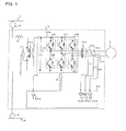
- the voltage detector 11 is connected between the input-side conductors of the inverter module 13b, at the output side of the first core 10a, i.e., at the inverter module 13b side of the first core 10a; however, as illustrated in FIG. 1 , in an electric power converter according to Embodiment 1 of the present invention, the voltage detector 11 is connected between the input-side conductors of the inverter module 13a, at the input side of the first core 10a, i.e., at a place opposite to the inverter module 13a with respect to the first core 10a.
- the first core 10a has an impedance only against a common-mode noise current; therefore, even though the voltage detector 11 is connected between the input-side conductors of the inverter module 13a, at the input side of the first core 10a, i.e., at a place opposite to the inverter module 13a with respect to the first core 10a, the voltage across the capacitor 12 can be detected.
- the current detectors 19a to 19c are disposed inside the case of the inverter module 13b in such a way as to be on the output-side conductors of the inverter module 13b, at the input side of the second core 10b, i.e., at the inverter module 13b side of the second core 10b; however, in an electric power converter according to Embodiment 1 of the present invention, the current detectors 19a to 19c are provided on the output-side conductors of the inverter module 13a at the output side of the second core 10b, i.e., at a place opposite to the inverter module 13a with respect to the second core 10b.
- the current detectors 19a to 19c are disposed outside the inverter module 13a.
- the switching devices SU to SZ in Embodiment 1 are formed of an intelligent power module (referred to an TPM, hereinafter) or a power module integrated with a gate driver having an excessive-current protection function.
- TPM intelligent power module
- An IPM or a power module integrated with a gate driver having an excessive-current protection function has a function of detecting an excessive current due to short-circuiting or a short-to-ground fault of the output conductor thereof and automatically turning off switching operation; therefore, it is not required to detect the excessive current through the current sensors 19a to 19c and turn off the switching operation by the intermediary of the control unit 20, whereby protective operation against the excessive current can rapidly and securely be performed.
- the current sensors 19a to 19c are provided at the output side, (the motor side) of the second core 10b, which is away from the switching devices SU to SZ, it is made possible to protect the switching devices SU to SZ, even though there occurs short-circuiting or a short-to-ground fault of a wiring conductor between the switching devices SU to SZ and the current sensors 19a to 19c.
- the switching devices SU to SZ themselves have an excessive-current protection function; thus, it is made possible to turn off the switching devices SU to SZ so as to avoid the breakage of the electric power converter, even in the case where there occurs short-circuiting or a short-to-ground fault of a wiring conductor between the switching devices SU to SZ and the current sensors 19a to 19c.
- FIG. 2 is a block diagram illustrating an electric power converter according to Embodiment 2 of the present invention.
- the discharging resistor 30 and the discharging device 31 are connected in series and configure an overvoltage-suppression discharging circuit.
- the overvoltage-suppression discharging circuit is connected in parallel with the capacitor 12.
- the voltage detector 11 is connected across the discharging device 31.
- the voltage detector 11 is disposed at the output side of the first core 10a; however, as illustrated in FIG. 2 , in an electric power converter according to Embodiment 2 of the present invention, the voltage detector 11 is disposed at the input side of the first core 10a.
- the first core 10a has an impedance only against a common-mode noise current; therefore, even though disposed at the input side of the first core 10a, the voltage detector 11 can detect the voltage across the capacitor 12.
- the current detectors 19a to 19c are disposed at the input side of the second core 10b and inside the case of the inverter module 13b; however, in the electric power converter according to Embodiment 2 of the present invention, the current detectors 19a to 19c are disposed at the output side of the second core 10b and outside the inverter module 13a.
- Other configurations are the same as those in Embodiment 1.
- FIG. 3 is an explanatory diagram illustrating an equivalent circuit for a common-mode noise current in an electric power converter according to any one of Embodiments 1 and 2 of the present invention.
- the equivalent circuit illustrated in FIG. 3 is represented in a simplified manner, without impairing the physical significance.
- VN denotes a common-mode noise voltage generated by a voltage change due to the switching operations of the switching devices SU to SZ; as the paths of a common-mode noise current generated by the common-mode noise voltage VN, four paths A1, A3, B1, and B3 are conceivable.
- the path A3 is formed of a series circuit including an impedance Z1A between the switching devices SU to SZ and the first core 10a, an impedance Z2A of the first core 10a, an impedance Z5A of the voltage detector 11, an impedance Z6A of a circuit that starts from the voltage detector 11 and leads to the control unit 20 via the insulated amplifier 22a, and an impedance Z7A of a circuit that starts from the control unit 20 and returns to the source of common-mode noise via the case of the electric power converter 6.
- the path B3 is formed of a series circuit including an impedance Z1B between the switching devices SU to SZ and the second core 10b, an impedance Z2B of the second core 10b, an impedance Z5B of the current detectors 19a to 19c, an impedance Z6B of a circuit that starts from the current detectors 19a to 19c and leads to the control unit 20 via the insulated amplifiers 22b to 22d, and an impedance Z7B of a circuit that starts from the control unit 20 and returns to the source of common-mode noise via the case of the electric power converter 6.
- the impedance Z4A of the circuit between the switching devices SU to SZ and the voltage detector 11 becomes the impedance Z1A of the circuit between the switching devices SU to SZ and the first core 10a (Z1A > Z4A)
- the impedance Z4B of the circuit between the switching devices SU to SZ and the current detectors 19a to 19c becomes the impedance Z1B of the circuit between the switching devices SU to SZ and the second core 10b (Z1B > Z4B)
- the impedance Z2A of the first core 10a and the impedance Z2B of the second core 10b are increased.
- the first and second cores 10a and 10b which are originally provided for suppressing a common-mode noise current that flows toward the outside of the electric power converter 6, can also suppress a common-mode noise current that flows to the control unit 20.
- the voltage across the capacitor 12 can be detected; in the case where there occurs an abnormality such as short-circuiting or a short-to-ground fault of the conductors as the output lines of the inverter module 13a, it is made possible to maintain an excessive-current protection function of securely detecting the abnormality and interrupting the switching operation; and a common-mode noise current can be suppressed, without enlargement of components, increase in the number of components, and a cost hike being caused, e.g., by providing a noise suppression means in the voltage detector 11 or the current detector 19a to 19c. Therefore, there can be obtained an electric power converter that can ensure stable operation even though a low-voltage-operation microcomputer of these days is utilized.
- Embodiments 1 and 2 are examples of the aspects of the present invention and can be combined with other publicly known technologies; it goes without saying that various features of the present invention can be configured, by modifying, for example, partially omitting the foregoing embodiments, without departing from the scope and spirit of the present invention.
- Embodiments 1 and 2 of the present invention there has been explained an example in which a voltage detector is disposed at the input side of an inverter module, and current detectors are disposed at the output side of the inverter module; however, it goes without saying that the current detectors may be disposed at the input side of the inverter module, and the voltage detector may be disposed at the output side of the inverter module. Moreover, an electric quantity detector may be provided at a place opposite to the inverter module with respect to only one of the first core 10a and the second core 10b. Still moreover, a switching device having no excessive-current protection function may be utilized.
- the present invention may be applied to an electric power converter configured in such a way that AC power is supplied from a power collector, the AC power is converted into DC power by a converter, and then the DC power is inputted to an inverter module. Additionally, it is also possible to apply the present invention to a so-called auxiliary power source apparatus in which loads such as a vehicle air conditioner and an illumination apparatus are connected to the output terminal of an electric power converter via devices other than a motor, e.g., a transformer and a smoothing circuit, and the electric power converter is operated with a constant voltage and at a constant frequency so that constant-voltage and constant-frequency power is supplied to the loads.
- loads such as a vehicle air conditioner and an illumination apparatus are connected to the output terminal of an electric power converter via devices other than a motor, e.g., a transformer and a smoothing circuit, and the electric power converter is operated with a constant voltage and at a constant frequency so that constant-voltage and constant-frequency power is supplied to the loads.
- An electric power converter according to the present invention can be applied not only to an electric vehicle but also to various related fields such as fields of electric automobiles, elevators, and electric systems.
Landscapes
- Engineering & Computer Science (AREA)
- Power Engineering (AREA)
- Inverter Devices (AREA)
- Power Conversion In General (AREA)
Applications Claiming Priority (1)
| Application Number | Priority Date | Filing Date | Title |
|---|---|---|---|
| PCT/JP2006/312809 WO2008001427A1 (fr) | 2006-06-27 | 2006-06-27 | Convertisseur de courant |
Publications (1)
| Publication Number | Publication Date |
|---|---|
| EP2034601A1 true EP2034601A1 (en) | 2009-03-11 |
Family
ID=38845205
Family Applications (1)
| Application Number | Title | Priority Date | Filing Date |
|---|---|---|---|
| EP06767426A Withdrawn EP2034601A1 (en) | 2006-06-27 | 2006-06-27 | Power converter |
Country Status (6)
| Country | Link |
|---|---|
| US (1) | US20090284199A1 (zh) |
| EP (1) | EP2034601A1 (zh) |
| JP (1) | JPWO2008001427A1 (zh) |
| CN (1) | CN101473519A (zh) |
| CA (1) | CA2655051A1 (zh) |
| WO (1) | WO2008001427A1 (zh) |
Cited By (1)
| Publication number | Priority date | Publication date | Assignee | Title |
|---|---|---|---|---|
| US9252594B2 (en) | 2011-12-28 | 2016-02-02 | Honda Motor Co., Ltd. | Load driving device |
Families Citing this family (15)
| Publication number | Priority date | Publication date | Assignee | Title |
|---|---|---|---|---|
| DE102009008549A1 (de) * | 2009-02-12 | 2010-08-19 | Bombardier Transportation Gmbh | Anordnung zum Betreiben von Verbrauchern in einem Schienenfahrzeug mit elektrischer Energie, wahlweise aus einem Energieversorgungsnetz oder aus einer Motor-Generator-Kombination |
| JP5244653B2 (ja) * | 2009-03-03 | 2013-07-24 | 日立オートモティブシステムズ株式会社 | 電力変換装置 |
| CN201393145Y (zh) * | 2009-04-16 | 2010-01-27 | 中山大洋电机股份有限公司 | 一种电机 |
| JP4930575B2 (ja) * | 2009-11-09 | 2012-05-16 | 三菱電機株式会社 | ノイズ抑制装置、空気調和機 |
| JP5567381B2 (ja) * | 2010-04-27 | 2014-08-06 | 日立オートモティブシステムズ株式会社 | 電力変換装置 |
| JP5456213B2 (ja) * | 2011-09-30 | 2014-03-26 | 三菱電機株式会社 | 電力変換装置 |
| JP5555725B2 (ja) * | 2012-01-13 | 2014-07-23 | 本田技研工業株式会社 | 電気負荷制御装置 |
| JP6182021B2 (ja) * | 2013-08-28 | 2017-08-16 | 株式会社日立製作所 | 電力変換装置 |
| JP2015192489A (ja) * | 2014-03-27 | 2015-11-02 | トヨタ自動車株式会社 | 電源制御装置 |
| JP6177445B2 (ja) * | 2014-08-25 | 2017-08-09 | 三菱電機株式会社 | 電気車制御装置 |
| JP6495666B2 (ja) * | 2015-01-22 | 2019-04-03 | 株式会社東芝 | 車両用電力変換装置 |
| DE102016001196B4 (de) * | 2016-02-03 | 2018-05-30 | Audi Ag | Schaltungsanordnung und Bordnetz für ein Kraftfahrzeug |
| US11296613B2 (en) * | 2017-09-29 | 2022-04-05 | Hitachi Automotive Systems, Ltd. | Power conversion device |
| DE112019002391T5 (de) * | 2018-06-22 | 2021-02-11 | Hitachi Automotive Systems, Ltd. | Leistungsumsetzungsvorrichtung |
| DE102019103404B3 (de) * | 2019-02-12 | 2020-02-27 | Semikron Elektronik Gmbh & Co. Kg | Schaltungseinrichtung mit einem Stromrichter und einer Kodensatorentladungseinrichtung |
Family Cites Families (8)
| Publication number | Priority date | Publication date | Assignee | Title |
|---|---|---|---|---|
| JPH05136592A (ja) * | 1991-11-12 | 1993-06-01 | Fuji Electric Co Ltd | インバータ装置 |
| JPH06315277A (ja) * | 1993-03-04 | 1994-11-08 | Fuji Electric Co Ltd | スイッチング電源の電流検出装置 |
| JPH09289786A (ja) * | 1996-04-23 | 1997-11-04 | Shinko Electric Co Ltd | モータ駆動回路 |
| JP3747858B2 (ja) | 2002-02-01 | 2006-02-22 | 株式会社日立製作所 | 車両用インバータの制御方法およびインバータ制御器 |
| US6717442B2 (en) * | 2002-04-15 | 2004-04-06 | Broadcom Corporation | Dynamic to static converter with noise suppression |
| JP2004187368A (ja) * | 2002-12-02 | 2004-07-02 | Toshiba Corp | 車両用電力変換装置 |
| JP2005033895A (ja) * | 2003-07-10 | 2005-02-03 | Toshiba Corp | 電力変換装置 |
| JP2006033968A (ja) * | 2004-07-14 | 2006-02-02 | Yaskawa Electric Corp | 半導体電力変換装置 |
-
2006
- 2006-06-27 US US12/308,075 patent/US20090284199A1/en not_active Abandoned
- 2006-06-27 JP JP2006552408A patent/JPWO2008001427A1/ja active Pending
- 2006-06-27 CN CNA200680055040XA patent/CN101473519A/zh active Pending
- 2006-06-27 CA CA002655051A patent/CA2655051A1/en not_active Abandoned
- 2006-06-27 WO PCT/JP2006/312809 patent/WO2008001427A1/ja active Application Filing
- 2006-06-27 EP EP06767426A patent/EP2034601A1/en not_active Withdrawn
Non-Patent Citations (1)
| Title |
|---|
| See references of WO2008001427A1 * |
Cited By (1)
| Publication number | Priority date | Publication date | Assignee | Title |
|---|---|---|---|---|
| US9252594B2 (en) | 2011-12-28 | 2016-02-02 | Honda Motor Co., Ltd. | Load driving device |
Also Published As
| Publication number | Publication date |
|---|---|
| US20090284199A1 (en) | 2009-11-19 |
| CA2655051A1 (en) | 2008-01-03 |
| CN101473519A (zh) | 2009-07-01 |
| JPWO2008001427A1 (ja) | 2009-11-19 |
| WO2008001427A1 (fr) | 2008-01-03 |
Similar Documents
| Publication | Publication Date | Title |
|---|---|---|
| EP2034601A1 (en) | Power converter | |
| EP1811645A1 (en) | Power supply circuit protecting method and apparatus for the same | |
| CN109643959B (zh) | 电力变换装置以及逻辑电路 | |
| US9571026B2 (en) | Inverter apparatus | |
| US11183963B2 (en) | Abnormality detection device | |
| US9024564B2 (en) | Drive control device and drive control method | |
| JP6848183B2 (ja) | 電流検出装置および半導体装置 | |
| US20170005570A1 (en) | Power converter | |
| JP4835930B2 (ja) | 地絡検出手段を備えたインバータ装置 | |
| US20060044045A1 (en) | Semiconductor apparatus provided with power switching semiconductor device | |
| CN111527684B (zh) | 驱动电路内置型功率模块 | |
| JP5224128B2 (ja) | 電流検出回路 | |
| KR20160022799A (ko) | 반도체 모듈 | |
| KR101958160B1 (ko) | 전자 제어 장치 및 그 제어 방법 | |
| KR20090005207A (ko) | 전력 변환 장치 | |
| JP2016092927A (ja) | 回転電機制御装置 | |
| JP5724913B2 (ja) | 電力変換装置 | |
| JP2005278296A (ja) | コンデンサ装置およびそれを備えた電源システム | |
| JPH1132426A (ja) | インバータの保護装置 | |
| JP2012032359A (ja) | 配線状態検出回路及び制御装置 | |
| RU2381615C1 (ru) | Преобразователь электроэнергии | |
| CN114121917A (zh) | 半导体模块 | |
| WO2024090232A1 (ja) | 異常検出装置 | |
| JP7384053B2 (ja) | インバータ装置 | |
| WO2023026943A1 (ja) | 電力供給装置 |
Legal Events
| Date | Code | Title | Description |
|---|---|---|---|
| PUAI | Public reference made under article 153(3) epc to a published international application that has entered the european phase |
Free format text: ORIGINAL CODE: 0009012 |
|
| 17P | Request for examination filed |
Effective date: 20081125 |
|
| AK | Designated contracting states |
Kind code of ref document: A1 Designated state(s): AT BE BG CH CY CZ DE DK EE ES FI FR GB GR HU IE IS IT LI LT LU LV MC NL PL PT RO SE SI SK TR |
|
| AX | Request for extension of the european patent |
Extension state: AL BA HR MK RS |
|
| STAA | Information on the status of an ep patent application or granted ep patent |
Free format text: STATUS: THE APPLICATION HAS BEEN WITHDRAWN |
|
| 18W | Application withdrawn |
Effective date: 20091001 |