EP2023409A1 - Module électroluminescent à semi-conducteur, dispositif, et son procédé de fabrication - Google Patents
Module électroluminescent à semi-conducteur, dispositif, et son procédé de fabrication Download PDFInfo
- Publication number
- EP2023409A1 EP2023409A1 EP07742670A EP07742670A EP2023409A1 EP 2023409 A1 EP2023409 A1 EP 2023409A1 EP 07742670 A EP07742670 A EP 07742670A EP 07742670 A EP07742670 A EP 07742670A EP 2023409 A1 EP2023409 A1 EP 2023409A1
- Authority
- EP
- European Patent Office
- Prior art keywords
- light emitting
- semiconductor light
- heat dissipation
- emitting elements
- emitting module
- Prior art date
- Legal status (The legal status is an assumption and is not a legal conclusion. Google has not performed a legal analysis and makes no representation as to the accuracy of the status listed.)
- Granted
Links
Images


Classifications
-
- F—MECHANICAL ENGINEERING; LIGHTING; HEATING; WEAPONS; BLASTING
- F21—LIGHTING
- F21V—FUNCTIONAL FEATURES OR DETAILS OF LIGHTING DEVICES OR SYSTEMS THEREOF; STRUCTURAL COMBINATIONS OF LIGHTING DEVICES WITH OTHER ARTICLES, NOT OTHERWISE PROVIDED FOR
- F21V29/00—Protecting lighting devices from thermal damage; Cooling or heating arrangements specially adapted for lighting devices or systems
-
- F—MECHANICAL ENGINEERING; LIGHTING; HEATING; WEAPONS; BLASTING
- F21—LIGHTING
- F21K—NON-ELECTRIC LIGHT SOURCES USING LUMINESCENCE; LIGHT SOURCES USING ELECTROCHEMILUMINESCENCE; LIGHT SOURCES USING CHARGES OF COMBUSTIBLE MATERIAL; LIGHT SOURCES USING SEMICONDUCTOR DEVICES AS LIGHT-GENERATING ELEMENTS; LIGHT SOURCES NOT OTHERWISE PROVIDED FOR
- F21K9/00—Light sources using semiconductor devices as light-generating elements, e.g. using light-emitting diodes [LED] or lasers
-
- F—MECHANICAL ENGINEERING; LIGHTING; HEATING; WEAPONS; BLASTING
- F21—LIGHTING
- F21V—FUNCTIONAL FEATURES OR DETAILS OF LIGHTING DEVICES OR SYSTEMS THEREOF; STRUCTURAL COMBINATIONS OF LIGHTING DEVICES WITH OTHER ARTICLES, NOT OTHERWISE PROVIDED FOR
- F21V29/00—Protecting lighting devices from thermal damage; Cooling or heating arrangements specially adapted for lighting devices or systems
- F21V29/50—Cooling arrangements
- F21V29/70—Cooling arrangements characterised by passive heat-dissipating elements, e.g. heat-sinks
- F21V29/74—Cooling arrangements characterised by passive heat-dissipating elements, e.g. heat-sinks with fins or blades
-
- F—MECHANICAL ENGINEERING; LIGHTING; HEATING; WEAPONS; BLASTING
- F21—LIGHTING
- F21V—FUNCTIONAL FEATURES OR DETAILS OF LIGHTING DEVICES OR SYSTEMS THEREOF; STRUCTURAL COMBINATIONS OF LIGHTING DEVICES WITH OTHER ARTICLES, NOT OTHERWISE PROVIDED FOR
- F21V29/00—Protecting lighting devices from thermal damage; Cooling or heating arrangements specially adapted for lighting devices or systems
- F21V29/50—Cooling arrangements
- F21V29/70—Cooling arrangements characterised by passive heat-dissipating elements, e.g. heat-sinks
- F21V29/83—Cooling arrangements characterised by passive heat-dissipating elements, e.g. heat-sinks the elements having apertures, ducts or channels, e.g. heat radiation holes
-
- F—MECHANICAL ENGINEERING; LIGHTING; HEATING; WEAPONS; BLASTING
- F21—LIGHTING
- F21S—NON-PORTABLE LIGHTING DEVICES; SYSTEMS THEREOF; VEHICLE LIGHTING DEVICES SPECIALLY ADAPTED FOR VEHICLE EXTERIORS
- F21S2/00—Systems of lighting devices, not provided for in main groups F21S4/00 - F21S10/00 or F21S19/00, e.g. of modular construction
- F21S2/005—Systems of lighting devices, not provided for in main groups F21S4/00 - F21S10/00 or F21S19/00, e.g. of modular construction of modular construction
-
- F—MECHANICAL ENGINEERING; LIGHTING; HEATING; WEAPONS; BLASTING
- F21—LIGHTING
- F21Y—INDEXING SCHEME ASSOCIATED WITH SUBCLASSES F21K, F21L, F21S and F21V, RELATING TO THE FORM OR THE KIND OF THE LIGHT SOURCES OR OF THE COLOUR OF THE LIGHT EMITTED
- F21Y2115/00—Light-generating elements of semiconductor light sources
- F21Y2115/10—Light-emitting diodes [LED]
-
- H—ELECTRICITY
- H01—ELECTRIC ELEMENTS
- H01L—SEMICONDUCTOR DEVICES NOT COVERED BY CLASS H10
- H01L2224/00—Indexing scheme for arrangements for connecting or disconnecting semiconductor or solid-state bodies and methods related thereto as covered by H01L24/00
- H01L2224/01—Means for bonding being attached to, or being formed on, the surface to be connected, e.g. chip-to-package, die-attach, "first-level" interconnects; Manufacturing methods related thereto
- H01L2224/42—Wire connectors; Manufacturing methods related thereto
- H01L2224/47—Structure, shape, material or disposition of the wire connectors after the connecting process
- H01L2224/48—Structure, shape, material or disposition of the wire connectors after the connecting process of an individual wire connector
- H01L2224/4805—Shape
- H01L2224/4809—Loop shape
- H01L2224/48091—Arched
-
- H—ELECTRICITY
- H01—ELECTRIC ELEMENTS
- H01L—SEMICONDUCTOR DEVICES NOT COVERED BY CLASS H10
- H01L2924/00—Indexing scheme for arrangements or methods for connecting or disconnecting semiconductor or solid-state bodies as covered by H01L24/00
- H01L2924/01—Chemical elements
- H01L2924/01078—Platinum [Pt]
-
- H—ELECTRICITY
- H01—ELECTRIC ELEMENTS
- H01L—SEMICONDUCTOR DEVICES NOT COVERED BY CLASS H10
- H01L2924/00—Indexing scheme for arrangements or methods for connecting or disconnecting semiconductor or solid-state bodies as covered by H01L24/00
- H01L2924/01—Chemical elements
- H01L2924/01087—Francium [Fr]
-
- H—ELECTRICITY
- H01—ELECTRIC ELEMENTS
- H01L—SEMICONDUCTOR DEVICES NOT COVERED BY CLASS H10
- H01L33/00—Semiconductor devices with at least one potential-jump barrier or surface barrier specially adapted for light emission; Processes or apparatus specially adapted for the manufacture or treatment thereof or of parts thereof; Details thereof
- H01L33/48—Semiconductor devices with at least one potential-jump barrier or surface barrier specially adapted for light emission; Processes or apparatus specially adapted for the manufacture or treatment thereof or of parts thereof; Details thereof characterised by the semiconductor body packages
- H01L33/62—Arrangements for conducting electric current to or from the semiconductor body, e.g. lead-frames, wire-bonds or solder balls
-
- H—ELECTRICITY
- H01—ELECTRIC ELEMENTS
- H01L—SEMICONDUCTOR DEVICES NOT COVERED BY CLASS H10
- H01L33/00—Semiconductor devices with at least one potential-jump barrier or surface barrier specially adapted for light emission; Processes or apparatus specially adapted for the manufacture or treatment thereof or of parts thereof; Details thereof
- H01L33/48—Semiconductor devices with at least one potential-jump barrier or surface barrier specially adapted for light emission; Processes or apparatus specially adapted for the manufacture or treatment thereof or of parts thereof; Details thereof characterised by the semiconductor body packages
- H01L33/64—Heat extraction or cooling elements
- H01L33/642—Heat extraction or cooling elements characterized by the shape
Definitions
- LEDs light emitting diodes
- one or more sets of power supply terminals are included in one or both of any positions of the heat dissipation block which becomes one electrode to supply power to the semiconductor light emitting elements and the power distribution film which becomes the other electrode to supply the power.
- a semiconductor light emitting device including: a semiconductor light emitting module including semiconductor light emitting elements, a heat dissipation block which becomes one electrode to supply power to the semiconductor light emitting elements disposed in contact with a surface of the heat dissipation block, an insulating film which covers any portion of the surface of the heat dissipation block except for the semiconductor light emitting elements and neighborhoods thereof, and a power distribution film which is disposed in contact with any surface of the insulating film, is electrically connected to the semiconductor light emitting elements, and becomes the other electrode to supply power; and a housing including a power source to supply power to the semiconductor light emitting elements, and a supporting means to support the semiconductor light emitting module.
- a method of manufacturing a semiconductor light emitting module including the steps of: disposing semiconductor light emitting elements in contact with a surface of a heat dissipation block which becomes one electrode to supply power to the semiconductor light emitting elements; covering any portion of the surface of the heat dissipation block with an insulating film except for the semiconductor light emitting elements and neighborhoods thereof; and disposing a power distribution film in contact with any surface of the insulating film, the power distribution film being electrically connected to the semiconductor light emitting elements and being the other electrode to supply the power.
- the method further includes the step of manufacturing the heat dissipation block by cutting erecting a portion of a metal plate.
- the place of the power distribution film 104 where the conductive wires 112 are connected to the power distribution film 104 is subjected to surface plating known in the art.
- the light emitted from the semiconductor light emitting elements 111 may be concentrated by covering the semiconductor light emitting module 101 with a case 202 in actuality, as shown in Fig. 2 .
- the case 202 may be made of material such as polycarbonate, acryl, or glass, but without being limited thereto, may be made of any material known in the art and may have any shape.
- the above-mentioned resin or the like may not be sealed.
- the power distribution film is formed by pressing a metal plate in the shape shown in Fig. 3A .
- holes are formed in the power distribution film as the insulating film, and a terminal to be connected to a power source is formed in the power distribution film.
- penetration holes corresponding to the top side of the semiconductor light emitting elements may have a concave mirror-like shape as shown in Fig. 7 , thereby concentrating light and thus increasing luminance.
- material 701 such as resin or the like, known in the art is sealed into the penetration holes exposed to the outside in order protect the elements, as shown in Fig. 7 .
- the material 701 used for sealing may be silicon, epoxy or the like.
- a connection unit using a plurality of semiconductor light emitting modules may be configured by providing the modules with connections 601 interconnecting the modules, as shown in Fig. 6 .
- a connection unit using a plurality of semiconductor light emitting modules may be configured by providing the modules with connections 601 interconnecting the modules, as shown in Fig. 6 .
- modules manufactured according the following manufacturing method examples may be interconnected in the same way.
- Figs. 4A to 4C are views for explaining a method of manufacturing a semiconductor light emitting module using heat dissipation blocks prepared by metal plate bending or extrusion molding according to this embodiment.
- Fig. 4C shows heat dissipation fins 113 having a waveform-like shape by bending or extrusion molding.
- the heat dissipation fins 113 are arranged in parallel to each other, when the semiconductor light emitting module is disposed in such a manner that the heat dissipation fins 113 are vertically placed, air heated by the heat dissipation is raised along grooves of the fins, and thus convection of air having lower temperature, which is supplied from a lower side, occurs naturally, which results in promotion of heat dissipation.
- the effect obtained when the semiconductor light emitting elements are disposed to face downward is similar to that described above.
- the insulating film is formed by applying or coating an adhesive or the like having an insulation property on portions except for the semiconductor light emitting elements 111 on the top side of the heat dissipation blocks according to any method known in the art, as shown in Fig. 4B .
- the insulating film is prevented from being formed in portions corresponding to penetration holes and vents of the heat dissipation blocks.
- Figs. 5A to 5C are views for explaining a method of manufacturing a semiconductor light emitting module using heat dissipation blocks prepared by extrusion molding according to this embodiment.
- Fig. 5C shows heat dissipation blocks formed by extrusion molding in a normal direction of a loading surface of semiconductor light emitting elements. With such a shape, a process of forming vents after forming the blocks may be omitted.
- the effect obtained when the semiconductor light emitting elements are disposed to face downward is similar to that described above.
- Figs. 16A to 16D are views for explaining a method of manufacturing a semiconductor light emitting module using heat dissipation blocks prepared by cutting and erecting some of a metal plate according to this embodiment.
- Fig. 16C shows heat dissipation blocks formed by cutting and erecting some of a metal plate.
- the holes intended to generate the above-shown and described air current may not be required to be provided depending on the specification of a product, particularly a product including one semiconductor light emitting module or a plurality of semiconductor light emitting modules arranged in a line, or attachment sites or use environments of semiconductor light emitting modules, but the heat dissipation blocks may have a U-like or L-like section for achieving better effects.
- a terminal connected to a power source like the terminal formed in the above-described power distribution film.
- the power distribution film is formed using a metal plate having a shape shown in Fig. 16A .
- a portion exhibiting the function of the above-described reflection plate and being shown in Fig. 16D is formed by preparing individual reflecting parts.
- Material of these reflecting parts may be metal, resin or the like and may be manufactured by any appropriate method known in the art.
- the reflecting parts are prepared using metal and are pressed into the power distribution film formed by the metal plate for both of maintenance and conduction.
- the power distribution film is connected to the semiconductor light emitting elements by means of the conductive wires.
- any appropriate method known in the art such as using resin as material and plating a surface of the resin with conductive material.
- a conductive adhesive or the like may be used to fix the power distribution film and the reflecting parts.
- the semiconductor light emitting module 101 is not necessarily covered with an integrated case, but individual semiconductor light emitting elements 111 may be covered with respective cases, as described in this manufacturing method example.
- Penetration holes and vents of the power distribution film are formed in the same places and with the same shape as in the above manufacturing method example 1.
- the power distribution film is laminated like the above-described insulating film.
- the member 701 such as resin or the like is sealed in a way similar to that described above.
- the four kinds of manufacturing method examples have been described.
- the insulating film is formed in appropriate places of a conductive portion except for the connections of the semiconductor light emitting elements and a supply portion of the power source according to any method known in the art, and one of the manufacturing method examples is selected depending on use purpose and a packaging method of the product.
- Figs. 8A to 8D are conceptual views showing a structure of a semiconductor light emitting module manufactured according to another embodiment of the present invention.
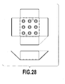
- the semiconductor light emitting elements 111 are placed on a hollow cylindrical heat dissipation block and a semiconductor light emitting module is manufactured as in the above-described manufacturing method examples.
- the semiconductor light emitting elements are placed on a doughnut-like portion on the cylindrical heat dissipation block, the semiconductor light emitting elements may be placed without forming such a doughnut-like portion if the cylindrical heat dissipation block is sufficiently thick.
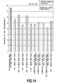
- Fig. 10 is a view showing feature of heat dissipation in case of use of a conventional semiconductor light emitting module
- Fig. 11 is a view showing feature of heat dissipation of a semiconductor light emitting module according to an embodiment of the present invention.
- the semiconductor light emitting module of the present invention used for measurement is that manufactured according to the manufacturing method example 1 of the first embodiment, and the measurement is made for the semiconductor light emitting module installed downward for ceiling illumination in Figs. 10 and 11 .
- Figs. 12 and 13 are views showing a thermal characteristic calculated in case of emission of light from a conventional semiconductor light emitting element and in case of emission of light from a semiconductor light emitting module manufactured according to the manufacturing method example 1 of the first embodiment, respectively.
- Fig. 12 shows the thermal characteristic when the semiconductor light emitting module is used for ceiling illumination
- Fig. 13 shows the thermal characteristic when the semiconductor light emitting module is used for wall illumination.
- the semiconductor light emitting module of the present invention for both of ceiling and wall can suppress increase of temperature even when an electrical input (input power) to the semiconductor light emitting module is increased.
- the semiconductor light emitting module of the present invention is directly formed on the heat dissipation blocks, it is possible to easily manufacture the module, reduce product costs and achieve high luminance emission by large current with highly-efficient heat dissipation.
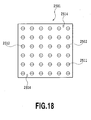
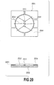
- FIG. 18 is a front view showing a structure of a semiconductor light emitting module according to this embodiment
- Fig. 19 is a front view and a sectional view showing enlargement of a portion of the structure.
- a semiconductor light emitting module 2501 of this embodiment includes a high-reflection plate 2502 having functions of heat dissipation and light reflection, an insulating film 2503 covering the high-reflection plate 2502, and a power distribution film 2504 laminated via the insulating film 2503 and acting as an electrode.
- One or more semiconductor light emitting elements 2511 which are actually conducted to emit light are connected to the power distribution film 2504 via conductive wires 2512.
- the high-reflection plate 2502 has 95% or more, preferably 98% or more, of the overall reflectivity for sufficient emission of light.
- the high-reflection plate 2502 may be mounted by forming an adhesive layer on an aluminum base, forming a pure aluminum layer or a pure silver layer thereon, and forming a reflection-enhancing film thereon by depositing titanium oxide or silicon oxide. This reflection-enhancing film allows reduction of deterioration due to oxidation by inner pure aluminum or pure silver, thereby maintaining reflectivity longer than initial reflectivity, which may result in stabilization of product quality.
- the high-reflection plate 2502 may be manufactured by forming the reflection-enhancing film on metal finished into a desired shape by, for example, pressing or the like by depositing titanium oxide or silicon oxide on the above-described adhesive layer and pure aluminum layer or pure silver layer, or may be manufactured by forming the reflection-enhancing film on plate-like or coil-like metal and then finishing the film into a desired shape by pressing or the like.
- An example of this embodiment uses MIRO2-SILVER and MIRO2 available from ALANOD Company, which have 98% and 95% of the overall reflectivity, respectively.
- the high-reflection plate used in the present invention may be any appropriate reflection plate known in the art as long as it can achieve the object of the present invention, instead of the products available from ALANOD Company.
- the high-reflection plate 2502 may be employed as one electrode.
- the insulating film 2503 provides electrical isolation between at least the high-reflection plate 2502 and the power distribution film 2504, and may have any appropriate shape known in the art as long as it can include holes through which light emitted from the semiconductor light emitting elements 2511 is transmitted to the outside.
- the insulating film 2503 may be formed by inserting a substrate made of FR-4, polyimide or the like between the power distribution film 2504 and the high-reflection plate 2502 or by forming an insulating layer by adhering the power distribution film 2504 to the high-reflection plate 2502 by means of an insulating adhesive.
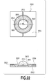
- Fig. 25B is a view for explaining an effect which does not exist in the prior art in case where the method of this example is employed.
- Fig. 25A showing a formation structure of a conventional general fluorescent substance or diffusion agent
- the structure of this example shown in Fig. 25B can make the fluorescent substance or diffusion agent uniform, it is possible to further reduce loss of light as compared to the conventional structure.
- Fig. 25A it is difficult to obtain uniform white or diffused light since the content of fluorescent substance or diffusion agent is different depending direction of light emitted from the semiconductor light emitting elements 2511.
- a circular concave groove 2801 on the high-reflection plate 2502 around the semiconductor light emitting element 2511 and forming the dome 2802 thereon using a surface tension of the resin a uniform resin layer is formed around the semiconductor light emitting element 2511 such that light passes through the resin by the same distance.
- the concave groove 2801 may have any size, position and shape as long as it can use a surface tension of the resin and may be formed by, for example, pressing or any appropriate method known in the art.
- the semiconductor light emitting module includes the heat dissipation blocks which become one electrode to supply power to semiconductor light emitting elements arranged in contact with surfaces of the heat dissipation blocks, the insulating film which covers any portions of the surfaces of the heat dissipation blocks except for the semiconductor light emitting elements and the neighborhood thereof, and the power distribution film which is disposed in contact with any surface of the insulating film, is electrically connected to the semiconductor light emitting elements, and becomes the other electrode to supply power, it is possible to provide a semiconductor light emitting module and device and a method of manufacturing the same, which are capable of preventing luminance characteristics from being deteriorated even when large current is flown, thereby achieving high luminance, by suppressing temperature from being increased by dissipating heat, which is generated in the semiconductor light emitting elements, with high efficiency. In addition, it is possible to maintain higher reflectivity to obtain uniform white light and increase emission efficiency of light to achieve light emission with high luminance.
Applications Claiming Priority (4)
| Application Number | Priority Date | Filing Date | Title |
|---|---|---|---|
| JP2006126918 | 2006-04-28 | ||
| JP2006280448 | 2006-10-13 | ||
| JP2007059186 | 2007-02-07 | ||
| PCT/JP2007/059235 WO2007126074A1 (fr) | 2006-04-28 | 2007-04-27 | Module électroluminescent à semi-conducteur, dispositif, et son procédé de fabrication |
Publications (4)
| Publication Number | Publication Date |
|---|---|
| EP2023409A1 true EP2023409A1 (fr) | 2009-02-11 |
| EP2023409A4 EP2023409A4 (fr) | 2012-03-07 |
| EP2023409B1 EP2023409B1 (fr) | 2017-12-20 |
| EP2023409B8 EP2023409B8 (fr) | 2018-06-27 |
Family
ID=38655594
Family Applications (1)
| Application Number | Title | Priority Date | Filing Date |
|---|---|---|---|
| EP07742670.8A Not-in-force EP2023409B8 (fr) | 2006-04-28 | 2007-04-27 | Module electroluminescent a semi-conducteur et dispositif et son procede de fabrication |
Country Status (5)
| Country | Link |
|---|---|
| EP (1) | EP2023409B8 (fr) |
| JP (2) | JPWO2007126074A1 (fr) |
| KR (1) | KR101136442B1 (fr) |
| CN (1) | CN101432899B (fr) |
| WO (1) | WO2007126074A1 (fr) |
Cited By (6)
| Publication number | Priority date | Publication date | Assignee | Title |
|---|---|---|---|---|
| WO2011029724A1 (fr) * | 2009-09-14 | 2011-03-17 | Osram Gesellschaft mit beschränkter Haftung | Dispositif d'éclairage et procédé pour fabriquer un corps refroidisseur du dispositif d'éclairage et le dispositif d'éclairage |
| WO2011051310A1 (fr) * | 2009-10-27 | 2011-05-05 | Ceramtec Gmbh | Matrice de supports en céramique modulables munis de diodes électroluminescentes |
| EP2738456A1 (fr) * | 2012-11-28 | 2014-06-04 | Chao-Chin Yeh | Combinaison d'une lampe LED et système de refroidissement |
| US9022613B2 (en) | 2008-03-26 | 2015-05-05 | Shimane Prefectural Government | Semiconductor light emitting device comprising cut-and-bent portions |
| US9343643B2 (en) | 2013-04-12 | 2016-05-17 | Nichia Corporation | Light emitting device |
| US10084122B2 (en) | 2014-07-17 | 2018-09-25 | Citizen Electronics Co., Ltd. | Light-emitting apparatus and method of manufacturing the same |
Families Citing this family (8)
| Publication number | Priority date | Publication date | Assignee | Title |
|---|---|---|---|---|
| TWI306674B (en) * | 2006-04-28 | 2009-02-21 | Delta Electronics Inc | Light emitting apparatus |
| US7825384B1 (en) | 2007-10-15 | 2010-11-02 | Positron Corporation | Quantum detector array |
| US8567988B2 (en) * | 2008-09-29 | 2013-10-29 | Bridgelux, Inc. | Efficient LED array |
| KR100959665B1 (ko) * | 2009-07-23 | 2010-05-26 | 세기이테크 주식회사 | 파워엘이디 램프 |
| CN103874883A (zh) * | 2011-10-11 | 2014-06-18 | 普司科Led股份有限公司 | 光学半导体照明设备 |
| KR101149201B1 (ko) * | 2011-12-20 | 2012-05-25 | 한윤희 | 광고용 엘이디 모듈 및 광고용 엘이디 모듈 제조방법 |
| CN103367611B (zh) | 2012-03-28 | 2017-08-08 | 日亚化学工业株式会社 | 波长变换用无机成型体及其制造方法以及发光装置 |
| JP7177327B2 (ja) * | 2017-04-06 | 2022-11-24 | 日亜化学工業株式会社 | 発光装置 |
Citations (5)
| Publication number | Priority date | Publication date | Assignee | Title |
|---|---|---|---|---|
| US20030076033A1 (en) * | 2001-10-19 | 2003-04-24 | Jiahn-Chang Wu | Ventilated light emitting diode matrix panel |
| EP1467414A1 (fr) * | 2001-12-29 | 2004-10-13 | Hangzhou Fuyang Xinying Dianzi Ltd. | Del et lampe a del |
| US20040222433A1 (en) * | 2003-05-05 | 2004-11-11 | Lamina Ceramics | Light emitting diodes packaged for high temperature operation |
| EP1502752A2 (fr) * | 2003-08-01 | 2005-02-02 | Fuji Photo Film Co., Ltd. | Dispositif d'éclairage utilisant des diodes électroluminescents |
| WO2006028073A1 (fr) * | 2004-09-07 | 2006-03-16 | Hitachi Aic Inc. | Dispositif émetteur de lumière de type composant de puce et platine de câblage pour celui-ci |
Family Cites Families (21)
| Publication number | Priority date | Publication date | Assignee | Title |
|---|---|---|---|---|
| JPS63168372A (ja) * | 1987-01-05 | 1988-07-12 | Alps Electric Co Ltd | 発光ダイオ−ドプリントヘツド |
| JPH0644116Y2 (ja) * | 1988-07-05 | 1994-11-14 | 三洋電機株式会社 | 炭化ケイ素発光ダイオード装置 |
| JPH02298084A (ja) * | 1989-05-12 | 1990-12-10 | Matsushita Electric Ind Co Ltd | 発光ダイオード素子の封止方法 |
| US5660461A (en) * | 1994-12-08 | 1997-08-26 | Quantum Devices, Inc. | Arrays of optoelectronic devices and method of making same |
| JP2927279B2 (ja) | 1996-07-29 | 1999-07-28 | 日亜化学工業株式会社 | 発光ダイオード |
| JP3618534B2 (ja) * | 1997-11-28 | 2005-02-09 | 同和鉱業株式会社 | 光通信用ランプ装置とその製造方法 |
| US6335548B1 (en) * | 1999-03-15 | 2002-01-01 | Gentex Corporation | Semiconductor radiation emitter package |
| JP3743186B2 (ja) * | 1998-12-15 | 2006-02-08 | 松下電工株式会社 | 発光ダイオード |
| JP2002093206A (ja) | 2000-09-18 | 2002-03-29 | Stanley Electric Co Ltd | Led信号灯具 |
| JP2002223007A (ja) | 2000-11-22 | 2002-08-09 | Matsushita Electric Ind Co Ltd | 光源ユニット及びこれを用いた半導体発光照明装置 |
| DE20021660U1 (de) * | 2000-12-20 | 2002-05-02 | Alanod Al Veredlung Gmbh | Verbundmaterial |
| JP2004128433A (ja) * | 2002-08-08 | 2004-04-22 | Eru Kogen:Kk | ヒートシンク内蔵ネジ式led電球 |
| JP2004207367A (ja) * | 2002-12-24 | 2004-07-22 | Toyoda Gosei Co Ltd | 発光ダイオード及び発光ダイオード配列板 |
| US6828660B2 (en) * | 2003-01-17 | 2004-12-07 | Texas Instruments Incorporated | Semiconductor device with double nickel-plated leadframe |
| WO2004084319A1 (fr) * | 2003-03-18 | 2004-09-30 | Sumitomo Electric Industries Ltd. | Element de montage pour un element electroluminescent, et dispositif a semi-conducteur utilisant celui-ci |
| JP4289088B2 (ja) * | 2003-08-28 | 2009-07-01 | セイコーエプソン株式会社 | 光源装置 |
| CN2696134Y (zh) * | 2004-05-24 | 2005-04-27 | 葛世潮 | 色温可调的白光发光二极管 |
| JP2005277331A (ja) * | 2004-03-26 | 2005-10-06 | Kyocera Corp | 発光装置および照明装置 |
| JP4127220B2 (ja) * | 2004-02-24 | 2008-07-30 | 松下電工株式会社 | Led実装用プリント基板及びその製造方法 |
| JP4744093B2 (ja) * | 2004-03-23 | 2011-08-10 | ネオプト株式会社 | 照明ユニットおよびそれを用いた照明装置 |
| TW200629596A (en) * | 2004-09-16 | 2006-08-16 | Hitachi Aic Inc | Reflector for led and led device |
-
2007
- 2007-04-27 WO PCT/JP2007/059235 patent/WO2007126074A1/fr active Search and Examination
- 2007-04-27 EP EP07742670.8A patent/EP2023409B8/fr not_active Not-in-force
- 2007-04-27 KR KR1020087029172A patent/KR101136442B1/ko active IP Right Grant
- 2007-04-27 JP JP2008513302A patent/JPWO2007126074A1/ja active Pending
- 2007-04-27 CN CN200780015513.8A patent/CN101432899B/zh not_active Expired - Fee Related
-
2009
- 2009-09-07 JP JP2009206380A patent/JP4802304B2/ja active Active
Patent Citations (5)
| Publication number | Priority date | Publication date | Assignee | Title |
|---|---|---|---|---|
| US20030076033A1 (en) * | 2001-10-19 | 2003-04-24 | Jiahn-Chang Wu | Ventilated light emitting diode matrix panel |
| EP1467414A1 (fr) * | 2001-12-29 | 2004-10-13 | Hangzhou Fuyang Xinying Dianzi Ltd. | Del et lampe a del |
| US20040222433A1 (en) * | 2003-05-05 | 2004-11-11 | Lamina Ceramics | Light emitting diodes packaged for high temperature operation |
| EP1502752A2 (fr) * | 2003-08-01 | 2005-02-02 | Fuji Photo Film Co., Ltd. | Dispositif d'éclairage utilisant des diodes électroluminescents |
| WO2006028073A1 (fr) * | 2004-09-07 | 2006-03-16 | Hitachi Aic Inc. | Dispositif émetteur de lumière de type composant de puce et platine de câblage pour celui-ci |
Non-Patent Citations (1)
| Title |
|---|
| See also references of WO2007126074A1 * |
Cited By (13)
| Publication number | Priority date | Publication date | Assignee | Title |
|---|---|---|---|---|
| US9022613B2 (en) | 2008-03-26 | 2015-05-05 | Shimane Prefectural Government | Semiconductor light emitting device comprising cut-and-bent portions |
| US9484515B2 (en) | 2008-03-26 | 2016-11-01 | S.E.I Inc. | Semiconductor light emitting module comprising an exposed plate surface |
| CN102575813A (zh) * | 2009-09-14 | 2012-07-11 | 欧司朗股份有限公司 | 照明装置和用于制造照明装置的冷却体和照明装置的方法 |
| WO2011029724A1 (fr) * | 2009-09-14 | 2011-03-17 | Osram Gesellschaft mit beschränkter Haftung | Dispositif d'éclairage et procédé pour fabriquer un corps refroidisseur du dispositif d'éclairage et le dispositif d'éclairage |
| US9175841B2 (en) | 2009-09-14 | 2015-11-03 | Osram Gmbh | Lighting device and method for producing a heat sink of the lighting device and the lighting device |
| CN102575813B (zh) * | 2009-09-14 | 2014-11-05 | 欧司朗股份有限公司 | 照明装置和用于制造照明装置的冷却体和照明装置的方法 |
| US8545054B2 (en) | 2009-10-27 | 2013-10-01 | Ceramtec Gmbh | Array of scalable ceramic diode carriers with LEDs |
| RU2563245C2 (ru) * | 2009-10-27 | 2015-09-20 | Керамтек Гмбх | Матрица из масштабируемых керамических носителей диодов со светодиодами |
| WO2011051310A1 (fr) * | 2009-10-27 | 2011-05-05 | Ceramtec Gmbh | Matrice de supports en céramique modulables munis de diodes électroluminescentes |
| EP2738456A1 (fr) * | 2012-11-28 | 2014-06-04 | Chao-Chin Yeh | Combinaison d'une lampe LED et système de refroidissement |
| US9343643B2 (en) | 2013-04-12 | 2016-05-17 | Nichia Corporation | Light emitting device |
| US9484503B2 (en) | 2013-04-12 | 2016-11-01 | Nichia Corporation | Light emitting device |
| US10084122B2 (en) | 2014-07-17 | 2018-09-25 | Citizen Electronics Co., Ltd. | Light-emitting apparatus and method of manufacturing the same |
Also Published As
| Publication number | Publication date |
|---|---|
| KR101136442B1 (ko) | 2012-04-19 |
| KR20090018073A (ko) | 2009-02-19 |
| JPWO2007126074A1 (ja) | 2009-09-10 |
| EP2023409B1 (fr) | 2017-12-20 |
| JP2009290238A (ja) | 2009-12-10 |
| CN101432899B (zh) | 2014-05-28 |
| EP2023409A4 (fr) | 2012-03-07 |
| EP2023409B8 (fr) | 2018-06-27 |
| WO2007126074A1 (fr) | 2007-11-08 |
| CN101432899A (zh) | 2009-05-13 |
| JP4802304B2 (ja) | 2011-10-26 |
Similar Documents
| Publication | Publication Date | Title |
|---|---|---|
| EP2023409B1 (fr) | Module electroluminescent a semi-conducteur et dispositif et son procede de fabrication | |
| KR101182742B1 (ko) | 반도체 발광모듈 및 그 제조방법 | |
| JP2005005740A (ja) | 半導体発光エミッタパッケージ | |
| WO2010073950A1 (fr) | Dispositif électroluminescent, module électroluminescent et procédé de fabrication de dispositif électroluminescent | |
| JP2007294966A (ja) | 多層反射面構造を有するledパッケージ及びその製造方法 | |
| JP4808550B2 (ja) | 発光ダイオード光源装置、照明装置、表示装置及び交通信号機 | |
| JP2004172170A (ja) | 高輝度発光装置及びその製造方法 | |
| JPWO2005043637A1 (ja) | 発光装置 | |
| JP2008027898A (ja) | 線光源用ledモジュール | |
| JP2004363533A (ja) | 発光ダイオード素子の製造方法 | |
| US20110084612A1 (en) | Hybrid chip-on-heatsink device and methods | |
| TW201203636A (en) | Light emitting diode device and lighting device using the same | |
| CN100552992C (zh) | 高功率发光元件封装的工艺 | |
| JP2004342791A (ja) | Ledランプおよびled照明具 | |
| KR100741821B1 (ko) | 발광 다이오드 모듈 | |
| KR101329194B1 (ko) | 광 모듈 및 그 제조 방법 | |
| CN102479911B (zh) | 发光器件封装 | |
| JP2009021384A (ja) | 電子部品及び発光装置 | |
| JP2006344693A (ja) | 発光素子実装用ホーロー基板、発光素子モジュール、照明装置、表示装置及び交通信号機 | |
| JP2007013027A (ja) | 発光素子実装用ホーロー基板、発光素子モジュール、照明装置、表示装置及び交通信号機 | |
| JP5635659B1 (ja) | 面発光体ユニット及びユニット連結具 | |
| JP2000294838A (ja) | チップ型発光ダイオードアレイ | |
| JP2010073724A (ja) | 発光モジュール | |
| JP2007158086A (ja) | Led素子の実装金属基板の形状及びled素子実装基板。 | |
| JP2006156603A (ja) | 発光素子収納用パッケージおよび発光装置ならびに照明装置 |
Legal Events
| Date | Code | Title | Description |
|---|---|---|---|
| PUAI | Public reference made under article 153(3) epc to a published international application that has entered the european phase |
Free format text: ORIGINAL CODE: 0009012 |
|
| 17P | Request for examination filed |
Effective date: 20081126 |
|
| AK | Designated contracting states |
Kind code of ref document: A1 Designated state(s): AT BE BG CH CY CZ DE DK EE ES FI FR GB GR HU IE IS IT LI LT LU LV MC MT NL PL PT RO SE SI SK TR |
|
| AX | Request for extension of the european patent |
Extension state: AL BA HR MK RS |
|
| A4 | Supplementary search report drawn up and despatched |
Effective date: 20120203 |
|
| RIC1 | Information provided on ipc code assigned before grant |
Ipc: F21K 99/00 20100101AFI20120130BHEP Ipc: H01L 33/64 20100101ALN20120130BHEP Ipc: F21S 2/00 20060101ALN20120130BHEP Ipc: H01L 33/62 20100101ALN20120130BHEP |
|
| DAX | Request for extension of the european patent (deleted) | ||
| 17Q | First examination report despatched |
Effective date: 20151012 |
|
| GRAP | Despatch of communication of intention to grant a patent |
Free format text: ORIGINAL CODE: EPIDOSNIGR1 |
|
| RIC1 | Information provided on ipc code assigned before grant |
Ipc: H01L 33/48 20100101ALN20170516BHEP Ipc: H01L 33/60 20100101ALI20170516BHEP Ipc: H01L 25/075 20060101AFI20170516BHEP Ipc: H01L 33/62 20100101ALI20170516BHEP Ipc: F21K 9/00 20160101ALN20170516BHEP |
|
| RIC1 | Information provided on ipc code assigned before grant |
Ipc: H01L 33/62 20100101ALI20170601BHEP Ipc: F21K 9/00 20160101ALN20170601BHEP Ipc: H01L 25/075 20060101AFI20170601BHEP Ipc: H01L 33/60 20100101ALI20170601BHEP Ipc: H01L 33/48 20100101ALN20170601BHEP |
|
| INTG | Intention to grant announced |
Effective date: 20170614 |
|
| RIN1 | Information on inventor provided before grant (corrected) |
Inventor name: FURUTA, TORU Inventor name: UENO, TOSHIYUKI Inventor name: FUKUDA, KENICHI Inventor name: KOMATSUBARA, SATOSHI |
|
| GRAS | Grant fee paid |
Free format text: ORIGINAL CODE: EPIDOSNIGR3 |
|
| GRAJ | Information related to disapproval of communication of intention to grant by the applicant or resumption of examination proceedings by the epo deleted |
Free format text: ORIGINAL CODE: EPIDOSDIGR1 |
|
| GRAL | Information related to payment of fee for publishing/printing deleted |
Free format text: ORIGINAL CODE: EPIDOSDIGR3 |
|
| REG | Reference to a national code |
Ref country code: DE Ref legal event code: R079 Ref document number: 602007053462 Country of ref document: DE Free format text: PREVIOUS MAIN CLASS: H01L0033000000 Ipc: H01L0025075000 |
|
| GRAR | Information related to intention to grant a patent recorded |
Free format text: ORIGINAL CODE: EPIDOSNIGR71 |
|
| GRAA | (expected) grant |
Free format text: ORIGINAL CODE: 0009210 |
|
| INTC | Intention to grant announced (deleted) | ||
| RIC1 | Information provided on ipc code assigned before grant |
Ipc: H01L 33/60 20100101ALI20171106BHEP Ipc: H01L 33/48 20100101ALN20171106BHEP Ipc: F21K 9/00 20160101ALN20171106BHEP Ipc: H01L 25/075 20060101AFI20171106BHEP Ipc: H01L 33/62 20100101ALI20171106BHEP |
|
| AK | Designated contracting states |
Kind code of ref document: B1 Designated state(s): AT BE BG CH CY CZ DE DK EE ES FI FR GB GR HU IE IS IT LI LT LU LV MC MT NL PL PT RO SE SI SK TR |
|
| INTG | Intention to grant announced |
Effective date: 20171114 |
|
| REG | Reference to a national code |
Ref country code: GB Ref legal event code: FG4D |
|
| REG | Reference to a national code |
Ref country code: CH Ref legal event code: EP |
|
| REG | Reference to a national code |
Ref country code: IE Ref legal event code: FG4D |
|
| REG | Reference to a national code |
Ref country code: AT Ref legal event code: REF Ref document number: 957104 Country of ref document: AT Kind code of ref document: T Effective date: 20180115 |
|
| REG | Reference to a national code |
Ref country code: DE Ref legal event code: R096 Ref document number: 602007053462 Country of ref document: DE |
|
| REG | Reference to a national code |
Ref country code: DE Ref legal event code: R081 Ref document number: 602007053462 Country of ref document: DE Owner name: SHIMANE PREFECTURAL GOVERNMENT, MATSUE-SHI, JP Free format text: FORMER OWNERS: SHIMANE ELECTRONIC IMAFUKU WORKS CO., LTD., HAMADA-SHI, SHIMANE, JP; SHIMANE PREFECTURAL GOVERNMENT, MATSUE-SHI, SHIMANE, JP Ref country code: DE Ref legal event code: R081 Ref document number: 602007053462 Country of ref document: DE Owner name: S.E.I. INC., HAMADA-SHI, JP Free format text: FORMER OWNERS: SHIMANE ELECTRONIC IMAFUKU WORKS CO., LTD., HAMADA-SHI, SHIMANE, JP; SHIMANE PREFECTURAL GOVERNMENT, MATSUE-SHI, SHIMANE, JP |
|
| RAP2 | Party data changed (patent owner data changed or rights of a patent transferred) |
Owner name: SHIMANE PREFECTURAL GOVERNMENT Owner name: S.E.I. INC. |
|
| REG | Reference to a national code |
Ref country code: FR Ref legal event code: PLFP Year of fee payment: 12 |
|
| REG | Reference to a national code |
Ref country code: NL Ref legal event code: MP Effective date: 20171220 |
|
| PG25 | Lapsed in a contracting state [announced via postgrant information from national office to epo] |
Ref country code: FI Free format text: LAPSE BECAUSE OF FAILURE TO SUBMIT A TRANSLATION OF THE DESCRIPTION OR TO PAY THE FEE WITHIN THE PRESCRIBED TIME-LIMIT Effective date: 20171220 Ref country code: SE Free format text: LAPSE BECAUSE OF FAILURE TO SUBMIT A TRANSLATION OF THE DESCRIPTION OR TO PAY THE FEE WITHIN THE PRESCRIBED TIME-LIMIT Effective date: 20171220 Ref country code: LT Free format text: LAPSE BECAUSE OF FAILURE TO SUBMIT A TRANSLATION OF THE DESCRIPTION OR TO PAY THE FEE WITHIN THE PRESCRIBED TIME-LIMIT Effective date: 20171220 |
|
| GRAT | Correction requested after decision to grant or after decision to maintain patent in amended form |
Free format text: ORIGINAL CODE: EPIDOSNCDEC |
|
| REG | Reference to a national code |
Ref country code: LT Ref legal event code: MG4D |
|
| REG | Reference to a national code |
Ref country code: AT Ref legal event code: MK05 Ref document number: 957104 Country of ref document: AT Kind code of ref document: T Effective date: 20171220 |
|
| PG25 | Lapsed in a contracting state [announced via postgrant information from national office to epo] |
Ref country code: GR Free format text: LAPSE BECAUSE OF FAILURE TO SUBMIT A TRANSLATION OF THE DESCRIPTION OR TO PAY THE FEE WITHIN THE PRESCRIBED TIME-LIMIT Effective date: 20180321 Ref country code: BG Free format text: LAPSE BECAUSE OF FAILURE TO SUBMIT A TRANSLATION OF THE DESCRIPTION OR TO PAY THE FEE WITHIN THE PRESCRIBED TIME-LIMIT Effective date: 20180320 Ref country code: LV Free format text: LAPSE BECAUSE OF FAILURE TO SUBMIT A TRANSLATION OF THE DESCRIPTION OR TO PAY THE FEE WITHIN THE PRESCRIBED TIME-LIMIT Effective date: 20171220 |
|
| PG25 | Lapsed in a contracting state [announced via postgrant information from national office to epo] |
Ref country code: NL Free format text: LAPSE BECAUSE OF FAILURE TO SUBMIT A TRANSLATION OF THE DESCRIPTION OR TO PAY THE FEE WITHIN THE PRESCRIBED TIME-LIMIT Effective date: 20171220 |
|
| PG25 | Lapsed in a contracting state [announced via postgrant information from national office to epo] |
Ref country code: SK Free format text: LAPSE BECAUSE OF FAILURE TO SUBMIT A TRANSLATION OF THE DESCRIPTION OR TO PAY THE FEE WITHIN THE PRESCRIBED TIME-LIMIT Effective date: 20171220 Ref country code: CZ Free format text: LAPSE BECAUSE OF FAILURE TO SUBMIT A TRANSLATION OF THE DESCRIPTION OR TO PAY THE FEE WITHIN THE PRESCRIBED TIME-LIMIT Effective date: 20171220 Ref country code: ES Free format text: LAPSE BECAUSE OF FAILURE TO SUBMIT A TRANSLATION OF THE DESCRIPTION OR TO PAY THE FEE WITHIN THE PRESCRIBED TIME-LIMIT Effective date: 20171220 Ref country code: EE Free format text: LAPSE BECAUSE OF FAILURE TO SUBMIT A TRANSLATION OF THE DESCRIPTION OR TO PAY THE FEE WITHIN THE PRESCRIBED TIME-LIMIT Effective date: 20171220 Ref country code: CY Free format text: LAPSE BECAUSE OF FAILURE TO SUBMIT A TRANSLATION OF THE DESCRIPTION OR TO PAY THE FEE WITHIN THE PRESCRIBED TIME-LIMIT Effective date: 20171220 |
|
| PG25 | Lapsed in a contracting state [announced via postgrant information from national office to epo] |
Ref country code: RO Free format text: LAPSE BECAUSE OF FAILURE TO SUBMIT A TRANSLATION OF THE DESCRIPTION OR TO PAY THE FEE WITHIN THE PRESCRIBED TIME-LIMIT Effective date: 20171220 Ref country code: IS Free format text: LAPSE BECAUSE OF FAILURE TO SUBMIT A TRANSLATION OF THE DESCRIPTION OR TO PAY THE FEE WITHIN THE PRESCRIBED TIME-LIMIT Effective date: 20180420 Ref country code: PL Free format text: LAPSE BECAUSE OF FAILURE TO SUBMIT A TRANSLATION OF THE DESCRIPTION OR TO PAY THE FEE WITHIN THE PRESCRIBED TIME-LIMIT Effective date: 20171220 Ref country code: AT Free format text: LAPSE BECAUSE OF FAILURE TO SUBMIT A TRANSLATION OF THE DESCRIPTION OR TO PAY THE FEE WITHIN THE PRESCRIBED TIME-LIMIT Effective date: 20171220 |
|
| REG | Reference to a national code |
Ref country code: DE Ref legal event code: R097 Ref document number: 602007053462 Country of ref document: DE |
|
| PLBE | No opposition filed within time limit |
Free format text: ORIGINAL CODE: 0009261 |
|
| STAA | Information on the status of an ep patent application or granted ep patent |
Free format text: STATUS: NO OPPOSITION FILED WITHIN TIME LIMIT |
|
| 26N | No opposition filed |
Effective date: 20180921 |
|
| PG25 | Lapsed in a contracting state [announced via postgrant information from national office to epo] |
Ref country code: MC Free format text: LAPSE BECAUSE OF FAILURE TO SUBMIT A TRANSLATION OF THE DESCRIPTION OR TO PAY THE FEE WITHIN THE PRESCRIBED TIME-LIMIT Effective date: 20171220 Ref country code: DK Free format text: LAPSE BECAUSE OF FAILURE TO SUBMIT A TRANSLATION OF THE DESCRIPTION OR TO PAY THE FEE WITHIN THE PRESCRIBED TIME-LIMIT Effective date: 20171220 |
|
| REG | Reference to a national code |
Ref country code: CH Ref legal event code: PL |
|
| REG | Reference to a national code |
Ref country code: BE Ref legal event code: MM Effective date: 20180430 |
|
| REG | Reference to a national code |
Ref country code: IE Ref legal event code: MM4A |
|
| PG25 | Lapsed in a contracting state [announced via postgrant information from national office to epo] |
Ref country code: LU Free format text: LAPSE BECAUSE OF NON-PAYMENT OF DUE FEES Effective date: 20180427 |
|
| PG25 | Lapsed in a contracting state [announced via postgrant information from national office to epo] |
Ref country code: BE Free format text: LAPSE BECAUSE OF NON-PAYMENT OF DUE FEES Effective date: 20180430 Ref country code: CH Free format text: LAPSE BECAUSE OF NON-PAYMENT OF DUE FEES Effective date: 20180430 Ref country code: LI Free format text: LAPSE BECAUSE OF NON-PAYMENT OF DUE FEES Effective date: 20180430 Ref country code: SI Free format text: LAPSE BECAUSE OF FAILURE TO SUBMIT A TRANSLATION OF THE DESCRIPTION OR TO PAY THE FEE WITHIN THE PRESCRIBED TIME-LIMIT Effective date: 20171220 |
|
| PG25 | Lapsed in a contracting state [announced via postgrant information from national office to epo] |
Ref country code: IE Free format text: LAPSE BECAUSE OF NON-PAYMENT OF DUE FEES Effective date: 20180427 |
|
| PGFP | Annual fee paid to national office [announced via postgrant information from national office to epo] |
Ref country code: DE Payment date: 20190329 Year of fee payment: 13 Ref country code: IT Payment date: 20190419 Year of fee payment: 13 |
|
| PGFP | Annual fee paid to national office [announced via postgrant information from national office to epo] |
Ref country code: FR Payment date: 20190423 Year of fee payment: 13 |
|
| PGFP | Annual fee paid to national office [announced via postgrant information from national office to epo] |
Ref country code: GB Payment date: 20190424 Year of fee payment: 13 |
|
| PG25 | Lapsed in a contracting state [announced via postgrant information from national office to epo] |
Ref country code: MT Free format text: LAPSE BECAUSE OF NON-PAYMENT OF DUE FEES Effective date: 20180427 |
|
| PG25 | Lapsed in a contracting state [announced via postgrant information from national office to epo] |
Ref country code: TR Free format text: LAPSE BECAUSE OF FAILURE TO SUBMIT A TRANSLATION OF THE DESCRIPTION OR TO PAY THE FEE WITHIN THE PRESCRIBED TIME-LIMIT Effective date: 20171220 |
|
| PG25 | Lapsed in a contracting state [announced via postgrant information from national office to epo] |
Ref country code: PT Free format text: LAPSE BECAUSE OF FAILURE TO SUBMIT A TRANSLATION OF THE DESCRIPTION OR TO PAY THE FEE WITHIN THE PRESCRIBED TIME-LIMIT Effective date: 20171220 Ref country code: HU Free format text: LAPSE BECAUSE OF FAILURE TO SUBMIT A TRANSLATION OF THE DESCRIPTION OR TO PAY THE FEE WITHIN THE PRESCRIBED TIME-LIMIT; INVALID AB INITIO Effective date: 20070427 |
|
| REG | Reference to a national code |
Ref country code: DE Ref legal event code: R119 Ref document number: 602007053462 Country of ref document: DE |
|
| PG25 | Lapsed in a contracting state [announced via postgrant information from national office to epo] |
Ref country code: DE Free format text: LAPSE BECAUSE OF NON-PAYMENT OF DUE FEES Effective date: 20201103 Ref country code: FR Free format text: LAPSE BECAUSE OF NON-PAYMENT OF DUE FEES Effective date: 20200430 |
|
| GBPC | Gb: european patent ceased through non-payment of renewal fee |
Effective date: 20200427 |
|
| PG25 | Lapsed in a contracting state [announced via postgrant information from national office to epo] |
Ref country code: GB Free format text: LAPSE BECAUSE OF NON-PAYMENT OF DUE FEES Effective date: 20200427 |
|
| PG25 | Lapsed in a contracting state [announced via postgrant information from national office to epo] |
Ref country code: IT Free format text: LAPSE BECAUSE OF NON-PAYMENT OF DUE FEES Effective date: 20200427 |