EP2023409A1 - Semiconductor light emitting module, device, and its manufacturing method - Google Patents
Semiconductor light emitting module, device, and its manufacturing method Download PDFInfo
- Publication number
- EP2023409A1 EP2023409A1 EP07742670A EP07742670A EP2023409A1 EP 2023409 A1 EP2023409 A1 EP 2023409A1 EP 07742670 A EP07742670 A EP 07742670A EP 07742670 A EP07742670 A EP 07742670A EP 2023409 A1 EP2023409 A1 EP 2023409A1
- Authority
- EP
- European Patent Office
- Prior art keywords
- light emitting
- semiconductor light
- heat dissipation
- emitting elements
- emitting module
- Prior art date
- Legal status (The legal status is an assumption and is not a legal conclusion. Google has not performed a legal analysis and makes no representation as to the accuracy of the status listed.)
- Granted
Links
- 239000004065 semiconductor Substances 0.000 title claims abstract description 250
- 238000004519 manufacturing process Methods 0.000 title claims description 61
- 230000017525 heat dissipation Effects 0.000 claims abstract description 156
- 238000009826 distribution Methods 0.000 claims abstract description 82
- 229910052751 metal Inorganic materials 0.000 claims description 47
- 239000002184 metal Substances 0.000 claims description 47
- 238000000034 method Methods 0.000 claims description 36
- 238000005520 cutting process Methods 0.000 claims description 18
- 238000005286 illumination Methods 0.000 claims description 18
- 238000003825 pressing Methods 0.000 claims description 9
- 238000000151 deposition Methods 0.000 claims description 6
- 239000012141 concentrate Substances 0.000 claims description 5
- 238000009413 insulation Methods 0.000 abstract description 4
- 239000011347 resin Substances 0.000 description 24
- 229920005989 resin Polymers 0.000 description 24
- 230000035515 penetration Effects 0.000 description 20
- 239000000126 substance Substances 0.000 description 19
- 239000000463 material Substances 0.000 description 18
- 230000000694 effects Effects 0.000 description 15
- 238000001125 extrusion Methods 0.000 description 15
- 238000002310 reflectometry Methods 0.000 description 15
- 239000010410 layer Substances 0.000 description 14
- 239000003795 chemical substances by application Substances 0.000 description 13
- 238000009792 diffusion process Methods 0.000 description 13
- 238000007747 plating Methods 0.000 description 13
- 229910052709 silver Inorganic materials 0.000 description 11
- 239000004332 silver Substances 0.000 description 11
- 239000000758 substrate Substances 0.000 description 10
- 229910052782 aluminium Inorganic materials 0.000 description 7
- XAGFODPZIPBFFR-UHFFFAOYSA-N aluminium Chemical compound [Al] XAGFODPZIPBFFR-UHFFFAOYSA-N 0.000 description 7
- 238000005452 bending Methods 0.000 description 7
- BQCADISMDOOEFD-UHFFFAOYSA-N Silver Chemical compound [Ag] BQCADISMDOOEFD-UHFFFAOYSA-N 0.000 description 6
- 239000000853 adhesive Substances 0.000 description 5
- 230000001070 adhesive effect Effects 0.000 description 5
- 230000008859 change Effects 0.000 description 5
- 230000008569 process Effects 0.000 description 5
- 230000005855 radiation Effects 0.000 description 5
- 238000012360 testing method Methods 0.000 description 5
- 239000004642 Polyimide Substances 0.000 description 4
- 238000005259 measurement Methods 0.000 description 4
- 229920001721 polyimide Polymers 0.000 description 4
- XUIMIQQOPSSXEZ-UHFFFAOYSA-N Silicon Chemical compound [Si] XUIMIQQOPSSXEZ-UHFFFAOYSA-N 0.000 description 3
- 230000015572 biosynthetic process Effects 0.000 description 3
- 238000003475 lamination Methods 0.000 description 3
- 229910052710 silicon Inorganic materials 0.000 description 3
- 239000010703 silicon Substances 0.000 description 3
- 238000004088 simulation Methods 0.000 description 3
- 239000004593 Epoxy Substances 0.000 description 2
- 101000990976 Homo sapiens Mitochondrial Rho GTPase 2 Proteins 0.000 description 2
- XEEYBQQBJWHFJM-UHFFFAOYSA-N Iron Chemical compound [Fe] XEEYBQQBJWHFJM-UHFFFAOYSA-N 0.000 description 2
- 102100030325 Mitochondrial Rho GTPase 2 Human genes 0.000 description 2
- VYPSYNLAJGMNEJ-UHFFFAOYSA-N Silicium dioxide Chemical compound O=[Si]=O VYPSYNLAJGMNEJ-UHFFFAOYSA-N 0.000 description 2
- GWEVSGVZZGPLCZ-UHFFFAOYSA-N Titan oxide Chemical compound O=[Ti]=O GWEVSGVZZGPLCZ-UHFFFAOYSA-N 0.000 description 2
- -1 acryl Chemical group 0.000 description 2
- 239000012790 adhesive layer Substances 0.000 description 2
- 238000005530 etching Methods 0.000 description 2
- 239000011521 glass Substances 0.000 description 2
- 238000001746 injection moulding Methods 0.000 description 2
- 238000002955 isolation Methods 0.000 description 2
- 239000004417 polycarbonate Substances 0.000 description 2
- 229920000515 polycarbonate Polymers 0.000 description 2
- 229910052814 silicon oxide Inorganic materials 0.000 description 2
- OGIDPMRJRNCKJF-UHFFFAOYSA-N titanium oxide Inorganic materials [Ti]=O OGIDPMRJRNCKJF-UHFFFAOYSA-N 0.000 description 2
- RYGMFSIKBFXOCR-UHFFFAOYSA-N Copper Chemical compound [Cu] RYGMFSIKBFXOCR-UHFFFAOYSA-N 0.000 description 1
- 239000000956 alloy Substances 0.000 description 1
- 229910045601 alloy Inorganic materials 0.000 description 1
- 239000003575 carbonaceous material Substances 0.000 description 1
- 238000005266 casting Methods 0.000 description 1
- 239000000919 ceramic Substances 0.000 description 1
- 239000011248 coating agent Substances 0.000 description 1
- 238000000576 coating method Methods 0.000 description 1
- 150000001875 compounds Chemical class 0.000 description 1
- 239000004020 conductor Substances 0.000 description 1
- 238000007796 conventional method Methods 0.000 description 1
- 229910052802 copper Inorganic materials 0.000 description 1
- 239000010949 copper Substances 0.000 description 1
- 230000008021 deposition Effects 0.000 description 1
- 230000006866 deterioration Effects 0.000 description 1
- 230000001747 exhibiting effect Effects 0.000 description 1
- 230000004907 flux Effects 0.000 description 1
- 238000005242 forging Methods 0.000 description 1
- 230000020169 heat generation Effects 0.000 description 1
- 230000006872 improvement Effects 0.000 description 1
- 229910052742 iron Inorganic materials 0.000 description 1
- 238000010030 laminating Methods 0.000 description 1
- 238000011068 loading method Methods 0.000 description 1
- 238000012423 maintenance Methods 0.000 description 1
- 238000000465 moulding Methods 0.000 description 1
- 230000003647 oxidation Effects 0.000 description 1
- 238000007254 oxidation reaction Methods 0.000 description 1
- 238000004806 packaging method and process Methods 0.000 description 1
- 239000004033 plastic Substances 0.000 description 1
- 229920003023 plastic Polymers 0.000 description 1
- 238000007639 printing Methods 0.000 description 1
- 230000001737 promoting effect Effects 0.000 description 1
- 230000009467 reduction Effects 0.000 description 1
- 238000007789 sealing Methods 0.000 description 1
- 230000011664 signaling Effects 0.000 description 1
- 230000006641 stabilisation Effects 0.000 description 1
- 238000011105 stabilization Methods 0.000 description 1
- 230000001629 suppression Effects 0.000 description 1
Images


Classifications
-
- F—MECHANICAL ENGINEERING; LIGHTING; HEATING; WEAPONS; BLASTING
- F21—LIGHTING
- F21V—FUNCTIONAL FEATURES OR DETAILS OF LIGHTING DEVICES OR SYSTEMS THEREOF; STRUCTURAL COMBINATIONS OF LIGHTING DEVICES WITH OTHER ARTICLES, NOT OTHERWISE PROVIDED FOR
- F21V29/00—Protecting lighting devices from thermal damage; Cooling or heating arrangements specially adapted for lighting devices or systems
-
- F—MECHANICAL ENGINEERING; LIGHTING; HEATING; WEAPONS; BLASTING
- F21—LIGHTING
- F21K—NON-ELECTRIC LIGHT SOURCES USING LUMINESCENCE; LIGHT SOURCES USING ELECTROCHEMILUMINESCENCE; LIGHT SOURCES USING CHARGES OF COMBUSTIBLE MATERIAL; LIGHT SOURCES USING SEMICONDUCTOR DEVICES AS LIGHT-GENERATING ELEMENTS; LIGHT SOURCES NOT OTHERWISE PROVIDED FOR
- F21K9/00—Light sources using semiconductor devices as light-generating elements, e.g. using light-emitting diodes [LED] or lasers
-
- F—MECHANICAL ENGINEERING; LIGHTING; HEATING; WEAPONS; BLASTING
- F21—LIGHTING
- F21V—FUNCTIONAL FEATURES OR DETAILS OF LIGHTING DEVICES OR SYSTEMS THEREOF; STRUCTURAL COMBINATIONS OF LIGHTING DEVICES WITH OTHER ARTICLES, NOT OTHERWISE PROVIDED FOR
- F21V29/00—Protecting lighting devices from thermal damage; Cooling or heating arrangements specially adapted for lighting devices or systems
- F21V29/50—Cooling arrangements
- F21V29/70—Cooling arrangements characterised by passive heat-dissipating elements, e.g. heat-sinks
- F21V29/74—Cooling arrangements characterised by passive heat-dissipating elements, e.g. heat-sinks with fins or blades
-
- F—MECHANICAL ENGINEERING; LIGHTING; HEATING; WEAPONS; BLASTING
- F21—LIGHTING
- F21V—FUNCTIONAL FEATURES OR DETAILS OF LIGHTING DEVICES OR SYSTEMS THEREOF; STRUCTURAL COMBINATIONS OF LIGHTING DEVICES WITH OTHER ARTICLES, NOT OTHERWISE PROVIDED FOR
- F21V29/00—Protecting lighting devices from thermal damage; Cooling or heating arrangements specially adapted for lighting devices or systems
- F21V29/50—Cooling arrangements
- F21V29/70—Cooling arrangements characterised by passive heat-dissipating elements, e.g. heat-sinks
- F21V29/83—Cooling arrangements characterised by passive heat-dissipating elements, e.g. heat-sinks the elements having apertures, ducts or channels, e.g. heat radiation holes
-
- F—MECHANICAL ENGINEERING; LIGHTING; HEATING; WEAPONS; BLASTING
- F21—LIGHTING
- F21S—NON-PORTABLE LIGHTING DEVICES; SYSTEMS THEREOF; VEHICLE LIGHTING DEVICES SPECIALLY ADAPTED FOR VEHICLE EXTERIORS
- F21S2/00—Systems of lighting devices, not provided for in main groups F21S4/00 - F21S10/00 or F21S19/00, e.g. of modular construction
- F21S2/005—Systems of lighting devices, not provided for in main groups F21S4/00 - F21S10/00 or F21S19/00, e.g. of modular construction of modular construction
-
- F—MECHANICAL ENGINEERING; LIGHTING; HEATING; WEAPONS; BLASTING
- F21—LIGHTING
- F21Y—INDEXING SCHEME ASSOCIATED WITH SUBCLASSES F21K, F21L, F21S and F21V, RELATING TO THE FORM OR THE KIND OF THE LIGHT SOURCES OR OF THE COLOUR OF THE LIGHT EMITTED
- F21Y2115/00—Light-generating elements of semiconductor light sources
- F21Y2115/10—Light-emitting diodes [LED]
-
- H—ELECTRICITY
- H01—ELECTRIC ELEMENTS
- H01L—SEMICONDUCTOR DEVICES NOT COVERED BY CLASS H10
- H01L2224/00—Indexing scheme for arrangements for connecting or disconnecting semiconductor or solid-state bodies and methods related thereto as covered by H01L24/00
- H01L2224/01—Means for bonding being attached to, or being formed on, the surface to be connected, e.g. chip-to-package, die-attach, "first-level" interconnects; Manufacturing methods related thereto
- H01L2224/42—Wire connectors; Manufacturing methods related thereto
- H01L2224/47—Structure, shape, material or disposition of the wire connectors after the connecting process
- H01L2224/48—Structure, shape, material or disposition of the wire connectors after the connecting process of an individual wire connector
- H01L2224/4805—Shape
- H01L2224/4809—Loop shape
- H01L2224/48091—Arched
-
- H—ELECTRICITY
- H01—ELECTRIC ELEMENTS
- H01L—SEMICONDUCTOR DEVICES NOT COVERED BY CLASS H10
- H01L2924/00—Indexing scheme for arrangements or methods for connecting or disconnecting semiconductor or solid-state bodies as covered by H01L24/00
- H01L2924/01—Chemical elements
- H01L2924/01078—Platinum [Pt]
-
- H—ELECTRICITY
- H01—ELECTRIC ELEMENTS
- H01L—SEMICONDUCTOR DEVICES NOT COVERED BY CLASS H10
- H01L2924/00—Indexing scheme for arrangements or methods for connecting or disconnecting semiconductor or solid-state bodies as covered by H01L24/00
- H01L2924/01—Chemical elements
- H01L2924/01087—Francium [Fr]
-
- H—ELECTRICITY
- H01—ELECTRIC ELEMENTS
- H01L—SEMICONDUCTOR DEVICES NOT COVERED BY CLASS H10
- H01L33/00—Semiconductor devices having potential barriers specially adapted for light emission; Processes or apparatus specially adapted for the manufacture or treatment thereof or of parts thereof; Details thereof
- H01L33/48—Semiconductor devices having potential barriers specially adapted for light emission; Processes or apparatus specially adapted for the manufacture or treatment thereof or of parts thereof; Details thereof characterised by the semiconductor body packages
- H01L33/62—Arrangements for conducting electric current to or from the semiconductor body, e.g. lead-frames, wire-bonds or solder balls
-
- H—ELECTRICITY
- H01—ELECTRIC ELEMENTS
- H01L—SEMICONDUCTOR DEVICES NOT COVERED BY CLASS H10
- H01L33/00—Semiconductor devices having potential barriers specially adapted for light emission; Processes or apparatus specially adapted for the manufacture or treatment thereof or of parts thereof; Details thereof
- H01L33/48—Semiconductor devices having potential barriers specially adapted for light emission; Processes or apparatus specially adapted for the manufacture or treatment thereof or of parts thereof; Details thereof characterised by the semiconductor body packages
- H01L33/64—Heat extraction or cooling elements
- H01L33/642—Heat extraction or cooling elements characterized by the shape
Definitions
- LEDs light emitting diodes
- one or more sets of power supply terminals are included in one or both of any positions of the heat dissipation block which becomes one electrode to supply power to the semiconductor light emitting elements and the power distribution film which becomes the other electrode to supply the power.
- a semiconductor light emitting device including: a semiconductor light emitting module including semiconductor light emitting elements, a heat dissipation block which becomes one electrode to supply power to the semiconductor light emitting elements disposed in contact with a surface of the heat dissipation block, an insulating film which covers any portion of the surface of the heat dissipation block except for the semiconductor light emitting elements and neighborhoods thereof, and a power distribution film which is disposed in contact with any surface of the insulating film, is electrically connected to the semiconductor light emitting elements, and becomes the other electrode to supply power; and a housing including a power source to supply power to the semiconductor light emitting elements, and a supporting means to support the semiconductor light emitting module.
- a method of manufacturing a semiconductor light emitting module including the steps of: disposing semiconductor light emitting elements in contact with a surface of a heat dissipation block which becomes one electrode to supply power to the semiconductor light emitting elements; covering any portion of the surface of the heat dissipation block with an insulating film except for the semiconductor light emitting elements and neighborhoods thereof; and disposing a power distribution film in contact with any surface of the insulating film, the power distribution film being electrically connected to the semiconductor light emitting elements and being the other electrode to supply the power.
- the method further includes the step of manufacturing the heat dissipation block by cutting erecting a portion of a metal plate.
- the place of the power distribution film 104 where the conductive wires 112 are connected to the power distribution film 104 is subjected to surface plating known in the art.
- the light emitted from the semiconductor light emitting elements 111 may be concentrated by covering the semiconductor light emitting module 101 with a case 202 in actuality, as shown in Fig. 2 .
- the case 202 may be made of material such as polycarbonate, acryl, or glass, but without being limited thereto, may be made of any material known in the art and may have any shape.
- the above-mentioned resin or the like may not be sealed.
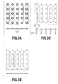
- the power distribution film is formed by pressing a metal plate in the shape shown in Fig. 3A .
- holes are formed in the power distribution film as the insulating film, and a terminal to be connected to a power source is formed in the power distribution film.
- penetration holes corresponding to the top side of the semiconductor light emitting elements may have a concave mirror-like shape as shown in Fig. 7 , thereby concentrating light and thus increasing luminance.
- material 701 such as resin or the like, known in the art is sealed into the penetration holes exposed to the outside in order protect the elements, as shown in Fig. 7 .
- the material 701 used for sealing may be silicon, epoxy or the like.
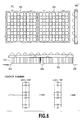
- a connection unit using a plurality of semiconductor light emitting modules may be configured by providing the modules with connections 601 interconnecting the modules, as shown in Fig. 6 .
- a connection unit using a plurality of semiconductor light emitting modules may be configured by providing the modules with connections 601 interconnecting the modules, as shown in Fig. 6 .
- modules manufactured according the following manufacturing method examples may be interconnected in the same way.
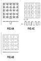
- Figs. 4A to 4C are views for explaining a method of manufacturing a semiconductor light emitting module using heat dissipation blocks prepared by metal plate bending or extrusion molding according to this embodiment.
- Fig. 4C shows heat dissipation fins 113 having a waveform-like shape by bending or extrusion molding.
- the heat dissipation fins 113 are arranged in parallel to each other, when the semiconductor light emitting module is disposed in such a manner that the heat dissipation fins 113 are vertically placed, air heated by the heat dissipation is raised along grooves of the fins, and thus convection of air having lower temperature, which is supplied from a lower side, occurs naturally, which results in promotion of heat dissipation.
- the effect obtained when the semiconductor light emitting elements are disposed to face downward is similar to that described above.
- the insulating film is formed by applying or coating an adhesive or the like having an insulation property on portions except for the semiconductor light emitting elements 111 on the top side of the heat dissipation blocks according to any method known in the art, as shown in Fig. 4B .
- the insulating film is prevented from being formed in portions corresponding to penetration holes and vents of the heat dissipation blocks.
- Figs. 5A to 5C are views for explaining a method of manufacturing a semiconductor light emitting module using heat dissipation blocks prepared by extrusion molding according to this embodiment.
- Fig. 5C shows heat dissipation blocks formed by extrusion molding in a normal direction of a loading surface of semiconductor light emitting elements. With such a shape, a process of forming vents after forming the blocks may be omitted.
- the effect obtained when the semiconductor light emitting elements are disposed to face downward is similar to that described above.
- Figs. 16A to 16D are views for explaining a method of manufacturing a semiconductor light emitting module using heat dissipation blocks prepared by cutting and erecting some of a metal plate according to this embodiment.
- Fig. 16C shows heat dissipation blocks formed by cutting and erecting some of a metal plate.
- the holes intended to generate the above-shown and described air current may not be required to be provided depending on the specification of a product, particularly a product including one semiconductor light emitting module or a plurality of semiconductor light emitting modules arranged in a line, or attachment sites or use environments of semiconductor light emitting modules, but the heat dissipation blocks may have a U-like or L-like section for achieving better effects.
- a terminal connected to a power source like the terminal formed in the above-described power distribution film.
- the power distribution film is formed using a metal plate having a shape shown in Fig. 16A .
- a portion exhibiting the function of the above-described reflection plate and being shown in Fig. 16D is formed by preparing individual reflecting parts.
- Material of these reflecting parts may be metal, resin or the like and may be manufactured by any appropriate method known in the art.
- the reflecting parts are prepared using metal and are pressed into the power distribution film formed by the metal plate for both of maintenance and conduction.
- the power distribution film is connected to the semiconductor light emitting elements by means of the conductive wires.
- any appropriate method known in the art such as using resin as material and plating a surface of the resin with conductive material.
- a conductive adhesive or the like may be used to fix the power distribution film and the reflecting parts.
- the semiconductor light emitting module 101 is not necessarily covered with an integrated case, but individual semiconductor light emitting elements 111 may be covered with respective cases, as described in this manufacturing method example.
- Penetration holes and vents of the power distribution film are formed in the same places and with the same shape as in the above manufacturing method example 1.
- the power distribution film is laminated like the above-described insulating film.
- the member 701 such as resin or the like is sealed in a way similar to that described above.
- the four kinds of manufacturing method examples have been described.
- the insulating film is formed in appropriate places of a conductive portion except for the connections of the semiconductor light emitting elements and a supply portion of the power source according to any method known in the art, and one of the manufacturing method examples is selected depending on use purpose and a packaging method of the product.
- Figs. 8A to 8D are conceptual views showing a structure of a semiconductor light emitting module manufactured according to another embodiment of the present invention.
- the semiconductor light emitting elements 111 are placed on a hollow cylindrical heat dissipation block and a semiconductor light emitting module is manufactured as in the above-described manufacturing method examples.
- the semiconductor light emitting elements are placed on a doughnut-like portion on the cylindrical heat dissipation block, the semiconductor light emitting elements may be placed without forming such a doughnut-like portion if the cylindrical heat dissipation block is sufficiently thick.
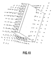
- Fig. 10 is a view showing feature of heat dissipation in case of use of a conventional semiconductor light emitting module
- Fig. 11 is a view showing feature of heat dissipation of a semiconductor light emitting module according to an embodiment of the present invention.
- the semiconductor light emitting module of the present invention used for measurement is that manufactured according to the manufacturing method example 1 of the first embodiment, and the measurement is made for the semiconductor light emitting module installed downward for ceiling illumination in Figs. 10 and 11 .
- Figs. 12 and 13 are views showing a thermal characteristic calculated in case of emission of light from a conventional semiconductor light emitting element and in case of emission of light from a semiconductor light emitting module manufactured according to the manufacturing method example 1 of the first embodiment, respectively.
- Fig. 12 shows the thermal characteristic when the semiconductor light emitting module is used for ceiling illumination
- Fig. 13 shows the thermal characteristic when the semiconductor light emitting module is used for wall illumination.
- the semiconductor light emitting module of the present invention for both of ceiling and wall can suppress increase of temperature even when an electrical input (input power) to the semiconductor light emitting module is increased.
- the semiconductor light emitting module of the present invention is directly formed on the heat dissipation blocks, it is possible to easily manufacture the module, reduce product costs and achieve high luminance emission by large current with highly-efficient heat dissipation.
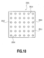
- FIG. 18 is a front view showing a structure of a semiconductor light emitting module according to this embodiment
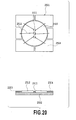
- Fig. 19 is a front view and a sectional view showing enlargement of a portion of the structure.
- a semiconductor light emitting module 2501 of this embodiment includes a high-reflection plate 2502 having functions of heat dissipation and light reflection, an insulating film 2503 covering the high-reflection plate 2502, and a power distribution film 2504 laminated via the insulating film 2503 and acting as an electrode.
- One or more semiconductor light emitting elements 2511 which are actually conducted to emit light are connected to the power distribution film 2504 via conductive wires 2512.
- the high-reflection plate 2502 has 95% or more, preferably 98% or more, of the overall reflectivity for sufficient emission of light.
- the high-reflection plate 2502 may be mounted by forming an adhesive layer on an aluminum base, forming a pure aluminum layer or a pure silver layer thereon, and forming a reflection-enhancing film thereon by depositing titanium oxide or silicon oxide. This reflection-enhancing film allows reduction of deterioration due to oxidation by inner pure aluminum or pure silver, thereby maintaining reflectivity longer than initial reflectivity, which may result in stabilization of product quality.
- the high-reflection plate 2502 may be manufactured by forming the reflection-enhancing film on metal finished into a desired shape by, for example, pressing or the like by depositing titanium oxide or silicon oxide on the above-described adhesive layer and pure aluminum layer or pure silver layer, or may be manufactured by forming the reflection-enhancing film on plate-like or coil-like metal and then finishing the film into a desired shape by pressing or the like.
- An example of this embodiment uses MIRO2-SILVER and MIRO2 available from ALANOD Company, which have 98% and 95% of the overall reflectivity, respectively.
- the high-reflection plate used in the present invention may be any appropriate reflection plate known in the art as long as it can achieve the object of the present invention, instead of the products available from ALANOD Company.
- the high-reflection plate 2502 may be employed as one electrode.
- the insulating film 2503 provides electrical isolation between at least the high-reflection plate 2502 and the power distribution film 2504, and may have any appropriate shape known in the art as long as it can include holes through which light emitted from the semiconductor light emitting elements 2511 is transmitted to the outside.
- the insulating film 2503 may be formed by inserting a substrate made of FR-4, polyimide or the like between the power distribution film 2504 and the high-reflection plate 2502 or by forming an insulating layer by adhering the power distribution film 2504 to the high-reflection plate 2502 by means of an insulating adhesive.
- Fig. 25B is a view for explaining an effect which does not exist in the prior art in case where the method of this example is employed.
- Fig. 25A showing a formation structure of a conventional general fluorescent substance or diffusion agent
- the structure of this example shown in Fig. 25B can make the fluorescent substance or diffusion agent uniform, it is possible to further reduce loss of light as compared to the conventional structure.
- Fig. 25A it is difficult to obtain uniform white or diffused light since the content of fluorescent substance or diffusion agent is different depending direction of light emitted from the semiconductor light emitting elements 2511.
- a circular concave groove 2801 on the high-reflection plate 2502 around the semiconductor light emitting element 2511 and forming the dome 2802 thereon using a surface tension of the resin a uniform resin layer is formed around the semiconductor light emitting element 2511 such that light passes through the resin by the same distance.
- the concave groove 2801 may have any size, position and shape as long as it can use a surface tension of the resin and may be formed by, for example, pressing or any appropriate method known in the art.
- the semiconductor light emitting module includes the heat dissipation blocks which become one electrode to supply power to semiconductor light emitting elements arranged in contact with surfaces of the heat dissipation blocks, the insulating film which covers any portions of the surfaces of the heat dissipation blocks except for the semiconductor light emitting elements and the neighborhood thereof, and the power distribution film which is disposed in contact with any surface of the insulating film, is electrically connected to the semiconductor light emitting elements, and becomes the other electrode to supply power, it is possible to provide a semiconductor light emitting module and device and a method of manufacturing the same, which are capable of preventing luminance characteristics from being deteriorated even when large current is flown, thereby achieving high luminance, by suppressing temperature from being increased by dissipating heat, which is generated in the semiconductor light emitting elements, with high efficiency. In addition, it is possible to maintain higher reflectivity to obtain uniform white light and increase emission efficiency of light to achieve light emission with high luminance.
Landscapes
- Engineering & Computer Science (AREA)
- General Engineering & Computer Science (AREA)
- Physics & Mathematics (AREA)
- Microelectronics & Electronic Packaging (AREA)
- Optics & Photonics (AREA)
- Led Device Packages (AREA)
- Led Devices (AREA)
Abstract
Description
- The present invention relates to a semiconductor light emitting module and device and a method of manufacturing the same, and more particularly, to a semiconductor light emitting module and device and a method of manufacturing the same, which enable high luminance light emission by high power.
- In recent years, there have been developed a variety of devices using semiconductor light emitting elements, such as light emitting diodes (LEDs) and the like, having high energy efficiency for emission in a variety of fields. In particular, LEDs for illumination with use of large current, as substitutes for conventional fluorescent lamps and incandescent electric lamps, have attracted great attention, and techniques for overcoming problems of heat generation, which are caused by large current, have been proposed.
- For example, a technique for radiating heat with high efficiency, with electrodes directly connected to semiconductor light emitting elements, which generate heat, as heat radiation blocks, has been proposed (for example, see Patent Document 1).
- In the meantime, a technique of a semiconductor light emitting unit for illumination, which uses a plurality of semiconductor light emitting elements as a light source and has a constant area close to a surface light source other than a point light source, with high intensity of light radiation, has been proposed (for example, see Patent Document 2).
- In addition, a technique of employing silver plating with high reflection efficiency for a LED mount pattern has been proposed, and, particularly for white light, a technique for increasing light emission efficiency with combination of blue or near-ultraviolet LEDs with a fluorescent substance has been proposed (for example, see Patent Document 3).
- However, the convention technique of employing an array of plural semiconductor light emitting elements for a light source has a problem of poor efficiency of heat radiation since a substrate or the like is interposed between a heat radiation block and the elements. In addition, a conventional manufacturing method has a problem of high production costs since elements are arranged on a substrate and then a member such as a heat radiation block or the like is combined to the elements.
- In addition, since the silver plating is typically carried out after a pattern is formed, enhancement of reflectivity is limited, not a few non-reflecting surfaces occur due to the formation of the pattern, a sliver-plated surface is easily oxidized, and further it is difficult to maintain initial reflectivity due to change of reflectivity with time. In addition, since the content of fluorescent substance or diffusion agent is not uniform, light emitted in a direction with higher content of fluorescent substance or diffusion agent undergoes large light loss depending on direction of light emitted from LEDs, which makes it impossible to increase emission efficiency of light.
- In consideration of the above-mentioned problems, it is an object of the invention to provide a semiconductor light emitting module and device and a method of manufacturing the same, which are capable of preventing luminance characteristics from being deteriorated even when large current is flown, thereby achieving high luminance, by suppressing temperature from being increased by dissipating heat, which is generated in semiconductor light emitting elements, with high efficiency.
- It is another object of the invention to maintain higher reflectivity to obtain uniform white light and increase emission efficiency of light to achieve light emission with high luminance.
-
- [Patent Document 1] Japanese Patent Laid-Open No.
2002-223007 - [Patent Document 2] Japanese Patent Laid-Open No.
2002-93206 - [Patent Document 3] Japanese Patent Laid-Open No.
H10-242513 - In order to achieve the above-mentioned objects, according to an aspect of the invention, there is provided a semiconductor light emitting module including: semiconductor light emitting elements; a heat dissipation block which becomes one electrode to supply power to the semiconductor light emitting elements disposed in contact with a surface of the heat dissipation block; an insulating film which covers any portion of the surface of the heat dissipation block except for the semiconductor light emitting elements and neighborhoods thereof; and a power distribution film which is disposed in contact with any surface of the insulating film, is electrically connected to the semiconductor light emitting elements, and becomes the other electrode to supply power.
- Preferably, each of the neighborhoods of the semiconductor light emitting elements has a reflection plate-like shape to reflect and concentrate light emitted from each of the semiconductor light emitting elements.
- Preferably, the heat dissipation block has a slit structure such that air convection to promote heat dissipation is not interrupted.
- Preferably, the heat dissipation block has holes to produce an air current to promote dissipation of heat from the heat dissipation block.
- Preferably, the insulating film and the power distribution film have holes to produce an air current to promote dissipation of heat from the heat dissipation block.
- Preferably, one or more sets of power supply terminals are included in one or both of any positions of the heat dissipation block which becomes one electrode to supply power to the semiconductor light emitting elements and the power distribution film which becomes the other electrode to supply the power.
- According to another aspect of the invention, there is provided a semiconductor light emitting device including: a semiconductor light emitting module including semiconductor light emitting elements, a heat dissipation block which becomes one electrode to supply power to the semiconductor light emitting elements disposed in contact with a surface of the heat dissipation block, an insulating film which covers any portion of the surface of the heat dissipation block except for the semiconductor light emitting elements and neighborhoods thereof, and a power distribution film which is disposed in contact with any surface of the insulating film, is electrically connected to the semiconductor light emitting elements, and becomes the other electrode to supply power; and a housing including a power source to supply power to the semiconductor light emitting elements, and a supporting means to support the semiconductor light emitting module.
- Preferably, the semiconductor light emitting device further includes an illumination hood having a heat dissipation part and being connected to the heat dissipation block.
- According to still another aspect of the invention, there is provided a method of manufacturing a semiconductor light emitting module, including the steps of: disposing semiconductor light emitting elements in contact with a surface of a heat dissipation block which becomes one electrode to supply power to the semiconductor light emitting elements; covering any portion of the surface of the heat dissipation block with an insulating film except for the semiconductor light emitting elements and neighborhoods thereof; and disposing a power distribution film in contact with any surface of the insulating film, the power distribution film being electrically connected to the semiconductor light emitting elements and being the other electrode to supply the power.
- Preferably, the method further includes the step of manufacturing the heat dissipation block by pressing a metal plate into a waveform shape.
- Preferably, the method further includes the step of forming the heat dissipation block by means of an extruded frame member by extruding the heat dissipation block in a direction normal to a surface on which the semiconductor light emitting elements are disposed.
- Preferably, the method further includes the step of manufacturing the heat dissipation block by cutting erecting a portion of a metal plate.
- According to still another aspect of the invention, there is provided a semiconductor light emitting module including: semiconductor light emitting elements; a high-reflection plate which is formed to reflect light from the semiconductor light emitting elements by depositing a reflection-enhancing film thereon, the semiconductor light emitting elements being disposed in contact with a surface of the high-reflection plate; an insulating film which covers any portion of the surface of the high-reflection plate except for the semiconductor light emitting elements and neighborhoods thereof; and a power distribution film which is disposed in contact with any surface of the insulating film, is electrically connected to the semiconductor light emitting elements, and becomes the other electrode to supply power.
-
- [
Fig. 1] Fig. 1 is a front view showing a structure of a semiconductor light emitting module according to an embodiment of the present invention. - [
Fig. 2] Fig. 2 is a front view showing a structure of a semiconductor light emitting module according to an embodiment of the present invention. - [
Fig. 3A] Fig. 3A is a view for explaining a method of manufacturing a semiconductor light emitting module using a heat dissipation block prepared by extrusion molding according to an embodiment of the present invention. - [
Fig. 3B] Fig. 3B is a view for explaining a method of manufacturing a semiconductor light emitting module using a heat dissipation block prepared by extrusion molding according to an embodiment of the present invention. - [
Fig. 3C] Fig. 3C is a view for explaining a method of manufacturing a semiconductor light emitting module using a heat dissipation block prepared by extrusion molding according to an embodiment of the present invention. - [
Fig. 4A] Fig. 4A is a view for explaining a method of manufacturing a semiconductor light emitting module using a heat dissipation block prepared by metal plate bending or extrusion molding according to an embodiment of the present invention. - [
Fig. 4B] Fig. 4B is a view for explaining a method of manufacturing a semiconductor light emitting module using a heat dissipation block prepared by metal plate bending or extrusion molding according to an embodiment of the present invention. - [
Fig. 4C] Fig. 4C is a view for explaining a method of manufacturing a semiconductor light emitting module using a heat dissipation block prepared by metal plate bending or extrusion molding according to an embodiment of the present invention. - [
Fig. 5A] Fig. 5A is a view for explaining a method of manufacturing a semiconductor light emitting module using a heat dissipation block prepared by extrusion molding according to an embodiment of the present invention. - [
Fig. 5B] Fig. 5B is a view for explaining a method of manufacturing a semiconductor light emitting module using a heat dissipation block prepared by extrusion molding according to an embodiment of the present invention. - [
Fig. 5C] Fig. 5C is a view for explaining a method of manufacturing a semiconductor light emitting module using a heat dissipation block prepared by extrusion molding according to an embodiment of the present invention. - [
Fig. 6] Fig. 6 is a front view showing a structure of a semiconductor light emitting module according to an embodiment of the present invention. - [
Fig. 7] Fig. 7 is a front view showing a structure of a semiconductor light emitting module according to an embodiment of the present invention. - [
Fig. 8A] Fig. 8A is a conceptual view showing a semiconductor light emitting module manufactured according to another embodiment of the present invention. - [
Fig. 8B] Fig. 8B is a conceptual view showing a semiconductor light emitting module manufactured according to still another embodiment of the present invention. - [
Fig. 8C] Fig. 8C is a conceptual view showing a semiconductor light emitting module manufactured according to still another embodiment of the present invention. - [
Fig. 8D] Fig. 8D is a conceptual view showing a semiconductor light emitting module manufactured according to another embodiment of the present invention. - [
Fig. 9] Fig. 9 is a schematic view showing an illuminator having semiconductor light emitting modules according to another embodiment of the present invention. - [
Fig. 10] Fig. 10 is a view showing feature of heat dissipation in case of use of a conventional semiconductor light emitting module. - [
Fig. 11] Fig. 11 is a view showing feature of heat dissipation of a semiconductor light emitting module according to an embodiment of the present invention. - [
Fig. 12] Fig. 12 is a view showing a thermal characteristic in case of emission of light from a conventional semiconductor light emitting element for ceiling illumination and in case of emission of light from a semiconductor light emitting module for ceiling illumination according to an embodiment of the present invention. - [
Fig. 13] Fig. 13 is a view showing a thermal characteristic in case of emission of light from a conventional semiconductor light emitting element for wall illumination and in case of emission of light from a semiconductor light emitting module for wall illumination according to an embodiment of the present invention. - [
Fig. 14] Fig. 14 is a view showing a thermal characteristic in case of emission of light from a semiconductor light emitting element for ceiling illumination according to a first embodiment of the present invention. - [
Fig. 15] Fig. 15 is a view showing a thermal characteristic in case of emission of light from a semiconductor light emitting element for wall illumination according to a first embodiment of the present invention. - [
Fig. 16A] Fig. 16A is a view for explaining a method of manufacturing a semiconductor light emitting module using a heat dissipation block prepared by cutting and erecting some of a metal plate according to an embodiment of the present invention. - [
Fig. 16B] Fig. 16B is a view for explaining a method of manufacturing a semiconductor light emitting module using a heat dissipation block prepared by cutting and erecting some of a metal plate according to an embodiment of the present invention. - [
Fig. 16C] Fig. 16C is a view for explaining a method of manufacturing a semiconductor light emitting module using a heat dissipation block prepared by cutting and erecting some of a metal plate according to an embodiment of the present invention. - [
Fig. 16D] Fig. 16D is a view for explaining a method of manufacturing a semiconductor light emitting module using a heat dissipation block prepared by cutting and erecting some of a metal plate according to an embodiment of the present invention. - [
Fig. 17A] Fig. 17A is a view showing an example of multidirectional heat dissipation fins of a heat dissipation block prepared by cutting and erecting some of a metal plate according to an embodiment of the present invention. - [
Fig. 17B] Fig. 17B is a view showing an example of multidirectional heat dissipation fins of a heat dissipation block prepared by cutting and erecting some of a metal plate according to an embodiment of the present invention. - [
Fig. 17C] Fig. 17C is a view showing an example of multidirectional heat dissipation fins of a heat dissipation block prepared by cutting and erecting some of a metal plate according to an embodiment of the present invention. - [
Fig. 17D] Fig. 17D is a view showing an example of multidirectional heat dissipation fins of a heat dissipation block prepared.by cutting and erecting some of a metal plate according to an embodiment of the present invention. - [
Fig. 18] Fig. 18 is a front view showing a structure of a semiconductor light emitting module according to an embodiment of the present invention. - [
Fig. 19] Fig. 19 is a partially enlarged front view and a partially enlarged sectional view showing another structure of a semiconductor light emitting module according to an embodiment of the present invention. - [
Fig. 20] Fig. 20 is a front view and a cross side view showing another structure of a semiconductor light emitting module according to an embodiment of the present invention. - [
Fig. 21] Fig. 21 is a front view and a cross side view showing still another structure of a semiconductor light emitting module according to an embodiment of the present invention. - [
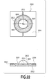
Fig. 22] Fig. 22 is a front view and a cross side view showing still another structure of a semiconductor light emitting module according to an embodiment of the present invention. - [
Fig. 23] Fig. 23 is a front view and a cross side view showing still another structure of a semiconductor light emitting module according to an embodiment of the present invention. - [
Fig. 24] Fig. 24 is a view showing an example of a case of a semiconductor light emitting module according to an embodiment of the present invention. - [
Fig. 25A] Fig. 25A is a view showing a conventional configuration for explanation of an effect which does not exist in the prior art in case where an exemplary method of an embodiment of the present invention is employed. - [
Fig. 25B] Fig. 25B is a view showing a configuration of an embodiment of the present invention for explanation of an effect which does not exist in the prior art in case where an exemplary method of the embodiment of the present invention is employed. - [
Fig. 26] Fig. 26 is a view showing a result of measurement of luminance using materials of three kinds of reflection plates in order to check an effect of the present invention. - [
Fig. 27] Fig. 27 is a view for explaining suppression of attenuation of the amount of reflected light after repetition of reflection with increase of reflectivity of a reflection plate according to an embodiment of the present invention. - [
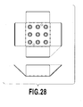
Fig. 28] Fig. 28 is a view showing a deployed reflection structure according to an embodiment of the present invention. - [
Fig. 29A] Fig. 29A is a view showing a result of test for change of emission efficiency with time according to an embodiment of the present invention. - [
Fig. 29B] Fig. 29B is a view showing a result of test for change of emission efficiency with time according to an embodiment of the present invention. - [
Fig. 29C] Fig. 29C is a view showing a result of test for change of emission efficiency with time according to an embodiment of the present invention. - Hereinafter, embodiments of the present embodiment will be described in detail with reference to the drawings.
-
Fig. 1 is a front view showing a structure of a semiconductor light emitting module according to an embodiment of the present invention. A semiconductorlight emitting module 101 according to this embodiment includes heat dissipation blocks 102 for heat dissipation and also acting as one electrode, an insulatingfilm 103 covering the heat dissipation blocks 102 for insulation, and apower distribution film 104 which is additionally laminated via the insulatingfilm 103 and also acts as another electrode. One terminal of each of semiconductorlight emitting elements 111 through which current flows for emission of light is electrically and directly connected to the heat dissipation blocks 102 and the other terminal of each of them is connected to thepower distribution film 104 via a correspondingconductive wire 112. - The heat dissipation blocks 102 may be made of any materials and may have any shape as long as they have a heat dissipation property for heat dissipation media and an electrical property for an electrode. For example, in this embodiment, the heat dissipation blocks 102 may be made of metal such as iron, silver, copper, aluminum or the like, alloy thereof, a carbon-based material having thermal conductivity higher than that of metal, or a compound material thereof in various manners. Also, for example, the heat dissipation blocks 102 may have a shape like projecting heat dissipation fins as shown in
Figs. 3A to 3C , a slit shape which does not obstruct air convection promoting heat dissipation, or a shape like a waveform when viewed in a horizontal direction as shown inFigs. 4A to 4C . In addition, as will be described later, the heat dissipation blocks may be worked and shaped by an extruded frame member, or may be prepared by metal plate bending, or may be formed using any appropriate methods known in the art without any limitation as long as they can achieve the object of the present invention. - In addition, in order to more effectively achieve the heat dissipation, the heat dissipation blocks 102 may have vents as shown in
Figs. 3A to 3C or the waveform as shown inFigs. 4A to 4C to allow an air current to flow. In this case, the insulatingfilm 103 and thepower distribution film 104 has corresponding vents in compliance with such a structure. - In addition, the heat dissipation blocks 102 themselves are prepared to have the function of the
heat dissipation fins 113, but without being limited thereto, they may be prepared to be integrated with separately-preparedheat dissipation fins 113 for the reason of manufacture. In addition, it is preferable that places of the heat dissipation blocks 102 where the semiconductorlight emitting elements 111 are connected to the heat dissipation blocks 102 are subjected to surface plating known in the art. In addition, the material of the separately-preparedheat dissipation fins 113 does not necessarily have the electrical property for the above-described electrode, but may be, for example, ceramics or plastics. - The insulating
film 103 may be any insulating film known in the art as long as it can provide electrical isolation between at least the heat dissipation blocks 102 and thepower distribution film 104 and has holes through which light emitted from at least the semiconductorlight emitting elements 111 are emitted to the outside. For example, a substrate made of FR4 or polyimide having a shape as shown inFig. 3B may be interposed between thepower distribution film 104 and the heat dissipation blocks 102 to form the insulatingfilm 103, or thepower distribution film 104 and the heat dissipation blocks 102 are adhered to each other by means of an adhesive having an insulation property to form an insulating layer, that is, the insulatingfilm 103. - The
power distribution film 104 may be, for example, a worked metal plate as shown inFig. 3A , or a metal film formed by plating the insulatingfilm 103 formed on or attached to the heat dissipation blocks 102 as long as it is formed to provide an electrode having polarity different from that of the heat dissipation blocks 102 of the semiconductorlight emitting elements 111. When thepower distribution film 104 is prepared by the metal plate, penetration holes have to be provided in portions corresponding to the top side of the semiconductorlight emitting elements 111 such that the light emitted from at least the semiconductorlight emitting elements 111 are not interrupted. In this case, the shape and size of the penetration holes are determined by any method known in the art. In addition, when thepower distribution film 104 is provided by the plating, a metal film is formed by any appropriate method known in the art in such a manner that it has penetration holes while covering the insulatingfilm 103. - Of course, it is also possible to form the insulating
film 103 and thepower distribution film 104 using a typical print board. - After forming the
power distribution film 104, the semiconductorlight emitting elements 111 and thepower distribution film 104 are electrically connected by theconductive wires 112, and power supplied from a power source through a terminal 114 provided at a portion of thepower distribution film 104 is supplied to one pole of each of the semiconductorlight emitting elements 111 through theconductive wires 112. It is shown in this embodiment that the semiconductorlight emitting elements 111 and thepower distribution film 104 are interconnected by theconductive wires 112, however, without being limited thereto, various other method may be used to electrically connect thepower distribution film 104 with the semiconductorlight emitting elements 111 while forming thepower distribution film 104 without using theconductive wires 112. For example, with plating using an insulating film having an appropriate shape, it is possible to form a metal film in compliance with the shape and connect the metal film with the semiconductorlight emitting elements 111. In addition, the shape and structure of the terminal 114 may be any shape and structure known in the art, and may be attached, as a separate part, to thepower distribution film 104. - In addition, it is preferable that the place of the
power distribution film 104 where theconductive wires 112 are connected to thepower distribution film 104 is subjected to surface plating known in the art. - The penetration holes provided in the
power distribution film 104 may have any shape as long as they do not obstruct the light emitted from the semiconductorlight emitting elements 111. For example, the penetration holes may be formed to concentrate light by employing a reflecting plate-like shape as can be understood from a sectional view shown inFig. 7 . In this case, it is possible to easily seal resin or the like into the penetration holes in order to protect the semiconductorlight emitting elements 111. - In addition, in order to concentrate light by putting the shape of the penetration holes provided in the above-described
power distribution film 104 into the reflection plate-like shape, it is possible to combine separately-prepared parts having the function of reflection plate with thepower distribution film 104. In this case, by making the parts having the function of reflection plate conductive, it is possible to connect the parts with the above-describedconductive wires 112. - Although the basic structure of the semiconductor
light emitting module 101 according to this embodiment has been illustrated in the above with reference toFig. 1 , the light emitted from the semiconductorlight emitting elements 111 may be concentrated by covering the semiconductorlight emitting module 101 with acase 202 in actuality, as shown inFig. 2 . Thecase 202 may be made of material such as polycarbonate, acryl, or glass, but without being limited thereto, may be made of any material known in the art and may have any shape. In addition, if the use of thecase 202 provides sufficient protection for the semiconductor light emitting module, the above-mentioned resin or the like may not be sealed. - A method of manufacturing the semiconductor light emitting module as constructed above will be described with reference to
Figs. 3 to 5 . Modules shown inFigs. 3 to 5 each represent a power distribution film, an insulating film and heat dissipation blocks. For example, the power distribution film, the insulating film and the heat dissipation blocks are shown in the form of a top view and a front view inFigs. 3A, 3B and 3C , respectively. - A manufacturing method Example 1 according to this embodiment will be first described with reference to
Figs. 3A to 3C. Figs. 3A to 3C are views for explaining a method of manufacturing a semiconductor light emitting module using heat dissipation blocks prepared by extrusion molding according to this embodiment.Fig. 3C shows heat dissipation blocks provided by subjecting them to extrusion molding and then by forming vents by perforating process, whereheat dissipation fins 113 are arranged in parallel to each other. Since theheat dissipation fins 113 are arranged in parallel to each other, when the semiconductor light emitting module is disposed in such a manner that theheat dissipation fins 113 are vertically placed, air heated by the heat dissipation is raised along grooves of the fins, and thus convection of air having lower temperature, which is supplied from a lower side, occurs naturally, which results in promotion of heat dissipation. - In addition, when the semiconductor light emitting elements are disposed to face downward like an illuminator installed on a ceiling or the like, air heated by the
heat dissipation fins 113 increases, but convection of new air having lower temperature occurs due to the above-mentioned vents, which also results in promotion of heat dissipation. - Next, a substrate made of material such as FR4, polyimide having a shape as shown in
Fig. 3B is prepared as the insulating film. When the substrate is prepared, holes are formed in portions of the semiconductorlight emitting elements 111 and portions of vents of the heat dissipation blocks. The prepared substrate is laminated on the above-described heat dissipation blocks. The substrate may be laminated by any adhesion or lamination method known in the art. - In addition, the power distribution film is formed by pressing a metal plate in the shape shown in
Fig. 3A . At this time, holes are formed in the power distribution film as the insulating film, and a terminal to be connected to a power source is formed in the power distribution film. In this case, penetration holes corresponding to the top side of the semiconductor light emitting elements may have a concave mirror-like shape as shown inFig. 7 , thereby concentrating light and thus increasing luminance. - The semiconductor
light emitting elements 111 are directly placed on the heat dissipation blocks through the penetration holes of the prepared power distribution film. One side of each of theconductive wires 112 is combined to each of the semiconductorlight emitting elements 111 and the other side of eachconductive wire 112 is combined to an appropriate site near the penetration holes of the power distribution film. Although the semiconductor light emitting elements are disposed after laminating the power distribution film in this embodiment, the semiconductor light emitting elements may be first disposed on the heat dissipation blocks. - Although the semiconductor light emitting module as prepared above has its own essential function in that state,
material 701, such as resin or the like, known in the art is sealed into the penetration holes exposed to the outside in order protect the elements, as shown inFig. 7 . Herein, thematerial 701 used for sealing may be silicon, epoxy or the like. - While the semiconductor light emitting module is manufactured according to the manufacturing method Example 1 in this manner, a connection unit using a plurality of semiconductor light emitting modules may be configured by providing the modules with
connections 601 interconnecting the modules, as shown inFig. 6 . In this embodiment, by providing the connection unit by interconnecting the modules by means of anelectrode terminal 604 other than theconnections 601, light may be emitted when the connection unit is connected to a power source. In addition, modules manufactured according the following manufacturing method examples may be interconnected in the same way. - Next, a manufacturing method Example 2 according to this embodiment will be described with reference to
Figs. 4A to 4C. Figs. 4A to 4C are views for explaining a method of manufacturing a semiconductor light emitting module using heat dissipation blocks prepared by metal plate bending or extrusion molding according to this embodiment.Fig. 4C showsheat dissipation fins 113 having a waveform-like shape by bending or extrusion molding. Since theheat dissipation fins 113 are arranged in parallel to each other, when the semiconductor light emitting module is disposed in such a manner that theheat dissipation fins 113 are vertically placed, air heated by the heat dissipation is raised along grooves of the fins, and thus convection of air having lower temperature, which is supplied from a lower side, occurs naturally, which results in promotion of heat dissipation. In addition, the effect obtained when the semiconductor light emitting elements are disposed to face downward is similar to that described above. - Next, the insulating film is formed by applying or coating an adhesive or the like having an insulation property on portions except for the semiconductor
light emitting elements 111 on the top side of the heat dissipation blocks according to any method known in the art, as shown inFig. 4B . By doing so, the insulating film is prevented from being formed in portions corresponding to penetration holes and vents of the heat dissipation blocks. - In addition, an insulating layer may be formed as the insulating film by performing printing having an insulating property and a function of an adhesive.
- In addition, the power distribution film may be formed by forging, pressing, cutting or the like a metal plate having a shape as shown in
Fig. 4A . Penetration holes and vents of the power distribution film are formed in the same places and with the same shape as in the above manufacturing method example 1. The power distribution film is laminated like the above-described insulating film, and the semiconductorlight emitting elements 111 are placed on the power distribution film, and theconductive wires 112 are combined to appropriate places near the penetration holes. Themember 701 such as resin or the like is sealed in a way similar to that described above. - Next, a manufacturing method Example 3 according to this embodiment will be described with reference to
Figs. 5A to 5C. Figs. 5A to 5C are views for explaining a method of manufacturing a semiconductor light emitting module using heat dissipation blocks prepared by extrusion molding according to this embodiment.Fig. 5C shows heat dissipation blocks formed by extrusion molding in a normal direction of a loading surface of semiconductor light emitting elements. With such a shape, a process of forming vents after forming the blocks may be omitted. In addition, the effect obtained when the semiconductor light emitting elements are disposed to face downward is similar to that described above. - Next, a substrate is prepared as the insulating film by injection molding or sheet casting according to any method known in the art, as shown in
Fig. 5B , and then is laminated on the heat dissipation blocks as in the manufacturing method example 1. In addition, when the insulating film is prepared by the injection molding, by forming bosses in appropriate places on the insulating film and providing through holes in appropriate places of the power distribution film and the heat dissipation blocks, the insulating film can be laminated by thermal caulking alone, in combination of adhesion, or any adhesion or lamination method known in the art, such as insert molding of the insulating film into the power distribution film and the heat dissipation blocks. - In addition, as shown in
Fig. 7 , the power distribution film is formed by mutually attaching a plurality of metal plates. Penetration holes and vents of the power distribution film are formed in the same places and with the same shape as in the above manufacturing method example 1. The power distribution film is laminated like the above-described insulating film, and the semiconductorlight emitting elements 111 are placed on the power distribution film, and theconductive wires 112 are combined to appropriate places near the penetration holes. Themember 701 such as resin or the like is sealed in a way similar to that described above. - Next, a manufacturing method Example 4 according to this embodiment will be described with reference to
Figs. 16A to 16D. Figs. 16A to 16D are views for explaining a method of manufacturing a semiconductor light emitting module using heat dissipation blocks prepared by cutting and erecting some of a metal plate according to this embodiment.Fig. 16C shows heat dissipation blocks formed by cutting and erecting some of a metal plate. When the semiconductor light emitting module is disposed in such a manner that the formedheat dissipation fins 113 are vertically placed, air heated by the heat dissipation is raised along the fins, and thus convection of air having lower temperature, which is supplied from a lower side, occurs naturally, which results in promotion of heat dissipation. In addition, the effect obtained when the semiconductor light emitting module is disposed to face downward is similar to that described above. - The metal plate may be cut and erected by means of a pressing method. Alternatively, the metal plate may be formed by cutting and erecting pin portions by laser cut or etching or any appropriate method known in the art.
- An angle of cutting and erecting is not limited to 90°C, but, for example, the metal plate may be erected in an emission direction of the semiconductor light emitting elements. In addition, the cutting and erecting is not necessarily carried out in an initial step of the process, but may be carried out in the course of disposing the semiconductor light emitting elements or in a final step of the process. In addition, the heat dissipation fins formed by the cutting and erecting do not direct necessarily to the same direction, but, for example, may be formed into a concentric shape in case of a circular product like a circular model shown in
Figs. 17C to 17D . - In addition, the holes intended to generate the above-shown and described air current may not be required to be provided depending on the specification of a product, particularly a product including one semiconductor light emitting module or a plurality of semiconductor light emitting modules arranged in a line, or attachment sites or use environments of semiconductor light emitting modules, but the heat dissipation blocks may have a U-like or L-like section for achieving better effects. In addition, although not shown, it is possible to form a terminal connected to a power source like the terminal formed in the above-described power distribution film.
- Next, a substrate is prepared as the insulating film by using material, such as polyimide or the like, having a shape shown in
Fig. 16B and is then laminated on the heat dissipation blocks as in the manufacturing method example 1. - After such lamination, the power distribution film is formed using a metal plate having a shape shown in
Fig. 16A . Here, a portion exhibiting the function of the above-described reflection plate and being shown inFig. 16D is formed by preparing individual reflecting parts. Material of these reflecting parts may be metal, resin or the like and may be manufactured by any appropriate method known in the art. In this manufacturing method example, the reflecting parts are prepared using metal and are pressed into the power distribution film formed by the metal plate for both of maintenance and conduction. Thereafter, the power distribution film is connected to the semiconductor light emitting elements by means of the conductive wires. Of course, there may be used any appropriate method known in the art such as using resin as material and plating a surface of the resin with conductive material. In addition, a conductive adhesive or the like may be used to fix the power distribution film and the reflecting parts. - Although it has been illustrate in the above that light emitted from the semiconductor
light emitting elements 111 is concentrated by covering the semiconductorlight emitting module 101 with thecase 202,' the semiconductorlight emitting module 101 is not necessarily covered with an integrated case, but individual semiconductorlight emitting elements 111 may be covered with respective cases, as described in this manufacturing method example. Penetration holes and vents of the power distribution film are formed in the same places and with the same shape as in the above manufacturing method example 1. The power distribution film is laminated like the above-described insulating film. Themember 701 such as resin or the like is sealed in a way similar to that described above. In addition, it is also possible to further increase a heat dissipation effect by cutting and erecting the power distribution film. - Here, if the manufacturing method example 4 uses a etching process, it is possible to prepare a semiconductor light emitting module with high dimension precision by using and working a laminate of the above-described metal plate, the insulating film and another metal plate.
- Hitherto, the four kinds of manufacturing method examples have been described. In any manufacturing method example, it may be preferable that the insulating film is formed in appropriate places of a conductive portion except for the connections of the semiconductor light emitting elements and a supply portion of the power source according to any method known in the art, and one of the manufacturing method examples is selected depending on use purpose and a packaging method of the product. In addition, it is preferable to use material with high thermal conductivity and emissivity for the insulating film.
-
Figs. 8A to 8D are conceptual views showing a structure of a semiconductor light emitting module manufactured according to another embodiment of the present invention. As shown inFig. 8A , the semiconductorlight emitting elements 111 are placed on a hollow cylindrical heat dissipation block and a semiconductor light emitting module is manufactured as in the above-described manufacturing method examples. Although it is shown inFigs. 8A to 8D that the semiconductor light emitting elements are placed on a doughnut-like portion on the cylindrical heat dissipation block, the semiconductor light emitting elements may be placed without forming such a doughnut-like portion if the cylindrical heat dissipation block is sufficiently thick. - When the semiconductor light emitting module manufactured so is used in a direction shown in
Fig. 8B , air heated by heat dissipation goes out of a hollow portion of the cylindrical heat dissipation block, thereby producing natural air convection, which results in promotion of heat dissipation. In addition, as shown inFig. 8C , by providing a plurality of air vents in the heat dissipation block or making the heat dissipation block in the shape of mesh, natural air convection is produced to promote heat dissipation even when the semiconductor light emitting module is placed in a horizontal direction. In addition, by connecting the heat dissipation block to an umbrella-like portion 801 shown inFig. 8D , natural convection is produced near the umbrella-like portion 801, which may result in more effective heat dissipation without passing air through the cylindrical heat dissipation block. In this case, since holes are not formed in the top side of the cylindrical heat dissipation block, dusts are prevented from being introduced in the cylindrical heat dissipation block used for an illuminator. - Hitherto, the structure of the semiconductor light emitting modules having different shapes and materials and the method of manufacturing the same have been illustrated. Components such as the heat dissipation block having the shape and material used for these modules may be combined to form different kinds of modules. Accordingly, the present invention can provide a variety of semiconductor light emitting modules having characteristics of various components. These semiconductor light emitting modules may be used as not only illuminators but also various light emitting materials for signaling and the like.
-
Fig. 10 is a view showing feature of heat dissipation in case of use of a conventional semiconductor light emitting module, andFig. 11 is a view showing feature of heat dissipation of a semiconductor light emitting module according to an embodiment of the present invention. Here, the semiconductor light emitting module of the present invention used for measurement is that manufactured according to the manufacturing method example 1 of the first embodiment, and the measurement is made for the semiconductor light emitting module installed downward for ceiling illumination inFigs. 10 and11 . - In comparison of
Fig. 10 withFig. 11 , it can be seen that air convection is produced near the heat dissipation blocks in the semiconductor light emitting module, thereby achieving heat dissipation with high efficiency without collection of heat generated from semiconductor light emitting elements in the module, unlike the conventional semiconductor light emitting module. - In addition,
Figs. 12 and13 are views showing a thermal characteristic calculated in case of emission of light from a conventional semiconductor light emitting element and in case of emission of light from a semiconductor light emitting module manufactured according to the manufacturing method example 1 of the first embodiment, respectively.Fig. 12 shows the thermal characteristic when the semiconductor light emitting module is used for ceiling illumination andFig. 13 shows the thermal characteristic when the semiconductor light emitting module is used for wall illumination. As can be seen fromFigs. 12 and13 , as compared to a case where the conventional semiconductor light emitting module is used for both of ceiling and wall, the semiconductor light emitting module of the present invention for both of ceiling and wall can suppress increase of temperature even when an electrical input (input power) to the semiconductor light emitting module is increased. -
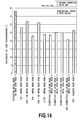
Figs. 14 and15 are views showing temperature in case of light emission with constant power according to the first embodiment.Fig. 14 shows a simulation for temperature of semiconductor light emitting elements when current is flown to emit light in case where a conventional semiconductor light emitting module is used for ceiling illumination and in case where the semiconductor light emitting modules according to the various embodiments of the present invention are used for ceiling illumination.Fig. 15 shows a simulation for temperature of semiconductor light emitting elements when current is flown to emit light in case where a conventional semiconductor light emitting module is used for wall illumination and in case where the semiconductor light emitting modules according to the various embodiments of the present invention are used for wall illumination. As can be seen fromFigs. 14 and15 , as compared to the case where the conventional semiconductor light emitting module is used, the semiconductor light emitting modules according to the various embodiments of the present invention can decrease temperature. - In this manner, since the semiconductor light emitting module of the present invention is directly formed on the heat dissipation blocks, it is possible to easily manufacture the module, reduce product costs and achieve high luminance emission by large current with highly-efficient heat dissipation.
- While the above first embodiment can provide highly-efficient heat dissipation of the light emitting module and high luminance by using large current, a second embodiment of the present invention is to provide illumination with high luminance and increase emission efficiency of light by combining a reflecting plate and a fluorescent substance. This second embodiment can be used for not only illuminators but also signals and the like, as illustrated with the light emitting module of the first embodiment, and can show more remarkable effects by itself or in combination of the first embodiment. For example, while simple provision of a reflecting plate or the like in the light emitting module of the first embodiment may deteriorate a heat dissipation characteristic and make it difficult to obtain high luminance, this second embodiment to increase reflectivity allows increase of luminance even with slight decrease of thermal efficiency.
- However, in this embodiment, since a reflection-enhancing layer is formed by plating or the like, application of this embodiment to the light emitting module of the first embodiment is limited to that worked using a flat plate such as a pressed metal plate. In addition, since the reflection-enhancing layer of this embodiment is an insulating layer, when a rear side of the module of the first embodiment is used for a light emitting module of an electrode type, the insulating receipt case described in the first embodiment is not required to be used except for a need to remove an appropriate place of the above-described insulating film.
-
Fig. 18 is a front view showing a structure of a semiconductor light emitting module according to this embodiment, andFig. 19 is a front view and a sectional view showing enlargement of a portion of the structure.
A semiconductorlight emitting module 2501 of this embodiment includes a high-reflection plate 2502 having functions of heat dissipation and light reflection, an insulatingfilm 2503 covering the high-reflection plate 2502, and apower distribution film 2504 laminated via the insulatingfilm 2503 and acting as an electrode. One or more semiconductorlight emitting elements 2511 which are actually conducted to emit light are connected to thepower distribution film 2504 viaconductive wires 2512. With such a structure, it is possible to make the entire mount surface of the semiconductorlight emitting elements 2511 highly-reflective. In addition, thepower distribution film 2504, which is omitted from the front view ofFig. 18 for the purpose of simplification, has a plus pole and a minus pole, as shown inFig. 19 . - The high-
reflection plate 2502 has 95% or more, preferably 98% or more, of the overall reflectivity for sufficient emission of light. For example, the high-reflection plate 2502 may be mounted by forming an adhesive layer on an aluminum base, forming a pure aluminum layer or a pure silver layer thereon, and forming a reflection-enhancing film thereon by depositing titanium oxide or silicon oxide. This reflection-enhancing film allows reduction of deterioration due to oxidation by inner pure aluminum or pure silver, thereby maintaining reflectivity longer than initial reflectivity, which may result in stabilization of product quality. - The high-
reflection plate 2502 may be manufactured by forming the reflection-enhancing film on metal finished into a desired shape by, for example, pressing or the like by depositing titanium oxide or silicon oxide on the above-described adhesive layer and pure aluminum layer or pure silver layer, or may be manufactured by forming the reflection-enhancing film on plate-like or coil-like metal and then finishing the film into a desired shape by pressing or the like. An example of this embodiment uses MIRO2-SILVER and MIRO2 available from ALANOD Company, which have 98% and 95% of the overall reflectivity, respectively. The high-reflection plate used in the present invention may be any appropriate reflection plate known in the art as long as it can achieve the object of the present invention, instead of the products available from ALANOD Company. In addition, by connecting theconductive wires 2512 to the high-reflection plate 2502, the high-reflection plate 2502 may be employed as one electrode. - The insulating
film 2503 provides electrical isolation between at least the high-reflection plate 2502 and thepower distribution film 2504, and may have any appropriate shape known in the art as long as it can include holes through which light emitted from the semiconductorlight emitting elements 2511 is transmitted to the outside. For example, the insulatingfilm 2503 may be formed by inserting a substrate made of FR-4, polyimide or the like between thepower distribution film 2504 and the high-reflection plate 2502 or by forming an insulating layer by adhering thepower distribution film 2504 to the high-reflection plate 2502 by means of an insulating adhesive. - The
power distribution film 2504 may be provided by using a worked metal plate as long as it can be formed to provide an electrode for the semiconductorlight emitting elements 2511, or by forming a metal film by plating or depositing the insulatingfilm 2503 formed on or attached to the high-reflection plate 2502. When thepower distribution film 2504 is prepared by the metal plate, penetration holes or the like have to be provided in the top side of the semiconductorlight emitting elements 2511 such that the light emitted from at least the semiconductorlight emitting elements 2511 are not interrupted. In this case, the shape and size of the penetration holes are determined by any method known in the art, and therefore, explanation of which will be omitted. In addition, when thepower distribution film 2504 is provided by the plating or deposition, a metal film can be formed by any appropriate method known in the art in such a manner that it can form the penetration holes while covering the insulatingfilm 2503. Of course, it is also possible to form the insulatingfilm 2503 and thepower distribution film 2504 using a typical print board. These insulating film and power distribution film allow free supply of power in series, in parallel or in combination thereof. - After forming the
power distribution film 2504, the semiconductorlight emitting elements 2511 and thepower distribution film 2504 are electrically connected by theconductive wires 2512. Accordingly, power supplied from a power source through a terminal 2514 provided at a portion of thepower distribution film 2504 is supplied to the electrode of the semiconductorlight emitting elements 2511 through theconductive wires 2512. In addition, the shape and structure of the terminal 2514 may be any shape and structure known in the art, and, for example, may be soldered with lead electric wires or may be attached, as a separate part, to thepower distribution film 2504. In addition, it is preferable that the place of thepower distribution film 2504 where theconductive wires 2512 are connected to thepower distribution film 2504 is subjected to surface plating known in the art. In addition, it may be also preferable that the semiconductorlight emitting elements 2511, theconductive wires 2512 and the surface plating portion are protected by being sealed by resin or the like. -
Fig. 20 is a front view and a cross side view showing another structure of a semiconductor light emitting module according to this embodiment. In this example, the amount of light is increased by mounting a plurality of semiconductorlight emitting elements 2511 having the same color on one bonding area. With this structure, it is possible to provide full color display by, for example, mounting red, green and blue semiconductor light emitting elements on one bonding area. -
Figs. 21 to 23 are front views and cross side views showing still another structure of a semiconductor light emitting module according to this embodiment. In examples shown inFigs. 21 to 23 , by forming aconcave groove 2801 surrounding the semiconductorlight emitting elements 2511 in the high-reflection plate 2502, it is possible to form adome 2802 having stable dimension precision using a surface tension when resin containing fluorescent substance or diffusion agent is applied. With thedome 2802 formed in this manner, it is possible to reduce loss of light and hence increase efficiency of light emission, which results in light emission with high luminance, as shown inFig. 25B , as compared to conventional techniques. - In the example shown in
Fig. 22 , as can be seen from the cross side view, light can be concentrated by putting a portion of the high-reflection plate 2502 into a reflection plate-like shape. Though this shape can be obtained by, for example, pressing, the reflective structures can also be obtained by metal plate bending.Fig. 28 is a view showing a deployed reflection structure according to this embodiment. Similarly, a semiconductorlight emitting module 2501 shown inFig. 23 includes a plurality of semiconductorlight emitting elements 2511 of the semiconductorlight emitting module 2501 shown inFig. 22 . As can be seen fromFig. 23 , thedome 2802 of a fluorescent layer is not semispherical. This is because less loss of light occurs even if the fluorescent layer is not completely semispherical when the plurality of light emitting elements is used, as compared to when one light emitting element is used. Similarly, when ultraviolet light emitting elements are used, thedome 2802 can be suppressed to be less lowered since there is no need to take a color balance of the light emitting elements and the fluorescent layer. - By covering the semiconductor
light emitting module 2501 shown inFig. 22 with acase 3002 shown inFig. 24 , it is possible to further concentrate light emitted from the semiconductorlight emitting elements 2511. Thecase 3002 may be made of polycarbonate, acryl, glass, or any appropriate material known in the art. In addition, if the use of thecase 3002 provides sufficient protection for the semiconductor light emitting module, the above-mentioned resin or the like may not be sealed. -
Fig. 25B is a view for explaining an effect which does not exist in the prior art in case where the method of this example is employed. With reference toFig. 25A showing a formation structure of a conventional general fluorescent substance or diffusion agent, since the structure of this example shown inFig. 25B can make the fluorescent substance or diffusion agent uniform, it is possible to further reduce loss of light as compared to the conventional structure. More specifically, in case of formation structure of the conventional general fluorescent substance or diffusion agent shown inFig. 25A , it is difficult to obtain uniform white or diffused light since the content of fluorescent substance or diffusion agent is different depending direction of light emitted from the semiconductorlight emitting elements 2511. As a result, light emitted in a direction with higher content of fluorescent substance or diffusion agent undergoes light loss so much, which results in decrease of the overall emission efficiency. This means that much of light has to pass through the fluorescent substance or diffusion agent depending on a light path indicated by dotted lines inFig. 25A in case of the conventional structure. In other words, since a distance by which light emitted upward from the semiconductorlight emitting elements 2511 passes through fluorescent substance-containingresin 3101 is apparently different from a distance by which light emitted obliquely from the semiconductorlight emitting elements 2511 passes through the fluorescent substance-containingresin 3101, it is understood that light loss occurs. - To overcome the problem caused by such conventional ununiform fluorescent substance or diffusion agent, in this embodiment, as shown in
Fig. 25B , thedome 2802 centered at the semiconductorlight emitting element 2511 is formed by fluorescent substance or diffusion agent resin such that light passes through the uniform amount of fluorescent substance or diffusion agent irrespective of direction of emission of light. However, fluorescent substance or diffusion agent is generally mixed with resin such as silicon or epoxy, and it is very difficult to form theresin dome 2802 with the uniform amount on a plane around the semiconductorlight emitting element 2511. - Therefore, in this embodiment, by forming a circular
concave groove 2801 on the high-reflection plate 2502 around the semiconductorlight emitting element 2511 and forming thedome 2802 thereon using a surface tension of the resin, a uniform resin layer is formed around the semiconductorlight emitting element 2511 such that light passes through the resin by the same distance. Theconcave groove 2801 may have any size, position and shape as long as it can use a surface tension of the resin and may be formed by, for example, pressing or any appropriate method known in the art. -
Fig. 26 is a view showing a result of measurement of luminance using a mirror-finished product made by rolled aluminum with 75% of the overall reflectivity, and MIRO2 and MIRO2-Silver available from ALANOD Company as materials of the reflection plate in order to check an effect of the present invention. Here, the semiconductorlight emitting elements 2511 having the same characteristic are used as LEDs, a dome is formed using fluorescent substance-containing silicon resin under the same conditions, and an overall luminous flux is measured using an integrating sphere. Referring toFig. 26 , it is understood that MIRO2-Silver can increase emission efficiency two times or more as compared to the conventional rolled aluminum product. A Lumen/Watt value when MIRO2-Silver is used is 114, which corresponds to emission efficiency about 1.5 times of current market average. This is because the reflectivity of the reflection plate has an effect on emission efficiency. - That is, light emitted from the semiconductor light emitting element is irdissipated on fluorescent substance contained in the resin, and a difference in reflectivity of a reflecting surface between original light and excited light, which is caused by repeated reflection in the resin, has a great effect on the emission efficiency. Referring to
Fig. 27 , it is understood that higher reflectivity of the reflection plate gives attenuation of the amount of reflected light after repeated reflection. Accordingly, it is understood that less attenuation of the reflected light leads to further improvement of emission efficiency. -
Figs. 29A to 29C are views showing a result of test for emission efficiency according to this embodiment. - The results in
Figs. 29A to 29C show how emission efficiency is changed with time. Referring toFigs. 29A to 29C , according to the simulation for change of emission efficiency with time under a high temperature-high humidity test, while the semiconductor light emitting module using MIRO2-Silver maintains 90% of emission efficiency, the emission efficiency of a conventional sliver-plated product is less than 80%. This means that the semiconductor light emitting module maintains initial emission efficiency. - As described above, according to the present invention, since the semiconductor light emitting module includes the heat dissipation blocks which become one electrode to supply power to semiconductor light emitting elements arranged in contact with surfaces of the heat dissipation blocks, the insulating film which covers any portions of the surfaces of the heat dissipation blocks except for the semiconductor light emitting elements and the neighborhood thereof, and the power distribution film which is disposed in contact with any surface of the insulating film, is electrically connected to the semiconductor light emitting elements, and becomes the other electrode to supply power, it is possible to provide a semiconductor light emitting module and device and a method of manufacturing the same, which are capable of preventing luminance characteristics from being deteriorated even when large current is flown, thereby achieving high luminance, by suppressing temperature from being increased by dissipating heat, which is generated in the semiconductor light emitting elements, with high efficiency. In addition, it is possible to maintain higher reflectivity to obtain uniform white light and increase emission efficiency of light to achieve light emission with high luminance.
- The present invention relates to a semiconductor light emitting module and device and a method of manufacturing the same, which are capable of achieving light emission with high luminance by high power. According to the present invention, it is possible to provide a semiconductor light emitting module and device and a method of manufacturing the same, which are capable of preventing luminance characteristics from being deteriorated even when large current is flown, thereby achieving high luminance, by suppressing temperature from being increased by dissipating heat, which is generated in semiconductor light emitting elements, with high efficiency.
Claims (13)
- A semiconductor light emitting module comprising:semiconductor light emitting elements;a heat dissipation block which becomes one electrode to supply power to the semiconductor light emitting elements disposed in contact with a surface of the heat dissipation block;an insulating film which covers any portion of the surface of the heat dissipation block except for the semiconductor light emitting elements and neighborhoods thereof; anda power distribution film which is disposed in contact with any surface of the insulating film, is electrically connected to the semiconductor light emitting elements, and becomes the other electrode to supply the power.
- The semiconductor light emitting module according to Claim 1,
wherein each of the neighborhoods of the semiconductor light emitting elements has a reflection plate-like shape to reflect and concentrate light emitted from each of the semiconductor light emitting elements. - The semiconductor light emitting module according to Claim 1 or 2,
wherein the heat dissipation block has a slit structure such that air convection to promote heat dissipation is not interrupted. - The semiconductor light emitting module according to any one of Claims 1 to 3,
wherein the heat dissipation block has holes to produce an air current to promote dissipation of heat from the heat dissipation block. - The semiconductor light emitting module according to any one of Claims 1 to 4,
wherein the insulating film and the power distribution film have holes to produce an air current to promote dissipation of heat from the heat dissipation block. - The semiconductor light emitting module according to any one of Claims 1 to 5,
wherein one or more sets of power supply terminals are included in one or both of any positions of the heat dissipation block which becomes one electrode to supply power to the semiconductor light emitting elements and the power distribution film which becomes the other electrode to supply the power. - A semiconductor light emitting device comprising:a semiconductor light emitting module including semiconductor light emitting elements, a heat dissipation block which becomes one electrode to supply power to the semiconductor light emitting elements disposed in contact with a surface of the heat dissipation block, an insulating film which covers any portion of the surface of the heat dissipation block except for the semiconductor light emitting elements and neighborhoods thereof, and a power distribution film which is disposed in contact with any surface of the insulating film, is electrically connected to the semiconductor light emitting elements, and becomes the other electrode to supply power; anda housing including a power source to supply power to the semiconductor light emitting elements, and supporting means for supports the semiconductor light emitting module.
- The semiconductor light emitting device according to Claim 7, further comprising an illumination hood having a heat dissipation part and being connected to the heat dissipation block.
- A method of manufacturing a semiconductor light emitting module, comprising the steps of:disposing semiconductor light emitting elements in contact with a surface of a heat dissipation block which becomes one electrode to supply power to the semiconductor light emitting elements;covering any portion of the surface of the heat dissipation block with an insulating film except for the semiconductor light emitting elements and neighborhoods thereof; anddisposing a power distribution film in contact with any surface of the insulating film, the power distribution film being electrically connected to the semiconductor light emitting elements and being the other electrode to supply the power.
- The method according to Claim 9, further comprising the step of manufacturing the heat dissipation block by pressing a metal plate into a waveform shape.
- The method according to Claim 9, further comprising the step of forming the heat dissipation block by means of an extruded frame member by extruding the heat dissipation block in a direction normal to a surface on which the semiconductor light emitting elements are disposed.
- The method according to Claim 9, further comprising the step of manufacturing the heat dissipation block by cutting erecting a portion of a metal plate.
- A semiconductor light emitting module comprising:semiconductor light emitting elements;a high-reflection plate which is formed to reflect light from the semiconductor light emitting elements by depositing a reflection-enhancing film thereon, the semiconductor light emitting elements being disposed in contact with a surface of the high-reflection plate;an insulating film which covers any portion of the surface of the high-reflection plate except for the semiconductor light emitting elements and neighborhoods thereof; anda power distribution film which is disposed in contact with any surface of the insulating film, is electrically connected to the semiconductor light emitting elements, and becomes the other electrode to supply power.
Applications Claiming Priority (4)
| Application Number | Priority Date | Filing Date | Title |
|---|---|---|---|
| JP2006126918 | 2006-04-28 | ||
| JP2006280448 | 2006-10-13 | ||
| JP2007059186 | 2007-02-07 | ||
| PCT/JP2007/059235 WO2007126074A1 (en) | 2006-04-28 | 2007-04-27 | Semiconductor light emitting module, device, and its manufacturing method |
Publications (4)
| Publication Number | Publication Date |
|---|---|
| EP2023409A1 true EP2023409A1 (en) | 2009-02-11 |
| EP2023409A4 EP2023409A4 (en) | 2012-03-07 |
| EP2023409B1 EP2023409B1 (en) | 2017-12-20 |
| EP2023409B8 EP2023409B8 (en) | 2018-06-27 |
Family
ID=38655594
Family Applications (1)
| Application Number | Title | Priority Date | Filing Date |
|---|---|---|---|
| EP07742670.8A Not-in-force EP2023409B8 (en) | 2006-04-28 | 2007-04-27 | Semiconductor light emitting module and device and method of manufacturing the same |
Country Status (5)
| Country | Link |
|---|---|
| EP (1) | EP2023409B8 (en) |
| JP (2) | JPWO2007126074A1 (en) |
| KR (1) | KR101136442B1 (en) |
| CN (1) | CN101432899B (en) |
| WO (1) | WO2007126074A1 (en) |
Cited By (6)
| Publication number | Priority date | Publication date | Assignee | Title |
|---|---|---|---|---|
| WO2011029724A1 (en) * | 2009-09-14 | 2011-03-17 | Osram Gesellschaft mit beschränkter Haftung | Lighting device and method for producing a heat sink of the lighting device and the lighting device |
| WO2011051310A1 (en) * | 2009-10-27 | 2011-05-05 | Ceramtec Gmbh | Array of scalable ceramic diode carriers having leds |
| EP2738456A1 (en) * | 2012-11-28 | 2014-06-04 | Chao-Chin Yeh | Combination led lamp and heat sink structure |
| US9022613B2 (en) | 2008-03-26 | 2015-05-05 | Shimane Prefectural Government | Semiconductor light emitting device comprising cut-and-bent portions |
| US9343643B2 (en) | 2013-04-12 | 2016-05-17 | Nichia Corporation | Light emitting device |
| US10084122B2 (en) | 2014-07-17 | 2018-09-25 | Citizen Electronics Co., Ltd. | Light-emitting apparatus and method of manufacturing the same |
Families Citing this family (8)
| Publication number | Priority date | Publication date | Assignee | Title |
|---|---|---|---|---|
| TWI306674B (en) * | 2006-04-28 | 2009-02-21 | Delta Electronics Inc | Light emitting apparatus |
| US7825384B1 (en) | 2007-10-15 | 2010-11-02 | Positron Corporation | Quantum detector array |
| US8567988B2 (en) * | 2008-09-29 | 2013-10-29 | Bridgelux, Inc. | Efficient LED array |
| KR100959665B1 (en) * | 2009-07-23 | 2010-05-26 | 세기이테크 주식회사 | Power light emitting diode lamp |
| WO2013055018A1 (en) * | 2011-10-11 | 2013-04-18 | 주식회사 포스코엘이디 | Optical semiconductor lighting device |
| KR101149201B1 (en) * | 2011-12-20 | 2012-05-25 | 한윤희 | Advertisement led module manufacture method and that's goods |
| CN103367611B (en) | 2012-03-28 | 2017-08-08 | 日亚化学工业株式会社 | Wavelength conversion inorganic formed body and its manufacture method and light-emitting device |
| JP7177327B2 (en) * | 2017-04-06 | 2022-11-24 | 日亜化学工業株式会社 | light emitting device |
Citations (5)
| Publication number | Priority date | Publication date | Assignee | Title |
|---|---|---|---|---|
| US20030076033A1 (en) * | 2001-10-19 | 2003-04-24 | Jiahn-Chang Wu | Ventilated light emitting diode matrix panel |
| EP1467414A1 (en) * | 2001-12-29 | 2004-10-13 | Hangzhou Fuyang Xinying Dianzi Ltd. | A led and led lamp |
| US20040222433A1 (en) * | 2003-05-05 | 2004-11-11 | Lamina Ceramics | Light emitting diodes packaged for high temperature operation |
| EP1502752A2 (en) * | 2003-08-01 | 2005-02-02 | Fuji Photo Film Co., Ltd. | Light source unit using light emitting diodes |
| WO2006028073A1 (en) * | 2004-09-07 | 2006-03-16 | Hitachi Aic Inc. | Chip component type light emitting device and wiring board for the same |
Family Cites Families (21)
| Publication number | Priority date | Publication date | Assignee | Title |
|---|---|---|---|---|
| JPS63168372A (en) * | 1987-01-05 | 1988-07-12 | Alps Electric Co Ltd | Light-emitting diode printing head |
| JPH0644116Y2 (en) * | 1988-07-05 | 1994-11-14 | 三洋電機株式会社 | Silicon Carbide Light Emitting Diode Device |
| JPH02298084A (en) * | 1989-05-12 | 1990-12-10 | Matsushita Electric Ind Co Ltd | Sealing of light-emitting diode |
| US5660461A (en) * | 1994-12-08 | 1997-08-26 | Quantum Devices, Inc. | Arrays of optoelectronic devices and method of making same |
| JP2927279B2 (en) | 1996-07-29 | 1999-07-28 | 日亜化学工業株式会社 | Light emitting diode |
| JP3618534B2 (en) * | 1997-11-28 | 2005-02-09 | 同和鉱業株式会社 | Optical communication lamp device and manufacturing method thereof |
| US6335548B1 (en) * | 1999-03-15 | 2002-01-01 | Gentex Corporation | Semiconductor radiation emitter package |
| JP3743186B2 (en) * | 1998-12-15 | 2006-02-08 | 松下電工株式会社 | Light emitting diode |
| JP2002093206A (en) | 2000-09-18 | 2002-03-29 | Stanley Electric Co Ltd | Led signal light |
| JP2002223007A (en) | 2000-11-22 | 2002-08-09 | Matsushita Electric Ind Co Ltd | Light source unit and semiconductor light emitting illumination device using the same |
| DE20021660U1 (en) * | 2000-12-20 | 2002-05-02 | Alanod Aluminium Veredlung Gmb | composite material |
| JP2004128433A (en) * | 2002-08-08 | 2004-04-22 | Eru Kogen:Kk | Screw led lamp bulb with built-in heat sink |
| JP2004207367A (en) * | 2002-12-24 | 2004-07-22 | Toyoda Gosei Co Ltd | Light emitting diode and light emitting diode arrangement plate |
| US6828660B2 (en) * | 2003-01-17 | 2004-12-07 | Texas Instruments Incorporated | Semiconductor device with double nickel-plated leadframe |
| WO2004084319A1 (en) * | 2003-03-18 | 2004-09-30 | Sumitomo Electric Industries Ltd. | Light emitting element mounting member, and semiconductor device using the same |
| JP4289088B2 (en) * | 2003-08-28 | 2009-07-01 | セイコーエプソン株式会社 | Light source device |
| CN2696134Y (en) * | 2004-05-24 | 2005-04-27 | 葛世潮 | Color temp adjustable white-light LED |
| JP4127220B2 (en) * | 2004-02-24 | 2008-07-30 | 松下電工株式会社 | Printed circuit board for LED mounting and manufacturing method thereof |
| JP2005277331A (en) * | 2004-03-26 | 2005-10-06 | Kyocera Corp | Light emitting device and lighting device |
| JP4744093B2 (en) * | 2004-03-23 | 2011-08-10 | ネオプト株式会社 | LIGHTING UNIT AND LIGHTING DEVICE USING THE SAME |
| CN100403565C (en) * | 2004-09-16 | 2008-07-16 | 日立Aic株式会社 | Led reflecting plate and led device |
-
2007
- 2007-04-27 EP EP07742670.8A patent/EP2023409B8/en not_active Not-in-force
- 2007-04-27 KR KR1020087029172A patent/KR101136442B1/en active IP Right Grant
- 2007-04-27 CN CN200780015513.8A patent/CN101432899B/en not_active Expired - Fee Related
- 2007-04-27 WO PCT/JP2007/059235 patent/WO2007126074A1/en active Search and Examination
- 2007-04-27 JP JP2008513302A patent/JPWO2007126074A1/en active Pending
-
2009
- 2009-09-07 JP JP2009206380A patent/JP4802304B2/en active Active
Patent Citations (5)
| Publication number | Priority date | Publication date | Assignee | Title |
|---|---|---|---|---|
| US20030076033A1 (en) * | 2001-10-19 | 2003-04-24 | Jiahn-Chang Wu | Ventilated light emitting diode matrix panel |
| EP1467414A1 (en) * | 2001-12-29 | 2004-10-13 | Hangzhou Fuyang Xinying Dianzi Ltd. | A led and led lamp |
| US20040222433A1 (en) * | 2003-05-05 | 2004-11-11 | Lamina Ceramics | Light emitting diodes packaged for high temperature operation |
| EP1502752A2 (en) * | 2003-08-01 | 2005-02-02 | Fuji Photo Film Co., Ltd. | Light source unit using light emitting diodes |
| WO2006028073A1 (en) * | 2004-09-07 | 2006-03-16 | Hitachi Aic Inc. | Chip component type light emitting device and wiring board for the same |
Non-Patent Citations (1)
| Title |
|---|
| See also references of WO2007126074A1 * |
Cited By (13)
| Publication number | Priority date | Publication date | Assignee | Title |
|---|---|---|---|---|
| US9022613B2 (en) | 2008-03-26 | 2015-05-05 | Shimane Prefectural Government | Semiconductor light emitting device comprising cut-and-bent portions |
| US9484515B2 (en) | 2008-03-26 | 2016-11-01 | S.E.I Inc. | Semiconductor light emitting module comprising an exposed plate surface |
| CN102575813A (en) * | 2009-09-14 | 2012-07-11 | 欧司朗股份有限公司 | Lighting device and method for producing a heat sink of the lighting device and the lighting device |
| WO2011029724A1 (en) * | 2009-09-14 | 2011-03-17 | Osram Gesellschaft mit beschränkter Haftung | Lighting device and method for producing a heat sink of the lighting device and the lighting device |
| US9175841B2 (en) | 2009-09-14 | 2015-11-03 | Osram Gmbh | Lighting device and method for producing a heat sink of the lighting device and the lighting device |
| CN102575813B (en) * | 2009-09-14 | 2014-11-05 | 欧司朗股份有限公司 | Lighting device and method for producing a heat sink of the lighting device and the lighting device |
| US8545054B2 (en) | 2009-10-27 | 2013-10-01 | Ceramtec Gmbh | Array of scalable ceramic diode carriers with LEDs |
| RU2563245C2 (en) * | 2009-10-27 | 2015-09-20 | Керамтек Гмбх | Matrix of scalable ceramic carriers of diodes with leds |
| WO2011051310A1 (en) * | 2009-10-27 | 2011-05-05 | Ceramtec Gmbh | Array of scalable ceramic diode carriers having leds |
| EP2738456A1 (en) * | 2012-11-28 | 2014-06-04 | Chao-Chin Yeh | Combination led lamp and heat sink structure |
| US9343643B2 (en) | 2013-04-12 | 2016-05-17 | Nichia Corporation | Light emitting device |
| US9484503B2 (en) | 2013-04-12 | 2016-11-01 | Nichia Corporation | Light emitting device |
| US10084122B2 (en) | 2014-07-17 | 2018-09-25 | Citizen Electronics Co., Ltd. | Light-emitting apparatus and method of manufacturing the same |
Also Published As
| Publication number | Publication date |
|---|---|
| WO2007126074A1 (en) | 2007-11-08 |
| JP4802304B2 (en) | 2011-10-26 |
| JP2009290238A (en) | 2009-12-10 |
| JPWO2007126074A1 (en) | 2009-09-10 |
| KR101136442B1 (en) | 2012-04-19 |
| EP2023409A4 (en) | 2012-03-07 |
| EP2023409B8 (en) | 2018-06-27 |
| CN101432899B (en) | 2014-05-28 |
| KR20090018073A (en) | 2009-02-19 |
| CN101432899A (en) | 2009-05-13 |
| EP2023409B1 (en) | 2017-12-20 |
Similar Documents
| Publication | Publication Date | Title |
|---|---|---|
| EP2023409B1 (en) | Semiconductor light emitting module and device and method of manufacturing the same | |
| KR101182742B1 (en) | Semiconductor light emitting module and method for manufacturing the same | |
| US20110037091A1 (en) | Package for light emitting diode, light emitting device, and light emitting device manufacturing method | |
| JP4808550B2 (en) | Light emitting diode light source device, lighting device, display device, and traffic signal device | |
| JP2005005740A (en) | Semiconductor radiation emitter package | |
| WO2010073950A1 (en) | Light-emitting device, light-emitting module, and method for manufacturing light-emitting device | |
| JP2007294966A (en) | Led package with multi-level reflection surface structure, and manufacturing method of the same | |
| JP2006049442A (en) | Semiconductor light emission device and its manufacturing method | |
| JP2004172170A (en) | High luminance light emitting device and method of manufacturing the same | |
| JPWO2005043637A1 (en) | Light emitting device | |
| JP2006237264A (en) | Light emitting device and lighting apparatus | |
| JP2004363533A (en) | Method for manufacturing light emitting diode device | |
| US20110084612A1 (en) | Hybrid chip-on-heatsink device and methods | |
| KR100892224B1 (en) | Radiant heat structre for pin type power led | |
| CN100552992C (en) | The technology of high power luminous element encapsulation | |
| JP2004342791A (en) | Led lamp and led lighting device | |
| KR101329194B1 (en) | Optical module and manufacturing method thereof | |
| CN102479911B (en) | Light emitting device package | |
| JP2009021384A (en) | Electronic component and light emitting device | |
| JP2015026778A (en) | Surface light emitting body unit and unit connecting member | |
| JP2006344693A (en) | Enameled substrate for mounting luminous element, luminous element module, illumination device, indicating device and traffic signal | |
| JP2007013027A (en) | Porcelain enamel substrate for mounting light emitting element, light emitting element module, illumination device, display device, and traffic signal | |
| JP2000294838A (en) | Chip type light emitting diode array | |
| JP2010073724A (en) | Light-emitting module | |
| JP2007158086A (en) | Shape of mounting metal substrate for led element and led element mounting substrate |
Legal Events
| Date | Code | Title | Description |
|---|---|---|---|
| PUAI | Public reference made under article 153(3) epc to a published international application that has entered the european phase |
Free format text: ORIGINAL CODE: 0009012 |
|
| 17P | Request for examination filed |
Effective date: 20081126 |
|
| AK | Designated contracting states |
Kind code of ref document: A1 Designated state(s): AT BE BG CH CY CZ DE DK EE ES FI FR GB GR HU IE IS IT LI LT LU LV MC MT NL PL PT RO SE SI SK TR |
|
| AX | Request for extension of the european patent |
Extension state: AL BA HR MK RS |
|
| A4 | Supplementary search report drawn up and despatched |
Effective date: 20120203 |
|
| RIC1 | Information provided on ipc code assigned before grant |
Ipc: F21K 99/00 20100101AFI20120130BHEP Ipc: H01L 33/64 20100101ALN20120130BHEP Ipc: F21S 2/00 20060101ALN20120130BHEP Ipc: H01L 33/62 20100101ALN20120130BHEP |
|
| DAX | Request for extension of the european patent (deleted) | ||
| 17Q | First examination report despatched |
Effective date: 20151012 |
|
| GRAP | Despatch of communication of intention to grant a patent |
Free format text: ORIGINAL CODE: EPIDOSNIGR1 |
|
| RIC1 | Information provided on ipc code assigned before grant |
Ipc: H01L 33/48 20100101ALN20170516BHEP Ipc: H01L 33/60 20100101ALI20170516BHEP Ipc: H01L 25/075 20060101AFI20170516BHEP Ipc: H01L 33/62 20100101ALI20170516BHEP Ipc: F21K 9/00 20160101ALN20170516BHEP |
|
| RIC1 | Information provided on ipc code assigned before grant |
Ipc: H01L 33/62 20100101ALI20170601BHEP Ipc: F21K 9/00 20160101ALN20170601BHEP Ipc: H01L 25/075 20060101AFI20170601BHEP Ipc: H01L 33/60 20100101ALI20170601BHEP Ipc: H01L 33/48 20100101ALN20170601BHEP |
|
| INTG | Intention to grant announced |
Effective date: 20170614 |
|
| RIN1 | Information on inventor provided before grant (corrected) |
Inventor name: FURUTA, TORU Inventor name: UENO, TOSHIYUKI Inventor name: FUKUDA, KENICHI Inventor name: KOMATSUBARA, SATOSHI |
|
| GRAS | Grant fee paid |
Free format text: ORIGINAL CODE: EPIDOSNIGR3 |
|
| GRAJ | Information related to disapproval of communication of intention to grant by the applicant or resumption of examination proceedings by the epo deleted |
Free format text: ORIGINAL CODE: EPIDOSDIGR1 |
|
| GRAL | Information related to payment of fee for publishing/printing deleted |
Free format text: ORIGINAL CODE: EPIDOSDIGR3 |
|
| REG | Reference to a national code |
Ref country code: DE Ref legal event code: R079 Ref document number: 602007053462 Country of ref document: DE Free format text: PREVIOUS MAIN CLASS: H01L0033000000 Ipc: H01L0025075000 |
|
| GRAR | Information related to intention to grant a patent recorded |
Free format text: ORIGINAL CODE: EPIDOSNIGR71 |
|
| GRAA | (expected) grant |
Free format text: ORIGINAL CODE: 0009210 |
|
| INTC | Intention to grant announced (deleted) | ||
| RIC1 | Information provided on ipc code assigned before grant |
Ipc: H01L 33/60 20100101ALI20171106BHEP Ipc: H01L 33/48 20100101ALN20171106BHEP Ipc: F21K 9/00 20160101ALN20171106BHEP Ipc: H01L 25/075 20060101AFI20171106BHEP Ipc: H01L 33/62 20100101ALI20171106BHEP |
|
| AK | Designated contracting states |
Kind code of ref document: B1 Designated state(s): AT BE BG CH CY CZ DE DK EE ES FI FR GB GR HU IE IS IT LI LT LU LV MC MT NL PL PT RO SE SI SK TR |
|
| INTG | Intention to grant announced |
Effective date: 20171114 |
|
| REG | Reference to a national code |
Ref country code: GB Ref legal event code: FG4D |
|
| REG | Reference to a national code |
Ref country code: CH Ref legal event code: EP |
|
| REG | Reference to a national code |
Ref country code: IE Ref legal event code: FG4D |
|
| REG | Reference to a national code |
Ref country code: AT Ref legal event code: REF Ref document number: 957104 Country of ref document: AT Kind code of ref document: T Effective date: 20180115 |
|
| REG | Reference to a national code |
Ref country code: DE Ref legal event code: R096 Ref document number: 602007053462 Country of ref document: DE |
|
| REG | Reference to a national code |
Ref country code: DE Ref legal event code: R081 Ref document number: 602007053462 Country of ref document: DE Owner name: SHIMANE PREFECTURAL GOVERNMENT, MATSUE-SHI, JP Free format text: FORMER OWNERS: SHIMANE ELECTRONIC IMAFUKU WORKS CO., LTD., HAMADA-SHI, SHIMANE, JP; SHIMANE PREFECTURAL GOVERNMENT, MATSUE-SHI, SHIMANE, JP Ref country code: DE Ref legal event code: R081 Ref document number: 602007053462 Country of ref document: DE Owner name: S.E.I. INC., HAMADA-SHI, JP Free format text: FORMER OWNERS: SHIMANE ELECTRONIC IMAFUKU WORKS CO., LTD., HAMADA-SHI, SHIMANE, JP; SHIMANE PREFECTURAL GOVERNMENT, MATSUE-SHI, SHIMANE, JP |
|
| RAP2 | Party data changed (patent owner data changed or rights of a patent transferred) |
Owner name: SHIMANE PREFECTURAL GOVERNMENT Owner name: S.E.I. INC. |
|
| REG | Reference to a national code |
Ref country code: FR Ref legal event code: PLFP Year of fee payment: 12 |
|
| REG | Reference to a national code |
Ref country code: NL Ref legal event code: MP Effective date: 20171220 |
|
| PG25 | Lapsed in a contracting state [announced via postgrant information from national office to epo] |
Ref country code: FI Free format text: LAPSE BECAUSE OF FAILURE TO SUBMIT A TRANSLATION OF THE DESCRIPTION OR TO PAY THE FEE WITHIN THE PRESCRIBED TIME-LIMIT Effective date: 20171220 Ref country code: SE Free format text: LAPSE BECAUSE OF FAILURE TO SUBMIT A TRANSLATION OF THE DESCRIPTION OR TO PAY THE FEE WITHIN THE PRESCRIBED TIME-LIMIT Effective date: 20171220 Ref country code: LT Free format text: LAPSE BECAUSE OF FAILURE TO SUBMIT A TRANSLATION OF THE DESCRIPTION OR TO PAY THE FEE WITHIN THE PRESCRIBED TIME-LIMIT Effective date: 20171220 |
|
| GRAT | Correction requested after decision to grant or after decision to maintain patent in amended form |
Free format text: ORIGINAL CODE: EPIDOSNCDEC |
|
| REG | Reference to a national code |
Ref country code: LT Ref legal event code: MG4D |
|
| REG | Reference to a national code |
Ref country code: AT Ref legal event code: MK05 Ref document number: 957104 Country of ref document: AT Kind code of ref document: T Effective date: 20171220 |
|
| PG25 | Lapsed in a contracting state [announced via postgrant information from national office to epo] |
Ref country code: GR Free format text: LAPSE BECAUSE OF FAILURE TO SUBMIT A TRANSLATION OF THE DESCRIPTION OR TO PAY THE FEE WITHIN THE PRESCRIBED TIME-LIMIT Effective date: 20180321 Ref country code: BG Free format text: LAPSE BECAUSE OF FAILURE TO SUBMIT A TRANSLATION OF THE DESCRIPTION OR TO PAY THE FEE WITHIN THE PRESCRIBED TIME-LIMIT Effective date: 20180320 Ref country code: LV Free format text: LAPSE BECAUSE OF FAILURE TO SUBMIT A TRANSLATION OF THE DESCRIPTION OR TO PAY THE FEE WITHIN THE PRESCRIBED TIME-LIMIT Effective date: 20171220 |
|
| PG25 | Lapsed in a contracting state [announced via postgrant information from national office to epo] |
Ref country code: NL Free format text: LAPSE BECAUSE OF FAILURE TO SUBMIT A TRANSLATION OF THE DESCRIPTION OR TO PAY THE FEE WITHIN THE PRESCRIBED TIME-LIMIT Effective date: 20171220 |
|
| PG25 | Lapsed in a contracting state [announced via postgrant information from national office to epo] |
Ref country code: SK Free format text: LAPSE BECAUSE OF FAILURE TO SUBMIT A TRANSLATION OF THE DESCRIPTION OR TO PAY THE FEE WITHIN THE PRESCRIBED TIME-LIMIT Effective date: 20171220 Ref country code: CZ Free format text: LAPSE BECAUSE OF FAILURE TO SUBMIT A TRANSLATION OF THE DESCRIPTION OR TO PAY THE FEE WITHIN THE PRESCRIBED TIME-LIMIT Effective date: 20171220 Ref country code: ES Free format text: LAPSE BECAUSE OF FAILURE TO SUBMIT A TRANSLATION OF THE DESCRIPTION OR TO PAY THE FEE WITHIN THE PRESCRIBED TIME-LIMIT Effective date: 20171220 Ref country code: EE Free format text: LAPSE BECAUSE OF FAILURE TO SUBMIT A TRANSLATION OF THE DESCRIPTION OR TO PAY THE FEE WITHIN THE PRESCRIBED TIME-LIMIT Effective date: 20171220 Ref country code: CY Free format text: LAPSE BECAUSE OF FAILURE TO SUBMIT A TRANSLATION OF THE DESCRIPTION OR TO PAY THE FEE WITHIN THE PRESCRIBED TIME-LIMIT Effective date: 20171220 |
|
| PG25 | Lapsed in a contracting state [announced via postgrant information from national office to epo] |
Ref country code: RO Free format text: LAPSE BECAUSE OF FAILURE TO SUBMIT A TRANSLATION OF THE DESCRIPTION OR TO PAY THE FEE WITHIN THE PRESCRIBED TIME-LIMIT Effective date: 20171220 Ref country code: IS Free format text: LAPSE BECAUSE OF FAILURE TO SUBMIT A TRANSLATION OF THE DESCRIPTION OR TO PAY THE FEE WITHIN THE PRESCRIBED TIME-LIMIT Effective date: 20180420 Ref country code: PL Free format text: LAPSE BECAUSE OF FAILURE TO SUBMIT A TRANSLATION OF THE DESCRIPTION OR TO PAY THE FEE WITHIN THE PRESCRIBED TIME-LIMIT Effective date: 20171220 Ref country code: AT Free format text: LAPSE BECAUSE OF FAILURE TO SUBMIT A TRANSLATION OF THE DESCRIPTION OR TO PAY THE FEE WITHIN THE PRESCRIBED TIME-LIMIT Effective date: 20171220 |
|
| REG | Reference to a national code |
Ref country code: DE Ref legal event code: R097 Ref document number: 602007053462 Country of ref document: DE |
|
| PLBE | No opposition filed within time limit |
Free format text: ORIGINAL CODE: 0009261 |
|
| STAA | Information on the status of an ep patent application or granted ep patent |
Free format text: STATUS: NO OPPOSITION FILED WITHIN TIME LIMIT |
|
| 26N | No opposition filed |
Effective date: 20180921 |
|
| PG25 | Lapsed in a contracting state [announced via postgrant information from national office to epo] |
Ref country code: MC Free format text: LAPSE BECAUSE OF FAILURE TO SUBMIT A TRANSLATION OF THE DESCRIPTION OR TO PAY THE FEE WITHIN THE PRESCRIBED TIME-LIMIT Effective date: 20171220 Ref country code: DK Free format text: LAPSE BECAUSE OF FAILURE TO SUBMIT A TRANSLATION OF THE DESCRIPTION OR TO PAY THE FEE WITHIN THE PRESCRIBED TIME-LIMIT Effective date: 20171220 |
|
| REG | Reference to a national code |
Ref country code: CH Ref legal event code: PL |
|
| REG | Reference to a national code |
Ref country code: BE Ref legal event code: MM Effective date: 20180430 |
|
| REG | Reference to a national code |
Ref country code: IE Ref legal event code: MM4A |
|
| PG25 | Lapsed in a contracting state [announced via postgrant information from national office to epo] |
Ref country code: LU Free format text: LAPSE BECAUSE OF NON-PAYMENT OF DUE FEES Effective date: 20180427 |
|
| PG25 | Lapsed in a contracting state [announced via postgrant information from national office to epo] |
Ref country code: BE Free format text: LAPSE BECAUSE OF NON-PAYMENT OF DUE FEES Effective date: 20180430 Ref country code: CH Free format text: LAPSE BECAUSE OF NON-PAYMENT OF DUE FEES Effective date: 20180430 Ref country code: LI Free format text: LAPSE BECAUSE OF NON-PAYMENT OF DUE FEES Effective date: 20180430 Ref country code: SI Free format text: LAPSE BECAUSE OF FAILURE TO SUBMIT A TRANSLATION OF THE DESCRIPTION OR TO PAY THE FEE WITHIN THE PRESCRIBED TIME-LIMIT Effective date: 20171220 |
|
| PG25 | Lapsed in a contracting state [announced via postgrant information from national office to epo] |
Ref country code: IE Free format text: LAPSE BECAUSE OF NON-PAYMENT OF DUE FEES Effective date: 20180427 |
|
| PGFP | Annual fee paid to national office [announced via postgrant information from national office to epo] |
Ref country code: DE Payment date: 20190329 Year of fee payment: 13 Ref country code: IT Payment date: 20190419 Year of fee payment: 13 |
|
| PGFP | Annual fee paid to national office [announced via postgrant information from national office to epo] |
Ref country code: FR Payment date: 20190423 Year of fee payment: 13 |
|
| PGFP | Annual fee paid to national office [announced via postgrant information from national office to epo] |
Ref country code: GB Payment date: 20190424 Year of fee payment: 13 |
|
| PG25 | Lapsed in a contracting state [announced via postgrant information from national office to epo] |
Ref country code: MT Free format text: LAPSE BECAUSE OF NON-PAYMENT OF DUE FEES Effective date: 20180427 |
|
| PG25 | Lapsed in a contracting state [announced via postgrant information from national office to epo] |
Ref country code: TR Free format text: LAPSE BECAUSE OF FAILURE TO SUBMIT A TRANSLATION OF THE DESCRIPTION OR TO PAY THE FEE WITHIN THE PRESCRIBED TIME-LIMIT Effective date: 20171220 |
|
| PG25 | Lapsed in a contracting state [announced via postgrant information from national office to epo] |
Ref country code: PT Free format text: LAPSE BECAUSE OF FAILURE TO SUBMIT A TRANSLATION OF THE DESCRIPTION OR TO PAY THE FEE WITHIN THE PRESCRIBED TIME-LIMIT Effective date: 20171220 Ref country code: HU Free format text: LAPSE BECAUSE OF FAILURE TO SUBMIT A TRANSLATION OF THE DESCRIPTION OR TO PAY THE FEE WITHIN THE PRESCRIBED TIME-LIMIT; INVALID AB INITIO Effective date: 20070427 |
|
| REG | Reference to a national code |
Ref country code: DE Ref legal event code: R119 Ref document number: 602007053462 Country of ref document: DE |
|
| PG25 | Lapsed in a contracting state [announced via postgrant information from national office to epo] |
Ref country code: DE Free format text: LAPSE BECAUSE OF NON-PAYMENT OF DUE FEES Effective date: 20201103 Ref country code: FR Free format text: LAPSE BECAUSE OF NON-PAYMENT OF DUE FEES Effective date: 20200430 |
|
| GBPC | Gb: european patent ceased through non-payment of renewal fee |
Effective date: 20200427 |
|
| PG25 | Lapsed in a contracting state [announced via postgrant information from national office to epo] |
Ref country code: GB Free format text: LAPSE BECAUSE OF NON-PAYMENT OF DUE FEES Effective date: 20200427 |
|
| PG25 | Lapsed in a contracting state [announced via postgrant information from national office to epo] |
Ref country code: IT Free format text: LAPSE BECAUSE OF NON-PAYMENT OF DUE FEES Effective date: 20200427 |