EP2012151B1 - Montierstruktur eines optischen Halbleiterelements - Google Patents
Montierstruktur eines optischen Halbleiterelements Download PDFInfo
- Publication number
- EP2012151B1 EP2012151B1 EP08158119A EP08158119A EP2012151B1 EP 2012151 B1 EP2012151 B1 EP 2012151B1 EP 08158119 A EP08158119 A EP 08158119A EP 08158119 A EP08158119 A EP 08158119A EP 2012151 B1 EP2012151 B1 EP 2012151B1
- Authority
- EP
- European Patent Office
- Prior art keywords
- optical element
- semiconductor optical
- mounting structure
- refractive index
- waveguide
- Prior art date
- Legal status (The legal status is an assumption and is not a legal conclusion. Google has not performed a legal analysis and makes no representation as to the accuracy of the status listed.)
- Expired - Fee Related
Links
- 230000003287 optical effect Effects 0.000 title claims description 92
- 239000004065 semiconductor Substances 0.000 title claims description 62
- 239000000499 gel Substances 0.000 description 20
- 230000005540 biological transmission Effects 0.000 description 6
- 230000008878 coupling Effects 0.000 description 6
- 238000010168 coupling process Methods 0.000 description 6
- 238000005859 coupling reaction Methods 0.000 description 6
- 239000000835 fiber Substances 0.000 description 5
- 239000013307 optical fiber Substances 0.000 description 4
- 230000010355 oscillation Effects 0.000 description 4
- 239000011248 coating agent Substances 0.000 description 3
- 238000000576 coating method Methods 0.000 description 3
- 238000004519 manufacturing process Methods 0.000 description 3
- 238000000034 method Methods 0.000 description 3
- 239000012790 adhesive layer Substances 0.000 description 2
- 230000008901 benefit Effects 0.000 description 2
- 230000008859 change Effects 0.000 description 2
- 238000004891 communication Methods 0.000 description 1
- 238000013461 design Methods 0.000 description 1
- 230000006866 deterioration Effects 0.000 description 1
- 238000012986 modification Methods 0.000 description 1
- 230000004048 modification Effects 0.000 description 1
- 239000010453 quartz Substances 0.000 description 1
- 230000009467 reduction Effects 0.000 description 1
- 238000011160 research Methods 0.000 description 1
- VYPSYNLAJGMNEJ-UHFFFAOYSA-N silicon dioxide Inorganic materials O=[Si]=O VYPSYNLAJGMNEJ-UHFFFAOYSA-N 0.000 description 1
- 239000000758 substrate Substances 0.000 description 1
Images
Classifications
-
- G—PHYSICS
- G02—OPTICS
- G02B—OPTICAL ELEMENTS, SYSTEMS OR APPARATUS
- G02B6/00—Light guides; Structural details of arrangements comprising light guides and other optical elements, e.g. couplings
- G02B6/24—Coupling light guides
- G02B6/26—Optical coupling means
- G02B6/30—Optical coupling means for use between fibre and thin-film device
-
- G—PHYSICS
- G02—OPTICS
- G02B—OPTICAL ELEMENTS, SYSTEMS OR APPARATUS
- G02B6/00—Light guides; Structural details of arrangements comprising light guides and other optical elements, e.g. couplings
- G02B6/24—Coupling light guides
- G02B6/42—Coupling light guides with opto-electronic elements
- G02B6/4201—Packages, e.g. shape, construction, internal or external details
- G02B6/4204—Packages, e.g. shape, construction, internal or external details the coupling comprising intermediate optical elements, e.g. lenses, holograms
- G02B6/4212—Packages, e.g. shape, construction, internal or external details the coupling comprising intermediate optical elements, e.g. lenses, holograms the intermediate optical element being a coupling medium interposed therebetween, e.g. epoxy resin, refractive index matching material, index grease, matching liquid or gel
-
- H—ELECTRICITY
- H01—ELECTRIC ELEMENTS
- H01S—DEVICES USING THE PROCESS OF LIGHT AMPLIFICATION BY STIMULATED EMISSION OF RADIATION [LASER] TO AMPLIFY OR GENERATE LIGHT; DEVICES USING STIMULATED EMISSION OF ELECTROMAGNETIC RADIATION IN WAVE RANGES OTHER THAN OPTICAL
- H01S5/00—Semiconductor lasers
- H01S5/02—Structural details or components not essential to laser action
Definitions
- the present invention relates to a mounting structure of a semiconductor optical element, and more particularly to a mounting structure of a semiconductor optical element configured to take out an optical output from an opposite side to a PLC (Planar Lightwave Circuit).
- PLC Planar Lightwave Circuit
- the use of the DWDM apparatus (dense wavelength division multiplexing apparatus), which enables higher speed transmission by multiplexing tens of optical wavelengths, has also been spread.
- DWDM apparatus dense wavelength division multiplexing apparatus
- a light source is required for each optical wavelength, and hence the number of necessary light sources is remarkably increased in correspondence with the higher multiplexing.
- ROADM Reconfigurable Optical Add/Drop Multiplexers
- optical access system various module structures have been proposed in order to realize a lower cost optical module.
- the structures used in the optical access system are roughly classified into two types.
- the one is a structure in which full duplex communication is realized in such a way that a beam splitter is introduced in a module and that different wavelengths are used for the incoming and outgoing transmission.
- the beam splitter in which a wavelength filter is introduced, a semiconductor laser, and a light receiving element are introduced in the module.
- a wavelength filter in which a wavelength filter is introduced, a semiconductor laser, and a light receiving element are introduced in the module.
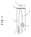
- Fig. 1 shows an example of the structure of the latter optical module.
- a branching waveguide is formed by a PLC.
- An optical fiber 14 is mounted, without being adjusted, on a PLC platform 11 by using a V-groove.
- the optical fiber core and the waveguide 11 a can be positioned at a micrometer level.
- a semiconductor laser 12 and the optical fiber 14 can be coupled to the waveguide at a sub-micrometer level, without the need of optical axis alignment, in such a way that a mark pattern formed on the semiconductor laser 12 and a mark pattern formed on the PLC platform 11 are matched with each other by using infrared transmitted light.
- optical module configured in this way, all the work of optical axis alignment can be automated. This greatly contributes to reducing the production cost of the optical module.
- the optical module is configured such that an optical filter 15 is arranged at a returning portion of the waveguide 11a, and that only light of a specific wavelength is returned at the returning portion and light of the other wavelengths is received by a PD 16 supported by a PD carrier I7.
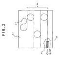
- a wavelength tunable laser As a device in which the passive alignment is used, there is a wavelength tunable laser as shown in Fig. 2 .
- This device is regarded as a key device of the WDM transmission system and is energetically studied in many research institutes.
- three stages of ring resonators 24 are connected in series on a PLC platform 21, and the waveguide is configured to be turned back by a waveguide mirror 25.
- a wavelength tunable operation is realized by performing phase control in such a way that the refractive index is locally changed by energizing a heater formed in the each ring resonator.
- One of the ring resonators is adjusted to match a predetermined period (for example, a period of ITU grid), so that a highly precise wavelength locking operation is realized.
- Japanese Patent Laid Open Publication No. 2001-272582 there is disclosed an invention in which a structure configured to make the end of an adhesive layer recede to the inside from a light emitting surface is adopted, and in which it is thereby prevented that the end of the adhesive layer is extended to be raised to the emitting surface side and projects in the optical path so as to shield the emitted light.
- the viscosity of the refractive index matching gel is generally low.
- the gel is spread over a wide area. Therefore, in the case where the refractive index matching gel is used, even when the end of the coating area is set to the inside of the light emitting surface as in the invention disclosed in Japanese Patent Laid Open Publication No. 2001-272582 , a part of the gel may be turned to reach the light emitting surface, so as to thereby prevent the light emission. That is, a part of gels may also be turned to reach the light emitting section of the SOA with phase control. In this case, there is a possibility that the front surface reflectance is made lower than a design value, or that the efficiency of coupling with the optical fiber is lowered by deformation of the light emitting surface.
- the turning of the refractive index matching gel causes a characteristic change and causes to lower the yield.
- An exemplary object of the present invention is to provide a mounting structure of a semiconductor optical element, in which structure the turning of the refractive index matching gel is prevented.
- a mounting structure of a semiconductor optical element in which structure signal light emitted from one end of the semiconductor optical element mounted to a platform with an optical waveguide formed therein is made incident on the optical waveguide and is then again made incident on the semiconductor optical element to be emitted from the other end of the semiconductor optical element, wherein the semiconductor optical element is mounted to the platform in a state where the other end is projected from the platform, and wherein a refractive index matching gel is arranged between the one end of the semiconductor optical element and the optical waveguide.
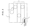
- Fig. 3 and Fig. 4 show a mounting structure of a semiconductor optical element according to the present embodiment.
- An SOA 2 with phase control is mounted on a PLC platform 1 by the passive alignment.
- the passive alignment technique is a technique in which the positioning is performed by using a mark pattern formed on the PLC substrate surface and a mark pattern of an LD chip, and which eliminates the need of optical axis alignment previously performed in manufacturing an optical module and greatly improves the cost and the lead time for producing the module.
- pedestals 6 are arranged between the SOA 2 with phase control and the PLC platform 1.
- the waveguide 1a coupled to the SOA 2 with phase control, three stages of ring resonators 4 are formed. Further, the waveguide 1a is configured to be turned back by a waveguide mirror 5, so that a wavelength tunable operation is performed.
- the end surface of the SOA 2 with phase control mounted by the passive alignment is projected from the end surface of the PLC platform 1.
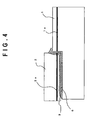
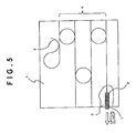
- Fig. 5 shows a configuration of a modulator integrated wavelength tunable laser in the case where a modulator 7 is mounted as another chip by the passive alignment in addition to the SOA 2 with phase control.
- the configuration of the second exemplary embodiment is almost the same as that of the first exemplary embodiment, but is different in that the modulator 7 is further provided.
- the oscillation characteristics can be more stabilized as the reflectance of the emitting end of the modulator 7 is reduced. For this reason, when the refractive index matching gel 3 is brought into contact with the emitting end surface of the modulator 7, the reflectance of the emitting end of the modulator is increased, so that the oscillating operation of the wavelength tunable laser is made unstable. In addition, the coupling characteristics with the fiber may be deteriorated by the deformation of the emitting end surface.
- the end surface of the light taking-out modulator 7 is projected from the PLC platform 1. This prevents the refractive index matching gel 3 from being brought into contact with the emitting end surface of the modulator 7, so that the stable operation and the excellent coupling characteristics with the fiber can be realized.
- the each embodiment as described above is configured such that the wavelength tunable operation is performed by using the three stages of ring resonators, but the number of stages of ring resonators can be arbitrarily set. Further, as long as the wavelength tunable operation can be performed, the ring resonator need not be necessarily used.
- each embodiment as described above is configured such that the SOA with phase control is used as an example of a semiconductor optical element.
- the present invention can be applied to all semiconductor optical elements including a semiconductor laser.
- An example 1 is a mounting structure of a semiconductor optical element, in which structure signal light emitted from one end of the semiconductor optical element mounted to a platform with an optical waveguide formed therein is made incident on the optical waveguide and is then again made incident on the semiconductor optical element to be emitted from the other end of the semiconductor optical element, wherein the semiconductor optical element is mounted to the platform in a state where the other end is projected from the platform, and wherein a refractive index matching gel is arranged between the one end of the semiconductor optical element and the optical waveguide.
- An example 2 is the mounting structure of the semiconductor optical element according to example 1, wherein the signal light turned back by a mirror formed at the end of the optical waveguide is again made incident on the semiconductor optical element.
- An example 3 is the mounting structure of the semiconductor optical element according to one of example 1 or 2, wherein a wavelength tunable circuit is formed in the platform by the optical waveguide.
- An example 4 is the mounting structure of the semiconductor optical element according to example 3, wherein the wavelength tunable circuit comprises at least one stage of a ring resonator.
- An example 5 is the mounting structure of the semiconductor optical element according to any one of examples 1 to 4, wherein a refractive index of the refractive index matching gel is set closer to a refractive index of the optical waveguide than to a refractive index of the semiconductor optical element.
- An example 6 is the mounting structure of the semiconductor optical element according to any one of examples 1 to 5, wherein the semiconductor optical element is a semiconductor optical amplifier with phase control.
- An example 7 is the mounting structure of the semiconductor optical element according to any one of examples 1 to 5, wherein the semiconductor optical element includes a semiconductor optical amplifier with phase control arranged on the side of the one end and coupled to the optical waveguide, and a modulator arranged on the side of the other end and configured to modulate the light signal again made incident.
- the semiconductor optical element includes a semiconductor optical amplifier with phase control arranged on the side of the one end and coupled to the optical waveguide, and a modulator arranged on the side of the other end and configured to modulate the light signal again made incident.
Landscapes
- Physics & Mathematics (AREA)
- General Physics & Mathematics (AREA)
- Optics & Photonics (AREA)
- Semiconductor Lasers (AREA)
- Optical Couplings Of Light Guides (AREA)
- Optical Integrated Circuits (AREA)
Claims (7)
- Aufbaustruktur eines optischen Halbleiterelements, in der Struktursignallicht, das von einem Ende des optischen Halbleiterelements (2) emittiert wird, das auf einer Plattform (1) mit einem darin ausgebildeten optischen Wellenleiter (1a) angeordnet ist, auf den optischen Wellenleiter (1a) einfallend und dann erneut auf das optische Halbleiterelement (2) einfallend geführt wird, so dass es vom anderen Ende des optischen Halbleiterelements (2) emittiert wird,
dadurch gekennzeichnet, dass das optische Halbleiterelement (2) derart auf der Plattform (1) angeordnet ist, dass das andere Ende von der Plattform (1) vorsteht, und
wobei zwischen dem einen Ende des optischen Halbleiterelements (2) und dem optischen Wellenleiter (1a) ein Gel (3) mit angepasstem Brechungsindex angeordnet ist. - Aufbaustruktur eines optischen Halbleiterelements nach Anspruch 1, wobei das Signallicht, das durch einen am Ende des optischen Wellenleiters (1a) ausgebildeten Spiegel (5) zurückgeführt wird, erneut auf das optische Halbleiterelement (2) einfallend geführt wird.
- Aufbaustruktur des optischen Halbleiterelements nach Anspruch 1 oder 2, wobei in der Plattform durch den optischen Wellenleiter ein Wellenlängen-Abstimmschaltkreis ausgebildet ist.
- Aufbaustruktur des optischen Halbleiterelements nach Anspruch 3, wobei der Wellenlängen-Abstimmschaltkreis mindestens eine Stufe eines Ringresonators (4) aufweist.
- Aufbaustruktur des optischen Halbleiterelements nach einem der Ansprüche 1 bis 4, wobei der Brechungsindex des Gels (3) mit angepasstem Brechungsindex näher auf einen Brechungsindex des optischen Wellenleiters (1a) als auf einen Brechungsindex des optischen Halbleiterelements (2) eingestellt ist.
- Aufbaustruktur des optischen Halbleiterelements nach einem der Ansprüche 1 bis 5, wobei das optische Halbleiterelement ein optischer Halbleiterverstärker (2) mit Phasensteuerung ist.
- Aufbaustruktur des optischen Halbleiterelements nach einem der Ansprüche 1 bis 5, wobei das optische Halbleiterelement einen optischen Halbleiterverstärker (2) mit Phasensteuerung, der an der Seite des einen Endes angeordnet und mit dem optischen Wellenleiter (1a) gekoppelt ist, sowie einen Modulator aufweist, der an der Seite des anderen Endes angeordnet und konfiguriert ist, das erneut einfallend geführte Lichtsignal zu modulieren.
Applications Claiming Priority (1)
| Application Number | Priority Date | Filing Date | Title |
|---|---|---|---|
| JP2007177139A JP2009016594A (ja) | 2007-07-05 | 2007-07-05 | 半導体光素子の実装構造 |
Publications (3)
| Publication Number | Publication Date |
|---|---|
| EP2012151A2 EP2012151A2 (de) | 2009-01-07 |
| EP2012151A3 EP2012151A3 (de) | 2009-10-21 |
| EP2012151B1 true EP2012151B1 (de) | 2013-03-06 |
Family
ID=39816913
Family Applications (1)
| Application Number | Title | Priority Date | Filing Date |
|---|---|---|---|
| EP08158119A Expired - Fee Related EP2012151B1 (de) | 2007-07-05 | 2008-06-12 | Montierstruktur eines optischen Halbleiterelements |
Country Status (6)
| Country | Link |
|---|---|
| US (1) | US7539370B2 (de) |
| EP (1) | EP2012151B1 (de) |
| JP (1) | JP2009016594A (de) |
| CN (1) | CN101339278B (de) |
| AU (1) | AU2008202724A1 (de) |
| CA (1) | CA2636094C (de) |
Families Citing this family (8)
| Publication number | Priority date | Publication date | Assignee | Title |
|---|---|---|---|---|
| KR101405419B1 (ko) * | 2010-06-18 | 2014-06-27 | 한국전자통신연구원 | 레이저 모듈 |
| JP5708009B2 (ja) | 2011-02-17 | 2015-04-30 | セイコーエプソン株式会社 | 光モジュールおよび電子機器 |
| JP2012256667A (ja) * | 2011-06-08 | 2012-12-27 | Nippon Telegr & Teleph Corp <Ntt> | 半導体レーザ光源 |
| JPWO2014118836A1 (ja) * | 2013-02-01 | 2017-01-26 | 日本電気株式会社 | 光機能集積ユニット及びその製造方法 |
| US9787054B2 (en) * | 2015-05-05 | 2017-10-10 | Sifotonics Technologies Co., Ltd. | Optical package providing efficient coupling between DFB-LD and silicon PIC edge couplers with low return loss |
| CN107065082B (zh) * | 2016-02-01 | 2019-03-05 | 硅光电科技股份有限公司 | 带有边缘耦合器的硅光子低回波损耗封装结构 |
| US10234701B2 (en) * | 2016-10-18 | 2019-03-19 | Morton Photonics | Waveguide array modulator for high performance systems |
| JP7211017B2 (ja) | 2018-11-02 | 2023-01-24 | 株式会社デンソー | 光フィルタ、それを用いたレーザ光源および光送受信装置 |
Family Cites Families (17)
| Publication number | Priority date | Publication date | Assignee | Title |
|---|---|---|---|---|
| JPS5870592A (ja) * | 1981-10-23 | 1983-04-27 | Hitachi Ltd | レ−ザ−ダイオ−ド |
| US4611884A (en) * | 1982-11-24 | 1986-09-16 | Magnetic Controls Company | Bi-directional optical fiber coupler |
| JPS6063981A (ja) * | 1984-07-27 | 1985-04-12 | Hitachi Ltd | 半導体発光装置 |
| JPS6360578A (ja) * | 1986-09-01 | 1988-03-16 | Sumitomo Electric Ind Ltd | 固体レ−ザ素子 |
| JPH0731314B2 (ja) * | 1987-06-30 | 1995-04-10 | 日本電気株式会社 | 光信号の変調装置 |
| JP2001024268A (ja) * | 1999-07-05 | 2001-01-26 | Matsushita Electric Ind Co Ltd | 半導体レーザ装置 |
| JP3990113B2 (ja) | 2000-01-19 | 2007-10-10 | 日本オプネクスト株式会社 | 光電子装置及びその製造方法 |
| US6476379B2 (en) * | 2000-01-19 | 2002-11-05 | Hitachi, Ltd. | Optoelectronic devices and manufacturing method thereof |
| JP2001330762A (ja) * | 2000-05-24 | 2001-11-30 | Oki Electric Ind Co Ltd | 光モジュール |
| US6907054B2 (en) * | 2001-06-29 | 2005-06-14 | Sharp Kabushiki Kaisha | Semiconductor laser device |
| US6810058B2 (en) * | 2002-04-23 | 2004-10-26 | Adc Telecommunications, Inc. | Semiconductor laser with gain waveguide layer providing transversal and longitudinal mode stability |
| US20040208458A1 (en) * | 2002-11-26 | 2004-10-21 | Hitoshi Uno | Bidirectional optical module, optical drop module, and optical transmission device |
| US20040223712A1 (en) * | 2003-04-28 | 2004-11-11 | Ruolin Li | Technique for stabilizing laser wavelength and phase |
| JP2006278769A (ja) * | 2005-03-29 | 2006-10-12 | Nec Corp | 波長可変レーザ |
| JP2007133011A (ja) * | 2005-11-08 | 2007-05-31 | Nec Corp | 光結合構造およびその製造方法、光モジュール |
| JP2007171488A (ja) * | 2005-12-21 | 2007-07-05 | Fuji Xerox Co Ltd | 双方向通信用光導波路及び光送受信器 |
| JP5078256B2 (ja) | 2005-12-28 | 2012-11-21 | 株式会社ブリヂストン | 変性共役ジエン系重合体を用いたゴム組成物及び空気入りタイヤ |
-
2007
- 2007-07-05 JP JP2007177139A patent/JP2009016594A/ja active Pending
-
2008
- 2008-06-12 EP EP08158119A patent/EP2012151B1/de not_active Expired - Fee Related
- 2008-06-20 AU AU2008202724A patent/AU2008202724A1/en not_active Abandoned
- 2008-06-24 US US12/145,064 patent/US7539370B2/en active Active
- 2008-06-25 CA CA2636094A patent/CA2636094C/en not_active Expired - Fee Related
- 2008-07-07 CN CN200810135605.6A patent/CN101339278B/zh active Active
Also Published As
| Publication number | Publication date |
|---|---|
| AU2008202724A1 (en) | 2009-01-22 |
| EP2012151A2 (de) | 2009-01-07 |
| US20090010592A1 (en) | 2009-01-08 |
| CA2636094C (en) | 2012-10-02 |
| CA2636094A1 (en) | 2009-01-05 |
| US7539370B2 (en) | 2009-05-26 |
| CN101339278A (zh) | 2009-01-07 |
| JP2009016594A (ja) | 2009-01-22 |
| CN101339278B (zh) | 2012-05-30 |
| EP2012151A3 (de) | 2009-10-21 |
Similar Documents
| Publication | Publication Date | Title |
|---|---|---|
| EP2012151B1 (de) | Montierstruktur eines optischen Halbleiterelements | |
| US11086078B2 (en) | Methods and system for wavelength tunable optical components and sub-systems | |
| US7843986B2 (en) | Planar lightwave circuit and tunable laser device having the same | |
| US8145017B2 (en) | Optical module | |
| US7539369B2 (en) | Optical device and manufacturing method thereof | |
| US8885675B2 (en) | Wavelength variable laser device, and method and program for controlling the same | |
| US7440643B2 (en) | Variable light controlling device and variable light controlling method | |
| US8643943B2 (en) | Tunable laser source using intracavity laser light outcoupling and module containing the same | |
| US20090135861A1 (en) | Soi-based tunable laser | |
| US20010053265A1 (en) | Optical device for use in detecting the wavelength and intensity of light | |
| CN104937790A (zh) | 光学功能集成单元及其制造方法 | |
| US20160261092A1 (en) | Temperature insensitive laser | |
| EP1008211A1 (de) | Integrierter multiwellenlängensender | |
| US20190324201A1 (en) | Optical transposer assembly | |
| EP4500249A1 (de) | Verfahren zur integration eines wellenlängenverrieglers und prozesse zur nutzung gedruckter photonischer strukturen | |
| JP2005004204A (ja) | 光ハイブリッドモジュール及びその製造方法 | |
| Zhao et al. | Integrated Filtered-Feedback Multi-Wavelength Laser | |
| US20090268762A1 (en) | Optical intergrated device | |
| Wang et al. | Optics in Computer Architectures: Basis of WDM, Technologies and Potentials | |
| WO2009054808A1 (en) | Packaged tunable semiconductor laser structure and its fabrication | |
| Kitamura | PLC based bi-directional optical module for access fiber networks |
Legal Events
| Date | Code | Title | Description |
|---|---|---|---|
| PUAI | Public reference made under article 153(3) epc to a published international application that has entered the european phase |
Free format text: ORIGINAL CODE: 0009012 |
|
| AK | Designated contracting states |
Kind code of ref document: A2 Designated state(s): AT BE BG CH CY CZ DE DK EE ES FI FR GB GR HR HU IE IS IT LI LT LU LV MC MT NL NO PL PT RO SE SI SK TR |
|
| AX | Request for extension of the european patent |
Extension state: AL BA MK RS |
|
| PUAL | Search report despatched |
Free format text: ORIGINAL CODE: 0009013 |
|
| AK | Designated contracting states |
Kind code of ref document: A3 Designated state(s): AT BE BG CH CY CZ DE DK EE ES FI FR GB GR HR HU IE IS IT LI LT LU LV MC MT NL NO PL PT RO SE SI SK TR |
|
| AX | Request for extension of the european patent |
Extension state: AL BA MK RS |
|
| 17P | Request for examination filed |
Effective date: 20100331 |
|
| 17Q | First examination report despatched |
Effective date: 20100506 |
|
| AKX | Designation fees paid |
Designated state(s): DE FR GB |
|
| GRAP | Despatch of communication of intention to grant a patent |
Free format text: ORIGINAL CODE: EPIDOSNIGR1 |
|
| GRAS | Grant fee paid |
Free format text: ORIGINAL CODE: EPIDOSNIGR3 |
|
| GRAA | (expected) grant |
Free format text: ORIGINAL CODE: 0009210 |
|
| RIN1 | Information on inventor provided before grant (corrected) |
Inventor name: YAMAZAKI, HIROYUKI |
|
| AK | Designated contracting states |
Kind code of ref document: B1 Designated state(s): DE FR GB |
|
| REG | Reference to a national code |
Ref country code: GB Ref legal event code: FG4D |
|
| REG | Reference to a national code |
Ref country code: DE Ref legal event code: R096 Ref document number: 602008022655 Country of ref document: DE Effective date: 20130502 |
|
| PGFP | Annual fee paid to national office [announced via postgrant information from national office to epo] |
Ref country code: GB Payment date: 20130415 Year of fee payment: 6 |
|
| PGFP | Annual fee paid to national office [announced via postgrant information from national office to epo] |
Ref country code: DE Payment date: 20130731 Year of fee payment: 6 |
|
| PGFP | Annual fee paid to national office [announced via postgrant information from national office to epo] |
Ref country code: FR Payment date: 20130726 Year of fee payment: 6 |
|
| PLBE | No opposition filed within time limit |
Free format text: ORIGINAL CODE: 0009261 |
|
| STAA | Information on the status of an ep patent application or granted ep patent |
Free format text: STATUS: NO OPPOSITION FILED WITHIN TIME LIMIT |
|
| 26N | No opposition filed |
Effective date: 20131209 |
|
| REG | Reference to a national code |
Ref country code: DE Ref legal event code: R097 Ref document number: 602008022655 Country of ref document: DE Effective date: 20131209 |
|
| REG | Reference to a national code |
Ref country code: DE Ref legal event code: R119 Ref document number: 602008022655 Country of ref document: DE |
|
| GBPC | Gb: european patent ceased through non-payment of renewal fee |
Effective date: 20140612 |
|
| REG | Reference to a national code |
Ref country code: FR Ref legal event code: ST Effective date: 20150227 |
|
| REG | Reference to a national code |
Ref country code: DE Ref legal event code: R119 Ref document number: 602008022655 Country of ref document: DE Effective date: 20150101 |
|
| PG25 | Lapsed in a contracting state [announced via postgrant information from national office to epo] |
Ref country code: DE Free format text: LAPSE BECAUSE OF NON-PAYMENT OF DUE FEES Effective date: 20150101 |
|
| PG25 | Lapsed in a contracting state [announced via postgrant information from national office to epo] |
Ref country code: GB Free format text: LAPSE BECAUSE OF NON-PAYMENT OF DUE FEES Effective date: 20140612 Ref country code: FR Free format text: LAPSE BECAUSE OF NON-PAYMENT OF DUE FEES Effective date: 20140630 |