EP2011153B1 - Optoelectronic display and method of manufacturing the same - Google Patents
Optoelectronic display and method of manufacturing the same Download PDFInfo
- Publication number
- EP2011153B1 EP2011153B1 EP07732312A EP07732312A EP2011153B1 EP 2011153 B1 EP2011153 B1 EP 2011153B1 EP 07732312 A EP07732312 A EP 07732312A EP 07732312 A EP07732312 A EP 07732312A EP 2011153 B1 EP2011153 B1 EP 2011153B1
- Authority
- EP
- European Patent Office
- Prior art keywords
- sub
- layer
- colour
- light
- emissive
- Prior art date
- Legal status (The legal status is an assumption and is not a legal conclusion. Google has not performed a legal analysis and makes no representation as to the accuracy of the status listed.)
- Not-in-force
Links
Images


Classifications
-
- G—PHYSICS
- G09—EDUCATION; CRYPTOGRAPHY; DISPLAY; ADVERTISING; SEALS
- G09F—DISPLAYING; ADVERTISING; SIGNS; LABELS OR NAME-PLATES; SEALS
- G09F9/00—Indicating arrangements for variable information in which the information is built-up on a support by selection or combination of individual elements
- G09F9/30—Indicating arrangements for variable information in which the information is built-up on a support by selection or combination of individual elements in which the desired character or characters are formed by combining individual elements
- G09F9/302—Indicating arrangements for variable information in which the information is built-up on a support by selection or combination of individual elements in which the desired character or characters are formed by combining individual elements characterised by the form or geometrical disposition of the individual elements
-
- G—PHYSICS
- G09—EDUCATION; CRYPTOGRAPHY; DISPLAY; ADVERTISING; SEALS
- G09G—ARRANGEMENTS OR CIRCUITS FOR CONTROL OF INDICATING DEVICES USING STATIC MEANS TO PRESENT VARIABLE INFORMATION
- G09G3/00—Control arrangements or circuits, of interest only in connection with visual indicators other than cathode-ray tubes
- G09G3/20—Control arrangements or circuits, of interest only in connection with visual indicators other than cathode-ray tubes for presentation of an assembly of a number of characters, e.g. a page, by composing the assembly by combination of individual elements arranged in a matrix no fixed position being assigned to or needed to be assigned to the individual characters or partial characters
- G09G3/22—Control arrangements or circuits, of interest only in connection with visual indicators other than cathode-ray tubes for presentation of an assembly of a number of characters, e.g. a page, by composing the assembly by combination of individual elements arranged in a matrix no fixed position being assigned to or needed to be assigned to the individual characters or partial characters using controlled light sources
- G09G3/30—Control arrangements or circuits, of interest only in connection with visual indicators other than cathode-ray tubes for presentation of an assembly of a number of characters, e.g. a page, by composing the assembly by combination of individual elements arranged in a matrix no fixed position being assigned to or needed to be assigned to the individual characters or partial characters using controlled light sources using electroluminescent panels
- G09G3/32—Control arrangements or circuits, of interest only in connection with visual indicators other than cathode-ray tubes for presentation of an assembly of a number of characters, e.g. a page, by composing the assembly by combination of individual elements arranged in a matrix no fixed position being assigned to or needed to be assigned to the individual characters or partial characters using controlled light sources using electroluminescent panels semiconductive, e.g. using light-emitting diodes [LED]
- G09G3/3208—Control arrangements or circuits, of interest only in connection with visual indicators other than cathode-ray tubes for presentation of an assembly of a number of characters, e.g. a page, by composing the assembly by combination of individual elements arranged in a matrix no fixed position being assigned to or needed to be assigned to the individual characters or partial characters using controlled light sources using electroluminescent panels semiconductive, e.g. using light-emitting diodes [LED] organic, e.g. using organic light-emitting diodes [OLED]
-
- G—PHYSICS
- G09—EDUCATION; CRYPTOGRAPHY; DISPLAY; ADVERTISING; SEALS
- G09G—ARRANGEMENTS OR CIRCUITS FOR CONTROL OF INDICATING DEVICES USING STATIC MEANS TO PRESENT VARIABLE INFORMATION
- G09G3/00—Control arrangements or circuits, of interest only in connection with visual indicators other than cathode-ray tubes
- G09G3/20—Control arrangements or circuits, of interest only in connection with visual indicators other than cathode-ray tubes for presentation of an assembly of a number of characters, e.g. a page, by composing the assembly by combination of individual elements arranged in a matrix no fixed position being assigned to or needed to be assigned to the individual characters or partial characters
- G09G3/34—Control arrangements or circuits, of interest only in connection with visual indicators other than cathode-ray tubes for presentation of an assembly of a number of characters, e.g. a page, by composing the assembly by combination of individual elements arranged in a matrix no fixed position being assigned to or needed to be assigned to the individual characters or partial characters by control of light from an independent source
- G09G3/36—Control arrangements or circuits, of interest only in connection with visual indicators other than cathode-ray tubes for presentation of an assembly of a number of characters, e.g. a page, by composing the assembly by combination of individual elements arranged in a matrix no fixed position being assigned to or needed to be assigned to the individual characters or partial characters by control of light from an independent source using liquid crystals
- G09G3/3607—Control arrangements or circuits, of interest only in connection with visual indicators other than cathode-ray tubes for presentation of an assembly of a number of characters, e.g. a page, by composing the assembly by combination of individual elements arranged in a matrix no fixed position being assigned to or needed to be assigned to the individual characters or partial characters by control of light from an independent source using liquid crystals for displaying colours or for displaying grey scales with a specific pixel layout, e.g. using sub-pixels
-
- H—ELECTRICITY
- H10—SEMICONDUCTOR DEVICES; ELECTRIC SOLID-STATE DEVICES NOT OTHERWISE PROVIDED FOR
- H10K—ORGANIC ELECTRIC SOLID-STATE DEVICES
- H10K59/00—Integrated devices, or assemblies of multiple devices, comprising at least one organic light-emitting element covered by group H10K50/00
- H10K59/30—Devices specially adapted for multicolour light emission
- H10K59/35—Devices specially adapted for multicolour light emission comprising red-green-blue [RGB] subpixels
- H10K59/352—Devices specially adapted for multicolour light emission comprising red-green-blue [RGB] subpixels the areas of the RGB subpixels being different
-
- H—ELECTRICITY
- H10—SEMICONDUCTOR DEVICES; ELECTRIC SOLID-STATE DEVICES NOT OTHERWISE PROVIDED FOR
- H10K—ORGANIC ELECTRIC SOLID-STATE DEVICES
- H10K59/00—Integrated devices, or assemblies of multiple devices, comprising at least one organic light-emitting element covered by group H10K50/00
- H10K59/30—Devices specially adapted for multicolour light emission
- H10K59/35—Devices specially adapted for multicolour light emission comprising red-green-blue [RGB] subpixels
- H10K59/353—Devices specially adapted for multicolour light emission comprising red-green-blue [RGB] subpixels characterised by the geometrical arrangement of the RGB subpixels
-
- G—PHYSICS
- G09—EDUCATION; CRYPTOGRAPHY; DISPLAY; ADVERTISING; SEALS
- G09G—ARRANGEMENTS OR CIRCUITS FOR CONTROL OF INDICATING DEVICES USING STATIC MEANS TO PRESENT VARIABLE INFORMATION
- G09G2300/00—Aspects of the constitution of display devices
- G09G2300/04—Structural and physical details of display devices
- G09G2300/0439—Pixel structures
- G09G2300/0452—Details of colour pixel setup, e.g. pixel composed of a red, a blue and two green components
-
- H—ELECTRICITY
- H10—SEMICONDUCTOR DEVICES; ELECTRIC SOLID-STATE DEVICES NOT OTHERWISE PROVIDED FOR
- H10K—ORGANIC ELECTRIC SOLID-STATE DEVICES
- H10K50/00—Organic light-emitting devices
- H10K50/80—Constructional details
- H10K50/805—Electrodes
-
- H—ELECTRICITY
- H10—SEMICONDUCTOR DEVICES; ELECTRIC SOLID-STATE DEVICES NOT OTHERWISE PROVIDED FOR
- H10K—ORGANIC ELECTRIC SOLID-STATE DEVICES
- H10K59/00—Integrated devices, or assemblies of multiple devices, comprising at least one organic light-emitting element covered by group H10K50/00
- H10K59/80—Constructional details
- H10K59/805—Electrodes
- H10K59/8051—Anodes
- H10K59/80515—Anodes characterised by their shape
Definitions
- This invention relates to an optoelectronic display and a method of manufacturing the same.
- LCDs Liquid Crystal Displays
- EL ElectroLuminescent
- PDs Plasma Displays
- Multicoloured displays typically comprise a plurality of pixels, each pixel comprising a plurality of sub-pixels.
- the sub-pixels are defined by a colour-forming layer.
- the colour-forming layer may be a light-emissive layer comprising a plurality of discrete light-emissive regions of different light-emissive material defining the sub-pixels.
- an EL display has such a light-emissive layer disposed between electrodes which are patterned so as to be able to address the individual sub-pixels which correspond to the discrete light-emissive regions of the light-emissive layer.
- the colour-forming layer may be a colour filter comprising a plurality of discrete regions of different colour defining the sub-pixels.
- an LCD may have such a filter with a white bacldight and a liquid crystal arrangement for addressing the individual sub-pixels that correspond to the discrete coloured regions of the filter.
- Figure 1 shows a standard pixel arrangement in which each pixel 2 comprises a single red sub-pixel 4, a single green sub-pixel 6 and a single blue sub-pixel 8, all of which are the same size.
- each pixel 2 comprising a central blue sub-pixel 8, with red sub-pixels 4 in one pair of diagonally opposing corners, and green sub-pixels 6 in the other pair of diagonally opposing corners.
- the sub-pixels are arranged so that around a junction between four adjacent pixels, the sub-pixels alternate between red and green.
- a problem with the aforementioned arrangements is that it is difficult to provide an intricately patterned colour-forming layer. Furthermore, depending on the materials and the patterning techniques used, there will be a lower limit to the size of discrete colour-forming regions that can be reliably formed.
- Embodiments of the present invention seek to solve the aforementioned problems in the prior art by providing a pixel/sub-pixel arrangement that is easier to manufacture and has good visual performance.
- EP 1544928 discloses a display device in which a pixel has a plurality of elements of the same colour.
- each pixel is composed of a plurality of subpixel regions corresponding to red, green or blue colours.
- Each of the specific color sub-pixel regions in the pixel device abuts the same specific color sub-pixel region of the adjacent pixel device thereof to form a double-sized area.
- US 2003/160915 discloses a pixel array arrangement for a colour filter. Each pixel array has four sub-pixels and the color of a sub-pixel of the pixel array is identical to that of another sub-pixel of another pixel array adjacent to the pixel array.
- US 2002/047567 discloses an active matrix organic LED display device.
- JP 2000/260573 discloses an organic EL element comprising wires that are embedded in the surface of a transparent substrate so as to make contact with a transparent electrode.
- an optoelectronic display comprising a plurality of pixels, each pixel comprising a plurality of sub-pixels, wherein the optoelectronic display comprises a colour-forming layer which is patterned providing a plurality of discrete colour- forming regions in a two-dimensional array, each colour forming region being a continuous region of colour-forming material and wherein an addressing array is provided for addressing the discrete colour-forming regions, characterized in that the colour forming layer is a light-emitting layer, and at least some of the discrete colour-forming regions have a plurality of portions which are separately addressable by the addressing array, each portion defining a sub-pixel of the optoelectronic display.
- two-dimensional array we mean an array comprising a plurality of point-like discrete colour-forming regions.
- the point-like colour-forming regions may have various shapes including circular, oval, rectangular, square and hexagonal.
- discrete colour forming region we mean a continuous region of colour-forming material rather than a plurality of colour-forming regions.
- continuous region we mean continuous in the plane of the display.
- a discrete colour-forming region may comprise a number of layers, one on top of the other, in a direction perpendicular to the plane of the display. However, if such layers are continuous in the plane of the display then they would constitute a discrete colour-forming region.
- each sub-pixel does not have to be defined by a corresponding discrete colour-forming region.
- At least some of the discrete colour-forming regions provide a plurality of sub-pixels which are individually addressable by the addressing array. This simplifies the patterning process for the colour-forming layer while not significantly reducing visual performance of the display. Furthermore, an increase in resolution can be achieved with no change in the pattern of the colour-forming layer.
- each separately addressable portion defines a sub-pixel of a different pixel in the optoelectronic display.
- the discrete colour-forming regions may have any number of separately addressable portions. However, in preferred arrangements discrete colour forming regions have 2, 3, 4 or 6 separately addressable portions.
- the colour-forming layer is emissive.
- An example is an optoelectronic display which comprises: a substrate; a first electrode layer disposed over the substrate; a light-emissive layer disposed over the first electrode layer; and a second electrode layer disposed over the light-emissive layer.
- the light emissive layer constitutes the colour-forming layer which is patterned providing a plurality of discrete light-emissive regions in a two-dimensional array.
- the electrode layers constitute the addressing array with the first electrode layer and/or the second electrode layer comprising a plurality of electrodes, each electrode comprising at least two sub-electrodes drivably associated with each discrete light-emissive region.
- each discrete light-emissive region allows areas of the discrete light-emissive region to be differentially driven. Accordingly, a discrete light-emissive region can contribute to a plurality of different sub-pixels.
- the display is an active matrix display, each sub-pixel having an active switching component associated therewith in order to provide different drive voltages to each sub-electrode.
- the light-emissive layer is patterned by providing a bank structure disposed over the first electrode layer defining a plurality of wells, each well containing one of the discrete light-emissive regions, whereby at least two of the sub-electrodes are associated with each well.
- the first electrode layer comprises said plurality of electrodes with at least two of the sub-electrodes being associated with each discrete light-emissive region.
- the first electrode is the anode.
- the anode may be any suitable material but is preferably ITO.
- One class of optoelectronic displays is that using an organic material for light emission.
- the basic structure of these devices is a light emissive organic layer, for instance a film of a poly (p-phenylenevinylene) (“PPV”) or polyfluorene, sandwiched between a cathode for injecting negative charge carriers (electrons) and an anode for injecting positive charge carriers (holes) into the organic layer.
- the electrons and holes combine in the organic layer generating photons.
- the organic light- emissive material is a polymer.
- the organic light-emissive material is of the class known as small molecule materials, such as (8-hydroxyquinoline) aluminium (“Alq3"). In a practical device one of the electrodes is transparent, to allow the photons to escape the device,
- a typical organic light-emissive display is fabricated on a glass or plastic substrate coated with a transparent anode such as indium-tin-oxide ("ITO").
- ITO indium-tin-oxide
- a layer of a thin film of at least one electroluminescent organic material covers the first electrode.
- a cathode covers the layer of electroluminescent organic material.
- the cathode is typically a metal or alloy and may comprise a single layer, such as aluminium, or a plurality of layers such as calcium and aluminium.
- holes are injected into the device through the anode and electrons are injected into the device through the cathode.
- the holes and electrons combine in the organic electroluminescent layer to form excitons which then undergo radiative decay to give light (in light detecting devices this process essentially runs in reverse).
- Organic light-emissive displays can provide a particularly advantageous form of electro-optic display. They are bright, stylish, fast-switching, provide a wide viewing angle and are easy and cheap to fabricate on a variety of substrates.
- Organic (which here includes organometallic) light-emissive displays may be fabricated using either polymers or small molecules in a range of colours (or in multi-coloured displays), depending upon the materials used.
- Organic light-emissive displays may be deposited on a substrate in a matrix of pixels to form a single or multi-colour pixellated display.
- a multicoloured display may be constructed using groups of red, green, and blue emitting pixels.
- So-called active matrix displays have a memory element, typically a storage capacitor and a transistor, associated with each pixel whilst passive matrix displays have no such memory element and instead are repetitively scanned to give the impression of a steady image.
- a conductive polymer layer is disposed between the first electrode layer and the light-emissive layer.
- This layer may be any suitable material but is preferably PEDOT-PSS.
- At least one of the conductive polymer layer and the light-emissive layer is deposited by ink jet printing.
- sub-electrodes If the material of the sub-electrodes is of a low enough conductivity so as to make lateral conduction negligible, then no gap need be provided between the sub-electrodes.
- sub-electrodes could be made of a thin layer of material in order to increase lateral resistance and reduce lateral conduction thus negating the requirement for a gap between the sub-electrodes.
- additional conductive connecting lines will usually be required, particularly for a passive matrix display, as otherwise the resistance across the display will generally be too high. This is not such a problem for active matrix displays in which each discrete light-emissive region will have its own driver.
- an ITO anode of typically 150nm thickness is used in standard devices.
- a thinner layer may be used in accordance with embodiments of the present invention in order to avoid lateral conduction between sub-electrodes, e.g. 1 ⁇ 2 or 1 ⁇ 4 of this thickness. In this case, a more conductive connecting line may be provided.
- an ITO anode of this lower thickness can be utilized as the distance between the drivers and the pixels is small.
- the sub-electrodes are connected to a conductive connecting line via a resistive connection which may be provided by, for example, a thin portion of the electrode material.
- a resistive connection which may be provided by, for example, a thin portion of the electrode material.
- a gap may be provided between the sub-electrodes.
- This gap may be filled with an insulating material in order to planarize the upper surface of the anode.
- suitable planarizing, insulating materials include inorganic dielectrics such as silicon dioxide or a organic photoresist. It is advantageous for the planarizing, insulating material to have similar wetting properties to the material of the sub-electrodes for the material deposited thereover. Furthermore, it is advantageous to select a planarizing, insulating material which is not etched away when patterning the bank material.
- the gap between sub-electrodes may be made sufficiently small that the material deposited thereover can span the gap. If the electrode layer is thin then there is less or no need to planarize the layer.
- the electrode layer prefferably has a constant thickness in order to prevent non-uniformities' in the overlying layers.
- the electrode layer comprising the sub-electrodes comprises two layers, a patterned conductive contact layer defining the sub-electrodes with a uniform layer of charge injecting material thereover.
- a patterned metal contact layer may be provided with a uniform layer of ITO deposited thereover.
- the charge injecting material must be of low enough conductance so as to prevent lateral conduction. This may be achieved, for example, by providing a relatively thin layer of ITO as the charge injecting layer.
- the electrode layer may be patterned by standard photolithography.
- any patterning techniques can be used including, for example, laser ablation, e-beam ablation, dry etching, and wet etching.
- the patterning method need not be subtractive and direct writing techniques can be employed such as ink jet printing.
- a method of manufacturing a light-emissive display according to the first aspect of the invention wherein the colour-forming layer is deposited from solution, e.g. by ink jet printing.
- the method optionally comprises providing a substrate; depositing a first electrode layer over the substrate; depositing a light-emissive layer as the colour-forming layer over the first electrode layer; and depositing a second electrode layer over the light-emissive layer, wherein the light-emissive layer is patterned providing a two-dimensional array of discrete light-emissive regions, and wherein the first electrode layer and/or the second electrode layer comprises a plurality of electrodes, each electrode comprising at least two sub-electrodes associated with each discrete light-emissive region.
- the light-emissive layer is patterned by depositing a bank structure disposed over the first electrode layer defining a plurality of wells prior to depositing the light-emissive layer, the light-emissive layer being subsequently deposited such that each well contains one of the discrete light-emissive regions, whereby at least two sub-electrodes are associated with each well.
- the sub-electrodes are patterned by laser ablation, e-beam ablation, dry etching, wet etching, or direct writing.
- Ink jet printing is particularly useful due to its scalability and adaptability.
- the former allows arbitrarily large sized substrates to be patterned and the latter should mean that there are negligible tooling costs associated with changing from one product to another since the image of dots printed on a substrate is defined by software.
- the colour-forming layer is deposited by vacuum deposition of small molecules then a shadow mask is typically used to provide the required resolution.
- a shadow mask is typically used to provide the required resolution.
- embodiments of the present invention can provide a higher resolution display without unduly increasing the complexity of the sub-pixels or unduly decreasing their size.
- FIG. 3 shows a vertical cross section through an example of an OLED device 100.
- the structure of the device is somewhat simplified for the purposes of illustration.
- the OLED 100 comprises a substrate 102, typically 0.7 mm or 1.1 mm glass but optionally clear plastic, on which an anode layer 106 is deposited comprising four separately drivable sub-anodes (shown in Figure 4 ).
- the anode layer typically comprises around 150 nm thickness of ITO (indium tin oxide), over which is provided a metal contact layer, typically around 500nm of aluminium, sometimes referred to as anode metal.
- ITO indium tin oxide
- Glass substrates coated with ITO and contact metal may be purchased from Corning, USA.
- the contact metal (and optionally the ITO) is patterned as desired so that it does not obscure the display, by a conventional process of photolithography followed by etching.
- a substantially transparent hole conducting layer 108a is provided over the anode metal, followed by an electroluminescent layer 108b.
- Banks 112 may be formed on the substrate, for example from positive or negative photoresist material, to define wells 114 into which these active organic layers may be selectively deposited, for example by a droplet deposition or inkjet printing technique. The wells thus define light emitting areas or pixels of the display.
- a cathode layer 110 is then applied by, say, physical vapour deposition.
- the cathode layer typically comprises a low work function metal such as calcium or barium covered with a thicker, capping layer of aluminium and optionally including an additional layer immediately adjacent the electroluminescent layer, such as a layer of lithium fluoride, for improved electron energy level matching.
- a low work function metal such as calcium or barium covered with a thicker, capping layer of aluminium and optionally including an additional layer immediately adjacent the electroluminescent layer, such as a layer of lithium fluoride, for improved electron energy level matching.
- Mutual electrical isolation of cathode lines may achieved through the use of cathode separators.
- a number of displays are fabricated on a single substrate and at the end of the fabrication process the substrate is scribed, and the displays separated.
- An encapsulant such as a glass sheet or a metal can is utilized to inhibit oxidation and moisture ingress.
- Organic LEDs of this general type may be fabricated using a range of materials including polymers, dendrimers, and so-called small molecules, to emit over a range of wavelengths at varying drive voltages and efficiencies.
- Examples of polymer-based OLED materials are described in WO90/13148 , WO95/06400 and WO99/48160 ; examples of dendrimer-based materials are described in WO 99/21935 and WO 021067343 ; and examples of small molecule OLED materials are described in US 4,539,507 .
- the aforementioned polymers, dendrimers and small molecules emit light by radiative decay of singlet excitons (fluorescence). However, up to 75% of excitons are triplet excitons which normally undergo non-radiative decay.
- Electroluminescence by radiative decay of triplet excitons is disclosed in, for example, " Very high-efficiency green organic light-emitting devices based on electrophosphorescence" M.A. Baldo, S. Lamansky, P.E. Burrows, M.E. Thompson, and S.R. Forrest Applied Physics Letters, Vol. 75(1) pp.4-6, July 5, 1999 ".
- layers 108 comprise a hole conducting layer 108a and a light emitting polymer (LEP) electroluminescent layer 108b.
- the electroluminescent layer may comprise, for example, around 70nm (dry) thickness of PPV (poly(p-phenylenevinylene)) and the hole conducting layer, which helps match the hole energy levels of the anode layer and of the electroluminescent layer, may comprise a conductive organic material, for example, around 50-200 nm, preferably around 150 nm (dry) thickness of PEDOT:PSS (polystyrene-sulphonate-doped polyethylene-dioxythiophene).
- PPV poly(p-phenylenevinylene)
- PEDOT:PSS polystyrene-sulphonate-doped polyethylene-dioxythiophene
- Figure 4 shows a plan view of the anode 106 comprising four sub-anodes 106a, 106b, 106c, 106d in accordance with an embodiment of the present invention.
- FIG. 5 shows a sub-pixel arrangement according to an embodiment of the present invention which utilizes electrodes of the type shown in figure 4 .
- Each pixel 50 comprises a central blue sub-pixel 52, with red sub-pixels 54 in one pair of diagonally opposing corners, and green sub-pixels 56 in the other pair of diagonally opposing corners as in the prior art arrangement shown in Figure 2 .
- the sub-pixels at a junction between four adjacent pixels are the same colour and are formed by a single discrete colour-forming region 58.
- the discrete colour-forming region 58 has four separately addressable portions, each portion contributing a sub-pixel to one of the four pixels shown. The portions are separately addressable by utilizing an electrode of the type shown in Figure 4 having four sub-electrodes.
- the relative sizes and shape of the discrete colour-forming regions can be varied.
- organic light-emissive materials it is often the case that the lifetime of the blue emissive material is the limiting factor on the lifetime of the device.
- the blue colour-forming regions By providing the blue colour-forming regions with a larger area, they can be driven at a lower voltage thus increasing the lifetime of the blue colour-forming material in the device.
- any of the blue, green and/or red colour-forming regions may have different sizes according to the performance characteristics of the materials and the desired performance characteristics of the display.
- Figure 6 shows a similar arrangement to that of Figure 5 which utilizes round discrete colour-forming regions rather than square. This arrangement may have a lower aperture ratio than that of Figure 5 but it is advantageous in that the round colour forming regions are more readily ink jet printed.
- the discrete colour-forming region 58 has four portions which are separately addressable by utilizing an electrode similar to that shown in Figure 4 but circular in shape having four segments.
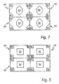
- Figure 7 shows a similar arrangement to that of Figure 5 which utilizes hexagonal discrete colour-forming regions rather than square. This arrangement provides a good aperture ratio while having corners that have a greater angle than in the square arrangement such that ink can readily wet the whole of each discrete colour-forming region.
- Figure 8 shows a similar arrangement to that of Figure 5 but with the square discrete colour-forming regions in a slightly different orientation.
- Figure 9 shows a similar arrangement to that of Figure 5 but with the central sub-pixels of adjacent pixels being merged into a continuous strip.
- Figure 10 shows an arrangement similar to that of Figure 9 but with circular discrete-colour forming regions disposed between the continuous strips, the circular regions having two portions which are individually addressable by utilizing an electrode similar to that shown in Figure 4 but circular in shape having two segments.
- Figure 11 shows an arrangement in which all the discrete colour-forming regions comprise two portions that are individually addressable.
- Figure 12 shows an arrangement which further comprises white colour-forming regions 58.
- Figure 13 shows a similar arrangement to that illustrated in Figure 11 but further including white colour-forming regions 58.
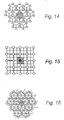
- the previously illustrated arrangements comprise square pixels.
- the pixels may, for example, have a hexagonal, square or triangular shape as shown in Figures 14 to 16 .
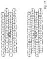
- Figure 17 shows two further arrangements in which the discrete light-emissive regions are substantially rectangular or square and the pixels are substantially triangular. These arrangements may have the most pixels per discrete light-emissive region for a "square-tile" type arrangement.
- the top layout is optimised for a smooth macro-pixel outline. However, in this arrangement the centroids of the macro-pixels do not lie exactly on the square tile points of the square-tile arrangement.
- the bottom layout does not have a smooth macro-pixel outline. However, in this arrangement the centroids of the macro-pixels lie on the square tile points.
- Other considerations include the area of ink lost to drying effects, and in this case the top layout is more immune to these effects as each sub-pixel has approximately the same proportion of well edge and well centre area.
- the resolution of the display is increased without changing the pattern of the colour-forming layer.
- the resolution has been increased by a factor of 3, 4 and 6 respectively with no change in the pattern of the colour-forming layer when compared with analogous arrangements in which the discrete colour-forming regions do not comprise individually addressable portions.
- the arrangements provide enhanced resolution and may be most effective where pixel sizes are on the edge of the eye's spatial resolution.
- blocks of primary colours on a screen may appear dithered as, in effect, with this technique there are clusters of one sub-pixel colour rather than an even distribution.
- the resolution of the eye to luminance variation is twice that of its red-green colour resolution, which is itself twice the blue-yellow colour resolution.
- This technique could also be utilized to achieve the increased resolution required for 3D displays without requiring smaller ink-wells.
- 3-D displays where different macro-pixels are projected in different directions to produce multiple views, it could be arranged such that only similar sub-pixel groupings are projected in any given direction thus removing the visual effect of sub-pixels clustering.
Landscapes
- Engineering & Computer Science (AREA)
- Physics & Mathematics (AREA)
- General Physics & Mathematics (AREA)
- Theoretical Computer Science (AREA)
- Computer Hardware Design (AREA)
- Chemical & Material Sciences (AREA)
- Crystallography & Structural Chemistry (AREA)
- Electroluminescent Light Sources (AREA)
- Devices For Indicating Variable Information By Combining Individual Elements (AREA)
Applications Claiming Priority (2)
| Application Number | Priority Date | Filing Date | Title |
|---|---|---|---|
| GB0607369A GB2437110B (en) | 2006-04-12 | 2006-04-12 | Optoelectronic display and method of manufacturing the same |
| PCT/GB2007/001268 WO2007128971A2 (en) | 2006-04-12 | 2007-04-05 | Optoelectronic display and method of manufacturing the same |
Publications (2)
| Publication Number | Publication Date |
|---|---|
| EP2011153A2 EP2011153A2 (en) | 2009-01-07 |
| EP2011153B1 true EP2011153B1 (en) | 2012-06-13 |
Family
ID=36571708
Family Applications (1)
| Application Number | Title | Priority Date | Filing Date |
|---|---|---|---|
| EP07732312A Not-in-force EP2011153B1 (en) | 2006-04-12 | 2007-04-05 | Optoelectronic display and method of manufacturing the same |
Country Status (7)
| Country | Link |
|---|---|
| US (1) | US8115216B2 (https=) |
| EP (1) | EP2011153B1 (https=) |
| JP (1) | JP5175837B2 (https=) |
| KR (1) | KR101347995B1 (https=) |
| CN (1) | CN101449382B (https=) |
| GB (1) | GB2437110B (https=) |
| WO (1) | WO2007128971A2 (https=) |
Families Citing this family (112)
| Publication number | Priority date | Publication date | Assignee | Title |
|---|---|---|---|---|
| GB2437113B (en) * | 2006-04-12 | 2008-11-26 | Cambridge Display Tech Ltd | Light-emissive display and method of manufacturing the same |
| GB0618698D0 (en) * | 2006-09-22 | 2006-11-01 | Cambridge Display Tech Ltd | Molecular electronic device fabrication methods and structures |
| JP4650495B2 (ja) | 2008-02-05 | 2011-03-16 | セイコーエプソン株式会社 | 発光装置及び電子機器 |
| KR101354329B1 (ko) * | 2009-04-17 | 2014-01-22 | 엘지디스플레이 주식회사 | 영상표시장치 |
| KR101097343B1 (ko) * | 2010-03-09 | 2011-12-23 | 삼성모바일디스플레이주식회사 | 유기 발광 표시 장치 |
| JP5679161B2 (ja) * | 2010-07-23 | 2015-03-04 | 株式会社ジャパンディスプレイ | 有機エレクトロルミネッセンス表示装置 |
| US8835903B2 (en) * | 2010-07-29 | 2014-09-16 | National Tsing Hua University | Light-emitting diode display and method of producing the same |
| JP5536220B2 (ja) * | 2010-09-11 | 2014-07-02 | 三菱電機株式会社 | 有機elパネル |
| US20120120084A1 (en) * | 2010-11-12 | 2012-05-17 | Himax Display, Inc. | Color filter arrangement for display panel |
| KR101328979B1 (ko) * | 2011-06-30 | 2013-11-13 | 삼성디스플레이 주식회사 | 유기 발광 표시장치 |
| KR101228885B1 (ko) * | 2011-12-21 | 2013-02-01 | 엘지디스플레이 주식회사 | 유기발광표시장치 및 그 제조방법 |
| JP6770543B2 (ja) * | 2012-03-06 | 2020-10-14 | 三星ディスプレイ株式會社Samsung Display Co.,Ltd. | 有機発光表示装置の画素配列構造 |
| US10832616B2 (en) | 2012-03-06 | 2020-11-10 | Samsung Display Co., Ltd. | Pixel arrangement structure for organic light emitting diode display |
| KR101615332B1 (ko) | 2012-03-06 | 2016-04-26 | 삼성디스플레이 주식회사 | 유기 발광 표시 장치의 화소 배열 구조 |
| KR102061283B1 (ko) * | 2012-09-13 | 2020-01-02 | 삼성디스플레이 주식회사 | 유기 발광 표시 장치의 화소 배열 구조 |
| TWI541992B (zh) * | 2012-05-14 | 2016-07-11 | 國立清華大學 | 發光二極體顯示器與其製造方法 |
| CN102759819B (zh) * | 2012-07-13 | 2014-10-29 | 京东方科技集团股份有限公司 | 一种彩膜基板、阵列基板、液晶面板及液晶显示装置 |
| KR102063973B1 (ko) | 2012-09-12 | 2020-01-09 | 삼성디스플레이 주식회사 | 유기전계발광 표시장치 및 그의 구동방법 |
| EP3780113B1 (en) * | 2012-09-13 | 2025-07-16 | Samsung Display Co., Ltd. | Pixel arrangement structure for organic light emitting diode display |
| US9444050B2 (en) | 2013-01-17 | 2016-09-13 | Kateeva, Inc. | High resolution organic light-emitting diode devices, displays, and related method |
| US9614191B2 (en) * | 2013-01-17 | 2017-04-04 | Kateeva, Inc. | High resolution organic light-emitting diode devices, displays, and related methods |
| WO2014132322A1 (ja) * | 2013-02-26 | 2014-09-04 | 株式会社 日立製作所 | 照明装置 |
| US20160013251A1 (en) * | 2013-03-04 | 2016-01-14 | Joled Inc. | El display device |
| KR101427593B1 (ko) | 2013-04-26 | 2014-08-07 | 삼성디스플레이 주식회사 | 유기 발광 표시 장치 |
| CN104282236B (zh) * | 2013-07-11 | 2017-11-28 | 上海和辉光电有限公司 | 一种像素布置方式及使用该方式的显示面板 |
| CN103366683B (zh) * | 2013-07-12 | 2014-10-29 | 上海和辉光电有限公司 | 像素阵列、显示器以及将图像呈现于显示器上的方法 |
| KR20150008712A (ko) * | 2013-07-15 | 2015-01-23 | 삼성디스플레이 주식회사 | 신호 처리 방법, 신호 처리 장치, 및 신호 처리 장치를 포함하는 표시 장치 |
| TWI511282B (zh) * | 2013-08-05 | 2015-12-01 | Ye Xin Technology Consulting Co Ltd | 有機發光二極體面板 |
| JP2015090814A (ja) * | 2013-11-06 | 2015-05-11 | 株式会社ジャパンディスプレイ | 表示装置 |
| CN103545344B (zh) * | 2013-11-07 | 2015-09-30 | 京东方科技集团股份有限公司 | 像素结构及其制造方法、发光器件、阵列基板和显示装置 |
| CN104752469B (zh) * | 2013-12-31 | 2018-08-03 | 昆山国显光电有限公司 | 一种像素结构及采用该像素结构的有机发光显示器 |
| JP6223210B2 (ja) * | 2014-01-30 | 2017-11-01 | 株式会社ジャパンディスプレイ | 表示装置 |
| CN103985738B (zh) * | 2014-05-08 | 2015-06-17 | 京东方科技集团股份有限公司 | 像素结构和显示装置 |
| CN106129095B (zh) * | 2014-06-13 | 2019-03-08 | 上海和辉光电有限公司 | 一种oled像素排列结构 |
| JP6459243B2 (ja) * | 2014-06-26 | 2019-01-30 | Tianma Japan株式会社 | 画素アレイ及びメタルマスク並びに電気光学装置並びに電気機器 |
| CN104112824A (zh) * | 2014-07-09 | 2014-10-22 | 京东方科技集团股份有限公司 | 一种oled显示器件及其制备方法、蒸镀用掩模板 |
| GB201413604D0 (en) * | 2014-07-31 | 2014-09-17 | Infiniled Ltd | A colour inorganic LED display for display devices with a high number of pixel |
| GB201413578D0 (en) | 2014-07-31 | 2014-09-17 | Infiniled Ltd | A colour iled display on silicon |
| US11004905B2 (en) | 2014-09-11 | 2021-05-11 | Boe Technology Group Co., Ltd. | Display panel and display device |
| US11711958B2 (en) | 2014-09-11 | 2023-07-25 | Boe Technology Group Co., Ltd. | Display panel and display device |
| GB201418772D0 (en) * | 2014-10-22 | 2014-12-03 | Infiniled Ltd | Display |
| GB201418810D0 (en) | 2014-10-22 | 2014-12-03 | Infiniled Ltd | Display |
| CN104332486A (zh) * | 2014-10-29 | 2015-02-04 | 上海和辉光电有限公司 | Oled像素排列结构 |
| KR102348682B1 (ko) * | 2014-12-05 | 2022-01-06 | 엘지디스플레이 주식회사 | 투명 유기 발광 표시 장치 및 투명 유기 발광 표시 장치 제조 방법 |
| KR102345247B1 (ko) | 2014-12-10 | 2021-12-29 | 엘지디스플레이 주식회사 | 유기발광표시장치 |
| CN104466007B (zh) * | 2014-12-30 | 2017-05-03 | 京东方科技集团股份有限公司 | 一种像素结构及其显示方法、显示装置 |
| CN104465714B (zh) * | 2014-12-30 | 2017-04-26 | 京东方科技集团股份有限公司 | 一种像素结构及其显示方法、显示装置 |
| CN104617125B (zh) * | 2015-01-16 | 2018-01-19 | 信利(惠州)智能显示有限公司 | 一种oled像素排列结构 |
| JP2016207452A (ja) | 2015-04-22 | 2016-12-08 | ソニー株式会社 | 表示装置の製造方法、表示装置、及び、電子機器 |
| KR102489836B1 (ko) * | 2015-06-30 | 2023-01-18 | 엘지디스플레이 주식회사 | 유기전계발광표시장치 |
| KR102475504B1 (ko) * | 2015-08-20 | 2022-12-09 | 엘지디스플레이 주식회사 | 투명표시패널 및 이를 포함하는 투명표시장치 |
| CN106486513B (zh) * | 2015-08-31 | 2023-09-29 | 昆山国显光电有限公司 | 像素结构以及oled显示面板 |
| CN106486514B (zh) * | 2015-08-31 | 2023-12-01 | 昆山国显光电有限公司 | 像素结构以及oled显示面板 |
| CN106816449A (zh) * | 2015-12-01 | 2017-06-09 | 昆山国显光电有限公司 | Oled显示屏及其像素结构、oled显示屏的制作方法 |
| CN105576002A (zh) * | 2015-12-14 | 2016-05-11 | Tcl集团股份有限公司 | 一种像素单元、像素结构及显示装置 |
| CN105529353A (zh) * | 2015-12-25 | 2016-04-27 | 昆山国显光电有限公司 | 显示器及其像素结构 |
| CN107644888B (zh) * | 2016-07-22 | 2025-01-10 | 京东方科技集团股份有限公司 | 像素排列结构、显示基板、显示装置、制作方法及掩膜版 |
| US11233096B2 (en) | 2016-02-18 | 2022-01-25 | Boe Technology Group Co., Ltd. | Pixel arrangement structure and driving method thereof, display substrate and display device |
| WO2021016946A1 (zh) | 2019-07-31 | 2021-02-04 | 京东方科技集团股份有限公司 | 显示基板及其制备方法、显示面板、显示装置 |
| CN110133899A (zh) | 2018-02-09 | 2019-08-16 | 京东方科技集团股份有限公司 | 像素排列结构、显示基板、显示装置 |
| US11747531B2 (en) | 2016-02-18 | 2023-09-05 | Chengdu Boe Optoelectronics Technology Co., Ltd. | Display substrate, fine metal mask set and manufacturing method thereof |
| CN110134353B (zh) | 2018-02-09 | 2021-04-27 | 京东方科技集团股份有限公司 | 颜色补偿方法、补偿装置以及显示装置 |
| CN110137215B (zh) | 2018-02-09 | 2025-01-14 | 京东方科技集团股份有限公司 | 像素排列结构、显示基板和显示装置 |
| CN110137213B (zh) | 2018-02-09 | 2025-03-25 | 京东方科技集团股份有限公司 | 像素排列结构及其显示方法、显示基板 |
| US10854684B2 (en) | 2016-02-18 | 2020-12-01 | Boe Technology Group Co., Ltd. | Pixel arrangement structure and driving method thereof, display substrate and display device |
| US11448807B2 (en) | 2016-02-18 | 2022-09-20 | Chengdu Boe Optoelectronics Technology Co., Ltd. | Display substrate, fine metal mask set and manufacturing method thereof |
| US11264430B2 (en) | 2016-02-18 | 2022-03-01 | Chengdu Boe Optoelectronics Technology Co., Ltd. | Pixel arrangement structure with misaligned repeating units, display substrate, display apparatus and method of fabrication thereof |
| CN107275360B (zh) | 2016-04-01 | 2020-10-16 | 乐金显示有限公司 | 有机发光显示装置 |
| US10948774B2 (en) * | 2016-05-10 | 2021-03-16 | The Hong Kong University Of Science And Technology | Photoaligned quantum rod enhancement films |
| CN106159090B (zh) * | 2016-09-18 | 2020-09-22 | Tcl科技集团股份有限公司 | 一种柔性衬底、显示器件及制备方法 |
| EP3343544B1 (en) * | 2016-12-28 | 2022-06-15 | Vestel Elektronik Sanayi ve Ticaret A.S. | Method for a display device |
| US20180357953A1 (en) * | 2017-06-12 | 2018-12-13 | Guangdong Oppo Mobile Telecommunications Corp., Ltd. | Pixel array and display having the same and electronic device |
| KR102180558B1 (ko) * | 2017-06-30 | 2020-11-18 | 엘지디스플레이 주식회사 | 유기발광 다이오드 표시장치 |
| KR102481946B1 (ko) * | 2017-07-17 | 2022-12-29 | 서울반도체 주식회사 | 디스플레이 장치 |
| CN207320118U (zh) * | 2017-08-31 | 2018-05-04 | 昆山国显光电有限公司 | 像素结构、掩膜版及显示装置 |
| CN109427851B (zh) * | 2017-08-31 | 2021-04-23 | 昆山国显光电有限公司 | 像素结构、oled显示屏以及蒸镀掩膜版 |
| WO2019064564A1 (ja) * | 2017-09-29 | 2019-04-04 | シャープ株式会社 | 表示デバイス |
| KR20190072108A (ko) * | 2017-12-15 | 2019-06-25 | 조율호 | 피라미드 서브 픽셀 배열 구조를 갖는 표시 장치 |
| CN108598106B (zh) * | 2018-01-30 | 2020-03-17 | 武汉华星光电半导体显示技术有限公司 | 有机发光二极管像素排列结构及显示面板 |
| US10504969B2 (en) | 2018-01-30 | 2019-12-10 | Wuhan China Star Optoelectronics Semiconductor Display Technology Co., Ltd. | Organic light emitting diode pixel arrangement structure and display panel |
| CN108364983A (zh) * | 2018-02-01 | 2018-08-03 | 武汉华星光电半导体显示技术有限公司 | 像素排列结构 |
| CN110137211A (zh) * | 2018-02-09 | 2019-08-16 | 京东方科技集团股份有限公司 | 一种像素排布结构、高精度金属掩模板及显示装置 |
| US11574960B2 (en) | 2018-02-09 | 2023-02-07 | Boe Technology Group Co., Ltd. | Pixel arrangement structure, display substrate, display device and mask plate group |
| CN114994973B (zh) | 2018-02-09 | 2023-04-28 | 京东方科技集团股份有限公司 | 显示基板和显示装置 |
| CN109148543B (zh) * | 2018-08-30 | 2022-04-19 | 京东方科技集团股份有限公司 | 一种像素结构及显示面板 |
| KR102115531B1 (ko) * | 2018-09-28 | 2020-05-27 | 삼성디스플레이 주식회사 | 유기 발광 표시 장치의 화소 배열 구조 |
| KR102270210B1 (ko) * | 2018-09-28 | 2021-06-29 | 삼성디스플레이 주식회사 | 유기 발광 표시 장치의 화소 배열 구조 |
| CN109300958B (zh) * | 2018-10-09 | 2022-04-29 | 京东方科技集团股份有限公司 | 一种像素结构、显示面板及显示装置 |
| CN109638035B (zh) * | 2018-11-13 | 2021-02-26 | 武汉华星光电半导体显示技术有限公司 | 像素排列结构及有机发光二极管显示装置 |
| KR102704562B1 (ko) * | 2018-12-13 | 2024-09-06 | 엘지디스플레이 주식회사 | 전계발광 표시장치 |
| CN109904194A (zh) * | 2019-01-09 | 2019-06-18 | 昆山国显光电有限公司 | 像素排布结构、显示面板及显示装置 |
| KR20200133123A (ko) | 2019-05-17 | 2020-11-26 | 삼성디스플레이 주식회사 | 표시 장치 |
| US20200365099A1 (en) * | 2019-05-19 | 2020-11-19 | Innolux Corporation | Display device and driving method thereof |
| CN110364558B (zh) * | 2019-07-15 | 2021-11-16 | 云谷(固安)科技有限公司 | 像素排布结构及显示面板 |
| CN112673476B (zh) | 2019-07-31 | 2025-12-30 | 京东方科技集团股份有限公司 | 显示基板和显示装置 |
| CN110634934A (zh) * | 2019-09-29 | 2019-12-31 | 武汉天马微电子有限公司 | 一种显示面板及显示装置 |
| KR102198230B1 (ko) * | 2019-12-24 | 2021-01-05 | 삼성디스플레이 주식회사 | 유기 발광 표시 장치의 화소 배열 구조 |
| JP2023528134A (ja) * | 2020-04-23 | 2023-07-04 | エルジー イノテック カンパニー リミテッド | Oled画素蒸着のための金属材質の蒸着用マスク及び蒸着用マスクの製造方法 |
| CN113630926B (zh) * | 2020-05-07 | 2024-07-19 | 固安翌光科技有限公司 | 一种有机电致发光屏体及其制备方法 |
| CN116194979B (zh) * | 2020-09-17 | 2025-07-29 | 夏普株式会社 | 显示装置及显示装置的制造方法 |
| CN115398525B (zh) * | 2020-12-18 | 2024-12-31 | 京东方科技集团股份有限公司 | 显示面板及其驱动方法、显示装置 |
| KR102297348B1 (ko) * | 2020-12-21 | 2021-09-03 | (주)유니젯 | 표시장치 |
| CN112992997B (zh) * | 2021-02-09 | 2024-04-19 | 京东方科技集团股份有限公司 | 一种像素结构、显示基板、显示装置及显示方法 |
| CN113053985B (zh) * | 2021-03-19 | 2024-04-05 | 云南创视界光电科技有限公司 | 显示面板及其制备方法、显示装置 |
| CN115735433B (zh) | 2021-06-25 | 2026-02-06 | 京东方科技集团股份有限公司 | 显示基板、拼接显示面板和显示装置 |
| KR20240047992A (ko) * | 2021-08-12 | 2024-04-12 | 가부시키가이샤 한도오따이 에네루기 켄큐쇼 | 표시 장치 및 표시 장치의 제작 방법 |
| CN114241989B (zh) * | 2021-12-29 | 2022-10-11 | 长沙惠科光电有限公司 | 显示面板及其亮度恢复方法、显示模组和存储介质 |
| KR102926960B1 (ko) | 2022-02-11 | 2026-02-12 | 삼성디스플레이 주식회사 | 발광 표시 장치 |
| KR20230134073A (ko) | 2022-03-11 | 2023-09-20 | 삼성디스플레이 주식회사 | 표시 장치 및 표시 장치의 제조 방법 |
| KR20250084922A (ko) * | 2022-09-29 | 2025-06-11 | 삼성전자주식회사 | 인접한 픽셀들에 위치된 부분들을 갖는 led 다이를 포함하는 발광 장치 및 이의 제조 방법 |
| CN116193935A (zh) * | 2022-12-09 | 2023-05-30 | 昆山梦显电子科技有限公司 | 一种显示面板、显示面板驱动方法及显示装置 |
| CN117119850A (zh) * | 2023-08-31 | 2023-11-24 | 惠科股份有限公司 | 像素结构以及显示基板 |
Family Cites Families (12)
| Publication number | Priority date | Publication date | Assignee | Title |
|---|---|---|---|---|
| US4539507A (en) | 1983-03-25 | 1985-09-03 | Eastman Kodak Company | Organic electroluminescent devices having improved power conversion efficiencies |
| GB8909011D0 (en) | 1989-04-20 | 1989-06-07 | Friend Richard H | Electroluminescent devices |
| KR100259783B1 (ko) * | 1994-03-11 | 2000-06-15 | 미다라이 후지오 | 다수의 컬러 개별 레벨 디스플레이를 위한 디스플레이 픽셀 밸런싱 |
| US5899550A (en) * | 1996-08-26 | 1999-05-04 | Canon Kabushiki Kaisha | Display device having different arrangements of larger and smaller sub-color pixels |
| JP2000260573A (ja) * | 1999-03-11 | 2000-09-22 | Hokuriku Electric Ind Co Ltd | 有機el素子 |
| JP2002083691A (ja) * | 2000-09-06 | 2002-03-22 | Sharp Corp | アクティブマトリックス駆動型有機led表示装置及びその製造方法 |
| TWI227340B (en) * | 2002-02-25 | 2005-02-01 | Himax Tech Inc | Color filter and liquid crystal display |
| US7439667B2 (en) * | 2003-12-12 | 2008-10-21 | Semiconductor Energy Laboratory Co., Ltd. | Light emitting device with specific four color arrangement |
| TWI402539B (zh) | 2003-12-17 | 2013-07-21 | Semiconductor Energy Lab | 顯示裝置和其製造方法 |
| JP4610315B2 (ja) * | 2003-12-17 | 2011-01-12 | 株式会社半導体エネルギー研究所 | 発光装置及びその作製方法 |
| TWI258721B (en) * | 2004-08-10 | 2006-07-21 | Ind Tech Res Inst | Full-color organic electroluminescence device |
| CN1753588A (zh) * | 2005-08-18 | 2006-03-29 | 友达光电股份有限公司 | 高分辨率的全色有机电致发光显示面板 |
-
2006
- 2006-04-12 GB GB0607369A patent/GB2437110B/en not_active Expired - Lifetime
-
2007
- 2007-04-05 EP EP07732312A patent/EP2011153B1/en not_active Not-in-force
- 2007-04-05 WO PCT/GB2007/001268 patent/WO2007128971A2/en not_active Ceased
- 2007-04-05 KR KR1020087027582A patent/KR101347995B1/ko not_active Expired - Fee Related
- 2007-04-05 CN CN2007800182192A patent/CN101449382B/zh not_active Expired - Fee Related
- 2007-04-05 US US12/296,924 patent/US8115216B2/en active Active
- 2007-04-05 JP JP2009504805A patent/JP5175837B2/ja not_active Expired - Fee Related
Also Published As
| Publication number | Publication date |
|---|---|
| EP2011153A2 (en) | 2009-01-07 |
| CN101449382B (zh) | 2013-11-13 |
| GB0607369D0 (en) | 2006-05-24 |
| GB2437110B (en) | 2009-01-28 |
| JP5175837B2 (ja) | 2013-04-03 |
| WO2007128971A3 (en) | 2008-04-03 |
| WO2007128971A2 (en) | 2007-11-15 |
| KR20080111130A (ko) | 2008-12-22 |
| US8115216B2 (en) | 2012-02-14 |
| KR101347995B1 (ko) | 2014-01-07 |
| CN101449382A (zh) | 2009-06-03 |
| JP2009533810A (ja) | 2009-09-17 |
| GB2437110A (en) | 2007-10-17 |
| US20090302331A1 (en) | 2009-12-10 |
Similar Documents
| Publication | Publication Date | Title |
|---|---|---|
| EP2011153B1 (en) | Optoelectronic display and method of manufacturing the same | |
| JP2009533810A5 (https=) | ||
| JP4237501B2 (ja) | エレクトロルミネセント装置及びその製造方法 | |
| US9536933B2 (en) | Display device having a light emitting layer on the auxiliary layer | |
| JP6254218B2 (ja) | 有機発光表示装置 | |
| US9461100B2 (en) | Display device | |
| US7205713B2 (en) | Organic electroluminescent device and electronic apparatus having specific sub-pixel pattern | |
| JP6514679B2 (ja) | 有機発光ダイオード表示装置 | |
| CN109216413A (zh) | Oled显示设备及其制造方法 | |
| US6774392B2 (en) | Organic light emitting diode and method for producing the same | |
| KR101058117B1 (ko) | 박막 증착용 마스크 어셈블리와, 이를 이용한 유기 발광 장치와, 이의 제조 방법 | |
| CN103187539B (zh) | 有机发光器件及其制造方法 | |
| JP2009218156A (ja) | Elパネル及びelパネルの製造方法 | |
| US9818941B2 (en) | Organic light emitting diode display and manufacturing method thereof | |
| JP2004063359A (ja) | エレクトロルミネッセンス表示装置および製造方法 | |
| US7948162B2 (en) | Light-emissive display and method of manufacturing the same | |
| JP2012503271A (ja) | 有機電子デバイスをインクジェット印刷する方法 | |
| CN108987431B (zh) | 像素结构及其制作方法 | |
| JP4522698B2 (ja) | 有機el装置の製造方法 | |
| KR100779943B1 (ko) | 유기 발광 소자 | |
| JP5381414B2 (ja) | 発光パネルの製造方法及び発光パネルの製造装置 | |
| JP5152115B2 (ja) | 発光パネルの製造方法及び発光パネルの製造装置 |
Legal Events
| Date | Code | Title | Description |
|---|---|---|---|
| PUAI | Public reference made under article 153(3) epc to a published international application that has entered the european phase |
Free format text: ORIGINAL CODE: 0009012 |
|
| 17P | Request for examination filed |
Effective date: 20081104 |
|
| AK | Designated contracting states |
Kind code of ref document: A2 Designated state(s): AT BE BG CH CY CZ DE DK EE ES FI FR GB GR HU IE IS IT LI LT LU LV MC MT NL PL PT RO SE SI SK TR |
|
| AX | Request for extension of the european patent |
Extension state: AL BA HR MK RS |
|
| 17Q | First examination report despatched |
Effective date: 20091215 |
|
| GRAP | Despatch of communication of intention to grant a patent |
Free format text: ORIGINAL CODE: EPIDOSNIGR1 |
|
| GRAS | Grant fee paid |
Free format text: ORIGINAL CODE: EPIDOSNIGR3 |
|
| GRAA | (expected) grant |
Free format text: ORIGINAL CODE: 0009210 |
|
| AK | Designated contracting states |
Kind code of ref document: B1 Designated state(s): AT BE BG CH CY CZ DE DK EE ES FI FR GB GR HU IE IS IT LI LT LU LV MC MT NL PL PT RO SE SI SK TR |
|
| DAX | Request for extension of the european patent (deleted) | ||
| REG | Reference to a national code |
Ref country code: GB Ref legal event code: FG4D |
|
| REG | Reference to a national code |
Ref country code: AT Ref legal event code: REF Ref document number: 562333 Country of ref document: AT Kind code of ref document: T Effective date: 20120615 Ref country code: CH Ref legal event code: EP |
|
| REG | Reference to a national code |
Ref country code: IE Ref legal event code: FG4D |
|
| REG | Reference to a national code |
Ref country code: DE Ref legal event code: R096 Ref document number: 602007023351 Country of ref document: DE Effective date: 20120809 |
|
| REG | Reference to a national code |
Ref country code: NL Ref legal event code: T3 |
|
| PG25 | Lapsed in a contracting state [announced via postgrant information from national office to epo] |
Ref country code: FI Free format text: LAPSE BECAUSE OF FAILURE TO SUBMIT A TRANSLATION OF THE DESCRIPTION OR TO PAY THE FEE WITHIN THE PRESCRIBED TIME-LIMIT Effective date: 20120613 Ref country code: LT Free format text: LAPSE BECAUSE OF FAILURE TO SUBMIT A TRANSLATION OF THE DESCRIPTION OR TO PAY THE FEE WITHIN THE PRESCRIBED TIME-LIMIT Effective date: 20120613 Ref country code: SE Free format text: LAPSE BECAUSE OF FAILURE TO SUBMIT A TRANSLATION OF THE DESCRIPTION OR TO PAY THE FEE WITHIN THE PRESCRIBED TIME-LIMIT Effective date: 20120613 Ref country code: CY Free format text: LAPSE BECAUSE OF FAILURE TO SUBMIT A TRANSLATION OF THE DESCRIPTION OR TO PAY THE FEE WITHIN THE PRESCRIBED TIME-LIMIT Effective date: 20120613 |
|
| REG | Reference to a national code |
Ref country code: AT Ref legal event code: MK05 Ref document number: 562333 Country of ref document: AT Kind code of ref document: T Effective date: 20120613 |
|
| REG | Reference to a national code |
Ref country code: LT Ref legal event code: MG4D Effective date: 20120613 |
|
| PG25 | Lapsed in a contracting state [announced via postgrant information from national office to epo] |
Ref country code: LV Free format text: LAPSE BECAUSE OF FAILURE TO SUBMIT A TRANSLATION OF THE DESCRIPTION OR TO PAY THE FEE WITHIN THE PRESCRIBED TIME-LIMIT Effective date: 20120613 Ref country code: GR Free format text: LAPSE BECAUSE OF FAILURE TO SUBMIT A TRANSLATION OF THE DESCRIPTION OR TO PAY THE FEE WITHIN THE PRESCRIBED TIME-LIMIT Effective date: 20120914 Ref country code: SI Free format text: LAPSE BECAUSE OF FAILURE TO SUBMIT A TRANSLATION OF THE DESCRIPTION OR TO PAY THE FEE WITHIN THE PRESCRIBED TIME-LIMIT Effective date: 20120613 |
|
| PG25 | Lapsed in a contracting state [announced via postgrant information from national office to epo] |
Ref country code: SK Free format text: LAPSE BECAUSE OF FAILURE TO SUBMIT A TRANSLATION OF THE DESCRIPTION OR TO PAY THE FEE WITHIN THE PRESCRIBED TIME-LIMIT Effective date: 20120613 Ref country code: EE Free format text: LAPSE BECAUSE OF FAILURE TO SUBMIT A TRANSLATION OF THE DESCRIPTION OR TO PAY THE FEE WITHIN THE PRESCRIBED TIME-LIMIT Effective date: 20120613 Ref country code: RO Free format text: LAPSE BECAUSE OF FAILURE TO SUBMIT A TRANSLATION OF THE DESCRIPTION OR TO PAY THE FEE WITHIN THE PRESCRIBED TIME-LIMIT Effective date: 20120613 Ref country code: IS Free format text: LAPSE BECAUSE OF FAILURE TO SUBMIT A TRANSLATION OF THE DESCRIPTION OR TO PAY THE FEE WITHIN THE PRESCRIBED TIME-LIMIT Effective date: 20121013 Ref country code: AT Free format text: LAPSE BECAUSE OF FAILURE TO SUBMIT A TRANSLATION OF THE DESCRIPTION OR TO PAY THE FEE WITHIN THE PRESCRIBED TIME-LIMIT Effective date: 20120613 Ref country code: BE Free format text: LAPSE BECAUSE OF FAILURE TO SUBMIT A TRANSLATION OF THE DESCRIPTION OR TO PAY THE FEE WITHIN THE PRESCRIBED TIME-LIMIT Effective date: 20120613 Ref country code: CZ Free format text: LAPSE BECAUSE OF FAILURE TO SUBMIT A TRANSLATION OF THE DESCRIPTION OR TO PAY THE FEE WITHIN THE PRESCRIBED TIME-LIMIT Effective date: 20120613 |
|
| PG25 | Lapsed in a contracting state [announced via postgrant information from national office to epo] |
Ref country code: PT Free format text: LAPSE BECAUSE OF FAILURE TO SUBMIT A TRANSLATION OF THE DESCRIPTION OR TO PAY THE FEE WITHIN THE PRESCRIBED TIME-LIMIT Effective date: 20121015 Ref country code: IT Free format text: LAPSE BECAUSE OF FAILURE TO SUBMIT A TRANSLATION OF THE DESCRIPTION OR TO PAY THE FEE WITHIN THE PRESCRIBED TIME-LIMIT Effective date: 20120613 Ref country code: PL Free format text: LAPSE BECAUSE OF FAILURE TO SUBMIT A TRANSLATION OF THE DESCRIPTION OR TO PAY THE FEE WITHIN THE PRESCRIBED TIME-LIMIT Effective date: 20120613 |
|
| PLBE | No opposition filed within time limit |
Free format text: ORIGINAL CODE: 0009261 |
|
| STAA | Information on the status of an ep patent application or granted ep patent |
Free format text: STATUS: NO OPPOSITION FILED WITHIN TIME LIMIT |
|
| PG25 | Lapsed in a contracting state [announced via postgrant information from national office to epo] |
Ref country code: DK Free format text: LAPSE BECAUSE OF FAILURE TO SUBMIT A TRANSLATION OF THE DESCRIPTION OR TO PAY THE FEE WITHIN THE PRESCRIBED TIME-LIMIT Effective date: 20120613 Ref country code: ES Free format text: LAPSE BECAUSE OF FAILURE TO SUBMIT A TRANSLATION OF THE DESCRIPTION OR TO PAY THE FEE WITHIN THE PRESCRIBED TIME-LIMIT Effective date: 20120924 |
|
| 26N | No opposition filed |
Effective date: 20130314 |
|
| REG | Reference to a national code |
Ref country code: DE Ref legal event code: R097 Ref document number: 602007023351 Country of ref document: DE Effective date: 20130314 |
|
| PG25 | Lapsed in a contracting state [announced via postgrant information from national office to epo] |
Ref country code: BG Free format text: LAPSE BECAUSE OF FAILURE TO SUBMIT A TRANSLATION OF THE DESCRIPTION OR TO PAY THE FEE WITHIN THE PRESCRIBED TIME-LIMIT Effective date: 20120913 |
|
| PGFP | Annual fee paid to national office [announced via postgrant information from national office to epo] |
Ref country code: NL Payment date: 20130426 Year of fee payment: 7 |
|
| PG25 | Lapsed in a contracting state [announced via postgrant information from national office to epo] |
Ref country code: MC Free format text: LAPSE BECAUSE OF FAILURE TO SUBMIT A TRANSLATION OF THE DESCRIPTION OR TO PAY THE FEE WITHIN THE PRESCRIBED TIME-LIMIT Effective date: 20120613 |
|
| REG | Reference to a national code |
Ref country code: CH Ref legal event code: PL |
|
| REG | Reference to a national code |
Ref country code: IE Ref legal event code: MM4A |
|
| PG25 | Lapsed in a contracting state [announced via postgrant information from national office to epo] |
Ref country code: LI Free format text: LAPSE BECAUSE OF NON-PAYMENT OF DUE FEES Effective date: 20130430 Ref country code: CH Free format text: LAPSE BECAUSE OF NON-PAYMENT OF DUE FEES Effective date: 20130430 |
|
| REG | Reference to a national code |
Ref country code: FR Ref legal event code: ST Effective date: 20131231 |
|
| PG25 | Lapsed in a contracting state [announced via postgrant information from national office to epo] |
Ref country code: FR Free format text: LAPSE BECAUSE OF NON-PAYMENT OF DUE FEES Effective date: 20130430 |
|
| PG25 | Lapsed in a contracting state [announced via postgrant information from national office to epo] |
Ref country code: IE Free format text: LAPSE BECAUSE OF NON-PAYMENT OF DUE FEES Effective date: 20130405 |
|
| REG | Reference to a national code |
Ref country code: NL Ref legal event code: V1 Effective date: 20141101 |
|
| PG25 | Lapsed in a contracting state [announced via postgrant information from national office to epo] |
Ref country code: MT Free format text: LAPSE BECAUSE OF FAILURE TO SUBMIT A TRANSLATION OF THE DESCRIPTION OR TO PAY THE FEE WITHIN THE PRESCRIBED TIME-LIMIT Effective date: 20120613 Ref country code: NL Free format text: LAPSE BECAUSE OF NON-PAYMENT OF DUE FEES Effective date: 20141101 |
|
| PG25 | Lapsed in a contracting state [announced via postgrant information from national office to epo] |
Ref country code: TR Free format text: LAPSE BECAUSE OF FAILURE TO SUBMIT A TRANSLATION OF THE DESCRIPTION OR TO PAY THE FEE WITHIN THE PRESCRIBED TIME-LIMIT Effective date: 20120613 |
|
| PG25 | Lapsed in a contracting state [announced via postgrant information from national office to epo] |
Ref country code: LU Free format text: LAPSE BECAUSE OF NON-PAYMENT OF DUE FEES Effective date: 20130405 Ref country code: HU Free format text: LAPSE BECAUSE OF FAILURE TO SUBMIT A TRANSLATION OF THE DESCRIPTION OR TO PAY THE FEE WITHIN THE PRESCRIBED TIME-LIMIT; INVALID AB INITIO Effective date: 20070405 |
|
| PGFP | Annual fee paid to national office [announced via postgrant information from national office to epo] |
Ref country code: GB Payment date: 20150427 Year of fee payment: 9 |
|
| GBPC | Gb: european patent ceased through non-payment of renewal fee |
Effective date: 20160405 |
|
| PG25 | Lapsed in a contracting state [announced via postgrant information from national office to epo] |
Ref country code: GB Free format text: LAPSE BECAUSE OF NON-PAYMENT OF DUE FEES Effective date: 20160405 |
|
| PGFP | Annual fee paid to national office [announced via postgrant information from national office to epo] |
Ref country code: DE Payment date: 20190318 Year of fee payment: 13 |
|
| REG | Reference to a national code |
Ref country code: DE Ref legal event code: R119 Ref document number: 602007023351 Country of ref document: DE |
|
| PG25 | Lapsed in a contracting state [announced via postgrant information from national office to epo] |
Ref country code: DE Free format text: LAPSE BECAUSE OF NON-PAYMENT OF DUE FEES Effective date: 20201103 |