EP2010697B1 - Crystalline chromium deposit - Google Patents
Crystalline chromium deposit Download PDFInfo
- Publication number
- EP2010697B1 EP2010697B1 EP07759561.9A EP07759561A EP2010697B1 EP 2010697 B1 EP2010697 B1 EP 2010697B1 EP 07759561 A EP07759561 A EP 07759561A EP 2010697 B1 EP2010697 B1 EP 2010697B1
- Authority
- EP
- European Patent Office
- Prior art keywords
- chromium
- deposit
- crystalline
- chromium deposit
- sulfur
- Prior art date
- Legal status (The legal status is an assumption and is not a legal conclusion. Google has not performed a legal analysis and makes no representation as to the accuracy of the status listed.)
- Active
Links
- 239000011651 chromium Substances 0.000 title claims description 315
- 229910052804 chromium Inorganic materials 0.000 title claims description 304
- VYZAMTAEIAYCRO-UHFFFAOYSA-N Chromium Chemical compound [Cr] VYZAMTAEIAYCRO-UHFFFAOYSA-N 0.000 title claims description 303
- 238000000034 method Methods 0.000 claims description 55
- 229910052717 sulfur Inorganic materials 0.000 claims description 51
- 230000008569 process Effects 0.000 claims description 50
- IJGRMHOSHXDMSA-UHFFFAOYSA-N Atomic nitrogen Chemical compound N#N IJGRMHOSHXDMSA-UHFFFAOYSA-N 0.000 claims description 48
- NINIDFKCEFEMDL-UHFFFAOYSA-N Sulfur Chemical compound [S] NINIDFKCEFEMDL-UHFFFAOYSA-N 0.000 claims description 46
- 239000011593 sulfur Substances 0.000 claims description 46
- JOPOVCBBYLSVDA-UHFFFAOYSA-N chromium(6+) Chemical compound [Cr+6] JOPOVCBBYLSVDA-UHFFFAOYSA-N 0.000 claims description 43
- 229910052799 carbon Inorganic materials 0.000 claims description 28
- 229910052757 nitrogen Inorganic materials 0.000 claims description 28
- OKTJSMMVPCPJKN-UHFFFAOYSA-N Carbon Chemical compound [C] OKTJSMMVPCPJKN-UHFFFAOYSA-N 0.000 claims description 23
- 238000004070 electrodeposition Methods 0.000 claims description 23
- 239000000758 substrate Substances 0.000 claims description 21
- 125000000217 alkyl group Chemical group 0.000 claims description 16
- NBOMNTLFRHMDEZ-UHFFFAOYSA-N thiosalicylic acid Chemical compound OC(=O)C1=CC=CC=C1S NBOMNTLFRHMDEZ-UHFFFAOYSA-N 0.000 claims description 15
- 229940103494 thiosalicylic acid Drugs 0.000 claims description 15
- 238000009713 electroplating Methods 0.000 claims description 13
- BRNULMACUQOKMR-UHFFFAOYSA-N thiomorpholine Chemical compound C1CSCCN1 BRNULMACUQOKMR-UHFFFAOYSA-N 0.000 claims description 13
- BDAGIHXWWSANSR-UHFFFAOYSA-N methanoic acid Natural products OC=O BDAGIHXWWSANSR-UHFFFAOYSA-N 0.000 claims description 11
- 150000003839 salts Chemical class 0.000 claims description 9
- YODZTKMDCQEPHD-UHFFFAOYSA-N thiodiglycol Chemical compound OCCSCCO YODZTKMDCQEPHD-UHFFFAOYSA-N 0.000 claims description 7
- 239000006259 organic additive Substances 0.000 claims description 6
- YCLSOMLVSHPPFV-UHFFFAOYSA-N 3-(2-carboxyethyldisulfanyl)propanoic acid Chemical compound OC(=O)CCSSCCC(O)=O YCLSOMLVSHPPFV-UHFFFAOYSA-N 0.000 claims description 5
- 125000004169 (C1-C6) alkyl group Chemical group 0.000 claims description 4
- ODJQKYXPKWQWNK-UHFFFAOYSA-N 3,3'-Thiobispropanoic acid Chemical compound OC(=O)CCSCCC(O)=O ODJQKYXPKWQWNK-UHFFFAOYSA-N 0.000 claims description 4
- OSWFIVFLDKOXQC-UHFFFAOYSA-N 4-(3-methoxyphenyl)aniline Chemical compound COC1=CC=CC(C=2C=CC(N)=CC=2)=C1 OSWFIVFLDKOXQC-UHFFFAOYSA-N 0.000 claims description 4
- VNFYMAPAENTMMO-UHFFFAOYSA-N 5-chloro-2-methylquinoline Chemical compound ClC1=CC=CC2=NC(C)=CC=C21 VNFYMAPAENTMMO-UHFFFAOYSA-N 0.000 claims description 4
- VHUUQVKOLVNVRT-UHFFFAOYSA-N Ammonium hydroxide Chemical compound [NH4+].[OH-] VHUUQVKOLVNVRT-UHFFFAOYSA-N 0.000 claims description 4
- FFEARJCKVFRZRR-BYPYZUCNSA-N L-methionine Chemical compound CSCC[C@H](N)C(O)=O FFEARJCKVFRZRR-BYPYZUCNSA-N 0.000 claims description 4
- 239000003490 Thiodipropionic acid Substances 0.000 claims description 4
- 229940008075 allyl sulfide Drugs 0.000 claims description 4
- 235000001014 amino acid Nutrition 0.000 claims description 4
- 150000001413 amino acids Chemical class 0.000 claims description 4
- 235000018417 cysteine Nutrition 0.000 claims description 4
- XUJNEKJLAYXESH-UHFFFAOYSA-N cysteine Natural products SCC(N)C(O)=O XUJNEKJLAYXESH-UHFFFAOYSA-N 0.000 claims description 4
- 229960003067 cystine Drugs 0.000 claims description 4
- 235000019253 formic acid Nutrition 0.000 claims description 4
- 229930182817 methionine Natural products 0.000 claims description 4
- 125000002924 primary amino group Chemical group [H]N([H])* 0.000 claims description 4
- 235000019303 thiodipropionic acid Nutrition 0.000 claims description 4
- 239000000908 ammonium hydroxide Substances 0.000 claims description 3
- ZMZDMBWJUHKJPS-UHFFFAOYSA-M Thiocyanate anion Chemical compound [S-]C#N ZMZDMBWJUHKJPS-UHFFFAOYSA-M 0.000 claims description 2
- 150000003973 alkyl amines Chemical group 0.000 claims description 2
- ZMZDMBWJUHKJPS-UHFFFAOYSA-N hydrogen thiocyanate Natural products SC#N ZMZDMBWJUHKJPS-UHFFFAOYSA-N 0.000 claims description 2
- XUJNEKJLAYXESH-REOHCLBHSA-N L-Cysteine Chemical compound SC[C@H](N)C(O)=O XUJNEKJLAYXESH-REOHCLBHSA-N 0.000 claims 2
- LEVWYRKDKASIDU-IMJSIDKUSA-N L-cystine Chemical compound [O-]C(=O)[C@@H]([NH3+])CSSC[C@H]([NH3+])C([O-])=O LEVWYRKDKASIDU-IMJSIDKUSA-N 0.000 claims 2
- 229960002433 cysteine Drugs 0.000 claims 2
- AVXURJPOCDRRFD-UHFFFAOYSA-N Hydroxylamine Chemical compound ON AVXURJPOCDRRFD-UHFFFAOYSA-N 0.000 claims 1
- 150000003863 ammonium salts Chemical class 0.000 claims 1
- 150000003335 secondary amines Chemical class 0.000 claims 1
- 150000003512 tertiary amines Chemical class 0.000 claims 1
- 239000003792 electrolyte Substances 0.000 description 26
- 238000007747 plating Methods 0.000 description 24
- 238000002441 X-ray diffraction Methods 0.000 description 20
- 239000000243 solution Substances 0.000 description 20
- 239000010949 copper Substances 0.000 description 16
- -1 chromium (III) cations Chemical class 0.000 description 13
- 239000000654 additive Substances 0.000 description 12
- VSCWAEJMTAWNJL-UHFFFAOYSA-K aluminium trichloride Chemical compound Cl[Al](Cl)Cl VSCWAEJMTAWNJL-UHFFFAOYSA-K 0.000 description 12
- 239000000203 mixture Substances 0.000 description 11
- PXHVJJICTQNCMI-UHFFFAOYSA-N Nickel Chemical compound [Ni] PXHVJJICTQNCMI-UHFFFAOYSA-N 0.000 description 10
- 238000000137 annealing Methods 0.000 description 10
- XEEYBQQBJWHFJM-UHFFFAOYSA-N Iron Chemical compound [Fe] XEEYBQQBJWHFJM-UHFFFAOYSA-N 0.000 description 9
- 239000013078 crystal Substances 0.000 description 9
- 229910052751 metal Inorganic materials 0.000 description 9
- 239000002184 metal Substances 0.000 description 8
- 238000000576 coating method Methods 0.000 description 7
- 150000001875 compounds Chemical class 0.000 description 7
- 238000002425 crystallisation Methods 0.000 description 7
- 230000008025 crystallization Effects 0.000 description 7
- 229910052739 hydrogen Inorganic materials 0.000 description 7
- DHMQDGOQFOQNFH-UHFFFAOYSA-N Glycine Chemical compound NCC(O)=O DHMQDGOQFOQNFH-UHFFFAOYSA-N 0.000 description 6
- 125000003545 alkoxy group Chemical group 0.000 description 6
- KGBXLFKZBHKPEV-UHFFFAOYSA-N boric acid Chemical compound OB(O)O KGBXLFKZBHKPEV-UHFFFAOYSA-N 0.000 description 6
- 239000011248 coating agent Substances 0.000 description 6
- 238000005260 corrosion Methods 0.000 description 6
- 230000007797 corrosion Effects 0.000 description 6
- 238000000151 deposition Methods 0.000 description 6
- 230000008021 deposition Effects 0.000 description 6
- 239000001257 hydrogen Substances 0.000 description 6
- 229910052759 nickel Inorganic materials 0.000 description 6
- 229910001868 water Inorganic materials 0.000 description 6
- 229910001369 Brass Inorganic materials 0.000 description 5
- 230000000996 additive effect Effects 0.000 description 5
- 229910045601 alloy Inorganic materials 0.000 description 5
- 239000000956 alloy Substances 0.000 description 5
- 239000010951 brass Substances 0.000 description 5
- 125000003178 carboxy group Chemical group [H]OC(*)=O 0.000 description 5
- 229910052742 iron Inorganic materials 0.000 description 5
- 229910052760 oxygen Inorganic materials 0.000 description 5
- 229910052711 selenium Inorganic materials 0.000 description 5
- 239000011669 selenium Substances 0.000 description 5
- NLXLAEXVIDQMFP-UHFFFAOYSA-N Ammonia chloride Chemical compound [NH4+].[Cl-] NLXLAEXVIDQMFP-UHFFFAOYSA-N 0.000 description 4
- BUGBHKTXTAQXES-UHFFFAOYSA-N Selenium Chemical compound [Se] BUGBHKTXTAQXES-UHFFFAOYSA-N 0.000 description 4
- 238000007792 addition Methods 0.000 description 4
- 125000004453 alkoxycarbonyl group Chemical group 0.000 description 4
- 125000004457 alkyl amino carbonyl group Chemical group 0.000 description 4
- 125000004429 atom Chemical group 0.000 description 4
- QVGXLLKOCUKJST-UHFFFAOYSA-N atomic oxygen Chemical compound [O] QVGXLLKOCUKJST-UHFFFAOYSA-N 0.000 description 4
- 125000003917 carbamoyl group Chemical group [H]N([H])C(*)=O 0.000 description 4
- 239000011636 chromium(III) chloride Substances 0.000 description 4
- 230000000052 comparative effect Effects 0.000 description 4
- 125000004473 dialkylaminocarbonyl group Chemical group 0.000 description 4
- 239000002659 electrodeposit Substances 0.000 description 4
- 150000002431 hydrogen Chemical class 0.000 description 4
- 239000000463 material Substances 0.000 description 4
- 239000012528 membrane Substances 0.000 description 4
- 150000002739 metals Chemical class 0.000 description 4
- 239000001301 oxygen Substances 0.000 description 4
- 239000002245 particle Substances 0.000 description 4
- 230000000750 progressive effect Effects 0.000 description 4
- 239000000126 substance Substances 0.000 description 4
- 229910052714 tellurium Inorganic materials 0.000 description 4
- PORWMNRCUJJQNO-UHFFFAOYSA-N tellurium atom Chemical compound [Te] PORWMNRCUJJQNO-UHFFFAOYSA-N 0.000 description 4
- 238000012360 testing method Methods 0.000 description 4
- KXDHJXZQYSOELW-UHFFFAOYSA-M Carbamate Chemical compound NC([O-])=O KXDHJXZQYSOELW-UHFFFAOYSA-M 0.000 description 3
- 239000004471 Glycine Substances 0.000 description 3
- WGLPBDUCMAPZCE-UHFFFAOYSA-N Trioxochromium Chemical compound O=[Cr](=O)=O WGLPBDUCMAPZCE-UHFFFAOYSA-N 0.000 description 3
- 125000004448 alkyl carbonyl group Chemical group 0.000 description 3
- 125000005600 alkyl phosphonate group Chemical group 0.000 description 3
- 125000004644 alkyl sulfinyl group Chemical group 0.000 description 3
- 125000004390 alkyl sulfonyl group Chemical group 0.000 description 3
- 125000004414 alkyl thio group Chemical group 0.000 description 3
- PHFQLYPOURZARY-UHFFFAOYSA-N chromium trinitrate Chemical compound [Cr+3].[O-][N+]([O-])=O.[O-][N+]([O-])=O.[O-][N+]([O-])=O PHFQLYPOURZARY-UHFFFAOYSA-N 0.000 description 3
- 229910052802 copper Inorganic materials 0.000 description 3
- 125000004093 cyano group Chemical group *C#N 0.000 description 3
- 230000000694 effects Effects 0.000 description 3
- 125000002485 formyl group Chemical group [H]C(*)=O 0.000 description 3
- 229910052736 halogen Inorganic materials 0.000 description 3
- 150000002367 halogens Chemical class 0.000 description 3
- DOUHZFSGSXMPIE-UHFFFAOYSA-N hydroxidooxidosulfur(.) Chemical compound [O]SO DOUHZFSGSXMPIE-UHFFFAOYSA-N 0.000 description 3
- 125000002887 hydroxy group Chemical group [H]O* 0.000 description 3
- 230000006698 induction Effects 0.000 description 3
- 230000001939 inductive effect Effects 0.000 description 3
- 239000003446 ligand Substances 0.000 description 3
- 238000004519 manufacturing process Methods 0.000 description 3
- 125000000449 nitro group Chemical group [O-][N+](*)=O 0.000 description 3
- 230000000737 periodic effect Effects 0.000 description 3
- ACVYVLVWPXVTIT-UHFFFAOYSA-M phosphinate Chemical compound [O-][PH2]=O ACVYVLVWPXVTIT-UHFFFAOYSA-M 0.000 description 3
- UEZVMMHDMIWARA-UHFFFAOYSA-M phosphonate Chemical compound [O-]P(=O)=O UEZVMMHDMIWARA-UHFFFAOYSA-M 0.000 description 3
- 229910052938 sodium sulfate Inorganic materials 0.000 description 3
- 238000007655 standard test method Methods 0.000 description 3
- BDHFUVZGWQCTTF-UHFFFAOYSA-M sulfonate Chemical compound [O-]S(=O)=O BDHFUVZGWQCTTF-UHFFFAOYSA-M 0.000 description 3
- 150000003462 sulfoxides Chemical class 0.000 description 3
- KWSLGOVYXMQPPX-UHFFFAOYSA-N 5-[3-(trifluoromethyl)phenyl]-2h-tetrazole Chemical compound FC(F)(F)C1=CC=CC(C2=NNN=N2)=C1 KWSLGOVYXMQPPX-UHFFFAOYSA-N 0.000 description 2
- 229910021556 Chromium(III) chloride Inorganic materials 0.000 description 2
- LEVWYRKDKASIDU-QWWZWVQMSA-N D-cystine Chemical compound OC(=O)[C@H](N)CSSC[C@@H](N)C(O)=O LEVWYRKDKASIDU-QWWZWVQMSA-N 0.000 description 2
- UFHFLCQGNIYNRP-UHFFFAOYSA-N Hydrogen Chemical compound [H][H] UFHFLCQGNIYNRP-UHFFFAOYSA-N 0.000 description 2
- 239000007832 Na2SO4 Substances 0.000 description 2
- 229910000990 Ni alloy Inorganic materials 0.000 description 2
- WCUXLLCKKVVCTQ-UHFFFAOYSA-M Potassium chloride Chemical compound [Cl-].[K+] WCUXLLCKKVVCTQ-UHFFFAOYSA-M 0.000 description 2
- PMZURENOXWZQFD-UHFFFAOYSA-L Sodium Sulfate Chemical compound [Na+].[Na+].[O-]S([O-])(=O)=O PMZURENOXWZQFD-UHFFFAOYSA-L 0.000 description 2
- FAPWRFPIFSIZLT-UHFFFAOYSA-M Sodium chloride Chemical compound [Na+].[Cl-] FAPWRFPIFSIZLT-UHFFFAOYSA-M 0.000 description 2
- 229910000831 Steel Inorganic materials 0.000 description 2
- 238000004833 X-ray photoelectron spectroscopy Methods 0.000 description 2
- JGDITNMASUZKPW-UHFFFAOYSA-K aluminium trichloride hexahydrate Chemical compound O.O.O.O.O.O.Cl[Al](Cl)Cl JGDITNMASUZKPW-UHFFFAOYSA-K 0.000 description 2
- 125000000129 anionic group Chemical group 0.000 description 2
- 239000007864 aqueous solution Substances 0.000 description 2
- 125000003118 aryl group Chemical group 0.000 description 2
- 230000008901 benefit Effects 0.000 description 2
- 230000015572 biosynthetic process Effects 0.000 description 2
- 150000001735 carboxylic acids Chemical class 0.000 description 2
- 125000002091 cationic group Chemical group 0.000 description 2
- 239000003153 chemical reaction reagent Substances 0.000 description 2
- 229960000359 chromic chloride Drugs 0.000 description 2
- 150000001844 chromium Chemical class 0.000 description 2
- 229910001430 chromium ion Inorganic materials 0.000 description 2
- BFGKITSFLPAWGI-UHFFFAOYSA-N chromium(3+) Chemical compound [Cr+3] BFGKITSFLPAWGI-UHFFFAOYSA-N 0.000 description 2
- QSWDMMVNRMROPK-UHFFFAOYSA-K chromium(3+) trichloride Chemical compound [Cl-].[Cl-].[Cl-].[Cr+3] QSWDMMVNRMROPK-UHFFFAOYSA-K 0.000 description 2
- LJAOOBNHPFKCDR-UHFFFAOYSA-K chromium(3+) trichloride hexahydrate Chemical compound O.O.O.O.O.O.[Cl-].[Cl-].[Cl-].[Cr+3] LJAOOBNHPFKCDR-UHFFFAOYSA-K 0.000 description 2
- QOWZHEWZFLTYQP-UHFFFAOYSA-K chromium(3+);triformate Chemical compound [Cr+3].[O-]C=O.[O-]C=O.[O-]C=O QOWZHEWZFLTYQP-UHFFFAOYSA-K 0.000 description 2
- 235000007831 chromium(III) chloride Nutrition 0.000 description 2
- 229910000151 chromium(III) phosphate Inorganic materials 0.000 description 2
- GRWVQDDAKZFPFI-UHFFFAOYSA-H chromium(III) sulfate Chemical compound [Cr+3].[Cr+3].[O-]S([O-])(=O)=O.[O-]S([O-])(=O)=O.[O-]S([O-])(=O)=O GRWVQDDAKZFPFI-UHFFFAOYSA-H 0.000 description 2
- QDOXWKRWXJOMAK-UHFFFAOYSA-N dichromium trioxide Chemical compound O=[Cr]O[Cr]=O QDOXWKRWXJOMAK-UHFFFAOYSA-N 0.000 description 2
- 238000005516 engineering process Methods 0.000 description 2
- 239000004744 fabric Substances 0.000 description 2
- 231100001261 hazardous Toxicity 0.000 description 2
- 125000005842 heteroatom Chemical group 0.000 description 2
- BHEPBYXIRTUNPN-UHFFFAOYSA-N hydridophosphorus(.) (triplet) Chemical compound [PH] BHEPBYXIRTUNPN-UHFFFAOYSA-N 0.000 description 2
- KWGKDLIKAYFUFQ-UHFFFAOYSA-M lithium chloride Chemical compound [Li+].[Cl-] KWGKDLIKAYFUFQ-UHFFFAOYSA-M 0.000 description 2
- 229910052748 manganese Inorganic materials 0.000 description 2
- 238000012986 modification Methods 0.000 description 2
- 230000004048 modification Effects 0.000 description 2
- 229910052698 phosphorus Inorganic materials 0.000 description 2
- 238000011160 research Methods 0.000 description 2
- 229910052702 rhenium Inorganic materials 0.000 description 2
- JULROCUWKLNBSN-UHFFFAOYSA-N selenocystine Chemical compound OC(=O)C(N)C[Se][Se]CC(N)C(O)=O JULROCUWKLNBSN-UHFFFAOYSA-N 0.000 description 2
- 239000011734 sodium Substances 0.000 description 2
- 229910001379 sodium hypophosphite Inorganic materials 0.000 description 2
- 239000010959 steel Substances 0.000 description 2
- 125000004434 sulfur atom Chemical group 0.000 description 2
- 150000003464 sulfur compounds Chemical class 0.000 description 2
- 231100000331 toxic Toxicity 0.000 description 2
- 230000002588 toxic effect Effects 0.000 description 2
- FTBATIJJKIIOTP-UHFFFAOYSA-K trifluorochromium Chemical compound F[Cr](F)F FTBATIJJKIIOTP-UHFFFAOYSA-K 0.000 description 2
- 229910052721 tungsten Inorganic materials 0.000 description 2
- 238000004876 x-ray fluorescence Methods 0.000 description 2
- RJFAYQIBOAGBLC-UHFFFAOYSA-N 2-amino-4-methylselanyl-butanoic acid Chemical compound C[Se]CCC(N)C(O)=O RJFAYQIBOAGBLC-UHFFFAOYSA-N 0.000 description 1
- 125000003903 2-propenyl group Chemical group [H]C([*])([H])C([H])=C([H])[H] 0.000 description 1
- 229920003934 Aciplex® Polymers 0.000 description 1
- 241001156002 Anthonomus pomorum Species 0.000 description 1
- CBOCVOKPQGJKKJ-UHFFFAOYSA-L Calcium formate Chemical compound [Ca+2].[O-]C=O.[O-]C=O CBOCVOKPQGJKKJ-UHFFFAOYSA-L 0.000 description 1
- 229910021564 Chromium(III) fluoride Inorganic materials 0.000 description 1
- 229920000742 Cotton Polymers 0.000 description 1
- 229910000599 Cr alloy Inorganic materials 0.000 description 1
- 239000002000 Electrolyte additive Substances 0.000 description 1
- CWYNVVGOOAEACU-UHFFFAOYSA-N Fe2+ Chemical compound [Fe+2] CWYNVVGOOAEACU-UHFFFAOYSA-N 0.000 description 1
- 229910000604 Ferrochrome Inorganic materials 0.000 description 1
- 229920003935 Flemion® Polymers 0.000 description 1
- BDAGIHXWWSANSR-UHFFFAOYSA-M Formate Chemical compound [O-]C=O BDAGIHXWWSANSR-UHFFFAOYSA-M 0.000 description 1
- DGAQECJNVWCQMB-PUAWFVPOSA-M Ilexoside XXIX Chemical compound C[C@@H]1CC[C@@]2(CC[C@@]3(C(=CC[C@H]4[C@]3(CC[C@@H]5[C@@]4(CC[C@@H](C5(C)C)OS(=O)(=O)[O-])C)C)[C@@H]2[C@]1(C)O)C)C(=O)O[C@H]6[C@@H]([C@H]([C@@H]([C@H](O6)CO)O)O)O.[Na+] DGAQECJNVWCQMB-PUAWFVPOSA-M 0.000 description 1
- 229920000557 Nafion® Polymers 0.000 description 1
- 206010073310 Occupational exposures Diseases 0.000 description 1
- OAICVXFJPJFONN-UHFFFAOYSA-N Phosphorus Chemical compound [P] OAICVXFJPJFONN-UHFFFAOYSA-N 0.000 description 1
- 239000004743 Polypropylene Substances 0.000 description 1
- CDBYLPFSWZWCQE-UHFFFAOYSA-L Sodium Carbonate Chemical compound [Na+].[Na+].[O-]C([O-])=O CDBYLPFSWZWCQE-UHFFFAOYSA-L 0.000 description 1
- 239000004280 Sodium formate Substances 0.000 description 1
- QAOWNCQODCNURD-UHFFFAOYSA-N Sulfuric acid Chemical compound OS(O)(=O)=O QAOWNCQODCNURD-UHFFFAOYSA-N 0.000 description 1
- 239000004809 Teflon Substances 0.000 description 1
- 229920006362 Teflon® Polymers 0.000 description 1
- NSOXQYCFHDMMGV-UHFFFAOYSA-N Tetrakis(2-hydroxypropyl)ethylenediamine Chemical compound CC(O)CN(CC(C)O)CCN(CC(C)O)CC(C)O NSOXQYCFHDMMGV-UHFFFAOYSA-N 0.000 description 1
- RTAQQCXQSZGOHL-UHFFFAOYSA-N Titanium Chemical compound [Ti] RTAQQCXQSZGOHL-UHFFFAOYSA-N 0.000 description 1
- NRTOMJZYCJJWKI-UHFFFAOYSA-N Titanium nitride Chemical compound [Ti]#N NRTOMJZYCJJWKI-UHFFFAOYSA-N 0.000 description 1
- 238000005299 abrasion Methods 0.000 description 1
- 239000002253 acid Substances 0.000 description 1
- 230000002378 acidificating effect Effects 0.000 description 1
- 238000013019 agitation Methods 0.000 description 1
- 125000003342 alkenyl group Chemical group 0.000 description 1
- 125000005907 alkyl ester group Chemical group 0.000 description 1
- 125000000304 alkynyl group Chemical group 0.000 description 1
- 238000005275 alloying Methods 0.000 description 1
- AZDRQVAHHNSJOQ-UHFFFAOYSA-N alumane Chemical class [AlH3] AZDRQVAHHNSJOQ-UHFFFAOYSA-N 0.000 description 1
- 229910052782 aluminium Inorganic materials 0.000 description 1
- XAGFODPZIPBFFR-UHFFFAOYSA-N aluminium Chemical compound [Al] XAGFODPZIPBFFR-UHFFFAOYSA-N 0.000 description 1
- PNEYBMLMFCGWSK-UHFFFAOYSA-N aluminium oxide Inorganic materials [O-2].[O-2].[O-2].[Al+3].[Al+3] PNEYBMLMFCGWSK-UHFFFAOYSA-N 0.000 description 1
- 150000001412 amines Chemical class 0.000 description 1
- SWLVFNYSXGMGBS-UHFFFAOYSA-N ammonium bromide Chemical compound [NH4+].[Br-] SWLVFNYSXGMGBS-UHFFFAOYSA-N 0.000 description 1
- VZTDIZULWFCMLS-UHFFFAOYSA-N ammonium formate Chemical compound [NH4+].[O-]C=O VZTDIZULWFCMLS-UHFFFAOYSA-N 0.000 description 1
- BFNBIHQBYMNNAN-UHFFFAOYSA-N ammonium sulfate Chemical compound N.N.OS(O)(=O)=O BFNBIHQBYMNNAN-UHFFFAOYSA-N 0.000 description 1
- 229910052921 ammonium sulfate Inorganic materials 0.000 description 1
- 238000004458 analytical method Methods 0.000 description 1
- 229910052787 antimony Inorganic materials 0.000 description 1
- 229910052785 arsenic Inorganic materials 0.000 description 1
- 238000011956 best available technology Methods 0.000 description 1
- 230000033228 biological regulation Effects 0.000 description 1
- 229910052797 bismuth Inorganic materials 0.000 description 1
- 238000009835 boiling Methods 0.000 description 1
- 239000004327 boric acid Substances 0.000 description 1
- 239000013590 bulk material Substances 0.000 description 1
- 239000006227 byproduct Substances 0.000 description 1
- 229910052793 cadmium Inorganic materials 0.000 description 1
- 235000019255 calcium formate Nutrition 0.000 description 1
- 239000004281 calcium formate Substances 0.000 description 1
- 229940044172 calcium formate Drugs 0.000 description 1
- 230000000711 cancerogenic effect Effects 0.000 description 1
- 125000004432 carbon atom Chemical group C* 0.000 description 1
- 231100000315 carcinogenic Toxicity 0.000 description 1
- 230000008859 change Effects 0.000 description 1
- 238000001311 chemical methods and process Methods 0.000 description 1
- KRVSOGSZCMJSLX-UHFFFAOYSA-L chromic acid Substances O[Cr](O)(=O)=O KRVSOGSZCMJSLX-UHFFFAOYSA-L 0.000 description 1
- IKZBVTPSNGOVRJ-UHFFFAOYSA-K chromium(iii) phosphate Chemical compound [Cr+3].[O-]P([O-])([O-])=O IKZBVTPSNGOVRJ-UHFFFAOYSA-K 0.000 description 1
- 238000007906 compression Methods 0.000 description 1
- 230000006835 compression Effects 0.000 description 1
- 230000001276 controlling effect Effects 0.000 description 1
- 150000001879 copper Chemical class 0.000 description 1
- 238000005336 cracking Methods 0.000 description 1
- 125000000113 cyclohexyl group Chemical group [H]C1([H])C([H])([H])C([H])([H])C([H])(*)C([H])([H])C1([H])[H] 0.000 description 1
- 150000003959 diselenides Chemical class 0.000 description 1
- 238000005868 electrolysis reaction Methods 0.000 description 1
- 238000001493 electron microscopy Methods 0.000 description 1
- 230000007613 environmental effect Effects 0.000 description 1
- 230000003628 erosive effect Effects 0.000 description 1
- 125000001301 ethoxy group Chemical group [H]C([H])([H])C([H])([H])O* 0.000 description 1
- 238000011156 evaluation Methods 0.000 description 1
- 238000002474 experimental method Methods 0.000 description 1
- 229910001448 ferrous ion Inorganic materials 0.000 description 1
- 235000003891 ferrous sulphate Nutrition 0.000 description 1
- 239000011790 ferrous sulphate Substances 0.000 description 1
- UQSQSQZYBQSBJZ-UHFFFAOYSA-N fluorosulfonic acid Chemical compound OS(F)(=O)=O UQSQSQZYBQSBJZ-UHFFFAOYSA-N 0.000 description 1
- 229940044170 formate Drugs 0.000 description 1
- 238000009472 formulation Methods 0.000 description 1
- AWJWCTOOIBYHON-UHFFFAOYSA-N furo[3,4-b]pyrazine-5,7-dione Chemical compound C1=CN=C2C(=O)OC(=O)C2=N1 AWJWCTOOIBYHON-UHFFFAOYSA-N 0.000 description 1
- 229910052733 gallium Inorganic materials 0.000 description 1
- 229910052737 gold Inorganic materials 0.000 description 1
- 239000010439 graphite Substances 0.000 description 1
- 229910002804 graphite Inorganic materials 0.000 description 1
- 230000036541 health Effects 0.000 description 1
- 238000010438 heat treatment Methods 0.000 description 1
- 125000001072 heteroaryl group Chemical group 0.000 description 1
- 239000012535 impurity Substances 0.000 description 1
- 238000010348 incorporation Methods 0.000 description 1
- 238000007373 indentation Methods 0.000 description 1
- 229910052738 indium Inorganic materials 0.000 description 1
- 239000006115 industrial coating Substances 0.000 description 1
- 238000013101 initial test Methods 0.000 description 1
- 238000005342 ion exchange Methods 0.000 description 1
- 239000002608 ionic liquid Substances 0.000 description 1
- BAUYGSIQEAFULO-UHFFFAOYSA-L iron(2+) sulfate (anhydrous) Chemical compound [Fe+2].[O-]S([O-])(=O)=O BAUYGSIQEAFULO-UHFFFAOYSA-L 0.000 description 1
- 229910000359 iron(II) sulfate Inorganic materials 0.000 description 1
- 230000001788 irregular Effects 0.000 description 1
- 229910052745 lead Inorganic materials 0.000 description 1
- 239000010985 leather Substances 0.000 description 1
- GMDNUWQNDQDBNQ-UHFFFAOYSA-L magnesium;diformate Chemical compound [Mg+2].[O-]C=O.[O-]C=O GMDNUWQNDQDBNQ-UHFFFAOYSA-L 0.000 description 1
- 229910052750 molybdenum Inorganic materials 0.000 description 1
- 230000000877 morphologic effect Effects 0.000 description 1
- 230000007935 neutral effect Effects 0.000 description 1
- 231100000675 occupational exposure Toxicity 0.000 description 1
- 150000002894 organic compounds Chemical class 0.000 description 1
- 229910052763 palladium Inorganic materials 0.000 description 1
- 230000035515 penetration Effects 0.000 description 1
- 239000011574 phosphorus Substances 0.000 description 1
- 229910052697 platinum Inorganic materials 0.000 description 1
- 229920001155 polypropylene Polymers 0.000 description 1
- 239000001103 potassium chloride Substances 0.000 description 1
- 235000011164 potassium chloride Nutrition 0.000 description 1
- WFIZEGIEIOHZCP-UHFFFAOYSA-M potassium formate Chemical compound [K+].[O-]C=O WFIZEGIEIOHZCP-UHFFFAOYSA-M 0.000 description 1
- OTYBMLCTZGSZBG-UHFFFAOYSA-L potassium sulfate Chemical class [K+].[K+].[O-]S([O-])(=O)=O OTYBMLCTZGSZBG-UHFFFAOYSA-L 0.000 description 1
- 239000000843 powder Substances 0.000 description 1
- 239000000047 product Substances 0.000 description 1
- 150000003856 quaternary ammonium compounds Chemical class 0.000 description 1
- 230000005855 radiation Effects 0.000 description 1
- 230000001105 regulatory effect Effects 0.000 description 1
- 238000009877 rendering Methods 0.000 description 1
- 229910052703 rhodium Inorganic materials 0.000 description 1
- 229920006395 saturated elastomer Polymers 0.000 description 1
- 229940065287 selenium compound Drugs 0.000 description 1
- 150000003343 selenium compounds Chemical class 0.000 description 1
- 150000003346 selenoethers Chemical class 0.000 description 1
- 150000003958 selenols Chemical class 0.000 description 1
- HBMJWWWQQXIZIP-UHFFFAOYSA-N silicon carbide Chemical compound [Si+]#[C-] HBMJWWWQQXIZIP-UHFFFAOYSA-N 0.000 description 1
- 229910010271 silicon carbide Inorganic materials 0.000 description 1
- 229910052709 silver Inorganic materials 0.000 description 1
- 239000011780 sodium chloride Substances 0.000 description 1
- FQENQNTWSFEDLI-UHFFFAOYSA-J sodium diphosphate Chemical compound [Na+].[Na+].[Na+].[Na+].[O-]P([O-])(=O)OP([O-])([O-])=O FQENQNTWSFEDLI-UHFFFAOYSA-J 0.000 description 1
- HLBBKKJFGFRGMU-UHFFFAOYSA-M sodium formate Chemical compound [Na+].[O-]C=O HLBBKKJFGFRGMU-UHFFFAOYSA-M 0.000 description 1
- 235000019254 sodium formate Nutrition 0.000 description 1
- 235000011152 sodium sulphate Nutrition 0.000 description 1
- 125000001424 substituent group Chemical group 0.000 description 1
- 238000006467 substitution reaction Methods 0.000 description 1
- 150000003463 sulfur Chemical class 0.000 description 1
- 239000004094 surface-active agent Substances 0.000 description 1
- 150000003498 tellurium compounds Chemical class 0.000 description 1
- RAOIDOHSFRTOEL-UHFFFAOYSA-N tetrahydrothiophene Chemical compound C1CCSC1 RAOIDOHSFRTOEL-UHFFFAOYSA-N 0.000 description 1
- 229910052718 tin Inorganic materials 0.000 description 1
- 239000010936 titanium Substances 0.000 description 1
- 229910052719 titanium Inorganic materials 0.000 description 1
- UONOETXJSWQNOL-UHFFFAOYSA-N tungsten carbide Chemical compound [W+]#[C-] UONOETXJSWQNOL-UHFFFAOYSA-N 0.000 description 1
- 231100000925 very toxic Toxicity 0.000 description 1
- XLYOFNOQVPJJNP-UHFFFAOYSA-N water Substances O XLYOFNOQVPJJNP-UHFFFAOYSA-N 0.000 description 1
- 229910052725 zinc Inorganic materials 0.000 description 1
Images


Classifications
-
- C—CHEMISTRY; METALLURGY
- C25—ELECTROLYTIC OR ELECTROPHORETIC PROCESSES; APPARATUS THEREFOR
- C25D—PROCESSES FOR THE ELECTROLYTIC OR ELECTROPHORETIC PRODUCTION OF COATINGS; ELECTROFORMING; APPARATUS THEREFOR
- C25D3/00—Electroplating: Baths therefor
- C25D3/02—Electroplating: Baths therefor from solutions
- C25D3/04—Electroplating: Baths therefor from solutions of chromium
- C25D3/10—Electroplating: Baths therefor from solutions of chromium characterised by the organic bath constituents used
-
- C—CHEMISTRY; METALLURGY
- C25—ELECTROLYTIC OR ELECTROPHORETIC PROCESSES; APPARATUS THEREFOR
- C25D—PROCESSES FOR THE ELECTROLYTIC OR ELECTROPHORETIC PRODUCTION OF COATINGS; ELECTROFORMING; APPARATUS THEREFOR
- C25D3/00—Electroplating: Baths therefor
- C25D3/02—Electroplating: Baths therefor from solutions
- C25D3/04—Electroplating: Baths therefor from solutions of chromium
- C25D3/06—Electroplating: Baths therefor from solutions of chromium from solutions of trivalent chromium
-
- C—CHEMISTRY; METALLURGY
- C25—ELECTROLYTIC OR ELECTROPHORETIC PROCESSES; APPARATUS THEREFOR
- C25D—PROCESSES FOR THE ELECTROLYTIC OR ELECTROPHORETIC PRODUCTION OF COATINGS; ELECTROFORMING; APPARATUS THEREFOR
- C25D5/00—Electroplating characterised by the process; Pretreatment or after-treatment of workpieces
- C25D5/18—Electroplating using modulated, pulsed or reversing current
-
- C—CHEMISTRY; METALLURGY
- C25—ELECTROLYTIC OR ELECTROPHORETIC PROCESSES; APPARATUS THEREFOR
- C25D—PROCESSES FOR THE ELECTROLYTIC OR ELECTROPHORETIC PRODUCTION OF COATINGS; ELECTROFORMING; APPARATUS THEREFOR
- C25D5/00—Electroplating characterised by the process; Pretreatment or after-treatment of workpieces
- C25D5/60—Electroplating characterised by the structure or texture of the layers
- C25D5/615—Microstructure of the layers, e.g. mixed structure
- C25D5/617—Crystalline layers
-
- C—CHEMISTRY; METALLURGY
- C25—ELECTROLYTIC OR ELECTROPHORETIC PROCESSES; APPARATUS THEREFOR
- C25D—PROCESSES FOR THE ELECTROLYTIC OR ELECTROPHORETIC PRODUCTION OF COATINGS; ELECTROFORMING; APPARATUS THEREFOR
- C25D5/00—Electroplating characterised by the process; Pretreatment or after-treatment of workpieces
- C25D5/60—Electroplating characterised by the structure or texture of the layers
- C25D5/615—Microstructure of the layers, e.g. mixed structure
- C25D5/619—Amorphous layers
-
- C—CHEMISTRY; METALLURGY
- C25—ELECTROLYTIC OR ELECTROPHORETIC PROCESSES; APPARATUS THEREFOR
- C25D—PROCESSES FOR THE ELECTROLYTIC OR ELECTROPHORETIC PRODUCTION OF COATINGS; ELECTROFORMING; APPARATUS THEREFOR
- C25D5/00—Electroplating characterised by the process; Pretreatment or after-treatment of workpieces
- C25D5/627—Electroplating characterised by the visual appearance of the layers, e.g. colour, brightness or mat appearance
-
- C—CHEMISTRY; METALLURGY
- C25—ELECTROLYTIC OR ELECTROPHORETIC PROCESSES; APPARATUS THEREFOR
- C25D—PROCESSES FOR THE ELECTROLYTIC OR ELECTROPHORETIC PRODUCTION OF COATINGS; ELECTROFORMING; APPARATUS THEREFOR
- C25D15/00—Electrolytic or electrophoretic production of coatings containing embedded materials, e.g. particles, whiskers, wires
-
- Y—GENERAL TAGGING OF NEW TECHNOLOGICAL DEVELOPMENTS; GENERAL TAGGING OF CROSS-SECTIONAL TECHNOLOGIES SPANNING OVER SEVERAL SECTIONS OF THE IPC; TECHNICAL SUBJECTS COVERED BY FORMER USPC CROSS-REFERENCE ART COLLECTIONS [XRACs] AND DIGESTS
- Y10—TECHNICAL SUBJECTS COVERED BY FORMER USPC
- Y10S—TECHNICAL SUBJECTS COVERED BY FORMER USPC CROSS-REFERENCE ART COLLECTIONS [XRACs] AND DIGESTS
- Y10S428/00—Stock material or miscellaneous articles
- Y10S428/922—Static electricity metal bleed-off metallic stock
- Y10S428/9335—Product by special process
- Y10S428/934—Electrical process
- Y10S428/935—Electroplating
-
- Y—GENERAL TAGGING OF NEW TECHNOLOGICAL DEVELOPMENTS; GENERAL TAGGING OF CROSS-SECTIONAL TECHNOLOGIES SPANNING OVER SEVERAL SECTIONS OF THE IPC; TECHNICAL SUBJECTS COVERED BY FORMER USPC CROSS-REFERENCE ART COLLECTIONS [XRACs] AND DIGESTS
- Y10—TECHNICAL SUBJECTS COVERED BY FORMER USPC
- Y10T—TECHNICAL SUBJECTS COVERED BY FORMER US CLASSIFICATION
- Y10T428/00—Stock material or miscellaneous articles
- Y10T428/12—All metal or with adjacent metals
- Y10T428/12493—Composite; i.e., plural, adjacent, spatially distinct metal components [e.g., layers, joint, etc.]
- Y10T428/12771—Transition metal-base component
- Y10T428/12806—Refractory [Group IVB, VB, or VIB] metal-base component
- Y10T428/12826—Group VIB metal-base component
- Y10T428/12847—Cr-base component
Definitions
- the present invention relates generally to electrodeposited crystalline chromium deposited from trivalent chromium baths, methods for electrodepositing such chromium deposits and articles having such chromium deposits applied thereto.
- Chromium electroplating began in the early twentieth or late 19 th century and provides a superior functional surface coating with respect to both wear and corrosion resistance. However, in the past, this superior coating, as a functional coating (as opposed to a decorative coating), has only been obtained from hexavalent chromium electroplating baths. Chromium electrodeposited from hexavalent chromium baths is deposited in a crystalline form, which is highly desirable. Amorphous forms of chromium plate are not useful. The chemistry that is used in present technology is based on hexavalent chromium ions, which are considered carcinogenic and toxic. Hexavalent chromium plating operations are subject to strict and severe environmental limitations. While industry has developed many methods of working with hexavalent chromium to reduce the hazards, both industry and Kir have for many years searched for a suitable alternative.
- Trivalent chromium salts are much less hazardous to health and the environment than hexavalent chromium compounds.
- Many different trivalent chromium electrodeposition baths have been tried and tested over the years. However, none of such trivalent chromium baths have succeeded in producing a reliably consistent chromium deposit that is comparable to that obtained from hexavalent chromium electrodeposition processes.
- Hexavalent chromium is very toxic and is subject to regulatory controls that trivalent chromium is not.
- the most recent OSHA rule for hexavalent chromium exposure was published in 29 CFR Parts 1910, 1915, et al. , Occupational Exposure to Hexavalent Chromium; Final Rule. In this Rule, substitution is described as an "ideal (engineering) control measure" and "replacement of a toxic materials with a less hazardous alternative should always be considered" (Federal Register/Vol. 71, No. 39/Tuesday, February 28, 2006/ Rules and Regulations pp. 10345 ). Thus, there are strong government-based mandates to replace hexavalent chromium with another form of chromium. However, until the present invention, no process has been successful in electrodepositing a reliably consistent crystalline chromium deposit from a trivalent or other non-hexavalent chromium electroplating bath.
- the macrocracks are believed to arise from the process of crystallization, since the desired body-centered cubic crystalline form has a smaller volume than does the as-deposited amorphous chromium deposit and the resulting stress causes the chromium deposit to crack, forming the macrocracks.
- crystalline chromium deposits from hexavalent electrodeposition processes generally include microcracks that are smaller and extend only a fraction of the distance from the surface of the deposit towards the substrate, and do not extend through the entire thickness of the chromium deposit. There are some instances in which a crack-free chromium deposit from a hexavalent chromium electrolyte can be obtained.
- the frequency of microcracks in chromium from hexavalent chromium electrolytes, where present, is on the order of 40 or more cracks per centimeter, while the number of macrocracks in amorphous deposits from trivalent chromium electrolytes annealed to form crystalline chromium, where present, is about an order of magnitude less. Even with the much lower frequency, the macrocracks render the trivalent chromium derived crystalline deposit unacceptable for functional use. Functional chromium deposits need to provide both wear resistance and corrosion resistance, and the presence of macrocracks renders the article subject to corrosion, and thus such chromium deposits are unacceptable.
- Trivalent chromium electrodeposition processes can successfully deposit a decorative chromium deposit.
- decorative chromium is not functional chromium, and is not capable of providing the benefits of functional chromium.
- trivalent chromium based processes theoretically require about half as much electrical energy as a hexavalent process.
- the density of chromium is 7.14 g/cm 3
- the plating rate of a 25% cathodic efficiency process with 50 A/dm 2 applied current density is 56.6 microns per dm 2 per hour for a hexavalent chromium plating process.
- a deposit of chromium from the trivalent state would have twice the thickness in the same time period.
- a long-felt need remains for a functional crystalline-as-deposited chromium deposit, an electrodeposition bath and process capable of forming such a chromium deposit and articles made with such a chromium deposit, in which the chromium deposit is free of macrocracks and is capable of providing functional wear and corrosion resistance characteristics comparable to the functional hard chromium deposit obtained from a hexavalent chromium electrodeposition process.
- the urgent need for a bath and process capable of providing a crystalline functional chromium deposit from a bath substantially free of hexavalent chromium heretofore has not been satisfied.
- SAKAMOTO, Y. (NIPPON KINZOKU GAKKAISHI - JOURNAL OF THE JAPAN INSTITUTE OF METALS, vol. 36, no. 5, pages 450 - 457 (1972-05 )) describes the crystal structures and electrolytic conditions of chromium electrodeposits.
- JP H03 255270 A relates to the problem to obtain pistons excellent in heat resistance by applying heat resistance hard Cr plating including specific weight % of the total of S, C, and N to the surface.
- heat resistance hard Cr plating including 1.0 to 3.0 weight % of the total of S, C, and N are applied on the surface of a compression ring.
- US 4,062,737 (A ) describes chromium containing deposits free of cracks and having good hardness which are plated by the use of a novel aqueous chromium (III) electrolyte.
- the electrolyte includes an aquo-chromium (III)-thiocyanato complex as a source of chromium (III) cations.
- the present invention provides a chromium deposit which is crystalline when deposited, and which is deposited from a trivalent chromium solution.
- the present invention although possibly useful for formation of decorative chromium deposits, is directed to functional chromium deposits, and in particular for functional crystalline chromium deposits which heretofore have only been available through hexavalent chromium electrodeposition processes.
- the present invention provides a solution to the problem of providing a crystalline functional chromium deposit from a trivalent chromium bath substantially free of hexavalent chromium, but which nevertheless is capable of providing a product with functional characteristics substantially equivalent to those obtained from hexavalent chromium electrodeposits.
- the invention provides a solution to the problem of replacing hexavalent chromium plating baths.
- the invention provides the crystalline functional chromium deposit defined in claim 1, the process for electrodepositing a crystalline functional chromium deposit on a substrate defined in claim 5 and the electrodeposition bath for electrodepositing a crystalline functional chromium deposit defined in claim 10.
- a decorative chromium deposit is a chromium deposit with a thickness less than one micron, and often less than 0.8 micron, typically applied over an electrodeposited nickel or nickel alloy coating, or over a series of copper and nickel or nickel alloy coatings whose combined thicknesses are in excess of three microns.
- a functional chromium deposit is a chromium deposit applied to (often directly to) a substrate such as strip steel ECCS (Electrolytically Chromium Coated Steel) where the chromium thickness is generally greater than 0.8 or 1 micron, and is used for industrial, not decorative, applications.
- Functional chromium deposits are generally applied directly to a substrate.
- Industrial coatings take advantage of the special properties of chromium, including its hardness, its resistance to heat, wear, corrosion and erosion, and its low coefficient of friction. Even though it has nothing to do with performance, many users want the functional chromium deposits to be decorative in appearance.
- the thickness of the functional chromium deposit may range from the above-noted 0.8 or 1 micron to 3 microns or much more.
- the functional chromium deposit is applied over a 'strike plate' such as nickel or iron plating on the substrate or a 'duplex' system in which the nickel, iron or alloy coating has a thickness greater than three microns and the chromium thickness generally is in excess of three microns.
- Functional chromium plating and deposits are often referred to as "hard" chromium plating and deposits.
- Decorative chromium plating baths are concerned with thin chromium deposits over a wide plating range so that articles of irregular shape are completely covered.
- Functional chromium plating on the other hand, is designed for thicker deposits on regularly shaped articles, where plating at a higher current efficiency and at higher current densities is important.
- Previous chromium plating processes employing trivalent chromium ion have generally been suitable for forming only "decorative" finishes.
- the present invention provides "hard” or functional chromium deposits.
- substantially free of hexavalent chromium means that the electroplating bath or other composition so described is free of any intentionally added hexavalent chromium.
- a bath or other composition may contain trace amounts of hexavalent chromium present as an impurity in materials added to the bath or composition or as a by-product of electrolytic or chemical processes carried out with bath or composition.
- preferred orientation carries the meaning that would be understood by those of skill in the crystallographic arts.
- preferred orientation is a condition of polycrystalline aggregate in which the crystal orientations are not random, but rather exhibit a tendency for alignment with a specific direction in the bulk material.
- a preferred orientation may be, for example, ⁇ 100 ⁇ , ⁇ 110 ⁇ , ⁇ 111 ⁇ and integral multiples thereof, such as (222).
- the present invention provides a reliably consistent body centered cubic (BCC) crystalline chromium deposit from a trivalent chromium bath, which bath is substantially free of hexavalent chromium, and in which the chromium deposit is crystalline as deposited, without requiring further treatment to crystallize the chromium deposit.
- BCC body centered cubic
- the crystalline chromium deposit of the present invention is substantially free of macrocracks, using standard test methods. That is, in this embodiment, under standard test methods, substantially no macrocracks are observed when samples of the chromium deposited are examined.
- the crystalline chromium deposit in accordance with the present invention has a cubic lattice parameter of 2.8895 +/- 0.0025 Angstroms ( ⁇ ). It is noted that the term "lattice parameter” is also sometimes used as "lattice constant”. For purposes of the present invention, these terms are considered synonymous. It is noted that for body centered cubic crystalline chromium, there is a single lattice parameter, since the unit cell is cubic. This lattice parameter is more properly referred to as a cubic lattice parameter, but herein is referred to simply as the "lattice parameter". In one embodiment, the crystalline chromium deposit in accordance with the present invention has a lattice parameter of 2.8895 ⁇ +/- 0.0020 ⁇ .
- the crystalline chromium deposit in accordance with the present invention has a lattice parameter of 2.8895 ⁇ +/- 0.0015 ⁇ . In yet another embodiment, the crystalline chromium deposit in accordance with the present invention has a lattice parameter of 2.8895 ⁇ +/- 0.0010 ⁇ .
- Pyrometallurgical, elemental crystalline chromium has a lattice parameter of 2.8839 ⁇ .
- Crystalline chromium electrodeposited from a hexavalent chromium bath has a lattice parameter ranging from about 2.8809 ⁇ to about 2.8858 ⁇ .
- Annealed electrodeposited trivalent amorphous-as-deposited chromium has a lattice parameter ranging from about 2.8818 ⁇ to about 2.8852 ⁇ , but also has macrocracks.
- the lattice parameter of the chromium deposit in accordance with the present invention is larger than the lattice parameter of other known forms of crystalline chromium.
- this difference may be due to the incorporation of heteroatoms, such as sulfur, nitrogen, carbon, oxygen and/or hydrogen in the crystal lattice of the crystalline chromium deposit obtained in accordance with the present invention.
- the crystalline chromium deposit in accordance with the invention has a ⁇ 111 ⁇ preferred orientation.
- the crystalline chromium deposit is substantially free of macrocracking. In one embodiment, the crystalline chromium deposit does not form macrocracks when heated to a temperature up to about 300°C. In one embodiment, the crystalline chromium deposit does not change its crystalline structure when heated to a temperature up to about 300°C.
- the crystalline chromium deposit further includes carbon, nitrogen and sulfur in the chromium deposit.
- the crystalline chromium deposit contains from 1.0 wt.% to 10 wt.% sulfur. In one embodiment, the chromium deposit contains from 1.5 wt.% to 6 wt.% sulfur. In another embodiment, the chromium deposit contains from 1.7 wt.% to 4 wt.% sulfur.
- the sulfur is in the deposit present as elemental sulfur and may be a part of crystal lattice, i.e., replacing and thus taking the position of a chromium atom in the crystal lattice or taking a place in the tetrahedral or octahedral hole positions and distorting the lattice.
- the source of sulfur may be a divalent sulfur compound. More details on exemplary sulfur sources are provided below.
- the deposit contains selenium and/or tellurium.
- the crystalline chromium deposit contains from 0.1 to 5 wt% nitrogen. In one embodiment, the crystalline chromium deposit contains from 0.5 to 3 wt% nitrogen. In another embodiment the crystalline chromium deposit contains about 0.4 weight percent nitrogen.
- the crystalline chromium deposit contains from 0.1 to 5 wt% carbon. In another embodiment, the crystalline chromium deposit contains from 0.5 to 3 wt% carbon. In another embodiment the crystalline chromium deposit contains about 1.4 wt.% carbon. In one embodiment, the crystalline chromium deposit contains an amount of carbon less than that amount which renders the chromium deposit amorphous. That is, above a certain level, i.e. above 10 wt.%, the carbon renders the chromium deposit amorphous, and therefore takes it out of the scope of the present invention. Thus, the carbon content should be controlled so that it does not render the chromium deposit amorphous.
- the carbon may be present as elemental carbon or as carbide carbon. If the carbon is present as elemental, it may be present either as graphitic or as amorphous.
- the crystalline chromium deposit contains from 1.7 wt.% to 4 wt.% sulfur, from 0.1 wt.% to 5 wt.% nitrogen, and from 0.1 wt.% to 10 wt.% carbon.
- the crystalline chromium deposit of the present invention is electrodeposited from a trivalent chromium electroplating bath.
- the trivalent chromium bath is substantially free of hexavalent chromium. In one embodiment, the bath is free of detectable amounts of hexavalent chromium.
- the trivalent chromium may be supplied as chromic chloride, CrCl 3 , chromic fluoride, CrF 3 , chromic nitrate, Cr(NO 3 ) 3 , chromic oxide Cr 2 O 3 , chromic phosphate CrPO 4 , or in a commercially available solution such as chromium hydroxy dichloride solution, chromic chloride solution, or chromium sulfate solution, e.g., from McGean Chemical Company or Sentury Reagents.
- Trivalent chromium is also available as chromium sulfate/sodium or potassium sulfate salts, e.g., Cr(OH)SO 4 ⁇ Na 2 SO 4 , often referred to as chrometans or kromsans, chemicals often used for tanning of leather, and available from companies such as Elementis, Lancashire Chemical, and Soda Sanayii.
- the trivalent chromium may also be provided as chromic formate, Cr(HCOO) 3 from Sentury Reagents.
- the concentration of the trivalent chromium may be in the range from 0.1 molar ( M) to 5 M .
- M concentration of trivalent chromium
- the trivalent chromium bath further includes an organic additive such as formic acid or a salt thereof, such as one or more of sodium formate, potassium formate, ammonium formate, calcium formate, magnesium formate, etc.
- organic additives including amino acids such as glycine and thiocyanate may also be used to produce crystalline chromium deposits from trivalent chromium and their use is within the scope of one embodiment of this invention.
- Chromium (III) formate, Cr(HCOO) 3 could also be used as a source of both trivalent chromium and formate.
- the trivalent chromium bath further includes a source of nitrogen, which may be in the form of ammonium hydroxide or a salt thereof, or may be a primary, secondary or tertiary alkyl amine, in which the alkyl group is a C 1 -C 6 alkyl.
- the source of nitrogen is other than a quaternary ammonium compound.
- amino acids, hydroxy amines such as quadrol and polyhydric alkanolamines, can be used as the source of nitrogen.
- the additives include C 1 -C 6 alkyl groups.
- the source of nitrogen may be added as a salt, e.g., an amine salt such as a hydrohalide salt.
- the crystalline chromium deposit includes carbon.
- the carbon source may be, for example, the organic compound such as formic acid or formic acid salt included in the bath.
- the crystalline chromium may include oxygen and hydrogen, which may be obtained from other components of the bath including electrolysis of water, or may also be derived from the formic acid or salt thereof, or from other bath components.
- metals may be co-deposited.
- such metals may be suitably added to the trivalent chromium electroplating bath as desired to obtain various crystalline alloys of chromium in the deposit.
- Such metals include, but are not necessarily limited to, Re, Cu, Fe, W, Ni, Mn, and may also include, for example, P (phosphorus).
- P phosphorus
- all elements electrodepositable from aqueous solution, directly or by induction, as described by Pourbaix or by Brenner may be alloyed in this process.
- the alloyed metal is other than aluminum.
- metals electrodepositable from aqueous solution include: Ag, As, Au, Bi, Cd, Co, Cr, Cu, Ga, Ge, Fe, In, Mn, Mo, Ni, P, Pb, Pd, Pt, Rh, Re, Ru, S, Sb, Se, Sn, Te, Tl, W and Zn, and inducible elements include B, C and N.
- the co-deposited metal or atom is present in an amount less than the amount of chromium in the deposit, and the deposit obtained thereby should be body-centered cubic crystalline, as is the crystalline chromium deposit of the present invention obtained in the absence of such co-deposited metal or atom.
- the pH of the trivalent chromium bath is in the range from 5 to 6, and in one embodiment, the pH of the trivalent chromium bath is about 5.5.
- the trivalent chromium bath is maintained at a temperature in the range from 35°C to 95°C or the boiling point of the solution, whichever is less, during the process of electrodepositing the crystalline chromium deposit of the present invention.
- the bath temperature is in the range from 45°C to 75°C, and in another embodiment, the bath temperature is in the range from 50°C to 65°C, and in one embodiment, the bath temperature is maintained at about 55°C, during the process of electrodepositing the crystalline chromium deposit.
- the electrical current is applied at a current density of at least 10 amperes per square decimeter (A/dm 2 ).
- the current density is in the range from 10 A/dm 2 to 200 A/dm 2 , and in another embodiment, the current density is in the range from 10 A/dm 2 to 100 A/dm 2 , and in another embodiment, the current density is in the range from 20 A/dm 2 to 70 A/dM 2 , and in another embodiment, the current density is in the range from 30 A/dm 2 to 60 A/dm 2 , during the electrodeposition of the crystalline chromium deposit from the trivalent chromium bath in accordance with the present invention.
- the electrical current may be applied using any one or any combination of two or more of direct current, pulse waveform or pulse periodic reverse waveform.
- the present invention provides a process for electrodepositing a crystalline chromium deposit on a substrate as defined in claim 5.
- the crystalline chromium deposit obtained from this process has a preferred orientation ("PO").
- the crystalline chromium deposit obtained from this has a ⁇ 111 ⁇ preferred orientation.
- divalent sulfur as specified in claim 5 is provided in the trivalent chromium electroplating bath.
- a wide variety of divalent sulfur-containing compounds can additionally be used in accordance with the present invention.
- the source of divalent sulfur may include one or a mixture of two or more of a compound having the general formula (I): X 1 -R 1 -(S) n -R 2 -X 2 (I)
- the source of divalent sulfur may include one or a mixture of two or more of a compound having the general formula (IIa) and/or (IIb):
- the source of divalent sulfur may include one or a mixture of two or more of a compound having the general formula (IIIa) and/or (IIIb):
- the substituents used are preferably selected so that the compounds thus obtained remain soluble in the electroplating baths of the present invention.
- the EC3 example contains aluminum chloride.
- Other trivalent chromium solutions containing aluminum chloride have been described.
- Suvegh et al. (Journal of Electroanalytical Chemistry 455 (1998) 69-73 ) use an electrolyte comprising 0.8 M [Cr(H 2 0) 4 Cl 2 ]Cl ⁇ 2H 2 0, 0.5 M NH 4 Cl, 0.5 M NaCl, 0.15 M H 3 BO 3 , 1 M glycine, and 0.45 M AlCl 3 , pH not described. Hong et al.
- Table 3 various aqueous (“T”) trivalent chromium-containing electrolytes and one ionic liquid (“IL”) trivalent chromium-containing electrolyte, all of which can produce chromium deposits in excess of one micron thickness but are not according to the present invention, are listed and the crystallographic properties of the deposit tabulated.
- Table 3 Trivalent chromium based electrolytes for functional chromium T1 T2 T3 T4 T5 T6 T7 IL1 MW Cr(OH)SO 4 .
- Table 4 the various deposits from Tables 1, 2 and 3 are compared using standard test methods frequently used for evaluation of as-deposited functional chromium electrodeposits. From this table it can be observed that amorphous deposits, and deposits that are not BCC (body centered cubic) do not pass all the necessary initial tests. Table 4 Comparison of test results on as deposited functional chromium from electrolytes in tables 1-3 Electrolyte Structure Orientation Appearance Grind test Macro-crack after heating Hardness Vickers (100g) Cracks from indentation?
- the deposits from trivalent chromium electrodeposition baths must be crystalline to be effective and useful as a functional chromium deposit. It has been found that certain additives can be used together with adjustments in the process variables of the electrodeposition process to obtain a desirably crystalline chromium deposit from a trivalent chromium bath that is substantially free of hexavalent chromium.
- Typical process variables include current density, solution temperature, solution agitation, concentration of additives, manipulation of the applied current waveform, and solution pH.
- XRD X-ray diffraction
- XPS X-ray photoelectron spectroscopy
- ERP elastic recoil determination
- ELD electron microscopy
- Table 7 provides additional data relating to electroplating baths of trivalent chromium in accordance with the present invention.
- Table 7 Representative formulations for production of as-deposited crystalline Cr from solutions of Cr+3.
- pulse depositions are performed using simple pulse waveforms generated with a Princeton Applied Research Model 273A galvanostat equipped with a power booster interface and a Kepco bipolar +/-10A power supply, using process P1, with and without thiomorpholine.
- Pulse waveforms are square wave, 50% duty cycle, with sufficient current to produce a 40A/dm 2 current density overall.
- the frequencies employed are 0.5 Hz, 5 Hz, 50 Hz, and 500 Hz. At all frequencies the deposits from process P1 without thiomorpholine are amorphous while the deposits from process P1 with thiomorpholine are crystalline as deposited.
- pulse depositions are performed using simple pulse waveforms generated with a Princeton Applied Research Model 273A galvanostat equipped with a power booster interface and a Kepco bipolar +/-10A power supply, using process P1, with and without thiomorpholine.
- Pulse waveforms are square wave, 50% duty cycle, with sufficient current to produce a 40A/dm 2 current density overall.
- the frequencies employed are 0.5 Hz, 5 Hz, 50 Hz, and 500 Hz. At all frequencies the deposits from process P1 without thiomorpholine are amorphous while the deposits from process P1 with thiomorpholine are crystalline as deposited, and have a lattice constant of 2.8895 +/- 0.0025 ⁇ .
- the electrolyte T5 is tested with and without thiosalicylic acid at a concentration of 2 g/L using a variety of pulse waveforms having current ranges of 66-109 A/dm 2 with pulse durations from 0.4 to 200 ms and rest durations of 0.1 to 1 ms including periodic reverse waveforms with reverse current of 38-55 A/dm 2 and durations of 0.1 to 2 ms.
- pulse waveforms having current ranges of 66-109 A/dm 2 with pulse durations from 0.4 to 200 ms and rest durations of 0.1 to 1 ms including periodic reverse waveforms with reverse current of 38-55 A/dm 2 and durations of 0.1 to 2 ms.
- the deposit is amorphous
- thiosalicylic acid the deposit is crystalline, and has a lattice constant of 2.8895 +/- 0.0025 ⁇ .
- the crystalline chromium deposits are homogeneous, without the deliberate inclusion of particles, and have a lattice constant of 2.8895 +/- 0.0025 ⁇ .
- particles of alumina, Teflon, silicon carbide, tungsten carbide, titanium nitride, etc. may be used with the present invention to form crystalline chromium deposits including such particles within the deposit. Use of such particles with the present invention is carried out substantially in the same manner as is known from prior art processes.
- a graphite anode may be used as an insoluble anode.
- a soluble chromium or ferrochromium anodes may be used.
- the anodes may be isolated from the bath.
- the anodes may be isolated by use of a fabric, which may be either tightly knit or loosely woven. Suitable fabrics include those known in the art for such use, including, e.g., cotton and polypropylene, the latter available from Chautauqua Metal Finishing Supply, Ashville, NY.
- the anode may be isolated by use of anionic or cationic membranes, for example, such as perfluorosulfonic acid membranes sold under the tradenames
- the anode may be placed in a compartment, in which the compartment is filled with an acidic, neutral, or alkaline electrolyte that differs from the bulk electrolyte, by an ion exchange means such as a cationic or anionic membrane or a salt bridge.
- an ion exchange means such as a cationic or anionic membrane or a salt bridge.
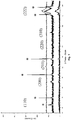
- Fig. 1 includes three X-ray diffraction patterns (Cu k alpha) of crystalline chromium deposited in accordance with an embodiment of the present invention and with hexavalent chromium of the prior art.
- These X-ray diffraction patterns include, at the bottom and the center, a crystalline chromium deposited from trivalent chromium electrolyte T5 with 2 g/L (bottom) and 10 g/L (center) of 3,3'-dithiodipropanoic (DTDP) acid in the trivalent chromium bath, respectively.
- DTDP 3,3'-dithiodipropanoic
- the top sample in contrast, is a conventional chromium deposit from hexavalent electrolyte H4 (as described above).
- the absence of brass substrate peaks (identified by (*) for the center scan; see also Fig. 9 and text relating thereto) indicate thick deposits, greater than -20 microns (the penetration depth of Cu k alpha radiation through chromium).
- the presence of the brass peaks in the 10 g/L DTDP case shows that excess DTDP may diminish cathodic efficiency.
- Fig. 2 is a typical X-ray diffraction pattern (Cu k alpha) of amorphous chromium from a trivalent chromium bath of the prior art. As shown in Fig. 2 , there are no sharp peaks corresponding to regularly occurring positions of atoms in the structure, which would be observed if the chromium deposit were crystalline.
- Fig. 3 is a series of typical X-ray diffraction pattern (Cu k alpha) showing the progressive effect of annealing an amorphous chromium deposit from a trivalent chromium bath of the prior art, containing no sulfur.
- Fig. 3 there is shown a series of X-ray diffraction scans, starting at the lower portion and proceeding upward in Fig. 3 , as the chromium deposit is annealed for longer and longer periods of time.
- the amorphous chromium deposit results in an X-ray diffraction pattern similar to that of Fig.
- the chromium deposit gradually crystallizes, resulting in a pattern of sharp peaks corresponding to the regularly occurring atoms in the ordered crystal structure.
- the lattice parameter of the annealed chromium deposit is in the 2.882 to 2.885 range, although the quality of this series is not good enough to measure accurately.
- Fig. 4 is a series of electron photomicrographs showing the macrocracking effect of annealing an initially amorphous chromium deposit from a trivalent chromium bath of the prior art.
- the chromium layer is the lighter-colored layer deposited on the mottled-appearing substrate.
- macrocracks have formed, while the chromium deposit crystallizes, the macrocracks extend through the thickness of the chromium deposit, down to the substrate.
- the interface between the chromium deposit and the substrate is the faint line running roughly perpendicular to the direction of propagation of the macrocracks, and is marked by the small black square with "P1" within.
- the photomicrograph labeled "1 h at 350°C” after annealing at 350°C for one hour, larger and more definite macrocracks have formed (compared to the "1 h at 250°C” sample), while the chromium deposit crystallizes, the macrocracks extend through the thickness of the chromium deposit, down to the substrate.
- the macrocracks In the photomicrograph labeled "1 h at 450°C", after annealing at 450°C for one hour, the macrocracks have formed and are larger than the lower temperature samples, while the chromium deposit crystallizes, the macrocracks extend through the thickness of the chromium deposit, down to the substrate. In the photomicrograph labeled "1 h at 550°C”, after annealing at 550°C for one hour, the macrocracks have formed and appear to be larger yet than the lower temperature samples, while the chromium deposit crystallizes, the macrocracks extend through the thickness of the chromium deposit, down to the substrate.
- Fig. 5 shows a typical X-ray diffraction pattern (Cu k alpha) of a crystalline as-deposited chromium deposit in accordance with the present invention. As shown in Fig. 5 , the X-ray diffraction peaks are sharp and well defined, showing that the chromium deposit is crystalline, in accordance with the invention.
- Fig. 6 shows typical X-ray diffraction patterns (Cu k alpha) of crystalline chromium deposits in accordance with the present invention.
- the middle two X-ray diffraction patterns shown in Fig. 6 demonstrate strong (222) peaks indicating the ⁇ 111 ⁇ preferred orientation (PO) similar to that observed with crystalline chromium deposited from a hexavalent chromium bath.
- the top and bottom X-ray diffraction patterns shown in Fig. 6 include (200) peaks indicating preferred orientations observed for other crystalline chromium deposits.
- Fig. 7 is a graphical chart illustrating how the concentration of sulfur in one embodiment of a chromium deposit relates to the crystallinity of the chromium deposit.
- the crystallinity axis is assigned a value of one, while if the deposit is amorphous, the crystallinity axis is assigned a value of zero.
- the sulfur content of the chromium deposit ranges from about 1.7 wt.% to about 4 wt.%
- the deposit is crystalline, while outside this range, the deposit is amorphous.
- a crystalline chromium deposit may contain, for example, about 1 wt.% sulfur and be crystalline, and in other embodiments, with this sulfur content, the deposit would be amorphous (as in Fig. 7 ).
- a higher sulfur content for example, up to about 10 wt.%, might be found in a chromium deposit that is crystalline, while in other embodiments, if the sulfur content is greater than 4 wt.%, the deposit may be amorphous.
- sulfur content is important, but not controlling and not the only variable affecting the crystallinity of the trivalent-derived chromium deposit.
- Fig. 8 is a graphical chart comparing the crystal lattice parameter, in Angstroms ( ⁇ ) for a crystalline chromium deposit in accordance with the present invention with crystalline chromium deposits from hexavalent chromium baths and annealed amorphous-as deposited chromium deposits. As shown in Fig.
- the lattice parameter of a crystalline chromium deposit in accordance with the present invention is significantly greater and distinct from the lattice parameter of pyrometallurgically derived chromium ("PyroCr”), is significantly greater and distinct from the lattice parameters of all of the hexavalent chromium deposits ("H1"-"H6"), and is significantly greater and distinct from the lattice parameters of the annealed amorphous-as-deposited chromium deposits ("T1(350°C)", “T1(450°C)" and "T1(550°C)").
- the difference between the lattice parameters of the trivalent crystalline chromium deposits of the present invention and the lattice parameters of the other chromium deposits, such as those illustrated in Fig. 8 , is statistically significant, at least at the 95% confidence level, according to the standard Student's 't' test.
- Fig. 9 is a typical X-ray diffraction pattern (Cu k alpha) showing the progressive effect of increasing amounts of thiosalicylic acid showing the reliably consistent (222) reflection, ⁇ 111 ⁇ preferred orientation, crystalline chromium deposit from a trivalent chromium bath in accordance with an embodiment of the present invention.
- Cu k alpha X-ray diffraction pattern
- crystalline chromium was deposited on brass substrates (peaks from the brass indicated by (*)) from trivalent chromium electrolyte T5 (as described above) electrolyzed at 10 amps per liter (A/L) with nominal 2-6 g/L thiosalicylic acid present to an excess of 140 AH/L demonstrating reliably consistent (222) reflection, ⁇ 111 ⁇ preferred orientation, deposits. The samples were taken at -14 AH intervals.
- the cathodic efficiency ranges from 5% to 80%, and in one embodiment, the cathodic efficiency ranges from 10% to 40%, and in another embodiment, the cathodic efficiency ranges from 10% to 30%.
- additional alloying of the crystalline chromium electrodeposit in which the chromium has a lattice constant of 2.8895 +/- 0.0025 ⁇ , may be performed using ferrous sulfate and sodium hypophosphite as sources of iron and phosphorous with and without the addition of 2 g/L thiosalicylic acid.
- Additions of 0.1g/L to 2 g/L of ferrous ion to electrolyte T7 result in alloys containing 2 to 20% iron.
- the alloys are amorphous without the addition of thiosalicylic acid.
- Additions of 1 to 20 g/L sodium hypophosphite resulted in alloys containing 2 to 12% phosphorous in the deposit. The alloys were amorphous unless thiosalicylic acid is added.
- crystalline chromium deposits having a lattice constant of 2.8895 +/- 0.0025 ⁇ are obtained from electrolyte T7 with 2 g/L thiosalicylic acid agitated using ultrasonic energy at a frequency of 25kHz and 0.5 MHz.
- the resulting deposits are crystalline, having a lattice constant of 2.8895 +/- 0.0025 ⁇ , bright, and there is no significant variation in deposition rate regardless of the frequency used.
Landscapes
- Chemical & Material Sciences (AREA)
- Engineering & Computer Science (AREA)
- Chemical Kinetics & Catalysis (AREA)
- Electrochemistry (AREA)
- Materials Engineering (AREA)
- Metallurgy (AREA)
- Organic Chemistry (AREA)
- Crystallography & Structural Chemistry (AREA)
- Electroplating And Plating Baths Therefor (AREA)
- Electroplating Methods And Accessories (AREA)
Applications Claiming Priority (2)
| Application Number | Priority Date | Filing Date | Title |
|---|---|---|---|
| US78838706P | 2006-03-31 | 2006-03-31 | |
| PCT/US2007/065345 WO2007115030A1 (en) | 2006-03-31 | 2007-03-28 | Crystalline chromium deposit |
Publications (2)
| Publication Number | Publication Date |
|---|---|
| EP2010697A1 EP2010697A1 (en) | 2009-01-07 |
| EP2010697B1 true EP2010697B1 (en) | 2018-03-07 |
Family
ID=38325343
Family Applications (1)
| Application Number | Title | Priority Date | Filing Date |
|---|---|---|---|
| EP07759561.9A Active EP2010697B1 (en) | 2006-03-31 | 2007-03-28 | Crystalline chromium deposit |
Country Status (11)
| Country | Link |
|---|---|
| US (2) | US7887930B2 (es) |
| EP (1) | EP2010697B1 (es) |
| JP (1) | JP5050048B2 (es) |
| KR (1) | KR101367924B1 (es) |
| CN (1) | CN101410556B (es) |
| BR (1) | BRPI0710028B1 (es) |
| CA (1) | CA2647571C (es) |
| ES (1) | ES2669050T3 (es) |
| HK (1) | HK1127099A1 (es) |
| TW (1) | TWI435957B (es) |
| WO (1) | WO2007115030A1 (es) |
Families Citing this family (27)
| Publication number | Priority date | Publication date | Assignee | Title |
|---|---|---|---|---|
| DE102006035871B3 (de) * | 2006-08-01 | 2008-03-27 | Fraunhofer-Gesellschaft zur Förderung der angewandten Forschung e.V. | Verfahren zur Abscheidung von Chromschichten als Hartverchromung, Galvanisierungsbad sowie hartverchromte Oberflächen und deren Verwendung |
| BRPI0817924B1 (pt) * | 2007-10-02 | 2019-02-12 | Atotech Deutschland Gmbh | Depósito de liga de cromo funcional cristalino eletrodepositado, banho de eletrodeposição para eletrodepositar um depósito de liga de cromo funcional cristalinonanogranular, e processo para eletrodepositar um depósito de liga de cromo cristalino funcional nanogranular em um substrato |
| US20090164012A1 (en) * | 2007-12-21 | 2009-06-25 | Howmedica Osteonics Corp. | Medical implant component and method for fabricating same |
| DE102008024271A1 (de) * | 2008-03-01 | 2009-09-10 | Iss Innovative Solarsysteme Gmbh | Verfahren zur Herstellung einer Chromschicht auf einem metallischen Träger |
| DE102008050034B4 (de) * | 2008-10-01 | 2013-02-21 | Voestalpine Stahl Gmbh | Verfahren zum elektrolytischen Abscheiden von Chrom und Chromlegierungen |
| WO2010092622A1 (en) | 2009-02-13 | 2010-08-19 | Nissan Motor Co., Ltd. | Chrome-plated part and manufacturing method of the same |
| US9765437B2 (en) * | 2009-03-24 | 2017-09-19 | Roderick D. Herdman | Chromium alloy coating with enhanced resistance to corrosion in calcium chloride environments |
| FR2962450B1 (fr) * | 2010-07-07 | 2014-10-31 | Commissariat Energie Atomique | Procede de preparation d'un materiau composite, materiau ainsi obtenu et ses utilisations |
| AT510422B1 (de) | 2010-11-04 | 2012-04-15 | Univ Wien Tech | Verfahren zur abscheidung von hartchrom aus cr(vi)- freien elektrolyten |
| PL2705176T3 (pl) | 2011-05-03 | 2016-10-31 | Kąpiel galwaniczna i sposób wytwarzania warstw z ciemnego chromu | |
| US9771661B2 (en) * | 2012-02-06 | 2017-09-26 | Honeywell International Inc. | Methods for producing a high temperature oxidation resistant MCrAlX coating on superalloy substrates |
| US9758884B2 (en) * | 2012-02-16 | 2017-09-12 | Stacey Hingley | Color control of trivalent chromium deposits |
| US20130220819A1 (en) | 2012-02-27 | 2013-08-29 | Faraday Technology, Inc. | Electrodeposition of chromium from trivalent chromium using modulated electric fields |
| EP2899299A1 (en) * | 2014-01-24 | 2015-07-29 | COVENTYA S.p.A. | Electroplating bath containing trivalent chromium and process for depositing chromium |
| US10087540B2 (en) | 2015-02-17 | 2018-10-02 | Honeywell International Inc. | Surface modifiers for ionic liquid aluminum electroplating solutions, processes for electroplating aluminum therefrom, and methods for producing an aluminum coating using the same |
| KR102197508B1 (ko) | 2015-05-12 | 2020-12-31 | 히다치 오토모티브 시스템즈 가부시키가이샤 | 크롬 도금 부품의 제조 방법 및 크롬 도금 장치 |
| JP6295285B2 (ja) | 2016-02-25 | 2018-03-14 | 株式会社豊田中央研究所 | 摺動システム |
| US11149851B2 (en) | 2018-09-13 | 2021-10-19 | Tenneco Inc. | Piston ring with wear resistant coating |
| CN112840065A (zh) * | 2018-10-19 | 2021-05-25 | 德国艾托特克公司 | 用于电解钝化银、银合金、金或金合金表面的方法 |
| CN109371433B (zh) * | 2018-10-31 | 2019-09-20 | 中国人民解放军陆军装甲兵学院 | 一种纳米晶三价铬复合镀层用镀液及复合镀层的制备方法 |
| KR102012739B1 (ko) * | 2018-10-31 | 2019-08-21 | 주식회사 에이엔씨코리아 | 3 가 크롬 도금액 및 이를 이용한 크랙프리 크롬도금공정 |
| WO2020120537A1 (en) * | 2018-12-11 | 2020-06-18 | Atotech Deutschland Gmbh | A method for depositing a chromium or chromium alloy layer and plating apparatus |
| WO2020261930A1 (ja) * | 2019-06-26 | 2020-12-30 | 日立オートモティブシステムズ株式会社 | シリンダ装置と金属製摺動部品及び金属製摺動部品の製造方法 |
| FI129420B (en) | 2020-04-23 | 2022-02-15 | Savroc Ltd | AQUATIC ELECTRIC COATING BATH |
| EP4101947A1 (en) * | 2021-06-10 | 2022-12-14 | Atotech Deutschland GmbH & Co. KG | Method for electrodepositing a dark chromium layer, substrate comprising same, and electroplating bath thereof |
| EP4151779A1 (de) * | 2021-09-15 | 2023-03-22 | Trivalent Oberflächentechnik GmbH | Chrom-indium-, chrom-bismut- und chrom-antimon-beschichtung, verfahren zur herstellung und verwendung |
| WO2024053668A1 (ja) * | 2022-09-07 | 2024-03-14 | 日立Astemo株式会社 | めっき部材およびその製造方法 |
Citations (2)
| Publication number | Priority date | Publication date | Assignee | Title |
|---|---|---|---|---|
| US4062737A (en) * | 1974-12-11 | 1977-12-13 | International Business Machines Corporation | Electrodeposition of chromium |
| JPH03255270A (ja) * | 1990-03-06 | 1991-11-14 | Teikoku Piston Ring Co Ltd | ピストンリング |
Family Cites Families (73)
| Publication number | Priority date | Publication date | Assignee | Title |
|---|---|---|---|---|
| US900597A (en) | 1908-01-16 | 1908-10-06 | Franz Salzer | Process for producing an electrolytic deposit of metallic chromium. |
| US1496845A (en) | 1923-04-13 | 1924-06-10 | Metal & Thermit Corp | Process of producing pure chromium by electrolysis |
| US2470378A (en) | 1944-06-07 | 1949-05-17 | M M Warner | Production of chromium ammonium chloride complexes |
| US2927066A (en) | 1955-12-30 | 1960-03-01 | Glenn R Schaer | Chromium alloy plating |
| US2962428A (en) | 1959-01-15 | 1960-11-29 | Metal & Thermit Corp | Process for chromium plating |
| BE652909A (es) | 1963-12-18 | 1964-12-31 | ||
| FR1563847A (es) | 1968-01-30 | 1969-04-18 | ||
| GB1378883A (en) | 1971-02-23 | 1974-12-27 | Albright & Wilson | Electroplating |
| GB1368749A (en) | 1971-09-30 | 1974-10-02 | British Non Ferrous Metals Res | Electrodeposition of chromium |
| GB1455580A (en) | 1973-12-13 | 1976-11-17 | Albright & Wilson | Electrodeposition of chromium |
| US4054494A (en) | 1973-12-13 | 1977-10-18 | Albright & Wilson Ltd. | Compositions for use in chromium plating |
| US4054740A (en) * | 1974-12-24 | 1977-10-18 | Hoffmann-La Roche Inc. | Hydroxybiotin |
| GB1558169A (en) | 1975-07-03 | 1979-12-19 | Albright & Wilson | Chromium electroplating |
| US4161432A (en) | 1975-12-03 | 1979-07-17 | International Business Machines Corporation | Electroplating chromium and its alloys |
| US4093521A (en) | 1975-12-18 | 1978-06-06 | Stanley Renton | Chromium electroplating |
| DE2606852C2 (de) | 1976-02-20 | 1977-09-15 | Bauer, Wilhelm, Bauer, Hans, Dipl Chem, 3000 Hannover | Bad zur galvanischen Direktverchromung von Kalanderwalzen |
| NL187439C (nl) | 1976-08-06 | 1991-10-01 | Montedison Spa | Werkwijze voor het bereiden van fluorbevattende copolymeren, werkwijze voor het verknopen van copolymeren, membraan voor elektrolyse cel en werkwijze voor de bereiding van gefluoreerde alkenen. |
| JPS53108042A (en) * | 1977-02-28 | 1978-09-20 | Toyo Soda Mfg Co Ltd | Chromium electroplating bath |
| JPS53106348A (en) | 1977-02-28 | 1978-09-16 | Toyo Soda Mfg Co Ltd | Electrolytic bath for chromium plating |
| GB1552263A (en) | 1977-03-04 | 1979-09-12 | Bnf Metals Tech Centre | Trivalent chromium plating baths |
| US4167460A (en) | 1978-04-03 | 1979-09-11 | Oxy Metal Industries Corporation | Trivalent chromium plating bath composition and process |
| GB2051861B (en) | 1979-06-29 | 1983-03-09 | Ibm | Deposition of thick chromium films from trivalent chromium plating solutions |
| US4477318A (en) | 1980-11-10 | 1984-10-16 | Omi International Corporation | Trivalent chromium electrolyte and process employing metal ion reducing agents |
| US4439285A (en) * | 1980-11-10 | 1984-03-27 | Omi International Corporation | Trivalent chromium electrolyte and process employing neodymium reducing agent |
| GB2093861B (en) | 1981-02-09 | 1984-08-22 | Canning Materials W Ltd | Bath for electrodeposition of chromium |
| EP0073221B1 (en) | 1981-03-09 | 1986-01-29 | Battelle Development Corporation | High-rate chromium alloy plating |
| GB2110242B (en) | 1981-11-18 | 1985-06-12 | Ibm | Electroplating chromium |
| GB2109815B (en) | 1981-11-18 | 1985-09-04 | Ibm | Electrodepositing chromium |
| GB2109816B (en) | 1981-11-18 | 1985-01-23 | Ibm | Electrodeposition of chromium |
| GB2109817B (en) | 1981-11-18 | 1985-07-03 | Ibm | Electrodeposition of chromium |
| ATE33686T1 (de) | 1982-02-09 | 1988-05-15 | Ibm | Elektrolytische abscheidung von chrom und seinen legierungen. |
| US4543167A (en) | 1982-03-05 | 1985-09-24 | M&T Chemicals Inc. | Control of anode gas evolution in trivalent chromium plating bath |
| FR2529581A1 (fr) | 1982-06-30 | 1984-01-06 | Armines | Bain d'electrolyse a base de chrome trivalent |
| US4450052A (en) | 1982-07-28 | 1984-05-22 | M&T Chemicals Inc. | Zinc and nickel tolerant trivalent chromium plating baths |
| US4432843A (en) | 1982-07-29 | 1984-02-21 | Omi International Corporation | Trivalent chromium electroplating baths and processes using thiazole addition agents |
| CA1244376A (en) | 1983-05-12 | 1988-11-08 | Thaddeus W. Tomaszewski | Trivalent chromium electrolyte and process |
| US4461680A (en) | 1983-12-30 | 1984-07-24 | The United States Of America As Represented By The Secretary Of Commerce | Process and bath for electroplating nickel-chromium alloys |
| GB8409073D0 (en) | 1984-04-07 | 1984-05-16 | Inter Metals & Minerals Sa | Electrodeposition of chromium &c |
| JPS6156294A (ja) | 1984-08-27 | 1986-03-20 | Nippon Kokan Kk <Nkk> | クロム合金メツキ浴 |
| GB2171114A (en) | 1985-02-06 | 1986-08-20 | Canning W Materials Ltd | Trivalent chromium electroplating baths and rejuvenation thereof |
| US4690735A (en) | 1986-02-04 | 1987-09-01 | University Of Florida | Electrolytic bath compositions and method for electrodeposition of amorphous chromium |
| US4804446A (en) | 1986-09-19 | 1989-02-14 | The United States Of America As Represented By The Secretary Of Commerce | Electrodeposition of chromium from a trivalent electrolyte |
| EP0285931B1 (en) | 1987-03-31 | 1993-08-04 | Nippon Steel Corporation | Corrosion resistant plated steel strip and method for producing same |
| US4960735A (en) * | 1988-11-03 | 1990-10-02 | Kennametal Inc. | Alumina-zirconia-silicon carbide-magnesia ceramics |
| US5770090A (en) | 1989-07-28 | 1998-06-23 | Lewis, Iii; Tom | Method for recovery of heavy metal from waste water |
| JPH03255271A (ja) * | 1990-03-06 | 1991-11-14 | Teikoku Piston Ring Co Ltd | ピストンリング |
| US5269905A (en) | 1990-04-30 | 1993-12-14 | Elf Atochem North America, Inc. | Apparatus and process to regenerate a trivalent chromium bath |
| US5304573A (en) * | 1990-11-17 | 1994-04-19 | Nihon Nohyaku Co., Ltd. | Hydrazone derivatives, processes for production thereof, and uses thereof |
| US5196109A (en) | 1991-08-01 | 1993-03-23 | Geoffrey Scott | Trivalent chromium electrolytes and plating processes employing same |
| US5294326A (en) | 1991-12-30 | 1994-03-15 | Elf Atochem North America, Inc. | Functional plating from solutions containing trivalent chromium ion |
| NO176157C (no) * | 1992-03-24 | 2001-11-21 | Geco As | Fremgangsmåte og innretning til drift av utstyr anbragt i marine, seismiske slep |
| JPH05292300A (ja) | 1992-04-16 | 1993-11-05 | Canon Inc | 画像形成装置 |
| US5433797A (en) | 1992-11-30 | 1995-07-18 | Queen's University | Nanocrystalline metals |
| US5352266A (en) | 1992-11-30 | 1994-10-04 | Queen'university At Kingston | Nanocrystalline metals and process of producing the same |
| US5338433A (en) | 1993-06-17 | 1994-08-16 | Mcdonnell Douglas Corporation | Chromium alloy electrodeposition and surface fixation of calcium phosphate ceramics |
| US5415763A (en) | 1993-08-18 | 1995-05-16 | The United States Of America As Represented By The Secretary Of Commerce | Methods and electrolyte compositions for electrodepositing chromium coatings |
| ZA949293B (en) * | 1993-12-08 | 1995-08-17 | Nihon Nohyaku Co Ltd | Hydrazine derivatives and uses thereof |
| CN1042753C (zh) * | 1994-06-02 | 1999-03-31 | 北京科技大学 | 一种三价铬镀液 |
| FR2726289B1 (fr) | 1994-10-28 | 1997-03-28 | Floquet Monopole | Procede d'electrodeposition d'un revetement de chrome comportant des inclusions solides et bain mis en oeuvre dans ce procede |
| US5578167A (en) | 1996-01-31 | 1996-11-26 | Motorola, Inc. | Substrate holder and method of use |
| US20010054557A1 (en) | 1997-06-09 | 2001-12-27 | E. Jennings Taylor | Electroplating of metals using pulsed reverse current for control of hydrogen evolution |
| JP3918142B2 (ja) | 1998-11-06 | 2007-05-23 | 株式会社日立製作所 | クロムめっき部品、クロムめっき方法およびクロムめっき部品の製造方法 |
| US6911068B2 (en) | 2001-10-02 | 2005-06-28 | Shipley Company, L.L.C. | Plating bath and method for depositing a metal layer on a substrate |
| US6736954B2 (en) | 2001-10-02 | 2004-05-18 | Shipley Company, L.L.C. | Plating bath and method for depositing a metal layer on a substrate |
| US6652731B2 (en) | 2001-10-02 | 2003-11-25 | Shipley Company, L.L.C. | Plating bath and method for depositing a metal layer on a substrate |
| US6773573B2 (en) | 2001-10-02 | 2004-08-10 | Shipley Company, L.L.C. | Plating bath and method for depositing a metal layer on a substrate |
| JP3332374B1 (ja) | 2001-11-30 | 2002-10-07 | ディップソール株式会社 | 亜鉛及び亜鉛合金めっき上に六価クロムフリー防錆皮膜を形成するための処理溶液、六価クロムフリー防錆皮膜及びその形成方法。 |
| JP3332373B1 (ja) | 2001-11-30 | 2002-10-07 | ディップソール株式会社 | 亜鉛及び亜鉛合金めっき上に六価クロムフリー防錆皮膜を形成するための処理溶液、六価クロムフリー防錆皮膜及びその形成方法。 |
| US6979392B2 (en) * | 2002-01-18 | 2005-12-27 | Japan Science And Technology Agency | Method for forming Re—Cr alloy film or Re-based film through electroplating process |
| US7052592B2 (en) | 2004-06-24 | 2006-05-30 | Gueguine Yedigarian | Chromium plating method |
| WO2008057123A1 (en) | 2006-11-09 | 2008-05-15 | Massachusetts Institute Of Technology | Preparation and properties of cr-c-p hard coatings annealed at high temperature for high temperature applications |
| US20080169199A1 (en) | 2007-01-17 | 2008-07-17 | Chang Gung University | Trivalent chromium electroplating solution and an electroplating process with the solution |
| BRPI0817924B1 (pt) | 2007-10-02 | 2019-02-12 | Atotech Deutschland Gmbh | Depósito de liga de cromo funcional cristalino eletrodepositado, banho de eletrodeposição para eletrodepositar um depósito de liga de cromo funcional cristalinonanogranular, e processo para eletrodepositar um depósito de liga de cromo cristalino funcional nanogranular em um substrato |
-
2007
- 2007-03-28 US US11/692,523 patent/US7887930B2/en active Active
- 2007-03-28 CN CN2007800116148A patent/CN101410556B/zh active Active
- 2007-03-28 EP EP07759561.9A patent/EP2010697B1/en active Active
- 2007-03-28 BR BRPI0710028-0A patent/BRPI0710028B1/pt active IP Right Grant
- 2007-03-28 JP JP2009503241A patent/JP5050048B2/ja active Active
- 2007-03-28 KR KR1020087026328A patent/KR101367924B1/ko active IP Right Grant
- 2007-03-28 CA CA2647571A patent/CA2647571C/en active Active
- 2007-03-28 WO PCT/US2007/065345 patent/WO2007115030A1/en active Application Filing
- 2007-03-28 ES ES07759561.9T patent/ES2669050T3/es active Active
- 2007-03-30 TW TW096111396A patent/TWI435957B/zh active
-
2009
- 2009-07-29 HK HK09106989.1A patent/HK1127099A1/xx not_active IP Right Cessation
-
2011
- 2011-02-14 US US13/026,342 patent/US20110132765A1/en not_active Abandoned
Patent Citations (2)
| Publication number | Priority date | Publication date | Assignee | Title |
|---|---|---|---|---|
| US4062737A (en) * | 1974-12-11 | 1977-12-13 | International Business Machines Corporation | Electrodeposition of chromium |
| JPH03255270A (ja) * | 1990-03-06 | 1991-11-14 | Teikoku Piston Ring Co Ltd | ピストンリング |
Also Published As
| Publication number | Publication date |
|---|---|
| US20110132765A1 (en) | 2011-06-09 |
| CA2647571C (en) | 2015-02-17 |
| BRPI0710028B1 (pt) | 2018-02-14 |
| KR101367924B1 (ko) | 2014-03-17 |
| EP2010697A1 (en) | 2009-01-07 |
| JP5050048B2 (ja) | 2012-10-17 |
| KR20090017493A (ko) | 2009-02-18 |
| HK1127099A1 (en) | 2009-09-18 |
| WO2007115030A1 (en) | 2007-10-11 |
| ES2669050T3 (es) | 2018-05-23 |
| TWI435957B (zh) | 2014-05-01 |
| JP2009532580A (ja) | 2009-09-10 |
| US20070227895A1 (en) | 2007-10-04 |
| BRPI0710028A2 (pt) | 2011-08-02 |
| US7887930B2 (en) | 2011-02-15 |
| TW200806816A (en) | 2008-02-01 |
| CN101410556A (zh) | 2009-04-15 |
| CN101410556B (zh) | 2010-12-29 |
| CA2647571A1 (en) | 2007-10-11 |
Similar Documents
| Publication | Publication Date | Title |
|---|---|---|
| EP2010697B1 (en) | Crystalline chromium deposit | |
| EP2217745B1 (en) | Crystalline chromium alloy deposit | |
| EP0925388B1 (en) | Electroplating of nickel-phosphorus alloys coatings | |
| Dolati et al. | The electrodeposition of quaternary Fe–Cr–Ni–Mo alloys from the chloride-complexing agents electrolyte. Part I. Processing | |
| KR101153048B1 (ko) | 철-인 전기 도금 전해조 및 방법 | |
| WO2008057123A1 (en) | Preparation and properties of cr-c-p hard coatings annealed at high temperature for high temperature applications | |
| CN102041529B (zh) | 一种在环保型三价铬镀液中制备镍铬合金复合镀层的方法 | |
| CA1193222A (en) | Electroplating cobalt alloy with zinc or tin from amine bath | |
| Abdel Hamid et al. | Electrodeposition and characterization of chromium–tungsten carbide composite coatings from a trivalent chromium bath | |
| Abd El Rehim et al. | Thin films of chromium electrodeposition from a trivalent chromium electrolyte | |
| US20110281108A1 (en) | Surface cooling | |
| Elias et al. | Development of Ni-P alloy coatings for better corrosion protection using glycerol as additive | |
| VASILACHE | ADVANCED CHARACTERIZATION METHODS FOR NICKEL AND ZINC-NICKEL ALLOY LAYERS ELECTROCHEMICALLY DEPOSITED | |
| Vasilache et al. | STUDIES ABOUT STRUCTURE AND SOME PHYSICAL PROPERTIES OF NICKEL AND ZINC-NICKEL ALLOY LAYERS ELECTROCHEMICALLY DEPOSITED | |
| MXPA06010064A (es) | Metodo y baño galvanoplastico de fosforo y hierro |
Legal Events
| Date | Code | Title | Description |
|---|---|---|---|
| PUAI | Public reference made under article 153(3) epc to a published international application that has entered the european phase |
Free format text: ORIGINAL CODE: 0009012 |
|
| 17P | Request for examination filed |
Effective date: 20081023 |
|
| AK | Designated contracting states |
Kind code of ref document: A1 Designated state(s): AT BE BG CH CY CZ DE DK EE ES FI FR GB GR HU IE IS IT LI LT LU LV MC MT NL PL PT RO SE SI SK TR |
|
| AX | Request for extension of the european patent |
Extension state: AL BA HR MK RS |
|
| RAP1 | Party data changed (applicant data changed or rights of an application transferred) |
Owner name: ATOTECH DEUTSCHLAND GMBH |
|
| DAX | Request for extension of the european patent (deleted) | ||
| 17Q | First examination report despatched |
Effective date: 20140117 |
|
| STAA | Information on the status of an ep patent application or granted ep patent |
Free format text: STATUS: EXAMINATION IS IN PROGRESS |
|
| RIC1 | Information provided on ipc code assigned before grant |
Ipc: C25D 15/00 20060101ALI20170627BHEP Ipc: C25D 3/06 20060101AFI20170627BHEP Ipc: C25D 5/18 20060101ALI20170627BHEP Ipc: C25D 3/10 20060101ALI20170627BHEP |
|
| GRAP | Despatch of communication of intention to grant a patent |
Free format text: ORIGINAL CODE: EPIDOSNIGR1 |
|
| STAA | Information on the status of an ep patent application or granted ep patent |
Free format text: STATUS: GRANT OF PATENT IS INTENDED |
|
| INTG | Intention to grant announced |
Effective date: 20170809 |
|
| GRAJ | Information related to disapproval of communication of intention to grant by the applicant or resumption of examination proceedings by the epo deleted |
Free format text: ORIGINAL CODE: EPIDOSDIGR1 |
|
| STAA | Information on the status of an ep patent application or granted ep patent |
Free format text: STATUS: EXAMINATION IS IN PROGRESS |
|
| INTC | Intention to grant announced (deleted) | ||
| GRAR | Information related to intention to grant a patent recorded |
Free format text: ORIGINAL CODE: EPIDOSNIGR71 |
|
| GRAS | Grant fee paid |
Free format text: ORIGINAL CODE: EPIDOSNIGR3 |
|
| STAA | Information on the status of an ep patent application or granted ep patent |
Free format text: STATUS: GRANT OF PATENT IS INTENDED |
|
| GRAA | (expected) grant |
Free format text: ORIGINAL CODE: 0009210 |
|
| STAA | Information on the status of an ep patent application or granted ep patent |
Free format text: STATUS: THE PATENT HAS BEEN GRANTED |
|
| AK | Designated contracting states |
Kind code of ref document: B1 Designated state(s): AT BE BG CH CY CZ DE DK EE ES FI FR GB GR HU IE IS IT LI LT LU LV MC MT NL PL PT RO SE SI SK TR |
|
| INTG | Intention to grant announced |
Effective date: 20180130 |
|
| REG | Reference to a national code |
Ref country code: GB Ref legal event code: FG4D |
|
| REG | Reference to a national code |
Ref country code: CH Ref legal event code: EP Ref country code: AT Ref legal event code: REF Ref document number: 976660 Country of ref document: AT Kind code of ref document: T Effective date: 20180315 |
|
| REG | Reference to a national code |
Ref country code: FR Ref legal event code: PLFP Year of fee payment: 12 |
|
| REG | Reference to a national code |
Ref country code: IE Ref legal event code: FG4D |
|
| REG | Reference to a national code |
Ref country code: DE Ref legal event code: R096 Ref document number: 602007054152 Country of ref document: DE |
|
| REG | Reference to a national code |
Ref country code: ES Ref legal event code: FG2A Ref document number: 2669050 Country of ref document: ES Kind code of ref document: T3 Effective date: 20180523 |
|
| REG | Reference to a national code |
Ref country code: NL Ref legal event code: MP Effective date: 20180307 |
|
| REG | Reference to a national code |
Ref country code: LT Ref legal event code: MG4D |
|
| PG25 | Lapsed in a contracting state [announced via postgrant information from national office to epo] |
Ref country code: LT Free format text: LAPSE BECAUSE OF FAILURE TO SUBMIT A TRANSLATION OF THE DESCRIPTION OR TO PAY THE FEE WITHIN THE PRESCRIBED TIME-LIMIT Effective date: 20180307 Ref country code: FI Free format text: LAPSE BECAUSE OF FAILURE TO SUBMIT A TRANSLATION OF THE DESCRIPTION OR TO PAY THE FEE WITHIN THE PRESCRIBED TIME-LIMIT Effective date: 20180307 Ref country code: CY Free format text: LAPSE BECAUSE OF FAILURE TO SUBMIT A TRANSLATION OF THE DESCRIPTION OR TO PAY THE FEE WITHIN THE PRESCRIBED TIME-LIMIT Effective date: 20180307 |
|
| REG | Reference to a national code |
Ref country code: AT Ref legal event code: MK05 Ref document number: 976660 Country of ref document: AT Kind code of ref document: T Effective date: 20180307 |
|
| PG25 | Lapsed in a contracting state [announced via postgrant information from national office to epo] |
Ref country code: LV Free format text: LAPSE BECAUSE OF FAILURE TO SUBMIT A TRANSLATION OF THE DESCRIPTION OR TO PAY THE FEE WITHIN THE PRESCRIBED TIME-LIMIT Effective date: 20180307 Ref country code: GR Free format text: LAPSE BECAUSE OF FAILURE TO SUBMIT A TRANSLATION OF THE DESCRIPTION OR TO PAY THE FEE WITHIN THE PRESCRIBED TIME-LIMIT Effective date: 20180608 Ref country code: SE Free format text: LAPSE BECAUSE OF FAILURE TO SUBMIT A TRANSLATION OF THE DESCRIPTION OR TO PAY THE FEE WITHIN THE PRESCRIBED TIME-LIMIT Effective date: 20180307 Ref country code: BG Free format text: LAPSE BECAUSE OF FAILURE TO SUBMIT A TRANSLATION OF THE DESCRIPTION OR TO PAY THE FEE WITHIN THE PRESCRIBED TIME-LIMIT Effective date: 20180607 |
|
| PG25 | Lapsed in a contracting state [announced via postgrant information from national office to epo] |
Ref country code: RO Free format text: LAPSE BECAUSE OF FAILURE TO SUBMIT A TRANSLATION OF THE DESCRIPTION OR TO PAY THE FEE WITHIN THE PRESCRIBED TIME-LIMIT Effective date: 20180307 Ref country code: NL Free format text: LAPSE BECAUSE OF FAILURE TO SUBMIT A TRANSLATION OF THE DESCRIPTION OR TO PAY THE FEE WITHIN THE PRESCRIBED TIME-LIMIT Effective date: 20180307 Ref country code: PL Free format text: LAPSE BECAUSE OF FAILURE TO SUBMIT A TRANSLATION OF THE DESCRIPTION OR TO PAY THE FEE WITHIN THE PRESCRIBED TIME-LIMIT Effective date: 20180307 Ref country code: EE Free format text: LAPSE BECAUSE OF FAILURE TO SUBMIT A TRANSLATION OF THE DESCRIPTION OR TO PAY THE FEE WITHIN THE PRESCRIBED TIME-LIMIT Effective date: 20180307 |
|
| REG | Reference to a national code |
Ref country code: CH Ref legal event code: PL |
|
| PG25 | Lapsed in a contracting state [announced via postgrant information from national office to epo] |
Ref country code: AT Free format text: LAPSE BECAUSE OF FAILURE TO SUBMIT A TRANSLATION OF THE DESCRIPTION OR TO PAY THE FEE WITHIN THE PRESCRIBED TIME-LIMIT Effective date: 20180307 Ref country code: CZ Free format text: LAPSE BECAUSE OF FAILURE TO SUBMIT A TRANSLATION OF THE DESCRIPTION OR TO PAY THE FEE WITHIN THE PRESCRIBED TIME-LIMIT Effective date: 20180307 Ref country code: SK Free format text: LAPSE BECAUSE OF FAILURE TO SUBMIT A TRANSLATION OF THE DESCRIPTION OR TO PAY THE FEE WITHIN THE PRESCRIBED TIME-LIMIT Effective date: 20180307 |
|
| REG | Reference to a national code |
Ref country code: BE Ref legal event code: MM Effective date: 20180331 Ref country code: DE Ref legal event code: R097 Ref document number: 602007054152 Country of ref document: DE |
|
| REG | Reference to a national code |
Ref country code: IE Ref legal event code: MM4A |
|
| PG25 | Lapsed in a contracting state [announced via postgrant information from national office to epo] |
Ref country code: LU Free format text: LAPSE BECAUSE OF NON-PAYMENT OF DUE FEES Effective date: 20180328 Ref country code: PT Free format text: LAPSE BECAUSE OF FAILURE TO SUBMIT A TRANSLATION OF THE DESCRIPTION OR TO PAY THE FEE WITHIN THE PRESCRIBED TIME-LIMIT Effective date: 20180709 |
|
| PLBE | No opposition filed within time limit |
Free format text: ORIGINAL CODE: 0009261 |
|
| STAA | Information on the status of an ep patent application or granted ep patent |
Free format text: STATUS: NO OPPOSITION FILED WITHIN TIME LIMIT |
|
| PG25 | Lapsed in a contracting state [announced via postgrant information from national office to epo] |
Ref country code: IE Free format text: LAPSE BECAUSE OF NON-PAYMENT OF DUE FEES Effective date: 20180328 Ref country code: DK Free format text: LAPSE BECAUSE OF FAILURE TO SUBMIT A TRANSLATION OF THE DESCRIPTION OR TO PAY THE FEE WITHIN THE PRESCRIBED TIME-LIMIT Effective date: 20180307 Ref country code: MC Free format text: LAPSE BECAUSE OF FAILURE TO SUBMIT A TRANSLATION OF THE DESCRIPTION OR TO PAY THE FEE WITHIN THE PRESCRIBED TIME-LIMIT Effective date: 20180307 |
|
| 26N | No opposition filed |
Effective date: 20181210 |
|
| GBPC | Gb: european patent ceased through non-payment of renewal fee |
Effective date: 20180607 |
|
| PG25 | Lapsed in a contracting state [announced via postgrant information from national office to epo] |
Ref country code: LI Free format text: LAPSE BECAUSE OF NON-PAYMENT OF DUE FEES Effective date: 20180331 Ref country code: CH Free format text: LAPSE BECAUSE OF NON-PAYMENT OF DUE FEES Effective date: 20180331 Ref country code: BE Free format text: LAPSE BECAUSE OF NON-PAYMENT OF DUE FEES Effective date: 20180331 Ref country code: SI Free format text: LAPSE BECAUSE OF FAILURE TO SUBMIT A TRANSLATION OF THE DESCRIPTION OR TO PAY THE FEE WITHIN THE PRESCRIBED TIME-LIMIT Effective date: 20180307 |
|
| PG25 | Lapsed in a contracting state [announced via postgrant information from national office to epo] |
Ref country code: GB Free format text: LAPSE BECAUSE OF NON-PAYMENT OF DUE FEES Effective date: 20180607 |
|
| PG25 | Lapsed in a contracting state [announced via postgrant information from national office to epo] |
Ref country code: MT Free format text: LAPSE BECAUSE OF NON-PAYMENT OF DUE FEES Effective date: 20180328 |
|
| PG25 | Lapsed in a contracting state [announced via postgrant information from national office to epo] |
Ref country code: TR Free format text: LAPSE BECAUSE OF FAILURE TO SUBMIT A TRANSLATION OF THE DESCRIPTION OR TO PAY THE FEE WITHIN THE PRESCRIBED TIME-LIMIT Effective date: 20180307 |
|
| PG25 | Lapsed in a contracting state [announced via postgrant information from national office to epo] |
Ref country code: HU Free format text: LAPSE BECAUSE OF FAILURE TO SUBMIT A TRANSLATION OF THE DESCRIPTION OR TO PAY THE FEE WITHIN THE PRESCRIBED TIME-LIMIT; INVALID AB INITIO Effective date: 20070328 |
|
| PG25 | Lapsed in a contracting state [announced via postgrant information from national office to epo] |
Ref country code: IS Free format text: LAPSE BECAUSE OF FAILURE TO SUBMIT A TRANSLATION OF THE DESCRIPTION OR TO PAY THE FEE WITHIN THE PRESCRIBED TIME-LIMIT Effective date: 20180707 |
|
| PGFP | Annual fee paid to national office [announced via postgrant information from national office to epo] |
Ref country code: FR Payment date: 20230322 Year of fee payment: 17 |
|
| PGFP | Annual fee paid to national office [announced via postgrant information from national office to epo] |
Ref country code: IT Payment date: 20230328 Year of fee payment: 17 Ref country code: ES Payment date: 20230527 Year of fee payment: 17 |
|
| PGFP | Annual fee paid to national office [announced via postgrant information from national office to epo] |
Ref country code: DE Payment date: 20240320 Year of fee payment: 18 |