EP2009969A2 - Systeme und Verfahren zur Härtung einer abgelagerten Schicht auf einem Substrat - Google Patents
Systeme und Verfahren zur Härtung einer abgelagerten Schicht auf einem Substrat Download PDFInfo
- Publication number
- EP2009969A2 EP2009969A2 EP08252094A EP08252094A EP2009969A2 EP 2009969 A2 EP2009969 A2 EP 2009969A2 EP 08252094 A EP08252094 A EP 08252094A EP 08252094 A EP08252094 A EP 08252094A EP 2009969 A2 EP2009969 A2 EP 2009969A2
- Authority
- EP
- European Patent Office
- Prior art keywords
- curing
- light
- laser
- deposited layer
- substrate
- Prior art date
- Legal status (The legal status is an assumption and is not a legal conclusion. Google has not performed a legal analysis and makes no representation as to the accuracy of the status listed.)
- Withdrawn
Links
Images


Classifications
-
- B—PERFORMING OPERATIONS; TRANSPORTING
- B23—MACHINE TOOLS; METAL-WORKING NOT OTHERWISE PROVIDED FOR
- B23K—SOLDERING OR UNSOLDERING; WELDING; CLADDING OR PLATING BY SOLDERING OR WELDING; CUTTING BY APPLYING HEAT LOCALLY, e.g. FLAME CUTTING; WORKING BY LASER BEAM
- B23K26/00—Working by laser beam, e.g. welding, cutting or boring
- B23K26/02—Positioning or observing the workpiece, e.g. with respect to the point of impact; Aligning, aiming or focusing the laser beam
- B23K26/06—Shaping the laser beam, e.g. by masks or multi-focusing
- B23K26/062—Shaping the laser beam, e.g. by masks or multi-focusing by direct control of the laser beam
- B23K26/0622—Shaping the laser beam, e.g. by masks or multi-focusing by direct control of the laser beam by shaping pulses
-
- C—CHEMISTRY; METALLURGY
- C21—METALLURGY OF IRON
- C21D—MODIFYING THE PHYSICAL STRUCTURE OF FERROUS METALS; GENERAL DEVICES FOR HEAT TREATMENT OF FERROUS OR NON-FERROUS METALS OR ALLOYS; MAKING METAL MALLEABLE, e.g. BY DECARBURISATION OR TEMPERING
- C21D1/00—General methods or devices for heat treatment, e.g. annealing, hardening, quenching or tempering
- C21D1/06—Surface hardening
-
- B—PERFORMING OPERATIONS; TRANSPORTING
- B05—SPRAYING OR ATOMISING IN GENERAL; APPLYING FLUENT MATERIALS TO SURFACES, IN GENERAL
- B05D—PROCESSES FOR APPLYING FLUENT MATERIALS TO SURFACES, IN GENERAL
- B05D3/00—Pretreatment of surfaces to which liquids or other fluent materials are to be applied; After-treatment of applied coatings, e.g. intermediate treating of an applied coating preparatory to subsequent applications of liquids or other fluent materials
- B05D3/06—Pretreatment of surfaces to which liquids or other fluent materials are to be applied; After-treatment of applied coatings, e.g. intermediate treating of an applied coating preparatory to subsequent applications of liquids or other fluent materials by exposure to radiation
-
- B—PERFORMING OPERATIONS; TRANSPORTING
- B23—MACHINE TOOLS; METAL-WORKING NOT OTHERWISE PROVIDED FOR
- B23K—SOLDERING OR UNSOLDERING; WELDING; CLADDING OR PLATING BY SOLDERING OR WELDING; CUTTING BY APPLYING HEAT LOCALLY, e.g. FLAME CUTTING; WORKING BY LASER BEAM
- B23K26/00—Working by laser beam, e.g. welding, cutting or boring
- B23K26/02—Positioning or observing the workpiece, e.g. with respect to the point of impact; Aligning, aiming or focusing the laser beam
- B23K26/03—Observing, e.g. monitoring, the workpiece
-
- B—PERFORMING OPERATIONS; TRANSPORTING
- B23—MACHINE TOOLS; METAL-WORKING NOT OTHERWISE PROVIDED FOR
- B23K—SOLDERING OR UNSOLDERING; WELDING; CLADDING OR PLATING BY SOLDERING OR WELDING; CUTTING BY APPLYING HEAT LOCALLY, e.g. FLAME CUTTING; WORKING BY LASER BEAM
- B23K26/00—Working by laser beam, e.g. welding, cutting or boring
- B23K26/08—Devices involving relative movement between laser beam and workpiece
- B23K26/082—Scanning systems, i.e. devices involving movement of the laser beam relative to the laser head
-
- H—ELECTRICITY
- H05—ELECTRIC TECHNIQUES NOT OTHERWISE PROVIDED FOR
- H05K—PRINTED CIRCUITS; CASINGS OR CONSTRUCTIONAL DETAILS OF ELECTRIC APPARATUS; MANUFACTURE OF ASSEMBLAGES OF ELECTRICAL COMPONENTS
- H05K3/00—Apparatus or processes for manufacturing printed circuits
- H05K3/10—Apparatus or processes for manufacturing printed circuits in which conductive material is applied to the insulating support in such a manner as to form the desired conductive pattern
- H05K3/12—Apparatus or processes for manufacturing printed circuits in which conductive material is applied to the insulating support in such a manner as to form the desired conductive pattern using thick film techniques, e.g. printing techniques to apply the conductive material or similar techniques for applying conductive paste or ink patterns
- H05K3/1283—After-treatment of the printed patterns, e.g. sintering or curing methods
-
- H—ELECTRICITY
- H05—ELECTRIC TECHNIQUES NOT OTHERWISE PROVIDED FOR
- H05K—PRINTED CIRCUITS; CASINGS OR CONSTRUCTIONAL DETAILS OF ELECTRIC APPARATUS; MANUFACTURE OF ASSEMBLAGES OF ELECTRICAL COMPONENTS
- H05K3/00—Apparatus or processes for manufacturing printed circuits
- H05K3/22—Secondary treatment of printed circuits
-
- H—ELECTRICITY
- H10—SEMICONDUCTOR DEVICES; ELECTRIC SOLID-STATE DEVICES NOT OTHERWISE PROVIDED FOR
- H10P—GENERIC PROCESSES OR APPARATUS FOR THE MANUFACTURE OR TREATMENT OF DEVICES COVERED BY CLASS H10
- H10P95/00—Generic processes or apparatus for manufacture or treatments not covered by the other groups of this subclass
- H10P95/90—Thermal treatments, e.g. annealing or sintering
-
- B—PERFORMING OPERATIONS; TRANSPORTING
- B23—MACHINE TOOLS; METAL-WORKING NOT OTHERWISE PROVIDED FOR
- B23K—SOLDERING OR UNSOLDERING; WELDING; CLADDING OR PLATING BY SOLDERING OR WELDING; CUTTING BY APPLYING HEAT LOCALLY, e.g. FLAME CUTTING; WORKING BY LASER BEAM
- B23K2101/00—Articles made by soldering, welding or cutting
- B23K2101/36—Electric or electronic devices
- B23K2101/40—Semiconductor devices
-
- H—ELECTRICITY
- H05—ELECTRIC TECHNIQUES NOT OTHERWISE PROVIDED FOR
- H05K—PRINTED CIRCUITS; CASINGS OR CONSTRUCTIONAL DETAILS OF ELECTRIC APPARATUS; MANUFACTURE OF ASSEMBLAGES OF ELECTRICAL COMPONENTS
- H05K1/00—Printed circuits
- H05K1/02—Details
- H05K1/09—Use of materials for the conductive, e.g. metallic pattern
- H05K1/092—Dispersed materials, e.g. conductive pastes or inks
- H05K1/095—Dispersed materials, e.g. conductive pastes or inks for polymer thick films, i.e. having a permanent organic polymeric binder
-
- H—ELECTRICITY
- H05—ELECTRIC TECHNIQUES NOT OTHERWISE PROVIDED FOR
- H05K—PRINTED CIRCUITS; CASINGS OR CONSTRUCTIONAL DETAILS OF ELECTRIC APPARATUS; MANUFACTURE OF ASSEMBLAGES OF ELECTRICAL COMPONENTS
- H05K2203/00—Indexing scheme relating to apparatus or processes for manufacturing printed circuits covered by H05K3/00
- H05K2203/10—Using electric, magnetic and electromagnetic fields; Using laser light
- H05K2203/107—Using laser light
-
- H—ELECTRICITY
- H05—ELECTRIC TECHNIQUES NOT OTHERWISE PROVIDED FOR
- H05K—PRINTED CIRCUITS; CASINGS OR CONSTRUCTIONAL DETAILS OF ELECTRIC APPARATUS; MANUFACTURE OF ASSEMBLAGES OF ELECTRICAL COMPONENTS
- H05K3/00—Apparatus or processes for manufacturing printed circuits
- H05K3/0008—Apparatus or processes for manufacturing printed circuits for aligning or positioning of tools relative to the circuit board
-
- H—ELECTRICITY
- H10—SEMICONDUCTOR DEVICES; ELECTRIC SOLID-STATE DEVICES NOT OTHERWISE PROVIDED FOR
- H10K—ORGANIC ELECTRIC SOLID-STATE DEVICES
- H10K71/00—Manufacture or treatment specially adapted for the organic devices covered by this subclass
- H10K71/40—Thermal treatment, e.g. annealing in the presence of a solvent vapour
- H10K71/421—Thermal treatment, e.g. annealing in the presence of a solvent vapour using coherent electromagnetic radiation, e.g. laser annealing
Definitions
- the present invention is directed to systems and methods for curing layers deposited on a substrate, including printed layers of a printed electronics.
- micro-electric components that may be produced include capacitors, resistors, diodes, and transistors, while examples of complete devices may include RFID tags, sensors, flexible displays, etc.
- a capacitor can be constructed by depositing a conducting layer, followed by depositing an insulating layer and then another conducting layer. To obtain higher capacitance, either this process can be repeated or different material or material thicknesses may be utilized.
- a transistor can be formed by depositing a conductor layer forming source and drain electrodes, a semiconductor layer, a dielectric layer, and another conductor layer forming a gate electrode.
- Printed electronics forming complete functional devices may be produced at a very low cost when low-cost conducting and semiconducting materials, such as organic polymers, are used, and are believe to be somewhat less expensive to fabricate than analogous integrated circuits. Such low-cost printed electronics are not expected to compete directly with silicon-based integrated circuits. Rather, printed electronics may be produced to offer, for example, lower performance (e.g., lower frequency, lower power, or shorter lifetime) at much lower cost as compared to silicon-based integrated circuits.
- lower performance e.g., lower frequency, lower power, or shorter lifetime
- Printed electronics are typically made using a set of materials, including dielectrics, conductors, and semi-conductors, that are deposited in a wet printing process. These are usually printable solutions, suspensions, or emulsions containing polymers, polymer precursors, inorganic materials, and organic or inorganic additives. Typical wet printing methods that may be employed include letterpress printing, screen printing, and ink jet printing. Specifically, these printable materials are deposited in a desired sequence onto a substrate. Once the layers are deposited onto the substrate, the printed electronics is often cured using a large convection oven.
- a curing system comprising a support having a planar surface for supporting a substrate having a material deposited thereon, a curing device comprising a laser capable of emitting a beam of light onto at least a portion of the deposited layer of material, and a control system connected in electrical communication with the curing device.
- a method of curing at least one deposited layer in a process of fabricating a printed electronics comprising a plurality of layers deposited onto a substrate includes emitting a beam of light from a laser and illuminating a deposited layer with the emitted beam of light, and moving the beam of light onto selected portions of the deposited layer.
- a method of fabricating a printed electronics includes(a) supporting a substrate with a support having a planar surface, (b) depositing via a printing device one of more materials onto the substrate in selected patterns, thereby forming a plurality of printed layers, and (c) laser curing at least a portion of each printed layer.
- the curing methods and systems according to embodiments of the present invention when used for printed electronics fabrication, may provide many benefits and advantages, including but not limited to, simplifying printed electronics fabrication, increasing throughput, reducing equipment cost and size, lowering curing energy requirements, and possibly decreasing volatile organic compounds given off in the curing process. This latter factor may allow smaller hoods, fans, and related solvent handling hardware needed to process these vapors and improved safety for operating personnel.
- FIGURE 1 there is shown a schematic diagram depicting one exemplary curing system, generally designated 20, which is formed in accordance with aspects of the present invention.
- the system 20 includes a planar support surface 22 for supporting a substrate 24 having at least one layer 26 deposited thereon, at least one curing device 28 for curing the at least one deposited layer 26, and a control system 32 for controlling the overall curing process.
- the support surface 22 is defined by the top of a stationary or movable bed or platen 36.
- the substrate 24 may be placed on the bed or platen 34 manually or by automated material handling equipment (not shown) such as in-feeders, pick and place material handlers, etc.
- the support surface 22 may be a portion of a substrate advancement apparatus (not shown), such as a conveyor belt, conveyor tracks, or the like.
- the substrate 24 may be also in web form, and advanced with respect to the curing system 20 via substrate advancement apparatuses known in the art.
- the support surface 22 may be defined by a bed or platen positioned under the curing device, which supports the web of substrate.
- the curing device 28 is a device that cures one or more layers of material that has been deposited onto a substrate.
- the deposited material is printed for fabricating printed electronics
- curing allows for the printed material to attain desirable electronic or electrical properties.
- the curing device 28 cures the layers of material by means of local heating, solvent evaporation, chemical reactions, etc. It will be appreciate that the deposited material may include a catalyst to initiate or accelerate the chemical reaction(s).
- the curing device 28 includes at least one laser 40, a lens module 42, and an optional modulator 44.
- the laser 40 is capable of generating a concentrated beam of laser light 46 that illuminates at least a portion of the deposited layer 26.
- Any laser type may be suitable for use in embodiments of the present invention.
- semiconductor lasers, gas lasers (helium-neon, argon, or carbon dioxide), excimer lasers, etc. may be used. It will be appreciated that the type of laser chosen may depend, in part, on the type of materials deposited so that the laser has sufficient power to achieve the desired level of curing.
- the laser 40 can be turned on and off by means of electrical signal from the control system 32.
- the lens module 42 of the curing system 28 is disposed below the laser 40.
- the lens module 42 is capable of adjusting the focus of the light 46 emitted from the laser 40, which can be controlled with electrical signals from the control system 32.
- Focus adjustability provides the ability to dynamically maintain a desired laser beam illumination area on the deposited layer 26, for example, a printed electronics layer, on substrate 24. It may also be desirable in several embodiments where sufficient laser power is available, to defocus the beam of laser light using lens module 42 to create a larger illumination area. Thus a larger area could be cured at one time. This can make it possible to achieve a shorter overall curing time.
- By means of dynamic control of the illumination area high-resolution could be achieved where desired by refocusing the lens module 42 to make a small illumination area when desired.
- the curing device 28 may optionally include a modulator 44 positioned below the lens module 42.
- the beam of laser light 46 exiting the lens module 42 passes through the modulator 44, which is configured to vary the intensity of the beam of laser light passing therethrough. Such modulation can be done by one of several methods well known in the art.
- the amount of light passed by the modulator 44 can be controlled with electrical signals from the control system 32.
- the curing device 28 is mounted on a conventional X-Y table 50.
- the movement of the laser 40, and thus the placement of the beam of laser light 46 can be advantageously controlled in an XY plane parallel to the planar support surface 22 in order to cure the layer of material at desired locations.
- the curing device 28 is mounted for movement on an X-Y table 50 in the embodiments heretofore described, it should be appreciated that other configurations may also be utilized.
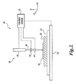
- the bed or platen 36 that defines the support surface 22 can be mounted on an X-Y table 54, and moved with respect to the curing device 28, as best shown in the embodiment of FIGURE 2 .
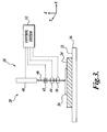
- an X-Y beam deflecting module 56 may be utilized instead.
- the laser 40, lens module 42, and optional modulator 44 are fixed in a stationary position.
- the X-Y beam deflecting module 56 controls the angle of the beam in both the X and Y directions so as to illuminate the deposited layer of material at a selected position.
- a hybrid system may be utilized for providing suitable operational performance.
- the hybrid system could include a beam deflecting module that deflects the laser light in one direction, e.g., the X direction, and a movement table supporting the substrate for motion in another direction, e.g., the Y direction.
- a beam deflecting module that deflects the laser light in one direction, e.g., the X direction
- a movement table supporting the substrate for motion in another direction e.g., the Y direction.
- a movement table supporting the substrate for motion in another direction e.g., the Y direction.
- the Y direction e.g., the Y direction
- both an X-Y beam deflecting module 56 and an X-Y motion table 50 and/or 54 could be used. This system provides both high speed and high precision positioning of the beam of laser light along both X and Y axes.
- the X-Y motion table 54 could move the support surface 22 and substrate 24 under a stationary laser 40,
- the system 20 further includes a control system 32, which controls at least the curing process.
- the control system 32 may comprise a computer or other processor appropriately programmed for controlling the curing process.
- the control system 32 includes a computer with stored programs, data, etc., and various input/output circuitry to transmit the proper control signals to control the operation of the laser 40, the lens module 42, the optional modulator 44, the beam deflecting module 56, X-Y tables 50 and 54, a substrate advancement apparatus, material handling equipment, etc.
- a substrate such as substrate 24 having a deposited layer 26 thereon, is supported by the support surface 22 in a suitable position with respect to the curing device 28.
- the substrate 24 may be placed onto the support surface 22 manually or transferred thereto by one of any number of automated material handling systems.
- the curing device 28 is suitably operated to cure the deposited layer of material.
- the control system 32 sends appropriate control signals to turn on the laser 40, focus the lens module 42, modulate the intensity of the beam of laser light via the modulator 44 if desired, and direct the focused beam of laser light 46 onto a selected portion of the deposited layer of material.
- the focused beam of laser light 46 may be directed by one of the following methods: 1) controlling the position of the X-Y beam deflecting module 56 to direct the focused beam of laser light 46 onto a desired illumination area of the deposited layer of material; 2) controlling the position of the laser 40 via the X-Y table 50, or 3) controlling the position of the substrate 22 via the X-Y table 54.
- the beam of laser light 46 is then appropriately moved, for example, in a raster scan, to apply photons to specific portions of the deposited layer of material. This curing process continues until as much of the deposited layer has been cured as desired.
- the dose of photons from the beam of laser light 46 is controlled. This can be accomplished either by turning the laser 40 off and on as the beam is positioned over each desired portion of the deposited material, or by controlling the intensity (e.g., by using a modulator 44) and/or the speed of movement of the laser light as it moves along a path of the area being cured.
- suitable curing may be achievable using non-constant laser intensity at each position of the deposited layer of material. For example, improved curing may be attained by using a short high-intensity pulse of laser light followed by a longer lower intensity pulse, or visa-versa.
- Embodiments of the present invention having the capability of controlling the dose of photons of the beam of laser light may also provide improved curing of the deposited layers when it is desired, for example, that certain areas of the deposited layer to have a larger dose than others. For example, edges of traces and areas over a region of high thermal conductivity may require a larger dose of photons to cure these portions of the deposited layers more completely. Controlling the photon dose to provide the minimum dose necessary at each position on the deposited layer also provides a shorter cure time for each layer compared with a uniform dose large enough to cure the most-difficult-to-cure region of the deposited material.
- An additional advantage may be realized with the capability of controlling the dose of photons in that such a system can accommodate individual curing characteristics and requirements for each material from the set of materials. This is particularly desirable when fabricating printed electronics.
- a layer of material in an area greater than necessary and curing only a selected portion thereof. This may enable lower-cost, lower precision, and faster completion times. Curing only part of the deposited layer of material can be done by curing only a small area at a time with a focused beam of laser light and then moving the beam of laser light with respect to the substrate 24 in conjunction with turning the laser off and on or variable control of beam intensity so that all desired areas of the deposited material are cured.
- the beam of laser light of a single laser may be split into multiple beams if sufficient laser power is available. This can be done for example by a two-dimensional diffraction pattern. By these means, curing of more than one spot on the polymer could be done simultaneously.
- a light sensor or image sensor 60 may be included in the system 20.
- the light sensor or image sensor 60 is capable of viewing the deposited layer of material as it is being cured.
- the output of this sensor (or these sensors) is monitored by the control system 32 and used to control the curing process.
- Suitable sensors might be CCD or CMOS video sensors, or visible light or infrared photo-sensors. By this means ; improved curing performance, quality, and/or speed may be achieved.
- the image sensor could also be used to view the fiducial marks on the printed electronics to assist in registration of the laser beam position.
- the sensor(s) could also detect and read identification and/or serial numbers on the printed electronics, and with this information the control system 32 can choose the desired curing pattern and algorithm for curing the current particular electronics type and deposited material from the data stored in its memory.
- the curing system 20 may be part of a printed electronics fabrication system 120.
- the printed electronics fabrication system 120 includes at least one printing device 110 for depositing one or more layers of material in selected patterns onto the substrate 24 for forming a printed electronics, such s a capacitor, transistor, etc., and the curing system 20 for curing one or more layers of deposited material.
- the control system 32 may also control the printing process or the system 120 may include a separate print control system (not shown).
- the system 120 may include separate printing and curing stations such that the substrate is transferred and properly aligned between the printing and curing stations via any known material handling system, such as a conveyor assembly, a pick and place system using a robot arm, etc, or the substrate could be in web form and transferred in any manner known in the art.
- any known material handling system such as a conveyor assembly, a pick and place system using a robot arm, etc, or the substrate could be in web form and transferred in any manner known in the art.
- the layers of the printed electronics are deposited and cured sequentially in an additive process.
Landscapes
- Engineering & Computer Science (AREA)
- Physics & Mathematics (AREA)
- Optics & Photonics (AREA)
- Plasma & Fusion (AREA)
- Mechanical Engineering (AREA)
- Manufacturing & Machinery (AREA)
- Microelectronics & Electronic Packaging (AREA)
- Chemical & Material Sciences (AREA)
- Materials Engineering (AREA)
- Crystallography & Structural Chemistry (AREA)
- Thermal Sciences (AREA)
- Metallurgy (AREA)
- Organic Chemistry (AREA)
- Formation Of Insulating Films (AREA)
- Semiconductor Lasers (AREA)
- Manufacturing Of Printed Wiring (AREA)
- Laser Beam Processing (AREA)
- Heating, Cooling, Or Curing Plastics Or The Like In General (AREA)
- Liquid Deposition Of Substances Of Which Semiconductor Devices Are Composed (AREA)
- Drying Of Semiconductors (AREA)
Applications Claiming Priority (1)
| Application Number | Priority Date | Filing Date | Title |
|---|---|---|---|
| US11/771,722 US20090004368A1 (en) | 2007-06-29 | 2007-06-29 | Systems and methods for curing a deposited layer on a substrate |
Publications (2)
| Publication Number | Publication Date |
|---|---|
| EP2009969A2 true EP2009969A2 (de) | 2008-12-31 |
| EP2009969A3 EP2009969A3 (de) | 2010-11-17 |
Family
ID=39916529
Family Applications (1)
| Application Number | Title | Priority Date | Filing Date |
|---|---|---|---|
| EP08252094A Withdrawn EP2009969A3 (de) | 2007-06-29 | 2008-06-18 | Systeme und Verfahren zur Härtung einer abgelagerten Schicht auf einem Substrat |
Country Status (6)
| Country | Link |
|---|---|
| US (1) | US20090004368A1 (de) |
| EP (1) | EP2009969A3 (de) |
| JP (2) | JP2009076859A (de) |
| KR (1) | KR20090004483A (de) |
| CN (1) | CN101337219A (de) |
| SG (1) | SG148958A1 (de) |
Families Citing this family (4)
| Publication number | Priority date | Publication date | Assignee | Title |
|---|---|---|---|---|
| KR101083320B1 (ko) * | 2011-03-11 | 2011-11-14 | 한국기계연구원 | 경화 시스템 및 그 방법 |
| JP5869669B2 (ja) | 2011-07-01 | 2016-02-24 | ヒューレット−パッカード デベロップメント カンパニー エル.ピー.Hewlett‐Packard Development Company, L.P. | 硬化装置、画像形成装置、及び、製造品 |
| KR102850075B1 (ko) * | 2014-04-30 | 2025-08-25 | 카티바, 인크. | 가스 쿠션 장비 및 기판 코팅 기술 |
| CN109507768A (zh) * | 2018-11-29 | 2019-03-22 | 交通运输部公路科学研究所 | 微尺度光学结构加工装置 |
Family Cites Families (46)
| Publication number | Priority date | Publication date | Assignee | Title |
|---|---|---|---|---|
| DE2735231A1 (de) * | 1977-08-04 | 1979-02-15 | Siemens Ag | Verfahren und vorrichtung zur herstellung von loetverbindungen mittels energiestrahlung |
| JPH0795538B2 (ja) * | 1986-05-02 | 1995-10-11 | 旭硝子株式会社 | レ−ザ−アニ−ル装置 |
| JPH0730362B2 (ja) * | 1987-03-20 | 1995-04-05 | 株式会社日立製作所 | 電子部品及びその製造方法 |
| US5302954A (en) * | 1987-12-04 | 1994-04-12 | Magellan Corporation (Australia) Pty. Ltd. | Identification apparatus and methods |
| DE3741916C2 (de) * | 1987-12-10 | 1996-07-18 | Resma Gmbh Fuegetechnik Indust | Verfahren zum Aushärten von Klebstoffen auf Kunststoffbasis |
| US5656229A (en) * | 1990-02-20 | 1997-08-12 | Nikon Corporation | Method for removing a thin film layer |
| US5204823A (en) * | 1991-03-20 | 1993-04-20 | Calcomp Inc. | Method and apparatus for high-speed layer thickness curing in 3-D model making |
| US5300756A (en) * | 1991-10-22 | 1994-04-05 | General Scanning, Inc. | Method for severing integrated-circuit connection paths by a phase-plate-adjusted laser beam |
| JPH05133375A (ja) * | 1991-11-14 | 1993-05-28 | Matsushita Electric Ind Co Ltd | 電動圧縮機 |
| US5264061A (en) * | 1992-10-22 | 1993-11-23 | Motorola, Inc. | Method of forming a three-dimensional printed circuit assembly |
| JPH0766536A (ja) * | 1993-08-30 | 1995-03-10 | Fujitsu Ten Ltd | 配線の印刷方法及び該方法に使用する印刷装置 |
| GB9520888D0 (en) * | 1995-10-12 | 1995-12-13 | Philips Electronics Nv | Electronic devices comprising thin-film circuitry |
| DE69729816T2 (de) * | 1996-01-31 | 2005-07-21 | Texas Instruments Deutschland Gmbh | Verbesserung für Vollweggleichrichter |
| JP4346684B2 (ja) * | 1996-04-17 | 2009-10-21 | コーニンクレッカ フィリップス エレクトロニクス エヌ ヴィ | 基板上への焼結体の製造方法 |
| JP3085451B2 (ja) * | 1996-04-22 | 2000-09-11 | 富士通株式会社 | 製造ラインおよびそれによって製造される多層プリント配線基板 |
| JPH1098251A (ja) * | 1996-09-23 | 1998-04-14 | Matsushita Electric Ind Co Ltd | 蒸着された金属配線および誘電配線のuvレーザーアニーリングおよび洗浄 |
| DE69830846T2 (de) * | 1997-09-11 | 2006-05-24 | Precision Dynamics Corp., San Fernando | Radiofrequenzidentifikationsetikett auf flexiblem substrat |
| US6121130A (en) * | 1998-11-16 | 2000-09-19 | Chartered Semiconductor Manufacturing Ltd. | Laser curing of spin-on dielectric thin films |
| US6203952B1 (en) * | 1999-01-14 | 2001-03-20 | 3M Innovative Properties Company | Imaged article on polymeric substrate |
| US6524346B1 (en) * | 1999-02-26 | 2003-02-25 | Micron Technology, Inc. | Stereolithographic method for applying materials to electronic component substrates and resulting structures |
| US6151446A (en) * | 1999-07-06 | 2000-11-21 | Applied Materials, Inc. | Apparatus and method for thermally processing substrates including a processor using multiple detection signals |
| US6134130A (en) * | 1999-07-19 | 2000-10-17 | Motorola, Inc. | Power reception circuits for a device receiving an AC power signal |
| WO2001051243A2 (en) * | 2000-01-10 | 2001-07-19 | Electro Scientific Industries, Inc. | Laser system and method for processing a memory link with a burst of laser pulses having ultrashort pulsewidths |
| JP2001332658A (ja) * | 2000-03-14 | 2001-11-30 | Hitachi Ltd | 半導体集積回路装置およびその製造方法 |
| US6718128B2 (en) * | 2000-06-28 | 2004-04-06 | Fisher & Paykel Healthcare Limited | Radiant warmer with distance determination between heater and patient |
| DE10044842A1 (de) * | 2000-09-11 | 2002-04-04 | Siemens Ag | Organischer Gleichrichter, Schaltung, RFID-Tag und Verwendung eines organischen Gleichrichters |
| US6414543B1 (en) * | 2000-11-28 | 2002-07-02 | Precision Dynamics Corporation | Rectifying charge storage element |
| JP4822588B2 (ja) * | 2001-02-08 | 2011-11-24 | 富士通セミコンダクター株式会社 | 情報処理装置および情報処理デバイス |
| US6639177B2 (en) * | 2001-03-29 | 2003-10-28 | Gsi Lumonics Corporation | Method and system for processing one or more microstructures of a multi-material device |
| DE10212640B4 (de) * | 2002-03-21 | 2004-02-05 | Siemens Ag | Logische Bauteile aus organischen Feldeffekttransistoren |
| JP4532058B2 (ja) * | 2002-08-26 | 2010-08-25 | 日本発條株式会社 | 修正方法、修正装置及び修正プログラム |
| US7161590B2 (en) * | 2002-09-04 | 2007-01-09 | John James Daniels | Thin, lightweight, flexible, bright, wireless display |
| JP2004223789A (ja) * | 2003-01-21 | 2004-08-12 | Seiko Instruments Inc | 観察機能付きマイクロ光造形装置 |
| US7682970B2 (en) * | 2003-07-16 | 2010-03-23 | The Regents Of The University Of California | Maskless nanofabrication of electronic components |
| US7026581B2 (en) * | 2003-08-22 | 2006-04-11 | Axcelis Technologies, Inc. | Apparatus for positioning an elevator tube |
| US7494923B2 (en) * | 2004-06-14 | 2009-02-24 | Semiconductor Energy Laboratory Co., Ltd. | Manufacturing method of wiring substrate and semiconductor device |
| US7245371B2 (en) * | 2004-08-27 | 2007-07-17 | B & W Tek, Inc. | Laser curing apparatus with real-time monitoring and control |
| DE102004059467A1 (de) * | 2004-12-10 | 2006-07-20 | Polyic Gmbh & Co. Kg | Gatter aus organischen Feldeffekttransistoren |
| JP2006310346A (ja) * | 2005-04-26 | 2006-11-09 | Seiko Epson Corp | 機能性膜パターン形成装置、機能性膜パターンの形成方法及び電子機器 |
| DE602006004913D1 (de) * | 2005-04-28 | 2009-03-12 | Semiconductor Energy Lab | Verfahren und Vorrichtung zur Herstellung von Halbleitern mittels Laserstrahlung |
| JP2006332568A (ja) * | 2005-05-30 | 2006-12-07 | Daiken Kagaku Kogyo Kk | 導電パターン生成方法 |
| JP2007039716A (ja) * | 2005-08-01 | 2007-02-15 | Shin Caterpillar Mitsubishi Ltd | レーザー光によるメッキ層剥離方法、加工メッキ鋼板、作業機械の防錆燃料タンク及びレーザー加工機 |
| GB2432714A (en) * | 2005-10-06 | 2007-05-30 | Seiko Epson Corp | Thin film transistor and method for fabricating an electronic device |
| US7622378B2 (en) * | 2005-11-09 | 2009-11-24 | Tokyo Electron Limited | Multi-step system and method for curing a dielectric film |
| US8956457B2 (en) * | 2006-09-08 | 2015-02-17 | Tokyo Electron Limited | Thermal processing system for curing dielectric films |
| US7599048B2 (en) * | 2007-02-09 | 2009-10-06 | Wafermasters, Inc. | Optical emission spectroscopy process monitoring and material characterization |
-
2007
- 2007-06-29 US US11/771,722 patent/US20090004368A1/en not_active Abandoned
-
2008
- 2008-05-29 KR KR1020080049966A patent/KR20090004483A/ko not_active Ceased
- 2008-06-18 EP EP08252094A patent/EP2009969A3/de not_active Withdrawn
- 2008-06-18 SG SG200804612-0A patent/SG148958A1/en unknown
- 2008-06-24 JP JP2008164040A patent/JP2009076859A/ja active Pending
- 2008-06-30 CN CNA2008101295461A patent/CN101337219A/zh active Pending
-
2012
- 2012-02-13 JP JP2012028826A patent/JP2012182448A/ja active Pending
Also Published As
| Publication number | Publication date |
|---|---|
| KR20090004483A (ko) | 2009-01-12 |
| EP2009969A3 (de) | 2010-11-17 |
| CN101337219A (zh) | 2009-01-07 |
| JP2012182448A (ja) | 2012-09-20 |
| US20090004368A1 (en) | 2009-01-01 |
| SG148958A1 (en) | 2009-01-29 |
| JP2009076859A (ja) | 2009-04-09 |
Similar Documents
| Publication | Publication Date | Title |
|---|---|---|
| US8463116B2 (en) | Systems for curing deposited material using feedback control | |
| JP5539646B2 (ja) | デバイスのパターニング | |
| US8916796B2 (en) | Method for depositing and curing nanoparticle-based ink | |
| KR101813548B1 (ko) | 레이저 열전사 장치 및 이를 이용한 유기 발광 표시 장치의 제조 방법 | |
| EP1599340B1 (de) | Ultravioletthärtung | |
| EP2009969A2 (de) | Systeme und Verfahren zur Härtung einer abgelagerten Schicht auf einem Substrat | |
| CN1387997A (zh) | 用于生成一个印刷块的方法和设备 | |
| CN112599462A (zh) | 移转设备及移转方法 | |
| JP2013527809A (ja) | 印刷装置及び印刷装置を制御する方法 | |
| US11464116B2 (en) | Lithographic exposure system and method for exposure and curing a solder resist | |
| US20170197279A1 (en) | Apparatus and methods for performing laser ablation on a substrate | |
| US20220050380A1 (en) | Apparatus and method for exposing printing plates using light emitting diodes | |
| TW200828643A (en) | Manufacturing equipment of display device and manufacturing method of display device | |
| KR20090042711A (ko) | 직접 상 노광장치 | |
| KR101000003B1 (ko) | 액정 표시 장치의 회로 결함 보수 방법 및 장치 | |
| US11158841B2 (en) | Method for manufacturing organic el display device | |
| WO2013133196A1 (ja) | パターン形成方法及びパターン形成基板の製造方法 | |
| CN100508141C (zh) | 薄膜晶体管的形成方法 | |
| US20030217996A1 (en) | Method for simultaneous laser beam soldering | |
| US20140065294A1 (en) | Surface conditioning for depositing and curing nanoparticle-based ink | |
| US20140147791A1 (en) | Processing apparatus for processing a flexographic plate, a method and a computer program product | |
| KR20140142856A (ko) | 레이저 장치 및 이를 이용한 결정화 방법 | |
| KR100979780B1 (ko) | 디바이스의 패터닝 | |
| EP1640107B1 (de) | Verfahren zur Herstellung einer organischen elektrolumineszierenden Anzeigevorrichtung | |
| JP2020101821A (ja) | パターン形成装置 |
Legal Events
| Date | Code | Title | Description |
|---|---|---|---|
| PUAI | Public reference made under article 153(3) epc to a published international application that has entered the european phase |
Free format text: ORIGINAL CODE: 0009012 |
|
| AK | Designated contracting states |
Kind code of ref document: A2 Designated state(s): AT BE BG CH CY CZ DE DK EE ES FI FR GB GR HR HU IE IS IT LI LT LU LV MC MT NL NO PL PT RO SE SI SK TR |
|
| AX | Request for extension of the european patent |
Extension state: AL BA MK RS |
|
| PUAL | Search report despatched |
Free format text: ORIGINAL CODE: 0009013 |
|
| AK | Designated contracting states |
Kind code of ref document: A3 Designated state(s): AT BE BG CH CY CZ DE DK EE ES FI FR GB GR HR HU IE IS IT LI LT LU LV MC MT NL NO PL PT RO SE SI SK TR |
|
| AX | Request for extension of the european patent |
Extension state: AL BA MK RS |
|
| RIC1 | Information provided on ipc code assigned before grant |
Ipc: B23K 26/08 20060101ALI20101008BHEP Ipc: H05K 3/12 20060101AFI20081111BHEP |
|
| REG | Reference to a national code |
Ref country code: DE Ref legal event code: R108 |
|
| AKY | No designation fees paid | ||
| REG | Reference to a national code |
Ref country code: DE Ref legal event code: R108 Effective date: 20110714 |
|
| STAA | Information on the status of an ep patent application or granted ep patent |
Free format text: STATUS: THE APPLICATION IS DEEMED TO BE WITHDRAWN |
|
| 18D | Application deemed to be withdrawn |
Effective date: 20110415 |