EP2006349B1 - Strahlendetektorelement und davon gebrauch machender strahlendetektor - Google Patents
Strahlendetektorelement und davon gebrauch machender strahlendetektor Download PDFInfo
- Publication number
- EP2006349B1 EP2006349B1 EP07715019.1A EP07715019A EP2006349B1 EP 2006349 B1 EP2006349 B1 EP 2006349B1 EP 07715019 A EP07715019 A EP 07715019A EP 2006349 B1 EP2006349 B1 EP 2006349B1
- Authority
- EP
- European Patent Office
- Prior art keywords
- diamond film
- film
- light emission
- beam detector
- polycrystalline diamond
- Prior art date
- Legal status (The legal status is an assumption and is not a legal conclusion. Google has not performed a legal analysis and makes no representation as to the accuracy of the status listed.)
- Not-in-force
Links
Images


Classifications
-
- G—PHYSICS
- G01—MEASURING; TESTING
- G01T—MEASUREMENT OF NUCLEAR OR X-RADIATION
- G01T1/00—Measuring X-radiation, gamma radiation, corpuscular radiation, or cosmic radiation
- G01T1/29—Measurement performed on radiation beams, e.g. position or section of the beam; Measurement of spatial distribution of radiation
-
- C—CHEMISTRY; METALLURGY
- C23—COATING METALLIC MATERIAL; COATING MATERIAL WITH METALLIC MATERIAL; CHEMICAL SURFACE TREATMENT; DIFFUSION TREATMENT OF METALLIC MATERIAL; COATING BY VACUUM EVAPORATION, BY SPUTTERING, BY ION IMPLANTATION OR BY CHEMICAL VAPOUR DEPOSITION, IN GENERAL; INHIBITING CORROSION OF METALLIC MATERIAL OR INCRUSTATION IN GENERAL
- C23C—COATING METALLIC MATERIAL; COATING MATERIAL WITH METALLIC MATERIAL; SURFACE TREATMENT OF METALLIC MATERIAL BY DIFFUSION INTO THE SURFACE, BY CHEMICAL CONVERSION OR SUBSTITUTION; COATING BY VACUUM EVAPORATION, BY SPUTTERING, BY ION IMPLANTATION OR BY CHEMICAL VAPOUR DEPOSITION, IN GENERAL
- C23C16/00—Chemical coating by decomposition of gaseous compounds, without leaving reaction products of surface material in the coating, i.e. chemical vapour deposition [CVD] processes
- C23C16/02—Pretreatment of the material to be coated
- C23C16/0254—Physical treatment to alter the texture of the surface, e.g. scratching or polishing
-
- C—CHEMISTRY; METALLURGY
- C23—COATING METALLIC MATERIAL; COATING MATERIAL WITH METALLIC MATERIAL; CHEMICAL SURFACE TREATMENT; DIFFUSION TREATMENT OF METALLIC MATERIAL; COATING BY VACUUM EVAPORATION, BY SPUTTERING, BY ION IMPLANTATION OR BY CHEMICAL VAPOUR DEPOSITION, IN GENERAL; INHIBITING CORROSION OF METALLIC MATERIAL OR INCRUSTATION IN GENERAL
- C23C—COATING METALLIC MATERIAL; COATING MATERIAL WITH METALLIC MATERIAL; SURFACE TREATMENT OF METALLIC MATERIAL BY DIFFUSION INTO THE SURFACE, BY CHEMICAL CONVERSION OR SUBSTITUTION; COATING BY VACUUM EVAPORATION, BY SPUTTERING, BY ION IMPLANTATION OR BY CHEMICAL VAPOUR DEPOSITION, IN GENERAL
- C23C16/00—Chemical coating by decomposition of gaseous compounds, without leaving reaction products of surface material in the coating, i.e. chemical vapour deposition [CVD] processes
- C23C16/22—Chemical coating by decomposition of gaseous compounds, without leaving reaction products of surface material in the coating, i.e. chemical vapour deposition [CVD] processes characterised by the deposition of inorganic material, other than metallic material
- C23C16/26—Deposition of carbon only
- C23C16/27—Diamond only
- C23C16/274—Diamond only using microwave discharges
-
- C—CHEMISTRY; METALLURGY
- C23—COATING METALLIC MATERIAL; COATING MATERIAL WITH METALLIC MATERIAL; CHEMICAL SURFACE TREATMENT; DIFFUSION TREATMENT OF METALLIC MATERIAL; COATING BY VACUUM EVAPORATION, BY SPUTTERING, BY ION IMPLANTATION OR BY CHEMICAL VAPOUR DEPOSITION, IN GENERAL; INHIBITING CORROSION OF METALLIC MATERIAL OR INCRUSTATION IN GENERAL
- C23C—COATING METALLIC MATERIAL; COATING MATERIAL WITH METALLIC MATERIAL; SURFACE TREATMENT OF METALLIC MATERIAL BY DIFFUSION INTO THE SURFACE, BY CHEMICAL CONVERSION OR SUBSTITUTION; COATING BY VACUUM EVAPORATION, BY SPUTTERING, BY ION IMPLANTATION OR BY CHEMICAL VAPOUR DEPOSITION, IN GENERAL
- C23C16/00—Chemical coating by decomposition of gaseous compounds, without leaving reaction products of surface material in the coating, i.e. chemical vapour deposition [CVD] processes
- C23C16/22—Chemical coating by decomposition of gaseous compounds, without leaving reaction products of surface material in the coating, i.e. chemical vapour deposition [CVD] processes characterised by the deposition of inorganic material, other than metallic material
- C23C16/26—Deposition of carbon only
- C23C16/27—Diamond only
- C23C16/277—Diamond only using other elements in the gas phase besides carbon and hydrogen; using other elements besides carbon, hydrogen and oxygen in case of use of combustion torches; using other elements besides carbon, hydrogen and inert gas in case of use of plasma jets
Definitions
- the present invention relates to a beam detector for detecting the position, intensity, and the like of beam light by irradiating a beam irradiation portion with the beams, such as high-energy synchrotron radiation, generated by a synchrotron radiation facility or the like and to a beam monitor using the above beam detector.
- a beam detector for detecting the position, intensity, and the like of beam light by irradiating a beam irradiation portion with the beams, such as high-energy synchrotron radiation, generated by a synchrotron radiation facility or the like and to a beam monitor using the above beam detector.
- Fig. 8 is a schematic structural view showing one example of an x-ray beam monitor device according to a conventional example
- Fig. 9 includes an overhead view and a cross-sectional view, each schematically illustrating one example of a synchrotron radiation position.monitor according to a conventional example
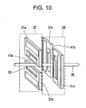
- Fig. 10 is a perspective view showing the structure of one example of a beam monitor according to a conventional example.
- the transmission x-ray beam monitor device has the structure in which photoelectric films 14 and 15 are formed on a half of a front surface and a half of a rear surface of a monitor plate 12.
- this x-ray beam monitor when x-ray beams 11 are irradiated, electrons (photoelectrons) are emitted from the photoelectric films 14 and 15, and the electron amounts emitted from the individual surfaces are measured by secondary electron multiplier tubes 16a and 16b. Since the photoelectric film 14 on the front surface and the photoelectric film 15 on the rear surface are disposed so as not to be overlapped with each other, one-dimensional displacement of the beams 11 from the central position can be measured (see Patent Document 1).
- the above x-ray beam monitor according to the conventional example can estimate the one-dimensional central position (for example, along the x coordinate) but cannot determine a two-dimensional position (along the y coordinate).
- a second beam monitor is necessarily provided so as to be perpendicular to the first beam monitor.
- the synchrotron radiation position monitor according to the conventional example uses a vapor phase-synthesized diamond plate 21 in the form of a disc having a bore 22 at the center, and around the periphery thereof, four divided metal electrodes 23 and 23' in the form of fans are disposed on two surfaces of the diamond plate 21.
- the metal electrodes 23 and 23' are irradiated with synchrotron radiation, since photoelectrons are emitted, by monitoring a photoelectron current, the central position of the radiation beams is estimated.
- the synchrotron radiation position monitor according to the conventional example since the four divided metal electrodes 23 and 23' are disposed, the (x, y) coordinates of the central position of the radiation beams can be determined (see Patent Document 2).
- the beam central position is estimated from current of photoelectrons generated from the electrodes 23 and 23' facing each other with the diamond plate 21 interposed therebetween.
- the estimation as described above can be reasonable as long as the cross-sectional distribution of beam intensity has a perfect circular shape.
- the cross-sectional distribution of beam intensity may show a deformed oval shape or a shape including two circles overlapped with each other, and in addition, the cross-sectional distribution changes with time.
- the synchrotron radiation position monitor according to the conventional example has problems in that the beam position cannot be precisely estimated and in that the change in cross-sectional distribution cannot also be grasped. Furthermore, by the monitoring method according to the conventional example, when radiation beams are largely shifted from the bore 22 located at the center of the synchrotron radiation position monitor, it does not work at all. That is, there has been a self-contradiction that when the position of the radiation beams is not known beforehand, the radiation beam position cannot be monitored.
- a synchrotron radiation position monitor since a synchrotron radiation position monitor according to another conventional example has a structure similar to that shown in Fig. 9 , it will be described with reference to Fig. 9 ; that is, the method of this monitor is that current (photocurrent) between the electrodes 23 and 23' disposed on the two surfaces of the diamond plate 21 is measured instead of that caused by electron emission, so that the central position of radiation beams is estimated.
- the synchrotron radiation position monitor of the above conventional example is a monitor to measure photocurrent flowing between the electrodes 23 and 23' facing each other with the diamond plate 21 interposed therebetween, as shown in Fig. 9 .
- the film quality of a diamond plate formed by a vapor phase synthesis is not uniform, even when beams are irradiated to a position monitor in a symmetrical manner, outputs from individual electrodes cannot be equivalent to each other, and as a result, there has been a problem in that the beam position cannot be precisely estimated.
- Patent Document 2 when the radiation beams are largely shifted from the center of the synchrotron radiation position monitor, it does not work at all.
- a beam monitor proposed as another conventional example has a first unit 37 composed of a pair of diamond plates 31a and 31b, which are disposed so that the end surfaces thereof are separated parallel to each other and which each have electrodes 33 on two surfaces, and a second unit 38 disposed apart from the first unit 37 in the direction in which beams to be measured travel.
- At least one set of a pair of diamond plates 31c and 31d which are disposed so that the end surfaces thereof are separated parallel to each other and which each have electrodes 33 on two surfaces, is disposed in the direction in which beams 36 to be measured travel, and at least one set of diamond plates among the diamond plates 31a, 31b, 31c, and 31d forming the first unit 37 and the second unit 38 can adjust gaps 41a and 41b therebetween (see Patent Document 4).
- EP0736780 discloses an x-ray beam position monitor, including a diamond plate placed so that the X-ray beam pass through the diamond plate, and a plurality of electrode pairs placed on both sides of the diamond plate.
- a low resistivity to be formed in the diamond plate can be formed by doping sufficient amount of impurities while diamond is made grown by vapor phase synthesis.
- Impurities to be doped include, for instance, B, Al, Li, P and Se.
- the above beam monitor is formed by doping boron in the diamond plates 31a, 31b, 31c, and 31d.
- the measurement principle of the beam monitor according to this conventional example is to measure current generated in the diamond plates, and in order to obtain a diamond plate having a low resistivity, the doping is merely performed using boron.
- the synchrotron radiation position monitor proposed in the Patent Document 2 according to the above conventional example there has been a problem similar to that of the synchrotron radiation position monitor proposed in the Patent Document 2 according to the above conventional example.
- the present invention has been conceived in consideration of the problems described above, and an object of the present invention is to provide a beam detector and a beam monitor using the same, the beam detector being capable of precisely and stably detecting, for a long period of time, the position, the intensity distribution, and the change with time of radiation beams, soft x-ray beams, and the like, which are from high energy to low energy; and being manufactured at a low cost as compared to that of a conventional detection device.
- At least one beam irradiation portion of the beam detector for detecting the position and intensity of beams is formed of a free-standing diamond film, and this diamond film is a polycrystalline diamond film (C) containing at least one element (X) selected from the group consisting of silicon (Si), nitrogen (N), lithium (Li), beryllium (Be), boron (B), phosphorus (P), sulfur (S), nickel (Ni), and vanadium (V).
- element (X) selected from the group consisting of silicon (Si), nitrogen (N), lithium (Li), beryllium (Be), boron (B), phosphorus (P), sulfur (S), nickel (Ni), and vanadium (V).
- the beam detector is characterized in that since the beam detector is designed so that at least one element selected from the above elements X is contained in the polycrystalline diamond film at an X/C of 0.1 to 1,000 ppm, a light emission function of emitting light is imparted to the polycrystalline diamond film when it is irradiated with beams.
- the beam detector is also characterized in that the beams are synchrotron radiation beams and the diamond film uses a polycrystalline diamond film which emits light in a beam irradiation region at an energy of 5 to 300 keV.
- the beam detector is also characterized in that at least part of the diamond film is held by a substrate and the polycrystalline diamond film has a film thickness of 0.1 ⁇ m to 3 mm.
- the beam detector is also characterized in that the polycrystalline diamond film includes diamond grains having an average grain diameter of 0.1 ⁇ m to 1 mm.
- the beam detector is also characterized in that the light emission wavelength is 150 to 800 nm.
- the beam detector is also characterized in that the light emission has a peak intensity in a wavelength region of 730 to 760 nm.
- the beam detector is also characterized in that the light emission has a peak intensity in a wavelength region of 500 to 600 nm.
- the beam detector is also characterized in that the polycrystalline diamond film has a surface flatness of 30 to 100 nm.
- the beam detector is also characterized in that a plurality of the beam detectors is assembled to form a module structure.
- the beam detector is also characterized in that the polycrystalline diamond film forms a free-standing film structure and this free-standing film portion is the beam irradiation portion to be irradiated with beams.
- the beam detector is also characterized in that the polycrystalline diamond film includes the beam irradiation portion and a thick film portion having a thickness larger than that of the beam irradiation portion.
- the beam detector is also characterized in that the substrate is a silicon substrate or a composite in which a thin film of silicon dioxide is provided between a substrate and a polycrystalline diamond film.
- Means employed by a beam monitor according to the present invention is characterized in that a beam monitor having a beam detector for detecting the position and intensity of beams, comprises the beam detector of the present invention and light emission observation means for observing the above light emission phenomenon, and in that by a light emission state observed by this light emission observation means, the position and intensity of the beams are detected.
- the beam monitor is also characterized in that the beams are radiation beams, the diamond film uses a polycrystalline diamond film which emits light in a beam irradiation region at an energy of 5 to 300 keV, and the light emission observation means includes a camera.
- the beam detector of the present invention includes a beam irradiation portion, which is formed using at least a polycrystalline diamond film, for detecting the position and intensity of beams, and this polycrystalline diamond film is a polycrystalline diamond (C) film containing at least one element (X) selected from the group consisting of silicon (Si), nitrogen (N), lithium (Li), beryllium (Be), boron (B), phosphorus (P), sulfur (S), nickel (Ni), and vanadium (V) at an X/C of 0.1 to 1,000 ppm, when the beams are irradiated to this diamond film, a light emission function of emitting light is imparted thereto: hence, monochromatic light, such as visible light or ultraviolet light, having sufficient intensity can be obtained from a beam irradiation spot.
- X element
- the diamond film uses a polycrystalline diamond film which emits light in a beam radiation region at an energy of 5 to 300 keV, and the light emission wavelength is 150 to 800 nm, when light emission is in the visible light region, the irradiation spot of the radiation beams can be recognized by the naked eye, and hence the irradiation position of the beams can be identified by the naked eye.
- the film thickness of the polycrystalline diamond film is 0.1 ⁇ m to 3 mm, and the average grain diameter of diamond grains is 0.1 ⁇ m to 1 mm, high-quality transmission radiation beams having a suitable light emission region size and appropriate light emission luminance can be obtained.
- the light emission has a peak intensity in a wavelength region of 730 to 760 nm or 500 to 600 nm, which is the light emission relating to silicon (Si) and boron (B), respectively, contained in the polycrystalline diamond film, the light emission intensity is particularly significant; hence, the light emission can be easily detected, so that the beam position can be identified.
- the surface flatness of the polycrystalline diamond film is 30 to 100 nm, the light emission intensity by radiation beams is improved by 2 to 5 times as compared to that of an unpolished diamond film.
- the beam detector of the present invention since a plurality of beam detectors is assembled to form a module structure, the positions and intensities of plural types of irradiation beams can be simultaneously detected and observed.
- the polycrystalline diamond film forms a free-standing film structure, and since this free-standing film portion is the beam irradiation portion to be irradiated with beams, no breakage occurs even by large current electron beams.
- the polycrystalline diamond film includes the beam irradiation portion and a thick film portion having a thickness larger than that of the beam irradiation portion, an increase in temperature of the beam irradiation portion can be suppressed.
- the substrate is a silicon substrate or a composite in which a thin film of silicon dioxide is provided between a substrate and a polycrystalline diamond film, the flatness of the substrate and the perpendicularity thereof to radiation beams can be easily ensured.
- the beam monitor of the present invention which is a beam monitor having a beam detector for detecting the position and intensity of beams, since the beam detector and light emission observation means for observing the above light emission phenomenon are provided, even when the light emission is performed in an invisible light region, by a light emission state observed by this light emission observation means, the position and intensity of the beams can be detected.
- the diamond film uses a polycrystalline diamond film which emits light in a beam irradiation region at an energy of 5 to 300 keV
- the light emission observation means includes a camera
- radiation beams in a wide wavelength region and in a wide energy range, which correspond to from a soft x-ray region to an ultraviolet ray region can be monitored, and in addition, a clear spot image can be taken by using the above camera.
- a video camera or the like as the camera, the position and the intensity distribution of radiation beams can be measured in real time.
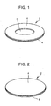
- Fig. 1 is a schematic perspective view schematically showing a front surface of the beam detector according to the embodiment 1 of the present invention
- Fig. 2 is a schematic perspective view schematically showing a rear surface of the beam detector according to the embodiment 1 of the present invention
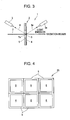
- Fig. 3 is a schematic cross-sectional view schematically showing an entire structure of a beam monitor using the beam detector according to the embodiment 1 of the present invention.
- a polycrystalline diamond (C) film 4 is formed on a rear surface of a substrate 5, and the substrate 5 is a frame having a ring shape which is formed only along the periphery of the diamond film.
- the polycrystalline diamond film 4 is doped, for example, with silicon (Si) at an atomic ratio Si/C of 0.1 to 1,000 ppm.
- the atomic ratio Si/C is less than 0.1 ppm, the light emission intensity is excessively low, and when the Si/C is more than 1,000 ppm, the crystallinity of the diamond film 4 is degraded, so that the light emission intensity is decreased.
- the atomic ratio Si/C is preferably in a range of 1 to 100 ppm and more preferably in a range of 5 to 50 ppm.
- element (X) selected from the group consisting of silicon (Si), nitrogen (N), lithium (Li), beryllium (Be), boron (B), phosphorus (P), sulfur (S), nickel (Ni), and vanadium (V).
- the element X as mentioned above is doped at an atomic ratio X/C of 0.1 to 1,000 ppm, and the polycrystalline diamond film 4 is irradiated with beams, from the radiation beam irradiation spot 7a, visible light, ultraviolet light, or the like having sufficient intensity can be obtained.
- the upper and the lower limits and the desired range of the total concentration (X/C) of the above impurities are similar to those in the case of the above Si.
- the substrate in a region of the beam irradiation portion 6 through which the radiation beams 7 are allowed to pass when being irradiated is removed, and the polycrystalline diamond film 4 has a free-standing structure as shown in Fig. 3 .
- the structure as described above can be formed, for example, by the steps of using silicon as the substrate 5, masking a region other than that to be removed using an acid-resistant material, and then performing etching with a hydrofluoric acid-nitric acid solution.
- the film thickness of the polycrystalline diamond film 4 be set small, such as 5 to 30 ⁇ m, at the beam irradiation portion 6 and be set large, such as 70 to 100 ⁇ m, at the other part on the substrate 5.
- the film thickness distribution of the polycrystalline diamond film 4 as described above can be realized using a selective growth technique of the diamond film 4. As described above, the reason the thickness of the diamond film 4 is set small at the beam irradiation portion 6 and is set large at the other part is to suppress an increase in temperature of the beam irradiation portion 6.
- the beam detector 2 of the present invention has a simple structure as shown in Figs. 1 and 2 , compared to the beam detectors each requiring a complicated production process disclosed in the Patent Documents 1 to 4 according to the conventional examples, the manufacturing cost can be significantly reduced.
- a synchrotron radiation detector 1 according to the embodiment 1 of the present invention has the beam detector 2 according to the embodiment 1 of the present invention as described above, and a light emission observation means 3 disposed at the irradiation side of the radiation beams 7.
- the polycrystalline diamond film 4 forming the beam irradiation portion 6 of the above beam detector 2 is irradiated with the radiation beams 7 to perform the light emission 8 from the polycrystalline diamond film 4, and this light emission 8 is observed by the light emission observation means 3, so that the irradiation spot 7a and the intensity of the beam light 7 are detected.
- the above light emission observation means 3 can use a general optical camera or digital camera, an ultraviolet CCD camera, a video camera, or the like.
- the film thickness of the polycrystalline diamond film 4 the optimum value thereof is determined by the energy or energy density of the incident radiation beams 7.
- an appropriate film thickness of the polycrystalline diamond film 4 is 0.1 ⁇ m to 3 mm.
- the film thickness is less than 0.1 ⁇ m, since the light emission region is excessively small, the intensity of light emission is very low.
- the film thickness of the polycrystalline diamond film 4 is more preferably in a range of 3 to 20 ⁇ m.
- the grain diameter of the polycrystalline diamond film 4 has the relationship with the light emission luminance, and the average grain diameter is preferably in a range of 0.1 ⁇ m to 1 mm.
- the average grain diameter is less than 0.1 ⁇ m, the amount of a non-diamond component is increased in the polycrystalline diamond film 4, and the crystalline defect density is also increased thereby, so that the light emission luminance is degraded.
- the average grain diameter of diamond is more preferably in a range of 1 to 10 ⁇ m.
- the light emission 8 having a light emission wavelength in a range of 150 to 800 nm can be emitted from the polycrystalline diamond film 4.
- the irradiation spot 7a of the radiation beams 7 can be recognized by the naked eye, and when the light emission 8 is in a region having a wavelength shorter than the visible light, by using an ultraviolet CCD camera as the light emission observation means 3, the irradiation spot 7a can be identified.
- the surface flatness of the polycrystalline diamond film 4 is preferably in a range of 30 to 100 nm.
- the surface flatness of the polycrystalline diamond film 4 is set in a range of 30 to 100 nm, the light emission intensity by the radiation beams 7 is improved by 2 to 5 times.
- the reasons the surface flatness is set as described above are that when the surface flatness is set to less than 30 nm, since a process must be performed for a particularly long time for forming the polycrystalline diamond, and polish-planarization of the film surface must be performed for a particularly long time, the cost is excessively increased, and that on the other hand, when the surface flatness is more than 100 nm, a light extraction rate is degraded by scattering of light at the film surface.
- the surface flatness of the polycrystalline diamond film 4 can be improved by performing a mechanical and/or a chemical mechanical polishing process on the surface of this diamond film 4.
- a chemical mechanical polishing method in which diamond is immersed in a polishing liquid containing abrasive grains, such as alumina, silica, or titania, dispersed in water, and polishing is performed on the surface of the diamond by abrasion, or a method in which in a vacuum chamber capable of controlling an oxygen partial pressure and an internal temperature, diamond is polished while metal oxides of iron, nickel, cobalt, and copper are reduced by carbon present in a surface layer portion of the diamond.
- the surface flatness can be easily measured by a stylus step measuring meter or a microscope using interference/phase difference of laser light.
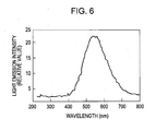
- Fig. 4 is a schematic plan view schematically showing a front surface of the beam detector according to the embodiment 2 of the present invention.
- the difference of the embodiment 2 from the embodiment 1 of the present invention is that an entire structure of the beam detector is not formed as that shown in Fig. 1 .
- the same constituent elements as those of the embodiment 1 are designated by the same reference numerals as described above, and the different point will be describe below.
- a plurality of beam irradiation portions 6 is connected to each other in a plane to form a module structure.
- a detection range of beams can be increased.
- connection may be performed to form a curved surface.
- Fig. 5 is an observation example of a light emission spectrum from the beam monitor according to the present invention, which has a beam detector including a polycrystalline diamond film doped with silicon (Si)
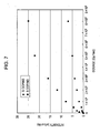
- Fig. 6 is an observation example of a light emission spectrum from the beam monitor according to the present invention, which has a beam detector including a polycrystalline diamond film doped with boron (B).
- the light emission preferably has a peak intensity in a wavelength region of 730 to 760 nm or 500 to 600 nm.
- the reason for this is that when the light emission 8 is in a wavelength range of 730 to 760 nm or 500 to 600 nm, which relates to silicon (Si) or boron (B), respectively, contained in the polycrystalline diamond film, since the intensity thereof is particularly significant, the light emission can be easily detected, and hence the beam position can be identified.
- the beam detector 2 of the present invention is formed using diamond having a high thermal conductivity, no local overheating occurs at the radiation beam spot 7a.
- diamond is formed of carbon, which has a small atomic number (that is, small number of electrons)
- the beam detector is characterized in that the interaction with radiation rays 7 is small and the absorption thereof hardly occurs. Accordingly, by providing the beam detectors 2 at the incident side and the transmission side of the radiation beams 7 with respect to a sample the position and the change in intensity of the radiation beams 7 can also be measured.
- the surface flatness and the degree of parallelization (perpendicularity to the radiation beams) of the polycrystalline diamond film 4 of a free-standing diamond film 6 may become important in some cases.
- the grown surface of the polycrystalline diamond film 4 may be planarized by polishing or a silicon wafer having a flat surface may be used as the substrate, so that the surface flatness can be ensured.
- the beam detector 2 of the present invention is formed using diamond having durability against radiation rays, besides synchrotron radiation, it can be used for measurement of high energy beams, such as electron beams and accelerated radiation particles.
- the polycrystalline diamond film 4 is formed to have a free-standing film structure, it can be used as a detection portion which is not damaged even by large current electron beams.
- the polycrystalline diamond film 4 may be irradiated with the radiation beams 7 so as to cause the light emission (of visible light or ultraviolet light) 8 phenomenon; hence, a polycrystalline diamond film 2 is not always necessary to have a free-standing film structure.
- the substrate 5 besides a silicon substrate, a high melting point metal or a ceramic may also be used, and a composite in which a thin film of silicon dioxide is provided between a substrate such as a silicon substrate and a polycrystalline diamond film may also be used.
- the modified examples as described above are also in the range of the present invention.
- an increase in temperature of the polycrystalline diamond film 4 of the beam irradiation portion 6 can be prevented by coating the substrate 5 and the polycrystalline diamond film 4 at a position other than the beam irradiation portion 6 with a metal film, such as aluminum, having a high thermal conductivity and superior workability, followed by connecting the above coating portion to a water cooling tool.
- a metal film such as aluminum
- the beam detector 2 shown in Figs. 1 and 2 was formed.
- ultrasonic waves were applied on a silicon substrate having a diameter of 1 inch in an ethanol suspension containing a diamond powder having a diameter of several tens of micrometers, so that a treatment for promoting nuclear generation was performed.
- the silicon substrate was placed in a microwave plasma CVD apparatus, so that a diamond film was formed.
- As a staring gas a mixed gas containing 1 percent by volume of methane and 99 percent by volume of hydrogen was used. The gas pressure was set to 45 Torr and the substrate temperature was set to 800°C.
- Si silane (SiH 4 ) or disilane (Si 2 H 6 ) diluted with hydrogen was further added to the starting gas, or a silicon wafer piece was disposed beside the silicon substrate.
- SiH 4 silane
- Si 2 H 6 disilane
- a silicon wafer piece was disposed beside the silicon substrate.
- Si atoms were incorporated in the film at a concentration of 5 to 50 ppm.
- the average grain diameter of diamond grains of the film was approximately 20 ⁇ m.
- the beam detector thus formed was placed on a holding table, and by using a color CCD camera as a light emission observation means, a beam monitor was formed.
- a beam monitor was formed.
- the measurement was performed by changing an acceleration voltage/beam current of synchrotron radiation, and it was confirmed that the luminance of the irradiation spot changed proportional to the energy of the synchrotron radiation.
- the irradiation spot was magnified and then observed, it was found that the cross-sectional shape of beams changed in a complicated manner with time.
- polycrystalline diamond films were formed by incorporating Si, N, Li, Be, B, P and S in polycrystalline diamond films each forming a beam detector.
- these elements were incorporated in the polycrystalline diamond films, it was confirmed that the light emission of visible light to ultraviolet light was performed from the irradiation spot by the energy of synchrotron radiation.
- the light emission spectra were significantly different from each other by the types of addition elements and the concentrations thereof.
- Table 1 Addition Element Method for Adding Element to Diamond Film Light Emission Wavelength (nm) Si SiH 4 or Si 2 H 6 is added to starting gas. 516-539, 738 N N 2 or NH 3 is added to starting gas.
- beam detectors were obtained from the diamond films having a high surface flatness as described above by removing part of the substrate by etching.
- the luminance was obtained which was larger by approximately 2 to 5 times than that of the above Examples 1 to 3.
- a silicon substrate (1 inch diameter) having a surface of the (001) plane was used as the substrate.
- the silicon substrate was exposed to mixed plasma containing 5 percent by volume of methane and 95 percent by volume of hydrogen at a substrate temperature of approximately 800°C for 1 hour, so that the surface of the silicon substrate was carbonized.
- a bias voltage of -200 V was applied to the above substrate for 20 minutes, so that diamond nuclei were formed on the entire substrate surface.
- a 15- ⁇ m diameter region at the silicon substrate side was removed by etching using a mixture of hydrofluoric acid and nitric acid, so that a beam detector as shown in Figs. 1 and 2 was formed.
- the reason the film thickness of the polycrystalline diamond film at the peripheral portion is increased is to suppress an increase in temperature of the polycrystalline diamond film of the radiation beam irradiation portion by using a high thermal conductivity of diamond.
- the beam detector thus formed was placed on a holding table, and by using a color CCD camera as the light emission observation means, a beam monitor was formed.
- a beam monitor was formed.
- the beam irradiation portion is irradiated with synchrotron radiation having an energy of 5 to 300 keV, red light emission was observed from the radiation beam irradiation spot.
- observation was performed by increasing an acceleration voltage/beam current, the light emission intensity proportional to the acceleration voltage/beam current was measured without causing damage on the beam irradiation portion.
- a diamond film was synthesized on a silicon substrate using a microwave plasma CVD apparatus.
- the content of a silicon element in this diamond was 0.07 ppm. The reason for this is believed that silicon atoms of the substrate were incorporated in the diamond film during the synthesis thereof.
- a beam irradiation portion of the beam detector thus formed was irradiated with radiation beams having a wavelength of 0.037 to 0.24 nm, the light emission was not observed.
- a beam detector was also formed in which each element was added at a concentration of less than 0.1 ppm; however, the light emission was not observed.
- a diamond film was synthesized using a microwave plasma CVD apparatus by addition of disilane (Si 2 H 6 ) to a starting gas.
- the content of silicon in this diamond was approximately 1,200 ppm. The reason for this is believed that silicon atoms of the substrate were incorporated in the diamond film during the synthesis thereof.
- the diamond film thus synthesized had a grain diameter of less than 0.1 ⁇ m. Although a beam irradiation portion of the beam detector thus formed was irradiated with radiation beams having an energy of 5 to 300 keV, the light emission was not observed. By using another element, a beam detector was also formed in which each element was added at a concentration of more than 1,000 ppm; however, the light emission was not observed.
- the beam monitor of the present invention is a monitor for measuring light emission by the following method. That is, in the method mentioned above, since the atoms described above are incorporated in the polycrystalline diamond film forming the beam detector, each atom or the crystalline defect caused by the incorporation of each atom forms an intrinsic electron energy level, electrons are excited from the valence band to a high energy state by radiation beam irradiation, and through various energy relaxation processes, the light emission is observed when the electrons transit from a specific energy level or a plurality of electron energy levels to the valence band.
- the beam detector of the present invention is formed of a diamond film having superior radiation resistance and a substrate, such as a silicon substrate, the performance is not degraded in a short period of time, unlike the other materials.
- a substrate such as a silicon substrate
- the performance is not degraded in a short period of time, unlike the other materials.
- Si atoms are doped into a polycrystalline diamond film under controlled conditions, light emission of red monochromatic light having a sufficient intensity is observed from a radiation beam irradiation spot, and by a beam monitor formed using a light emission observation means such as a general video camera, a clear spot image can be taken.
- the beam detector of the present invention and the beam monitor using the same can measure the position and the intensity distribution of radiation beams in real time.
- an optical system for radiation beams can be finely adjusted by remote manipulation, and in addition, an accident in which an object not to be irradiated is irradiated by mistake with high-energy radiation beams can be prevented in advance.
- light emitted from the polycrystalline diamond film of the present invention is not visible light but ultraviolet light
- an ultraviolet CCD camera as the light emission observation means, the position and the intensity distribution of radiation beams can be measured.
- the beam monitor of the present invention can determine the beam position and the intensity distribution thereof such that, as described above, radiation beams are directly irradiated to the polycrystalline diamond film, and the position of light emission from the polycrystalline diamond film and the intensity distribution of the light emission are monitored using the light emission observation means. Since the area of the polycrystalline diamond film described above is not limited in principle, measurement can be easily performed in a region of several centimeters to several tens of centimeters in which radiation beams may move. Accordingly, even when the radiation beams are largely shifted from the standard position, the beam position can be detected.
- the beam monitor of the present invention is operated by the method as described above, problems, such as interference of electron signals and noise generation, do not occur at all.
- the beam cross-sectional area is directly observed, even when the cross-sectional shape thereof is not a perfect circular shape and changes with time, the detection and the observation can be performed.
- the polycrystalline diamond film is only required to emit light when it is irradiated with radiation beams having a wavelength in a range of 0.1 to 10 nm, which corresponds to light from soft x rays to ultraviolet rays, radiation beams having a wide energy range can be monitored in a wide wavelength region by the naked eye or a light emission observation means such as a camera. Furthermore, as the polycrystalline diamond film, since a material having a small thickness, such as several micrometers to several tens of micrometers, can be used, by the detector of the present invention, the radiation beams are not degraded nor scattered.
Landscapes
- Chemical & Material Sciences (AREA)
- Engineering & Computer Science (AREA)
- General Chemical & Material Sciences (AREA)
- Chemical Kinetics & Catalysis (AREA)
- Materials Engineering (AREA)
- Mechanical Engineering (AREA)
- Metallurgy (AREA)
- Organic Chemistry (AREA)
- Inorganic Chemistry (AREA)
- Physics & Mathematics (AREA)
- Combustion & Propulsion (AREA)
- Plasma & Fusion (AREA)
- Health & Medical Sciences (AREA)
- Life Sciences & Earth Sciences (AREA)
- General Physics & Mathematics (AREA)
- High Energy & Nuclear Physics (AREA)
- Molecular Biology (AREA)
- Spectroscopy & Molecular Physics (AREA)
- Measurement Of Radiation (AREA)
- Luminescent Compositions (AREA)
Claims (14)
- Strahlendetektor (2, 20) zum Detektieren der Position und Intensität von Synchrotronstrahlen (7), umfassend: mindestens einen freistehenden Diamantfilm, welcher mit den Synchrotronstrahlen (7) zu bestrahlen ist, bestehend aus einem polykristallinen Diamant-(C)-Film (4), enthaltend mindestens ein Element (X), ausgewählt aus der Gruppe, bestehend aus Silizium (Si), Stickstoff (N), Lithium (Li), Beryllium (Be), Bor (B), Phosphor (P), Schwefel (S), Nickel (Ni) und Vanadium (V), mit einem X/C von 0,1 bis 1.000 ppm, wobei der polykristalline Diamantfilm (4) eine Lichtemissionsfunktion des Emittierens von Licht (8, 8a) aufweist, wenn er mit den Strahlen (7) bestrahlt wird.
- Strahlendetektor (2, 20) nach Anspruch 1, wobei der freistehende Diamantfilm, bestehend aus dem polykristallinen Diamantfilm (4), dafür geeignet ist, Licht an einem Strahlenpunkt (7a) zu emittieren, wenn er mit den Synchrotronstrahlen (7) mit einer Energie von 5 bis 300 keV bestrahlt wird.
- Strahlendetektor (2, 20) nach Anspruch 1 oder 2, wobei ein Teil des freistehenden Diamantfilms von einem Substrat (5) gehalten wird, und der polykristalline Diamantfilm (4) eine Filmdicke von 0,1 µm bis 3 mm aufweist.
- Strahlendetektor (2, 20) nach einem der Ansprüche 1 bis 3, wobei der polykristalline Diamantfilm (4) Diamantkörner einschließt, die einen durchschnittlichen Korndurchmesser von 0,1 µm bis 1 mm aufweisen.
- Strahlendetektor (2, 20) nach einem der Ansprüche 1 bis 4, wobei die Wellenlänge des emittierten Lichts (8, 8a) 150 bis 800 nm beträgt.
- Strahlendetektor (2, 20) nach einem der Ansprüche 1 bis 4, wobei die Lichtemission (8, 8a) eine Spitzenintensität in einem Wellenlängenbereich von 730 bis 760 nm aufweist.
- Strahlendetektor (2, 20) nach einem der Ansprüche 1 bis 4, wobei die Lichtemission (8, 8a) eine Spitzenintensität in einem Wellenlängenbereich von 500 bis 600 nm aufweist.
- Strahlendetektor (2, 20) nach einem der Ansprüche 1 bis 7, wobei der polykristalline Diamantfilm (4) eine Oberflächenebenheit von 30 bis 100 nm aufweist.
- Strahlendetektor (2, 20) nach einem der Ansprüche 1 bis 8, wobei eine Mehrzahl der freistehenden Diamantfilme zum Bilden einer Modulstruktur angeordnet ist.
- Strahlendetektor (2, 20) nach einem der Ansprüche 1 bis 9, wobei der polykristalline Diamantfilm (4) die freistehende Filmstruktur (6) enthält und dieser freistehende Filmabschnitt (6) der mit den Strahlen (7) zu bestrahlende Abschnitt ist.
- Strahlendetektor (2, 20) nach einem der Ansprüche 1 bis 10, wobei der polykristalline Diamantfilm (4) den freistehenden Diamantfilm und einen Dickfilmabschnitt, aufweisend eine Dicke größer als die des freistehenden Diamantfilms, einschließt.
- Strahlendetektor (2, 20) nach einem der Ansprüche 3 bis 11, wobei das Substrat (5) ein Siliziumsubstrat oder ein Verbund ist, in welchem ein Dünnfilm aus Siliziumdioxid zwischen dem Substrat (5) und dem polykristallinen Diamantfilm (4) bereitgestellt ist.
- Strahlenmonitor (1), aufweisend einen Strahlendetektor (2, 20) zum Detektieren der Position und Intensität von Synchrotronstrahlen (7), umfassend: den Strahlendetektor (2, 20) nach einem der Ansprüche 1 bis 12; und eine Lichtemissionsüberwachungsvorrichtung (3, 3a) zum Überwachen des emittierten Lichts (8, 8a), wobei durch einen Lichtemissionszustand, überwacht durch die Lichtemissionsüberwachungsvorrichtung (3, 3a), die Position und Intensität der Synchrotronstrahlen (7) detektiert werden.
- Strahlenmonitor (1) nach Anspruch 13, wobei der freistehende Diamantfilm, bestehend aus dem polykristallinen Diamantfilm (4), dafür geeignet ist, Licht (8, 8a) an einem Strahlenpunkt (7a) zu emittieren, wenn er mit den Strahlen (7) mit einer Energie von 5 bis 300 keV bestrahlt wird, und die Lichtemissionsüberwachungsvorrichtung (3, 3a) eine Kamera einschließt.
Applications Claiming Priority (3)
| Application Number | Priority Date | Filing Date | Title |
|---|---|---|---|
| JP2006056750 | 2006-03-02 | ||
| JP2007000673A JP5096747B2 (ja) | 2006-03-02 | 2007-01-05 | ビーム検出部材およびそれを用いたビーム検出器 |
| PCT/JP2007/053684 WO2007099973A1 (ja) | 2006-03-02 | 2007-02-27 | ビーム検出部材およびそれを用いたビーム検出器 |
Publications (3)
| Publication Number | Publication Date |
|---|---|
| EP2006349A1 EP2006349A1 (de) | 2008-12-24 |
| EP2006349A4 EP2006349A4 (de) | 2011-03-30 |
| EP2006349B1 true EP2006349B1 (de) | 2015-11-18 |
Family
ID=38459076
Family Applications (1)
| Application Number | Title | Priority Date | Filing Date |
|---|---|---|---|
| EP07715019.1A Not-in-force EP2006349B1 (de) | 2006-03-02 | 2007-02-27 | Strahlendetektorelement und davon gebrauch machender strahlendetektor |
Country Status (6)
| Country | Link |
|---|---|
| US (1) | US20100219350A1 (de) |
| EP (1) | EP2006349B1 (de) |
| JP (1) | JP5096747B2 (de) |
| KR (1) | KR20080094934A (de) |
| ES (1) | ES2554644T3 (de) |
| WO (1) | WO2007099973A1 (de) |
Families Citing this family (13)
| Publication number | Priority date | Publication date | Assignee | Title |
|---|---|---|---|---|
| GB0622695D0 (en) * | 2006-11-14 | 2006-12-27 | Element Six Ltd | Robust radiation detector comprising diamond |
| DE102007010563A1 (de) * | 2007-02-22 | 2008-08-28 | IHP GmbH - Innovations for High Performance Microelectronics/Institut für innovative Mikroelektronik | Selektives Wachstum von polykristallinem siliziumhaltigen Halbleitermaterial auf siliziumhaltiger Halbleiteroberfläche |
| JP5015026B2 (ja) * | 2008-02-13 | 2012-08-29 | 株式会社神戸製鋼所 | ビーム検出部材及びそれを用いたビーム検出器 |
| JP5674009B2 (ja) * | 2010-09-27 | 2015-02-18 | 住友電気工業株式会社 | 高硬度導電性ダイヤモンド多結晶体およびその製造方法 |
| JP5672483B2 (ja) * | 2010-09-27 | 2015-02-18 | 住友電気工業株式会社 | 高硬度導電性ダイヤモンド多結晶体およびその製造方法 |
| WO2012133796A1 (ja) * | 2011-03-31 | 2012-10-04 | 国立大学法人北海道大学 | シンチレータプレート、放射線計測装置、放射線イメージング装置およびシンチレータプレート製造方法 |
| WO2012138792A1 (en) * | 2011-04-04 | 2012-10-11 | Brookhaven Sciences Associates, Llc | Annular-array type beam-position monitor with sub-micron resolution and a parametric method for optimizing photo detectors |
| DE102013004616B4 (de) * | 2013-03-15 | 2020-04-23 | Forschungszentrum Jülich GmbH | Verfahren zur minimalinvasiven Messung einer Strahlintensität |
| KR101866326B1 (ko) * | 2016-05-09 | 2018-06-11 | 포항공과대학교 산학협력단 | 광자빔 위치 보정 모니터 장치 |
| FR3051557A1 (fr) * | 2016-05-17 | 2017-11-24 | Univ Aix Marseille | Detecteur de particules realise dans un materiau semi-conducteur |
| KR101993050B1 (ko) * | 2017-09-28 | 2019-06-25 | 고려대학교 세종산학협력단 | 빔 위치 모니터 신호처리 시스템 |
| EP3719542B1 (de) * | 2019-04-04 | 2022-12-28 | Paul Scherrer Institut | Vorrichtung zum nicht-vollständigen abfangen von sensormonitoren für ionisierende strahlen |
| US10954607B1 (en) | 2019-10-22 | 2021-03-23 | Euclid Techlabs, Llc | High-efficiency transmission-mode diamond scintillator for quantitative characterization of X-ray beams |
Family Cites Families (17)
| Publication number | Priority date | Publication date | Assignee | Title |
|---|---|---|---|---|
| EP0384084B1 (de) * | 1988-12-28 | 1993-06-16 | De Beers Industrial Diamond Division (Proprietary) Limited | Diamant-Szintillationsdetektor |
| JPH03281594A (ja) * | 1990-03-29 | 1991-12-12 | Hitachi Ltd | 発光材料及び表示装置 |
| US5225926A (en) * | 1991-09-04 | 1993-07-06 | International Business Machines Corporation | Durable optical elements fabricated from free standing polycrystalline diamond and non-hydrogenated amorphous diamond like carbon (dlc) thin films |
| US5241180A (en) * | 1992-08-05 | 1993-08-31 | General Electric Company | Radiation detection devices with tapered scintillator crystals |
| US5444251A (en) * | 1993-03-02 | 1995-08-22 | Nam; Tom L. | Diamond radiation detector element |
| ZA946002B (en) * | 1993-08-12 | 1995-03-14 | De Beers Ind Diamond | Detecting ionising radiation |
| JP3603111B2 (ja) | 1994-05-27 | 2004-12-22 | 独立行政法人産業技術総合研究所 | 透過型x線ビームモニター方法およびモニター装置 |
| EP0736780B1 (de) * | 1995-04-07 | 2002-07-24 | Rikagaku Kenkyusho | Monitor und Verfahren zur Bestimmung der Lage eines Röntgenstrahls |
| JP3414547B2 (ja) * | 1995-04-26 | 2003-06-09 | 理化学研究所 | 放射光位置モニターとその位置検出方法 |
| JPH08279624A (ja) | 1995-04-07 | 1996-10-22 | Rikagaku Kenkyusho | 放射光位置モニター |
| US5686152A (en) * | 1995-08-03 | 1997-11-11 | Johnson; Linda F. | Metal initiated nucleation of diamond |
| JP4114709B2 (ja) * | 1996-09-05 | 2008-07-09 | 株式会社神戸製鋼所 | ダイヤモンド膜の形成方法 |
| US5949850A (en) * | 1997-06-19 | 1999-09-07 | Creatv Microtech, Inc. | Method and apparatus for making large area two-dimensional grids |
| JP3641736B2 (ja) | 1997-12-15 | 2005-04-27 | 株式会社神戸製鋼所 | ビームの測定方法 |
| DE19900346A1 (de) * | 1999-01-07 | 2000-07-13 | Europ Lab Molekularbiolog | Präzisions-Probendrehvorrichtung |
| JP2004095958A (ja) * | 2002-09-02 | 2004-03-25 | National Institute For Materials Science | 深紫外線センサー |
| JP4280818B2 (ja) * | 2003-07-24 | 2009-06-17 | 独立行政法人産業技術総合研究所 | ダイヤモンドへの異種元素導入方法 |
-
2007
- 2007-01-05 JP JP2007000673A patent/JP5096747B2/ja not_active Expired - Fee Related
- 2007-02-27 US US12/223,074 patent/US20100219350A1/en not_active Abandoned
- 2007-02-27 WO PCT/JP2007/053684 patent/WO2007099973A1/ja active Application Filing
- 2007-02-27 EP EP07715019.1A patent/EP2006349B1/de not_active Not-in-force
- 2007-02-27 ES ES07715019.1T patent/ES2554644T3/es active Active
- 2007-02-27 KR KR1020087021071A patent/KR20080094934A/ko not_active Application Discontinuation
Also Published As
| Publication number | Publication date |
|---|---|
| JP5096747B2 (ja) | 2012-12-12 |
| WO2007099973A1 (ja) | 2007-09-07 |
| KR20080094934A (ko) | 2008-10-27 |
| ES2554644T3 (es) | 2015-12-22 |
| JP2007262381A (ja) | 2007-10-11 |
| US20100219350A1 (en) | 2010-09-02 |
| EP2006349A1 (de) | 2008-12-24 |
| EP2006349A4 (de) | 2011-03-30 |
Similar Documents
| Publication | Publication Date | Title |
|---|---|---|
| EP2006349B1 (de) | Strahlendetektorelement und davon gebrauch machender strahlendetektor | |
| JP5786214B2 (ja) | 単結晶cvd合成ダイヤモンド材料 | |
| Robins et al. | Cathodoluminescence of defects in diamond films and particles grown by hot-filament chemical-vapor deposition | |
| EP1748091A1 (de) | Kohlenstofffilm | |
| CZ302228B6 (cs) | Monokrystalická diamantová vrstva pripravená chemickým vylucováním z plynné fáze | |
| JP2010516600A (ja) | 高一様性のホウ素ドープト単結晶ダイヤモンド材料 | |
| RU2695697C2 (ru) | Способ изготовления нейтронных конвертеров | |
| EP3173510B1 (de) | Verfahren zur herstellung von einkristallinem diamant | |
| EP3406768B1 (de) | Einkristalldiamant, verfahren zur herstellung eines einkristalldiamanten und cvd-vorrichtung dafür | |
| Bergonzo et al. | CVD diamond-based semi-transparent beam-position monitors for synchrotron beamlines: preliminary studies and device developments at CEA/Saclay | |
| Guo et al. | Comparison of α particle detectors based on single-crystal diamond films grown in two types of gas atmospheres by microwave plasma-assisted chemical vapor deposition | |
| CN101395246A (zh) | 射束检测构件及使用该构件的射束检测器 | |
| EP4317545A1 (de) | Einkristalliner diamant und herstellungsverfahren dafür | |
| JP2007507113A (ja) | ドープした熱分解窒化ホウ素を用いた中性子検出器及びその製造方法 | |
| Downing et al. | Near-surface profiling of semiconductor materials using neutron depth profiling | |
| JPH07113870A (ja) | ダイヤモンド放射線検出素子 | |
| EP4317540A1 (de) | Einkristalldiamant und verfahren zur herstellung davon | |
| WO2023047905A1 (ja) | SiC結晶基板、SiC結晶基板の製造方法、SiCエピタキシャル基板およびSiCエピタキシャル基板の製造方法 | |
| JP2011155189A (ja) | 放射線検出器およびその製造方法 | |
| Oda et al. | Evaluation of the effect of oxygen addition on charge carrier transport properties in single-crystal diamond growth | |
| Thomas | Nanocrystalline diamond for nano-electro-mechanical systems | |
| Wulz | Advanced Radiation Detection Devices: 3D Diamond Detectors and KSr2I5: Eu Scintillating Crystals | |
| Dahl | Characterization of Polycrystalline Silicon Grown in a Fluidized Bed Reactor | |
| Blum et al. | Nuclear radiation detectors on various type diamonds | |
| Kostamo et al. | Publication VIII |
Legal Events
| Date | Code | Title | Description |
|---|---|---|---|
| PUAI | Public reference made under article 153(3) epc to a published international application that has entered the european phase |
Free format text: ORIGINAL CODE: 0009012 |
|
| 17P | Request for examination filed |
Effective date: 20080911 |
|
| AK | Designated contracting states |
Kind code of ref document: A1 Designated state(s): AT BE BG CH CY CZ DE DK EE ES FI FR GB GR HU IE IS IT LI LT LU LV MC NL PL PT RO SE SI SK TR |
|
| A4 | Supplementary search report drawn up and despatched |
Effective date: 20110302 |
|
| 17Q | First examination report despatched |
Effective date: 20110722 |
|
| DAX | Request for extension of the european patent (deleted) | ||
| GRAP | Despatch of communication of intention to grant a patent |
Free format text: ORIGINAL CODE: EPIDOSNIGR1 |
|
| INTG | Intention to grant announced |
Effective date: 20150604 |
|
| GRAS | Grant fee paid |
Free format text: ORIGINAL CODE: EPIDOSNIGR3 |
|
| GRAA | (expected) grant |
Free format text: ORIGINAL CODE: 0009210 |
|
| AK | Designated contracting states |
Kind code of ref document: B1 Designated state(s): AT BE BG CH CY CZ DE DK EE ES FI FR GB GR HU IE IS IT LI LT LU LV MC NL PL PT RO SE SI SK TR |
|
| REG | Reference to a national code |
Ref country code: GB Ref legal event code: FG4D |
|
| REG | Reference to a national code |
Ref country code: CH Ref legal event code: EP Ref country code: CH Ref legal event code: NV Representative=s name: E. BLUM AND CO. AG PATENT- UND MARKENANWAELTE , CH |
|
| REG | Reference to a national code |
Ref country code: AT Ref legal event code: REF Ref document number: 761573 Country of ref document: AT Kind code of ref document: T Effective date: 20151215 |
|
| REG | Reference to a national code |
Ref country code: IE Ref legal event code: FG4D |
|
| REG | Reference to a national code |
Ref country code: ES Ref legal event code: FG2A Ref document number: 2554644 Country of ref document: ES Kind code of ref document: T3 Effective date: 20151222 |
|
| REG | Reference to a national code |
Ref country code: DE Ref legal event code: R096 Ref document number: 602007043962 Country of ref document: DE |
|
| REG | Reference to a national code |
Ref country code: FR Ref legal event code: PLFP Year of fee payment: 10 |
|
| REG | Reference to a national code |
Ref country code: NL Ref legal event code: FP |
|
| REG | Reference to a national code |
Ref country code: LT Ref legal event code: MG4D |
|
| REG | Reference to a national code |
Ref country code: AT Ref legal event code: MK05 Ref document number: 761573 Country of ref document: AT Kind code of ref document: T Effective date: 20151118 |
|
| PG25 | Lapsed in a contracting state [announced via postgrant information from national office to epo] |
Ref country code: IS Free format text: LAPSE BECAUSE OF FAILURE TO SUBMIT A TRANSLATION OF THE DESCRIPTION OR TO PAY THE FEE WITHIN THE PRESCRIBED TIME-LIMIT Effective date: 20160318 Ref country code: LT Free format text: LAPSE BECAUSE OF FAILURE TO SUBMIT A TRANSLATION OF THE DESCRIPTION OR TO PAY THE FEE WITHIN THE PRESCRIBED TIME-LIMIT Effective date: 20151118 |
|
| PG25 | Lapsed in a contracting state [announced via postgrant information from national office to epo] |
Ref country code: LV Free format text: LAPSE BECAUSE OF FAILURE TO SUBMIT A TRANSLATION OF THE DESCRIPTION OR TO PAY THE FEE WITHIN THE PRESCRIBED TIME-LIMIT Effective date: 20151118 Ref country code: GR Free format text: LAPSE BECAUSE OF FAILURE TO SUBMIT A TRANSLATION OF THE DESCRIPTION OR TO PAY THE FEE WITHIN THE PRESCRIBED TIME-LIMIT Effective date: 20160219 Ref country code: PL Free format text: LAPSE BECAUSE OF FAILURE TO SUBMIT A TRANSLATION OF THE DESCRIPTION OR TO PAY THE FEE WITHIN THE PRESCRIBED TIME-LIMIT Effective date: 20151118 Ref country code: FI Free format text: LAPSE BECAUSE OF FAILURE TO SUBMIT A TRANSLATION OF THE DESCRIPTION OR TO PAY THE FEE WITHIN THE PRESCRIBED TIME-LIMIT Effective date: 20151118 Ref country code: SE Free format text: LAPSE BECAUSE OF FAILURE TO SUBMIT A TRANSLATION OF THE DESCRIPTION OR TO PAY THE FEE WITHIN THE PRESCRIBED TIME-LIMIT Effective date: 20151118 Ref country code: PT Free format text: LAPSE BECAUSE OF FAILURE TO SUBMIT A TRANSLATION OF THE DESCRIPTION OR TO PAY THE FEE WITHIN THE PRESCRIBED TIME-LIMIT Effective date: 20160318 Ref country code: BE Free format text: LAPSE BECAUSE OF NON-PAYMENT OF DUE FEES Effective date: 20160229 Ref country code: AT Free format text: LAPSE BECAUSE OF FAILURE TO SUBMIT A TRANSLATION OF THE DESCRIPTION OR TO PAY THE FEE WITHIN THE PRESCRIBED TIME-LIMIT Effective date: 20151118 |
|
| PG25 | Lapsed in a contracting state [announced via postgrant information from national office to epo] |
Ref country code: CZ Free format text: LAPSE BECAUSE OF FAILURE TO SUBMIT A TRANSLATION OF THE DESCRIPTION OR TO PAY THE FEE WITHIN THE PRESCRIBED TIME-LIMIT Effective date: 20151118 |
|
| REG | Reference to a national code |
Ref country code: DE Ref legal event code: R097 Ref document number: 602007043962 Country of ref document: DE |
|
| PG25 | Lapsed in a contracting state [announced via postgrant information from national office to epo] |
Ref country code: RO Free format text: LAPSE BECAUSE OF FAILURE TO SUBMIT A TRANSLATION OF THE DESCRIPTION OR TO PAY THE FEE WITHIN THE PRESCRIBED TIME-LIMIT Effective date: 20151118 Ref country code: EE Free format text: LAPSE BECAUSE OF FAILURE TO SUBMIT A TRANSLATION OF THE DESCRIPTION OR TO PAY THE FEE WITHIN THE PRESCRIBED TIME-LIMIT Effective date: 20151118 Ref country code: DK Free format text: LAPSE BECAUSE OF FAILURE TO SUBMIT A TRANSLATION OF THE DESCRIPTION OR TO PAY THE FEE WITHIN THE PRESCRIBED TIME-LIMIT Effective date: 20151118 Ref country code: SK Free format text: LAPSE BECAUSE OF FAILURE TO SUBMIT A TRANSLATION OF THE DESCRIPTION OR TO PAY THE FEE WITHIN THE PRESCRIBED TIME-LIMIT Effective date: 20151118 |
|
| PLBE | No opposition filed within time limit |
Free format text: ORIGINAL CODE: 0009261 |
|
| STAA | Information on the status of an ep patent application or granted ep patent |
Free format text: STATUS: NO OPPOSITION FILED WITHIN TIME LIMIT |
|
| PG25 | Lapsed in a contracting state [announced via postgrant information from national office to epo] |
Ref country code: LU Free format text: LAPSE BECAUSE OF FAILURE TO SUBMIT A TRANSLATION OF THE DESCRIPTION OR TO PAY THE FEE WITHIN THE PRESCRIBED TIME-LIMIT Effective date: 20160227 Ref country code: MC Free format text: LAPSE BECAUSE OF FAILURE TO SUBMIT A TRANSLATION OF THE DESCRIPTION OR TO PAY THE FEE WITHIN THE PRESCRIBED TIME-LIMIT Effective date: 20151118 |
|
| 26N | No opposition filed |
Effective date: 20160819 |
|
| GBPC | Gb: european patent ceased through non-payment of renewal fee |
Effective date: 20160227 |
|
| PG25 | Lapsed in a contracting state [announced via postgrant information from national office to epo] |
Ref country code: SI Free format text: LAPSE BECAUSE OF FAILURE TO SUBMIT A TRANSLATION OF THE DESCRIPTION OR TO PAY THE FEE WITHIN THE PRESCRIBED TIME-LIMIT Effective date: 20151118 |
|
| REG | Reference to a national code |
Ref country code: IE Ref legal event code: MM4A |
|
| PG25 | Lapsed in a contracting state [announced via postgrant information from national office to epo] |
Ref country code: BE Free format text: LAPSE BECAUSE OF FAILURE TO SUBMIT A TRANSLATION OF THE DESCRIPTION OR TO PAY THE FEE WITHIN THE PRESCRIBED TIME-LIMIT Effective date: 20151118 |
|
| REG | Reference to a national code |
Ref country code: FR Ref legal event code: PLFP Year of fee payment: 11 |
|
| PG25 | Lapsed in a contracting state [announced via postgrant information from national office to epo] |
Ref country code: GB Free format text: LAPSE BECAUSE OF NON-PAYMENT OF DUE FEES Effective date: 20160227 Ref country code: IE Free format text: LAPSE BECAUSE OF NON-PAYMENT OF DUE FEES Effective date: 20160227 |
|
| REG | Reference to a national code |
Ref country code: FR Ref legal event code: PLFP Year of fee payment: 12 |
|
| PG25 | Lapsed in a contracting state [announced via postgrant information from national office to epo] |
Ref country code: CY Free format text: LAPSE BECAUSE OF FAILURE TO SUBMIT A TRANSLATION OF THE DESCRIPTION OR TO PAY THE FEE WITHIN THE PRESCRIBED TIME-LIMIT Effective date: 20151118 Ref country code: HU Free format text: LAPSE BECAUSE OF FAILURE TO SUBMIT A TRANSLATION OF THE DESCRIPTION OR TO PAY THE FEE WITHIN THE PRESCRIBED TIME-LIMIT; INVALID AB INITIO Effective date: 20070227 |
|
| PG25 | Lapsed in a contracting state [announced via postgrant information from national office to epo] |
Ref country code: TR Free format text: LAPSE BECAUSE OF FAILURE TO SUBMIT A TRANSLATION OF THE DESCRIPTION OR TO PAY THE FEE WITHIN THE PRESCRIBED TIME-LIMIT Effective date: 20151118 |
|
| PG25 | Lapsed in a contracting state [announced via postgrant information from national office to epo] |
Ref country code: BG Free format text: LAPSE BECAUSE OF FAILURE TO SUBMIT A TRANSLATION OF THE DESCRIPTION OR TO PAY THE FEE WITHIN THE PRESCRIBED TIME-LIMIT Effective date: 20151118 |
|
| PGFP | Annual fee paid to national office [announced via postgrant information from national office to epo] |
Ref country code: DE Payment date: 20200211 Year of fee payment: 14 Ref country code: IT Payment date: 20200128 Year of fee payment: 14 Ref country code: NL Payment date: 20200212 Year of fee payment: 14 Ref country code: ES Payment date: 20200302 Year of fee payment: 14 |
|
| PGFP | Annual fee paid to national office [announced via postgrant information from national office to epo] |
Ref country code: CH Payment date: 20200213 Year of fee payment: 14 |
|
| PGFP | Annual fee paid to national office [announced via postgrant information from national office to epo] |
Ref country code: FR Payment date: 20200113 Year of fee payment: 14 |
|
| REG | Reference to a national code |
Ref country code: DE Ref legal event code: R119 Ref document number: 602007043962 Country of ref document: DE |
|
| PG25 | Lapsed in a contracting state [announced via postgrant information from national office to epo] |
Ref country code: CH Free format text: LAPSE BECAUSE OF NON-PAYMENT OF DUE FEES Effective date: 20210228 Ref country code: LI Free format text: LAPSE BECAUSE OF NON-PAYMENT OF DUE FEES Effective date: 20210228 |
|
| REG | Reference to a national code |
Ref country code: NL Ref legal event code: MM Effective date: 20210301 |
|
| PG25 | Lapsed in a contracting state [announced via postgrant information from national office to epo] |
Ref country code: NL Free format text: LAPSE BECAUSE OF NON-PAYMENT OF DUE FEES Effective date: 20210301 |
|
| PG25 | Lapsed in a contracting state [announced via postgrant information from national office to epo] |
Ref country code: FR Free format text: LAPSE BECAUSE OF NON-PAYMENT OF DUE FEES Effective date: 20210228 Ref country code: DE Free format text: LAPSE BECAUSE OF NON-PAYMENT OF DUE FEES Effective date: 20210901 |
|
| PG25 | Lapsed in a contracting state [announced via postgrant information from national office to epo] |
Ref country code: IT Free format text: LAPSE BECAUSE OF NON-PAYMENT OF DUE FEES Effective date: 20210227 |
|
| REG | Reference to a national code |
Ref country code: ES Ref legal event code: FD2A Effective date: 20220513 |
|
| PG25 | Lapsed in a contracting state [announced via postgrant information from national office to epo] |
Ref country code: ES Free format text: LAPSE BECAUSE OF NON-PAYMENT OF DUE FEES Effective date: 20210228 |