EP2000863B1 - Bilderzeugungsvorrichtung und Reinigungsverfahren - Google Patents
Bilderzeugungsvorrichtung und Reinigungsverfahren Download PDFInfo
- Publication number
- EP2000863B1 EP2000863B1 EP08010119.9A EP08010119A EP2000863B1 EP 2000863 B1 EP2000863 B1 EP 2000863B1 EP 08010119 A EP08010119 A EP 08010119A EP 2000863 B1 EP2000863 B1 EP 2000863B1
- Authority
- EP
- European Patent Office
- Prior art keywords
- voltage
- developer
- image
- toner
- transfer
- Prior art date
- Legal status (The legal status is an assumption and is not a legal conclusion. Google has not performed a legal analysis and makes no representation as to the accuracy of the status listed.)
- Ceased
Links
Images



Classifications
-
- G—PHYSICS
- G03—PHOTOGRAPHY; CINEMATOGRAPHY; ANALOGOUS TECHNIQUES USING WAVES OTHER THAN OPTICAL WAVES; ELECTROGRAPHY; HOLOGRAPHY
- G03G—ELECTROGRAPHY; ELECTROPHOTOGRAPHY; MAGNETOGRAPHY
- G03G21/00—Arrangements not provided for by groups G03G13/00 - G03G19/00, e.g. cleaning, elimination of residual charge
- G03G21/0005—Arrangements not provided for by groups G03G13/00 - G03G19/00, e.g. cleaning, elimination of residual charge for removing solid developer or debris from the electrographic recording medium
- G03G21/0064—Arrangements not provided for by groups G03G13/00 - G03G19/00, e.g. cleaning, elimination of residual charge for removing solid developer or debris from the electrographic recording medium using the developing unit, e.g. cleanerless or multi-cycle apparatus
-
- G—PHYSICS
- G03—PHOTOGRAPHY; CINEMATOGRAPHY; ANALOGOUS TECHNIQUES USING WAVES OTHER THAN OPTICAL WAVES; ELECTROGRAPHY; HOLOGRAPHY
- G03G—ELECTROGRAPHY; ELECTROPHOTOGRAPHY; MAGNETOGRAPHY
- G03G2215/00—Apparatus for electrophotographic processes
- G03G2215/01—Apparatus for electrophotographic processes for producing multicoloured copies
- G03G2215/0167—Apparatus for electrophotographic processes for producing multicoloured copies single electrographic recording member
- G03G2215/0174—Apparatus for electrophotographic processes for producing multicoloured copies single electrographic recording member plural rotations of recording member to produce multicoloured copy
- G03G2215/0177—Rotating set of developing units
Definitions
- the present invention relates to a developer(developing agent) collecting/charging device to be used in electrophotographic image forming apparatuses such as printers, copiers and facsimiles, as well as to an image forming apparatus and a cleaning method using the developer collecting/charging member.
- Such an image forming apparatus includes a developing unit holding four developing devices corresponding to toners of four colors, yellow (Y), magenta (M), cyan (C) and black (K). With this developing unit rotated so that a developing device is moved to a development position facing an image carrier, an electrostatic latent image on the image carrier is developed by a first-color toner fed from the developing device, by which a toner image is formed on the image carrier. Then, the first-color toner image formed on the image carrier is primarily transferred onto a transfer belt as an example of a transfer member.
- the developing unit Upon termination of the toner image formation on the image carrier with the first-color toner, the developing unit is rotated so that a second-color developing device is moved to the development position, and a second-color toner image is formed on the image carrier by the toner fed from this developing device. Then, the second-color toner image is primarily transferred so as to be superimposed on the first-color toner image on the transfer belt.
- Such an image formation process is performed also for the third- and fourth-color toners in succession so that the toner images are primarily transferred successively in superimposition on the first- and second-color toner images on the transfer belt.
- the sheet on which the toner image has been secondarily transferred passes through a fixing member so as to have the toner image heated and fixed thereon, thereafter being discharged outside the apparatus.
- output of a full-color image is completed.
- such a four-cycle image forming apparatus includes a cleaning device which is provided therein so as to be movable into and out of contact with the transfer belt, the cleaning device that has withdrawn at a position away from the transfer belt during image formation process is moved to a position where the cleaning device comes into contact with the transfer belt after the secondary transfer, by which toner remaining on the transfer belt after the secondary transfer is collected and cleaned by the cleaning device.
- JP H10-49023 A and JP 3733249 A disclose 4-cycle image forming apparatuses in which after-transfer remaining toner remaining on the transfer belt after the secondary transfer is reversely transferred onto the image carrier so as to be collected.
- a voltage in which an AC voltage is superimposed on a DC voltage is applied to the after-transfer remaining toner by a charging roller so that the after-transfer remaining toner is uniformly charged to a polarity reverse to a normal polarity.
- the charging roller described in JP H10-49023 A and JP 3733249 A is located in such close proximity as to make contact with the transfer belt, the transfer belt may come into contact with, and disturb, the four-color toner image that is transferred one after another by four rotations of the transfer belt during the formation of a color image.
- the charging roller inevitably needs to be kept at a position withdrawn away from the transfer belt during the image formation, making it necessary to provide a contact-and-separation drive mechanism for the charging roller.
- the after-transfer remaining toner left in a large quantity there are some cases where part of the after-transfer remaining toner is not charged to a polarity reverse to a normal polarity even if a voltage in which an AC voltage is superimposed on a DC voltage is applied by the charging roller. As a result, the after-transfer remaining toner that remains at the normal polarity is not reversely transferred to the image carrier, being uncollected, and could adversely affect the following image formation.
- an object of the present invention is to provide a developer collecting/charging device, an image forming apparatus and a cleaning method each of which is capable of reversely transferring and collecting the after-transfer remaining developer from the transfer member to the image carrier with reliability without providing any cleaning device for the transfer member and without requiring any contact-and-separation drive mechanism for the charging device for charging the after-transfer remaining developer.
- a cleaning method for after-transfer remaining developer that remains on a transfer member after a developer image primarily transferred from an image carrier onto the transfer member has been secondarily transferred onto a recording medium according to claim 1.
- the developer collecting/charging member or the roller is provided in such proximity to or separation from the transfer member as not to make contact with the primarily transferred developer image, and therefore never contacts or disturbs the developer image primarily transferred on the transfer member during the image formation.
- the developer collecting/charging member or the roller there is no need for providing any contact-and-separation drive mechanism for the transfer member, which can contribute to scale-down and cost reduction of the image forming apparatus.
- the after-transfer remaining developer that has decreased in its remaining amount can be charged to a polarity reverse to a normal polarity with reliability.
- the after-transfer remaining developer can be reversely transferred from the transfer member to the image carrier, thus being collected, with high reliability.
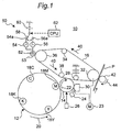
- Fig. 1 is a schematic overall constructional view of an image forming apparatus
- Fig. 2 is an enlarged view of a toner collecting/charging device
- Fig. 3 is an enlarged perspective view of one end portion of a toner collecting/charging roller
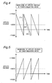
- Fig. 4 is a view showing a waveform of a first voltage for a toner-collecting mode
- Fig. 5 is a view showing a waveform of a second voltage for a toner-releasing mode
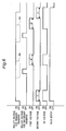
- Fig. 6 is a timing chart showing the toner-collecting and toner-releasing modes
- Figs. 7A to 7C are views showing waveforms of three-type modifications of the first voltage.
- Fig. 8 is a view showing a modification of a toner collecting/charging member.
- Fig. 1 is a schematic constructional view of an image forming apparatus 10 which is an embodiment of the invention.
- Fig. 2 shows in enlargement a toner collecting/charging device 50 in Fig. 1 .
- the image forming apparatus 10 includes a developing unit (image forming section) 12, a photoconductor (image carrier) 14, and an intermediate transfer belt (transfer member) 16. It is noted that the transfer member is not limited to a belt, and may be given in other forms (e.g., a drum).
- the developing unit 12 includes four developing devices 18Y, 18M, 18C, 18K corresponding to four-color toners (developers) cyan (C), magenta (M), yellow (Y), black (K) in a circumferentially arrayed state.
- the developing unit 12 can be driven into rotation in a direction indicated by an arrow 20 (as well as in a direction opposite to this direction). From a developing device that has come to a development position facing the photoconductor 14 as a result of rotation of the developing unit 12, toner is fed so as to be deposited by electrostatic force onto an electrostatic latent image formed on a surface of the photoconductor 14, by which a toner image is formed.
- the normal polarity for the toner used in this embodiment is assumed to be the negative polarity, yet the present invention is applicable also to toners of which the normal polarity is the positive polarity.
- the photoconductor 14 which is a well-known one having a photoconductive layer on a surface of a drum-shaped base body, can be driven by a main motor 23 into rotation in a direction indicated by an arrow 22.
- a charging device 24 for uniformly charging the surface of the photoconductor 14 to, e.g.
- an exposure device 26 for exposing the surface of the uniformly charged photoconductor 14 to laser light to form an electrostatic latent image composed of voltage decayed portions (e.g., -50 V), a primary transfer roller (primary transfer section) 28 which is provided in adjacency to the photoconductor 14 with the intermediate transfer belt 16 interposed therebetween and to which a primary transfer bias is applied, and a cleaning device (cleaning section) 30 for, after primary transfer of a toner image onto the intermediate transfer belt 16 by an electrostatic action of the primary transfer roller, scraping and collecting toner remaining on the photoconductor 14.
- a primary transfer roller primary transfer section
- the intermediate transfer belt 16 which is an endless belt made of resin film as an example, is driven into rotation in a direction indicated by an arrow 40 as, for example, a roller 32 is driven by the main motor 23 while the intermediate transfer belt 16 is supported by outer peripheral portions of five rollers 28, 32, 34, 36, 38, including the primary transfer roller 28, placed inside.
- a secondary transfer roller (secondary transfer section) 42 to which a secondary transfer bias is applied by an unshown power supply is rotatably pressed on a surface portion of the intermediate transfer belt 16 which is on the downstream side of the photoconductor 14 and which is supported by the roller 32.
- a contact portion between this secondary transfer roller 42 and the intermediate transfer belt 16 serves as a secondary transfer site.
- a toner image primarily transferred to the intermediate transfer belt 16 is secondarily transferred by electrostatic action of a secondary transfer roller 44 onto a sheet P as a recording medium to be introduced to the secondary transfer site at a specified timing.
- a toner collecting/charging device (developer collecting/charging device) 50 is provided in adjacency to a surface portion of the intermediate transfer belt 16 supported by the roller 36.
- the toner collecting/charging device 50 includes: a rotatable toner collecting/charging roller (developer collecting/charging member) 52 which is provided in such close proximity to the intermediate transfer belt 16 as not to make contact with the primarily transferred toner image and which has a collecting function of temporarily collecting after-transfer remaining toner remaining on the intermediate transfer belt 16 after secondary transfer and a charging function of charging the after-transfer remaining toner to a specified polarity; a first AC power supply 54 (second power supply) and a second AC power supply (third power supply) 56 electrically connected to the toner collecting/charging roller 52; a selector switch 58 which is to be switched between first, second terminal portions 54a, 56a connected to the first, second AC power supplies 54, 56, respectively; and a DC power supply (first power supply) 60 connected to the selector switch 58.
- the selector switch 58 is changed over based on a signal inputted from a CPU 62. Also, the selector switch 58, as shown by broken line in Fig. 2 , can be set in a neutral position where it makes contact with neither of the terminal portions 54a, 56a. In addition, in this embodiment, the selector switch 58 and the CPU 62 constitute a control section of this invention.
- a first voltage in which the first AC voltage by the first AC power supply 54 is superimposed on the DC voltage by the DC power supply 60 is applied when the selector switch 58 is brought into contact with the first terminal portion 54a
- a second voltage in which the second AC voltage by the second AC power supply 56 is superimposed on the DC voltage by the DC power supply 60 is applied when the selector switch 58 is brought into contact with the second terminal portion 56a.
- waveform of the first AC voltage and waveform of the second AC voltage are shaped different from each other, details of which will be described later.
- toner-collecting mode a state in which the first voltage is applied to the toner collecting/charging roller 52
- toner-releasing mode a state in which the second voltage is applied to the toner collecting/charging roller 52
- the first voltage and the second voltage are applied by using two AC power supplies 54, 56 that generate AC voltages different in waveform from each other.
- one high-voltage transformer which can be controlled by software for voltage value, waveform, frequency, duty ratio and the like may be used to generate the first voltage and the second voltage based on a voltage value and a waveform stored in memory of the control section.
- the toner collecting/charging roller 52 is a cylindrical-shaped roller made of a semiconductive material of, e.g., about 10 7 - 10 8 ⁇ and, more specifically, it may be formed by coating an outer peripheral surface of a metallic-cylinder cored bar with semiconductive rubber (e.g., EPDM (Ethylene Propylene Diene Monomer)).
- semiconductive rubber e.g., EPDM (Ethylene Propylene Diene Monomer)
- PET film rings 53 each having a thickness of, e.g., 150 ⁇ m are affixed, respectively.
- These film rings 53 are set in contact with both side portions of the intermediate transfer belt 16 corresponding to non-image-formation regions, respectively, so that the toner collecting/charging roller 52 is provided in proximity to the intermediate transfer belt 16, but with a distance d of 150 ⁇ m corresponding to the thickness of each film ring 53 provided from the intermediate transfer belt 16.
- the distance d although exemplified by 150 ⁇ m above, is yet preferably not less than 20 ⁇ m for the purpose of avoiding contact with a plural-color toner image that is to be primarily transferred onto the intermediate transfer belt 16 in superimposition during the image formation, while the distance d is preferably set not more than 200 ⁇ m, which is a distance at which relatively uniform discharge is generated between the toner collecting/charging roller 52 and the intermediate transfer belt 16 even in any environmental conditions from low-temperature, low-humidity to high-temperature, high humidity conditions, as will be described in conjunction with later-described cleaning operations.
- an AC voltage V p-p contained in the voltage applied to the toner collecting/charging roller 52 for generation of discharge in a most proximal portion (i.e., in the space of the distance d) between the toner collecting/charging roller 52 and the intermediate transfer belt 16 is, preferably, a value that satisfies that V p-p > 2x(6.2d+312).
- the intermediate transfer belt 16 which is a resistive material, has a potential, values lower than those which satisfy the foregoing conditional equation may be used for the AC voltage value.
- the CPU 62 When color image data is inputted to the CPU 62 together with a print command from an external unit such as a personal computer or the like, the CPU 62 performs data development process of color image data into Y, M, C, K color data, and outputs a signal to the exposure device 26 to instruct on laser exposure of the photoconductor 14 based on these individual color data.
- the surface of the photoconductor 14 driven into rotation in the direction of the arrow 22 is uniformly charged by the charging device 24 to, for example, -600 V, and the surface of the uniformly charged photoconductor is exposed to laser light based on cyan data by the exposure device 26, by which an electrostatic latent image formed of a voltage decayed portion of, e.g., -50 V is formed.
- the developing device 18C has been located at the development position, by which cyan toner is fed to the electrostatic latent image on the photoconductor surface so that a cyan toner image is formed.
- This cyan toner image is primarily transferred from the photoconductor 14 to the intermediate transfer belt 16. It is noted that toner remaining on the photoconductor 14 after the primary transfer is collected by the cleaning device 30.
- magenta, yellow and black, toner images are formed, respectively, by similar process one after another, and primarily transferred from the photoconductor 14 to the intermediate transfer belt 16 in superimposition one after another.
- the toner collecting/charging roller 52 is positioned in proximity to the intermediate transfer belt 16 with a specified gap thereto. Therefore, the toner collecting/charging roller 52 is prevented from contacting and disturbing the toner image on the intermediate transfer belt 16 during the image formation.
- the four-color toner images primarily transferred on the intermediate transfer belt 16 in the way described above are secondarily transferred collectively onto the sheet P introduced to the secondary transfer site at a specified timing from below. Thereafter, the sheet P, after having the toner image melted and fixed thereto during passage through the fixing unit, is discharged outside the image forming apparatus (e.g., into a discharged paper tray provided on the top or side face).
- the selector switch 58 is kept at a neutral position where it is in contact with neither of the terminal portions 54a, 56a, so that no voltage is applied to the toner collecting/charging roller 52.
- the selector switch 58 is switched so as to come into contact with either of the terminal portions 54a, 56a, so that a toner-collecting mode or a toner-releasing mode is executed.
- the toner-collecting mode keeps executed during a period from completion of a secondary transfer to a primary transfer of a next-printing-object image onto the intermediate transfer belt 16, and, without no next image, from the secondary transfer to expiration of a specified time.
- the toner-releasing mode is executed at a start time (when the image forming apparatus is powered on for start-up) and at an end sequence time (when no image to be next printed is present upon termination of a sequence of image forming operations).
- the toner-releasing mode is executed after the toner-collecting mode is executed from the secondary transfer to expiration of the specified time under the condition that no image to be next printed is present.
- the toner-collecting mode is executed after a four-color toner image on the intermediate transfer belt 16 is secondarily transferred onto the sheet P, by which part of the after-transfer remaining toner on the intermediate transfer belt 16 is collected.
- the selector switch 58 is switched to a state in which it is in contact with the first terminal portion 54a, by which the first voltage is applied to the toner collecting/charging roller 52.
- Fig. 4 shows a waveform of the first voltage as a concrete example.
- This first voltage is a voltage in which a first AC voltage of a sawtooth waveform having a value of Vp-p, 2800 V, and a frequency of 1250 Hz by the first AC power supply 54 is superimposed on a DC voltage of +300 V by the DC power supply 60.
- the frequency given as 1250 Hz above, depends on the process speed (125 mm/sec. in this embodiment) of the image forming apparatus 10, and is preferably set so as to satisfy that process speed (mm/sec.) / frequency (Hz) ⁇ 1 (mm).
- the waveform of the first voltage is a sawtooth-shaped one in which rise time and fall time differ from each other. Specifically, the rise time is set relatively short and the fall time is set relatively long and, more specifically, the voltage value rises instantly from -1100 V to +1700 V at a rising section, and relatively slowly changes from +1700 V to -1100 V at a falling section.
- the waveform of the first voltage is characterized by an abrupt change in the transition from the voltage of -1100 V of the same polarity as the toner that forms the image, to the voltage of +1700 V of the same polarity, and by a slow change in the transition from the voltage of +1700 V of the reverse polarity to the toner that forms the image, to the voltage of -1100 V of the same polarity.
- the after-transfer remaining toner is partly collected by the toner collecting/charging roller 52, thus being decreased in quantity.
- the after-transfer remaining toner passing through the region opposed to the toner collecting/charging roller 52 can be put into a positively charged state, which is of the reverse polarity to the normal polarity, with higher reliability.
- the strength of the electric field formed therebetween also weakens gradually until such a discharge as described above no longer occurs.
- the position where the discharge comes not to occur any more is still quite proximate to the toner collecting/charging roller 52, so that the after-transfer remaining toner is charged to a positive voltage together with the surface of the intermediate transfer belt 16, which is a resistive material, by the action of the DC voltage of +300 V contained in the first voltage.
- the after-transfer remaining toner positively charged by the toner collecting/charging roller 52 in the way described above is moved to a position of contact with the photoconductor 14 along with the rotation of the intermediate transfer belt 16 and, at that position, electrically adsorbed and thus reversely transferred to the photoconductor 14 having the surface voltage of -600 V except its electrostatic latent image portion, thereafter being collected by the cleaning device 30.
- the CPU 62 switches the selector switch 58 into contact with the second terminal portion 56a.
- the second voltage is applied to the toner collecting/charging roller 52, by which the toner-releasing mode is executed.
- Fig. 5 shows a waveform of the second voltage as a concrete example.
- This second voltage is a voltage in which a second AC voltage of a sawtooth waveform having a value of V P-P , 2800 V, and a frequency of 1250 Hz by the second AC power supply 56 is superimposed on a DC voltage of +300 V by the DC power supply 60.
- the waveform of this second AC voltage also is a sawtooth-shaped one in which rise time and fall time differ from each other, but has a waveform different from that of the first AC voltage.
- the waveform of the second voltage is such that the rise time is set relatively long and the fall time is set relatively short, and that the voltage value rises slowly from -1100 V to +1700 V at a rising section, and instantly changes from +1700 V to -1100 V at a falling section.
- the waveform of the second voltage is characterized by a slow change in the transition from the voltage of -1100 V of the same polarity as the toner that forms the image, to the voltage of +1700 V of the same polarity, and by an abrupt change in the transition from the voltage of +1700 V of the reverse polarity to the toner that forms the image, to the voltage of -1100 V of the same polarity.
- the after-transfer remaining toner temporarily collected during image formation is released from the toner collecting/charging roller 52 onto the intermediate transfer belt 16 by an action reverse to that in the image formation, and moved to a position of contact with the photoconductor 14 along with the rotation of the intermediate transfer belt 16 in a state that the after-transfer remaining toner is positively charged by an action similar to that for the first voltage. Then, at that position, the after-transfer remaining toner is electrically adsorbed and thus reversely transferred to the photoconductor 14 having the surface voltage of -600 V except its electrostatic latent image portion, and thereafter collected by the cleaning device 30.
- the main motor 23 When a print signal is inputted to the image forming apparatus 10, the main motor 23 is turned on so that the photoconductor 14, the intermediate transfer belt 16 and the like are started to be rotationally driven, while the primary transfer roller voltage is turned on, so that a toner image formed on the photoconductor 14 can be primarily transferred onto the photoconductor 14.
- the second voltage is applied for a specified time period t1.
- the reason for applying the second voltage of the toner-releasing mode is that the after-transfer remaining toner, if it has been kept temporarily collected to the toner collecting/charging roller 52 at a time of printing of the preceding job, is released onto the intermediate transfer belt 16 so as to be collected by the cleaning device 30 via the photoconductor 14.
- the secondary transfer roller voltage is applied to the secondary transfer roller 42, by which the four-color toner image is secondarily transferred onto the sheet P.
- the primary transfer voltage is kept turned off during an interval from an end of the primary transfer of the four-color toner image onto the intermediate transfer belt 16 to execution of primary transfer for a next image as shown by broken line 64 in Fig. 6 .
- the primary transfer voltage is kept turned on even during a time zone between one image and another in order that the toner released to the intermediate transfer belt 16 at an end sequence of the preceding printing can reliably be reversely transferred and collected to the photoconductor 14, as described above.
- the first voltage is turned on, and kept as it is for a specified time period t2, at a timing when the region with the after-transfer remaining toner present thereon has almost reached a position opposed to the toner collecting/charging roller 52 along with the rotation of the intermediate transfer belt 16, during which the toner-collecting mode is executed.
- the specified time period t2 is, preferably, longer than at least the time required for the intermediate transfer belt 16 to turn around by one cycle. The reason of this is to allow the collection of the after-transfer remaining toner via the photoconductor 14 to be reliably carried out all around the intermediate transfer belt 16.
- the applied voltage to the toner collecting/charging roller 52 is switched to the second voltage, which is kept applied for the specified time period t1 while the toner-releasing mode is executed.
- the toner-releasing mode is executed before the image forming apparatus is halted (put into a standby state) so that the after-transfer remaining toner primarily collected to the toner collecting/charging roller 52 is collected via the intermediate transfer belt 16 and the photoconductor 14.
- first print time which is the time elapsing from reception of a next-job print command until output of a first-sheet image.
- the main motor 23 In synchronization with an end of the toner-releasing mode, the main motor 23 is turned off so that the image forming apparatus 10 is halted.
- the primary transfer roller voltage although preferably kept turned on to collect the after-transfer remaining toner remaining on the intermediate transfer belt 16 to the photoconductor 14, is turned off earlier than a motor halt (more accurately, turn-off of the charging device 24) so as not to cause transfer memory to the photoconductor 14 due to the primary transfer bias.
- both collection and release of the after-transfer remaining toner by the toner collecting/charging roller 52 are performed before the image forming apparatus is halted.
- the apparatus may be halted after only the collection of the after-transfer remaining toner is performed, after which the release of the after-transfer remaining toner may be done at a time point when a next print signal is inputted.
- the image forming apparatus may be halted as it is, after which collection and release of the after-transfer remaining toner may be done at a time point when a next print command is inputted.
- the toner collecting/charging roller 52 is provided in such proximity to the intermediate transfer belt 16 as not to make contact with a primarily transferred toner image, and therefore never contacts or disturbs the primarily transferred toner image during the image formation. As a result, there is no need for providing a contact-and-separation drive mechanism for the toner collecting/charging roller 52, contributing to scale-down and cost reduction of the image forming apparatus 10.
- the after-transfer remaining toner that has decreased in its remaining amount can be positively charged to a polarity reverse to a normal polarity with reliability.
- the after-transfer remaining toner can be reversely transferred from the intermediate transfer belt 16 to the photoconductor 14, thus being collected, with high reliability.
- the waveform of the first voltage shown in Fig. 4 to be used in the toner-collecting mode has been so assumed that its rising section and falling section are given each in the form of one straight line, but may be so formed that the rising section and the falling section are different in waveform shape from each other.
- the waveform is preferably so set that the region indicated by (2) in Fig. 4 has more negative-side portion as much as possible in time base with a view to allowing for longer time to be taken for moving the toner to the toner collecting/charging roller.
- the falling section may be set constant on the negative side of +300 V over the region (2) as shown in Fig.
- the falling section has a point of inflection near an about zero-volt point in the region (2) as shown in 7B, or the falling section may be so formed as to be curved up to about the lower limit of the region (2) as shown in Fig. 7C .
- waveforms obtained by inverting the waveforms shown in Fig. 7A - 7C , respectively, up and down on a center of +300 V are those of the second voltage for the toner-releasing mode.
- control for changing the values of V p-p for the first and second voltages may be performed based on a temperature and a humidity detected by these sensors. For example, it is permissible that the value of V p-p is set smaller than a normal one under high temperature and high humidity conditions in which discharge is more likely to occur, while, conversely, the value of Vp-p is set larger than the normal one under low temperature and low humidity conditions in which discharge is less likely to occur.
- the toner collecting/charging member is not limited to roller-shaped ones, and may be provided in other shapes.
- a curved plate-shaped toner collecting/charging member 70 may be used.
- the toner collecting/charging member 70 has a two-layered structure of a resistive layer 72 facing the intermediate transfer belt 16, and a conductive layer 74 provided on its rear surface.
Landscapes
- Physics & Mathematics (AREA)
- General Physics & Mathematics (AREA)
- Electrostatic Charge, Transfer And Separation In Electrography (AREA)
- Dry Development In Electrophotography (AREA)
- Control Or Security For Electrophotography (AREA)
- Color Electrophotography (AREA)
Claims (6)
- Reinigungsverfahren für Entwickler, der nach der Übertragung auf einem Übertragungselement (16) verbleibt, nachdem ein Entwicklerbild, das von einem Bildträger (1) primär auf das Übertragungselement übertragen wird, sekundär auf ein Aufzeichnungsmedium (P) übertragen wurde, wobei das Verfahren die Schritte aufweist:Anlegen einer bestimmten Spannung an den nach der Übertragung verbleibenden Entwickler über ein Entwickler-Aufnahme/Ladungs-Element (52), das in solcher Nähe zum Übertragungselement angeordnet ist, dass dieses nicht mit dem primär übertragenen Entwicklerbild in Kontakt steht, so dass der nach der Übertragung verbleibende Entwickler vorübergehend durch das Entwickler-Aufnahme/Ladungs-Element aufgenommen wird und ferner auf eine bestimmte Polarität geladen wird;danach umgekehrt Übertragen des nach der Übertragung verbleibenden Entwicklers auf den Bildträger und anschließend Aufnehmen des nach der Übertragung verbleibenden Entwicklers, wobeidie bestimmte Spannung eine Spannung ist, bei der eine Wechselspannung einer Gleichspannung überlagert wird und eine Wellenform der Wechselspannung so geändert wird, dass das Entwickler-Aufnahme/Ladungs-Element zwischen einem Entwickleraufnahmemodus, durch den ein Teil des nach der Übertragung verbleibenden Toners auf dem Übertragungselement aufgenommen wird, wobei der Entwickleraufnahmemodus eine erste Wechselspannung hat, die eine erste Wellenform mit einer relativ kurzen Anstiegszeit und einer relativ langen Abfallzeit hat, und einem Entwicklerabgabemodus umgeschaltet wird, durch den der nach der Übertragung verbleibende Toner von dem Aufnahmeladungselement auf das Übertragungselement abgegeben wird, wobei der Entwicklerabgabemodus eine zweite Wechselspannung hat, die eine zweite Wellenform mit einer relativ langen Anstiegszeit und einer relativ kurzen Abfallzeit hat.
- Bildausbildungsvorrichtung, die aufweist:einen Bildträger (14), der drehbar betätigt wird;einen Bildausbildungsabschnitt (12) zum Ausbilden eines Entwicklerbilds auf dem Bildträger;ein Übertragungselement (16), das in Kontakt mit dem Bildträger gedreht wird;einen primären Übertragungsabschnitt, der gegenüber dem Bildträger vorgesehen ist, wobei das Übertragungselement dazwischen vorgesehen ist, und der ein Entwicklerbild von dem Bildträger zum Übertragungselement überträgt;einen Reinigungsabschnitt (30) zum Aufnehmen von Entwickler, der auf dem Bildträger nach der primären Übertragung verbleibt;einen sekundären Übertragungsabschnitt, der in einer Drehrichtung des Übertragungselements auf einer stromabwärtsgelegenen Seite des primären Übertragungsabschnitts angeordnet ist und der ein Entwicklerbild von dem Übertragungselement auf ein Aufzeichnungsmedium sekundär überträgt;eine Rolle (52), die auf einer stromabwärts gelegenen Seite des sekundären Übertragungsabschnitts in der Drehrichtung des Übertragungselements angeordnet ist und die mit einem solchen Abstand zum Übertragungselement festgelegt ist, dass diese nicht mit dem Entwicklerbild, das auf das Übertragungselement übertragen wird, in Kontakt steht;eine erste Leistungszufuhr (60), die vorgesehen ist, um eine Gleichspannung derselben Polarität wie der Entwickler, der ein Bild auf dem Bildträger ausbildet, an die Rolle anzulegen;eine zweite Leistungszufuhr (54), die vorgesehen ist, um eine erste Wechselspannung, die eine erste Wellenform mit einer relativ kurzen Anstiegszeit und einer relativ langen Abfallzeit hat, an die Rolle anzulegen;eine dritte Leistungszufuhr (56), die vorgesehen ist, um eine zweite Wechselspannung, die eine zweite Wellenform mit einer relativ langen Anstiegszeit und einer relativ kurzen Abfallzeit aufweist, an die Rolle anzulegen; undeinen Steuerabschnitt (62), der vorgesehen ist, um zwischen der zweiten und dritten Leistungszufuhr umzuschalten, so dass, nachdem an die Rolle angelegte Spannungen von der ersten Leistungszufuhr und der zweiten Leistungszufuhr für eine bestimmte Zeitdauer beibehalten wurden, an die Rolle angelegte Spannungen von der ersten Leistungszufuhr und der dritten Leistungszufuhr für eine bestimmte Zeitdauer beibehalten werden.
- Bildausbildungsvorrichtung nach Anspruch 2, bei der die bestimmte Zeitdauer, in der an die Rolle angelegte Spannungen von der ersten Leistungszufuhr und der zweiten Leistungszufuhr beibehalten werden, wenigstens länger als eine Zeitdauer ist, die das Übertragungselement für eine Umdrehung benötigt.
- Bildausbildungsvorrichtung nach Anspruch 2 oder 3, bei der, nachdem ein Entwicklerbild zum Aufzeichnungsmedium mittels des sekundären Übertragungsabschnitts übertragen wurde, der Steuerabschnitt vorgesehen ist, um eine solche Steuerung durchzuführen, dass Spannungen von der ersten Leistungszufuhr und der zweiten Leistungszufuhr für eine bestimmte Zeitdauer an die Rolle angelegt werden und danach Spannungen von der ersten Leistungszufuhr und der dritten Leistungszufuhr für ein bestimmte Zeitdauer an die Rolle angelegt werden.
- Bildausbildungsvorrichtung nach einem der Ansprüche 2 bis 4, bei der eine Wellenform der Wechselspannung, die von der zweiten Leistungszufuhr angelegt wird, durch eine abrupte Änderung der Spannung bei einem Übergang von der Spannung derselben Polarität wie die des Entwicklers, der das Bild ausbildet, zur Spannung der umgekehrten Polarität und durch eine geringe Änderung der Spannung bei einem Übergang von der Spannung der umgekehrten Polarität zur Spannung derselben Polarität wie der des Entwicklers, der das Bild ausbildet, charakterisiert ist.
- Bildausbildungsvorrichtung nach Anspruch 5, bei der die Wellenform der Wechselspannung, die durch die dritte Leistungszufuhr angelegt wird, durch eine abrupte Änderung der Spannung bei einem Übergang von der Spannung der umgekehrten Polarität bezüglich der des Entwicklers, der das Bild ausbildet, zur Spannung derselben Polarität und durch eine geringe Änderung der Polarität bei einem Übergang von der Spannung derselben Polarität wie die des Entwicklers, der das Bild ausbildet, zur Spannung der umgekehrten Polarität charakterisiert ist.
Applications Claiming Priority (1)
| Application Number | Priority Date | Filing Date | Title |
|---|---|---|---|
| JP2007147952A JP4375441B2 (ja) | 2007-06-04 | 2007-06-04 | 現像剤回収帯電部材、画像形成装置、およびクリーニング方法 |
Publications (2)
| Publication Number | Publication Date |
|---|---|
| EP2000863A1 EP2000863A1 (de) | 2008-12-10 |
| EP2000863B1 true EP2000863B1 (de) | 2014-03-19 |
Family
ID=39731305
Family Applications (1)
| Application Number | Title | Priority Date | Filing Date |
|---|---|---|---|
| EP08010119.9A Ceased EP2000863B1 (de) | 2007-06-04 | 2008-06-03 | Bilderzeugungsvorrichtung und Reinigungsverfahren |
Country Status (4)
| Country | Link |
|---|---|
| US (1) | US8041249B2 (de) |
| EP (1) | EP2000863B1 (de) |
| JP (1) | JP4375441B2 (de) |
| CN (1) | CN101320250B (de) |
Families Citing this family (6)
| Publication number | Priority date | Publication date | Assignee | Title |
|---|---|---|---|---|
| JP5595226B2 (ja) | 2010-10-29 | 2014-09-24 | キヤノン株式会社 | 画像形成装置 |
| JP5888588B2 (ja) * | 2010-11-19 | 2016-03-22 | 株式会社リコー | 転写装置及び画像形成装置 |
| JP5936109B2 (ja) | 2011-12-06 | 2016-06-15 | 株式会社リコー | 転写装置及びこれを用いる画像形成装置 |
| JP5987864B2 (ja) * | 2014-06-03 | 2016-09-07 | コニカミノルタ株式会社 | 画像形成装置 |
| JP6245232B2 (ja) * | 2015-08-05 | 2017-12-13 | コニカミノルタ株式会社 | 画像形成装置、画像形成システムおよび滑剤量調整方法 |
| JP6632292B2 (ja) * | 2015-09-25 | 2020-01-22 | キヤノン株式会社 | 画像形成装置 |
Family Cites Families (10)
| Publication number | Priority date | Publication date | Assignee | Title |
|---|---|---|---|---|
| JPH08137204A (ja) * | 1994-11-09 | 1996-05-31 | Minolta Co Ltd | 画像形成装置 |
| DE69625542T2 (de) * | 1995-05-23 | 2003-10-02 | Canon K.K., Tokio/Tokyo | Bilderzeugungsgerät und Methode mit einem Zwischenübertragungselement |
| US5752130A (en) * | 1995-07-07 | 1998-05-12 | Canon Kabushiki Kaisha | Image forming apparatus for cleaning residual toner from an intermediate transfer member |
| JPH09197764A (ja) | 1996-01-12 | 1997-07-31 | Canon Inc | 画像形成装置 |
| JP3466825B2 (ja) | 1996-08-07 | 2003-11-17 | キヤノン株式会社 | クリーニング装置 |
| JP3733249B2 (ja) * | 1998-09-12 | 2006-01-11 | キヤノン株式会社 | 画像形成装置 |
| JP2003005494A (ja) | 2001-06-21 | 2003-01-08 | Canon Inc | 帯電装置、画像形成装置及びプロセスカートリッジ |
| JP3634840B2 (ja) | 2002-12-24 | 2005-03-30 | キヤノン株式会社 | 画像形成装置 |
| JP4708924B2 (ja) * | 2005-09-01 | 2011-06-22 | キヤノン株式会社 | 画像形成装置 |
| JP2007147952A (ja) | 2005-11-28 | 2007-06-14 | Konica Minolta Opto Inc | 撮像光学系位置調整方法 |
-
2007
- 2007-06-04 JP JP2007147952A patent/JP4375441B2/ja not_active Expired - Fee Related
-
2008
- 2008-06-03 US US12/132,418 patent/US8041249B2/en not_active Expired - Fee Related
- 2008-06-03 EP EP08010119.9A patent/EP2000863B1/de not_active Ceased
- 2008-06-04 CN CN200810099753.7A patent/CN101320250B/zh active Active
Also Published As
| Publication number | Publication date |
|---|---|
| US8041249B2 (en) | 2011-10-18 |
| EP2000863A1 (de) | 2008-12-10 |
| CN101320250B (zh) | 2015-07-22 |
| US20080298832A1 (en) | 2008-12-04 |
| CN101320250A (zh) | 2008-12-10 |
| JP4375441B2 (ja) | 2009-12-02 |
| JP2008299251A (ja) | 2008-12-11 |
Similar Documents
| Publication | Publication Date | Title |
|---|---|---|
| US8027612B2 (en) | Image forming apparatus having a charge member disposed near an image bearing member | |
| EP2000863B1 (de) | Bilderzeugungsvorrichtung und Reinigungsverfahren | |
| JP3619140B2 (ja) | 画像形成装置 | |
| JP2001166558A (ja) | 画像形成装置 | |
| US20050232668A1 (en) | Imaging forming apparatus | |
| US20080118272A1 (en) | Image forming apparatus | |
| JP4684617B2 (ja) | 画像形成装置 | |
| US8160480B2 (en) | Image forming apparatus having controlled speed differential between image bearing members and intermediate transfer belt | |
| JP3907293B2 (ja) | 画像形成装置 | |
| JP4089417B2 (ja) | 画像形成装置、および画像形成装置の制御方法 | |
| JPH11311906A (ja) | 画像形成装置 | |
| US8831453B2 (en) | Image forming apparatus | |
| CN102981389A (zh) | 图像形成设备 | |
| JP2004198557A (ja) | 画像形成装置、および像坦持体の保持方法 | |
| US8892003B2 (en) | Image forming apparatus | |
| JP2006163301A (ja) | 画像形成装置 | |
| JP2006313316A (ja) | 画像形成装置 | |
| JP2005338700A (ja) | 画像形成装置 | |
| JP4207472B2 (ja) | 画像形成装置 | |
| JP3351169B2 (ja) | 画像形成装置 | |
| JP3583381B2 (ja) | カラー電子写真装置 | |
| JP2018146897A (ja) | 電源装置及び画像形成装置 | |
| JPH11316532A (ja) | 画像形成装置 | |
| JPH05224574A (ja) | 画像形成装置 | |
| JP2005043627A (ja) | 画像形成装置 |
Legal Events
| Date | Code | Title | Description |
|---|---|---|---|
| PUAI | Public reference made under article 153(3) epc to a published international application that has entered the european phase |
Free format text: ORIGINAL CODE: 0009012 |
|
| AK | Designated contracting states |
Kind code of ref document: A1 Designated state(s): AT BE BG CH CY CZ DE DK EE ES FI FR GB GR HR HU IE IS IT LI LT LU LV MC MT NL NO PL PT RO SE SI SK TR |
|
| AX | Request for extension of the european patent |
Extension state: AL BA MK RS |
|
| 17P | Request for examination filed |
Effective date: 20090610 |
|
| AKX | Designation fees paid |
Designated state(s): DE FR GB |
|
| 17Q | First examination report despatched |
Effective date: 20120620 |
|
| GRAP | Despatch of communication of intention to grant a patent |
Free format text: ORIGINAL CODE: EPIDOSNIGR1 |
|
| INTG | Intention to grant announced |
Effective date: 20131008 |
|
| GRAS | Grant fee paid |
Free format text: ORIGINAL CODE: EPIDOSNIGR3 |
|
| GRAA | (expected) grant |
Free format text: ORIGINAL CODE: 0009210 |
|
| AK | Designated contracting states |
Kind code of ref document: B1 Designated state(s): DE FR GB |
|
| REG | Reference to a national code |
Ref country code: GB Ref legal event code: FG4D |
|
| REG | Reference to a national code |
Ref country code: DE Ref legal event code: R096 Ref document number: 602008030926 Country of ref document: DE Effective date: 20140430 |
|
| REG | Reference to a national code |
Ref country code: DE Ref legal event code: R097 Ref document number: 602008030926 Country of ref document: DE |
|
| PLBE | No opposition filed within time limit |
Free format text: ORIGINAL CODE: 0009261 |
|
| STAA | Information on the status of an ep patent application or granted ep patent |
Free format text: STATUS: NO OPPOSITION FILED WITHIN TIME LIMIT |
|
| 26N | No opposition filed |
Effective date: 20141222 |
|
| REG | Reference to a national code |
Ref country code: DE Ref legal event code: R097 Ref document number: 602008030926 Country of ref document: DE Effective date: 20141222 |
|
| REG | Reference to a national code |
Ref country code: FR Ref legal event code: PLFP Year of fee payment: 9 |
|
| REG | Reference to a national code |
Ref country code: FR Ref legal event code: PLFP Year of fee payment: 10 |
|
| REG | Reference to a national code |
Ref country code: FR Ref legal event code: PLFP Year of fee payment: 11 |
|
| REG | Reference to a national code |
Ref country code: FR Ref legal event code: PLFP Year of fee payment: 16 |
|
| P01 | Opt-out of the competence of the unified patent court (upc) registered |
Effective date: 20230510 |
|
| PGFP | Annual fee paid to national office [announced via postgrant information from national office to epo] |
Ref country code: FR Payment date: 20240328 Year of fee payment: 17 |
|
| PGFP | Annual fee paid to national office [announced via postgrant information from national office to epo] |
Ref country code: GB Payment date: 20240402 Year of fee payment: 17 |
|
| PGFP | Annual fee paid to national office [announced via postgrant information from national office to epo] |
Ref country code: DE Payment date: 20240328 Year of fee payment: 17 |
|
| REG | Reference to a national code |
Ref country code: DE Ref legal event code: R119 Ref document number: 602008030926 Country of ref document: DE |
|
| GBPC | Gb: european patent ceased through non-payment of renewal fee |
Effective date: 20250603 |
|
| PG25 | Lapsed in a contracting state [announced via postgrant information from national office to epo] |
Ref country code: GB Free format text: LAPSE BECAUSE OF NON-PAYMENT OF DUE FEES Effective date: 20250603 |
|
| PG25 | Lapsed in a contracting state [announced via postgrant information from national office to epo] |
Ref country code: DE Free format text: LAPSE BECAUSE OF NON-PAYMENT OF DUE FEES Effective date: 20260101 |
|
| PG25 | Lapsed in a contracting state [announced via postgrant information from national office to epo] |
Ref country code: FR Free format text: LAPSE BECAUSE OF NON-PAYMENT OF DUE FEES Effective date: 20250630 |