EP1978571B1 - Dispositif électroluminescent organique et dispositif d'affichage - Google Patents
Dispositif électroluminescent organique et dispositif d'affichage Download PDFInfo
- Publication number
- EP1978571B1 EP1978571B1 EP08102434A EP08102434A EP1978571B1 EP 1978571 B1 EP1978571 B1 EP 1978571B1 EP 08102434 A EP08102434 A EP 08102434A EP 08102434 A EP08102434 A EP 08102434A EP 1978571 B1 EP1978571 B1 EP 1978571B1
- Authority
- EP
- European Patent Office
- Prior art keywords
- transporting
- layer
- charge
- organic electroluminescent
- light
- Prior art date
- Legal status (The legal status is an assumption and is not a legal conclusion. Google has not performed a legal analysis and makes no representation as to the accuracy of the status listed.)
- Expired - Fee Related
Links
- 229920000570 polyether Polymers 0.000 claims description 111
- 239000004721 Polyphenylene oxide Substances 0.000 claims description 110
- 239000000463 material Substances 0.000 claims description 78
- 150000002894 organic compounds Chemical class 0.000 claims description 39
- 125000003118 aryl group Chemical group 0.000 claims description 34
- 125000000217 alkyl group Chemical group 0.000 claims description 18
- 125000004432 carbon atom Chemical group C* 0.000 claims description 17
- 239000000758 substrate Substances 0.000 claims description 15
- 125000003710 aryl alkyl group Chemical group 0.000 claims description 13
- 238000002347 injection Methods 0.000 claims description 13
- 239000007924 injection Substances 0.000 claims description 13
- 150000002430 hydrocarbons Chemical class 0.000 claims description 12
- 125000004435 hydrogen atom Chemical group [H]* 0.000 claims description 11
- 150000004767 nitrides Chemical class 0.000 claims description 10
- 229910052809 inorganic oxide Inorganic materials 0.000 claims description 8
- 239000004215 Carbon black (E152) Substances 0.000 claims description 6
- XHCLAFWTIXFWPH-UHFFFAOYSA-N [O-2].[O-2].[O-2].[O-2].[O-2].[V+5].[V+5] Chemical compound [O-2].[O-2].[O-2].[O-2].[O-2].[V+5].[V+5] XHCLAFWTIXFWPH-UHFFFAOYSA-N 0.000 claims description 6
- 125000002252 acyl group Chemical group 0.000 claims description 6
- 229930195733 hydrocarbon Natural products 0.000 claims description 6
- 239000011159 matrix material Substances 0.000 claims description 6
- 229910000476 molybdenum oxide Inorganic materials 0.000 claims description 6
- PQQKPALAQIIWST-UHFFFAOYSA-N oxomolybdenum Chemical compound [Mo]=O PQQKPALAQIIWST-UHFFFAOYSA-N 0.000 claims description 6
- 125000001997 phenyl group Chemical group [H]C1=C([H])C([H])=C(*)C([H])=C1[H] 0.000 claims description 6
- 229910001935 vanadium oxide Inorganic materials 0.000 claims description 6
- 125000006267 biphenyl group Chemical group 0.000 claims description 2
- 125000003983 fluorenyl group Chemical group C1(=CC=CC=2C3=CC=CC=C3CC12)* 0.000 claims description 2
- 125000001624 naphthyl group Chemical group 0.000 claims description 2
- 239000010410 layer Substances 0.000 description 263
- 150000001875 compounds Chemical class 0.000 description 40
- -1 poly (p-phenylene vinylene) Polymers 0.000 description 37
- 239000002904 solvent Substances 0.000 description 36
- OKKJLVBELUTLKV-UHFFFAOYSA-N Methanol Chemical compound OC OKKJLVBELUTLKV-UHFFFAOYSA-N 0.000 description 27
- YXFVVABEGXRONW-UHFFFAOYSA-N Toluene Chemical compound CC1=CC=CC=C1 YXFVVABEGXRONW-UHFFFAOYSA-N 0.000 description 24
- 229920000642 polymer Polymers 0.000 description 23
- 239000000243 solution Substances 0.000 description 23
- MVPPADPHJFYWMZ-UHFFFAOYSA-N chlorobenzene Chemical compound ClC1=CC=CC=C1 MVPPADPHJFYWMZ-UHFFFAOYSA-N 0.000 description 22
- 238000000034 method Methods 0.000 description 19
- 230000000052 comparative effect Effects 0.000 description 17
- JKQOBWVOAYFWKG-UHFFFAOYSA-N molybdenum trioxide Chemical compound O=[Mo](=O)=O JKQOBWVOAYFWKG-UHFFFAOYSA-N 0.000 description 16
- UHOVQNZJYSORNB-UHFFFAOYSA-N Benzene Chemical compound C1=CC=CC=C1 UHOVQNZJYSORNB-UHFFFAOYSA-N 0.000 description 15
- 238000006243 chemical reaction Methods 0.000 description 15
- 239000012948 isocyanate Substances 0.000 description 14
- 239000000178 monomer Substances 0.000 description 14
- 238000001771 vacuum deposition Methods 0.000 description 14
- 238000001308 synthesis method Methods 0.000 description 13
- 125000006615 aromatic heterocyclic group Chemical group 0.000 description 12
- 229920001343 polytetrafluoroethylene Polymers 0.000 description 12
- 239000004810 polytetrafluoroethylene Substances 0.000 description 12
- YMWUJEATGCHHMB-UHFFFAOYSA-N Dichloromethane Chemical compound ClCCl YMWUJEATGCHHMB-UHFFFAOYSA-N 0.000 description 10
- 238000009835 boiling Methods 0.000 description 10
- 239000011521 glass Substances 0.000 description 10
- 238000010438 heat treatment Methods 0.000 description 10
- 238000004519 manufacturing process Methods 0.000 description 10
- 239000011248 coating agent Substances 0.000 description 9
- 238000000576 coating method Methods 0.000 description 9
- 239000006185 dispersion Substances 0.000 description 9
- 239000010408 film Substances 0.000 description 9
- 238000006116 polymerization reaction Methods 0.000 description 9
- XLYOFNOQVPJJNP-UHFFFAOYSA-N water Substances O XLYOFNOQVPJJNP-UHFFFAOYSA-N 0.000 description 9
- 239000004793 Polystyrene Substances 0.000 description 8
- 239000003054 catalyst Substances 0.000 description 8
- 230000002349 favourable effect Effects 0.000 description 8
- 125000002887 hydroxy group Chemical group [H]O* 0.000 description 8
- 229920002223 polystyrene Polymers 0.000 description 8
- VYPSYNLAJGMNEJ-UHFFFAOYSA-N Silicium dioxide Chemical compound O=[Si]=O VYPSYNLAJGMNEJ-UHFFFAOYSA-N 0.000 description 7
- WYURNTSHIVDZCO-UHFFFAOYSA-N Tetrahydrofuran Chemical compound C1CCOC1 WYURNTSHIVDZCO-UHFFFAOYSA-N 0.000 description 7
- 230000015572 biosynthetic process Effects 0.000 description 7
- 239000012212 insulator Substances 0.000 description 7
- 229920005547 polycyclic aromatic hydrocarbon Polymers 0.000 description 7
- 125000001424 substituent group Chemical group 0.000 description 7
- 238000003786 synthesis reaction Methods 0.000 description 7
- JUJWROOIHBZHMG-UHFFFAOYSA-N Pyridine Chemical compound C1=CC=NC=C1 JUJWROOIHBZHMG-UHFFFAOYSA-N 0.000 description 6
- ZMANZCXQSJIPKH-UHFFFAOYSA-N Triethylamine Chemical compound CCN(CC)CC ZMANZCXQSJIPKH-UHFFFAOYSA-N 0.000 description 6
- 238000005917 acylation reaction Methods 0.000 description 6
- 239000002585 base Substances 0.000 description 6
- 230000008569 process Effects 0.000 description 6
- YLQBMQCUIZJEEH-UHFFFAOYSA-N Furan Chemical compound C=1C=COC=1 YLQBMQCUIZJEEH-UHFFFAOYSA-N 0.000 description 5
- 229910019015 Mg-Ag Inorganic materials 0.000 description 5
- 239000002253 acid Substances 0.000 description 5
- 229910045601 alloy Inorganic materials 0.000 description 5
- 239000000956 alloy Substances 0.000 description 5
- 238000000151 deposition Methods 0.000 description 5
- 238000001035 drying Methods 0.000 description 5
- 229910052751 metal Inorganic materials 0.000 description 5
- 239000002184 metal Substances 0.000 description 5
- SMBBZHGTZJNSRQ-UHFFFAOYSA-N n'-(6,6-dichlorohexyl)methanediimine Chemical compound ClC(Cl)CCCCCN=C=N SMBBZHGTZJNSRQ-UHFFFAOYSA-N 0.000 description 5
- 230000001376 precipitating effect Effects 0.000 description 5
- 238000001556 precipitation Methods 0.000 description 5
- 239000000376 reactant Substances 0.000 description 5
- 238000004528 spin coating Methods 0.000 description 5
- 229910052720 vanadium Inorganic materials 0.000 description 5
- LEONUFNNVUYDNQ-UHFFFAOYSA-N vanadium atom Chemical compound [V] LEONUFNNVUYDNQ-UHFFFAOYSA-N 0.000 description 5
- OCJBOOLMMGQPQU-UHFFFAOYSA-N 1,4-dichlorobenzene Chemical compound ClC1=CC=C(Cl)C=C1 OCJBOOLMMGQPQU-UHFFFAOYSA-N 0.000 description 4
- IAZDPXIOMUYVGZ-UHFFFAOYSA-N Dimethylsulphoxide Chemical compound CS(C)=O IAZDPXIOMUYVGZ-UHFFFAOYSA-N 0.000 description 4
- XEEYBQQBJWHFJM-UHFFFAOYSA-N Iron Chemical compound [Fe] XEEYBQQBJWHFJM-UHFFFAOYSA-N 0.000 description 4
- UFWIBTONFRDIAS-UHFFFAOYSA-N Naphthalene Chemical compound C1=CC=CC2=CC=CC=C21 UFWIBTONFRDIAS-UHFFFAOYSA-N 0.000 description 4
- MWPLVEDNUUSJAV-UHFFFAOYSA-N anthracene Chemical compound C1=CC=CC2=CC3=CC=CC=C3C=C21 MWPLVEDNUUSJAV-UHFFFAOYSA-N 0.000 description 4
- 229910052799 carbon Inorganic materials 0.000 description 4
- 239000003795 chemical substances by application Substances 0.000 description 4
- 229940117389 dichlorobenzene Drugs 0.000 description 4
- ZUOUZKKEUPVFJK-UHFFFAOYSA-N diphenyl Chemical compound C1=CC=CC=C1C1=CC=CC=C1 ZUOUZKKEUPVFJK-UHFFFAOYSA-N 0.000 description 4
- 238000009826 distribution Methods 0.000 description 4
- 238000006266 etherification reaction Methods 0.000 description 4
- 239000000706 filtrate Substances 0.000 description 4
- NIHNNTQXNPWCJQ-UHFFFAOYSA-N fluorene Chemical compound C1=CC=C2CC3=CC=CC=C3C2=C1 NIHNNTQXNPWCJQ-UHFFFAOYSA-N 0.000 description 4
- 238000005227 gel permeation chromatography Methods 0.000 description 4
- 150000004820 halides Chemical class 0.000 description 4
- 125000000623 heterocyclic group Chemical group 0.000 description 4
- 229910052738 indium Inorganic materials 0.000 description 4
- 238000004020 luminiscence type Methods 0.000 description 4
- LQNUZADURLCDLV-UHFFFAOYSA-N nitrobenzene Chemical compound [O-][N+](=O)C1=CC=CC=C1 LQNUZADURLCDLV-UHFFFAOYSA-N 0.000 description 4
- 229910052757 nitrogen Inorganic materials 0.000 description 4
- IJGRMHOSHXDMSA-UHFFFAOYSA-N nitrogen Substances N#N IJGRMHOSHXDMSA-UHFFFAOYSA-N 0.000 description 4
- 229920005989 resin Polymers 0.000 description 4
- 239000011347 resin Substances 0.000 description 4
- 238000003756 stirring Methods 0.000 description 4
- GETQZCLCWQTVFV-UHFFFAOYSA-N trimethylamine Chemical compound CN(C)C GETQZCLCWQTVFV-UHFFFAOYSA-N 0.000 description 4
- JTPNRXUCIXHOKM-UHFFFAOYSA-N 1-chloronaphthalene Chemical compound C1=CC=C2C(Cl)=CC=CC2=C1 JTPNRXUCIXHOKM-UHFFFAOYSA-N 0.000 description 3
- ZWEHNKRNPOVVGH-UHFFFAOYSA-N 2-Butanone Chemical compound CCC(C)=O ZWEHNKRNPOVVGH-UHFFFAOYSA-N 0.000 description 3
- WFDIJRYMOXRFFG-UHFFFAOYSA-N Acetic anhydride Chemical compound CC(=O)OC(C)=O WFDIJRYMOXRFFG-UHFFFAOYSA-N 0.000 description 3
- OYPRJOBELJOOCE-UHFFFAOYSA-N Calcium Chemical compound [Ca] OYPRJOBELJOOCE-UHFFFAOYSA-N 0.000 description 3
- OKTJSMMVPCPJKN-UHFFFAOYSA-N Carbon Chemical compound [C] OKTJSMMVPCPJKN-UHFFFAOYSA-N 0.000 description 3
- LFQSCWFLJHTTHZ-UHFFFAOYSA-N Ethanol Chemical compound CCO LFQSCWFLJHTTHZ-UHFFFAOYSA-N 0.000 description 3
- UFHFLCQGNIYNRP-UHFFFAOYSA-N Hydrogen Chemical compound [H][H] UFHFLCQGNIYNRP-UHFFFAOYSA-N 0.000 description 3
- WHXSMMKQMYFTQS-UHFFFAOYSA-N Lithium Chemical compound [Li] WHXSMMKQMYFTQS-UHFFFAOYSA-N 0.000 description 3
- FYYHWMGAXLPEAU-UHFFFAOYSA-N Magnesium Chemical compound [Mg] FYYHWMGAXLPEAU-UHFFFAOYSA-N 0.000 description 3
- ZMXDDKWLCZADIW-UHFFFAOYSA-N N,N-Dimethylformamide Chemical compound CN(C)C=O ZMXDDKWLCZADIW-UHFFFAOYSA-N 0.000 description 3
- KWYUFKZDYYNOTN-UHFFFAOYSA-M Potassium hydroxide Chemical compound [OH-].[K+] KWYUFKZDYYNOTN-UHFFFAOYSA-M 0.000 description 3
- HEMHJVSKTPXQMS-UHFFFAOYSA-M Sodium hydroxide Chemical compound [OH-].[Na+] HEMHJVSKTPXQMS-UHFFFAOYSA-M 0.000 description 3
- 150000008065 acid anhydrides Chemical class 0.000 description 3
- 239000003377 acid catalyst Substances 0.000 description 3
- 125000003545 alkoxy group Chemical group 0.000 description 3
- 229910052782 aluminium Inorganic materials 0.000 description 3
- XAGFODPZIPBFFR-UHFFFAOYSA-N aluminium Chemical compound [Al] XAGFODPZIPBFFR-UHFFFAOYSA-N 0.000 description 3
- 125000003277 amino group Chemical group 0.000 description 3
- 125000004429 atom Chemical group 0.000 description 3
- 229910052788 barium Inorganic materials 0.000 description 3
- DSAJWYNOEDNPEQ-UHFFFAOYSA-N barium atom Chemical compound [Ba] DSAJWYNOEDNPEQ-UHFFFAOYSA-N 0.000 description 3
- 229910052791 calcium Inorganic materials 0.000 description 3
- 239000011575 calcium Substances 0.000 description 3
- 239000000975 dye Substances 0.000 description 3
- 229910052739 hydrogen Inorganic materials 0.000 description 3
- 239000001257 hydrogen Substances 0.000 description 3
- 230000006872 improvement Effects 0.000 description 3
- APFVFJFRJDLVQX-UHFFFAOYSA-N indium atom Chemical compound [In] APFVFJFRJDLVQX-UHFFFAOYSA-N 0.000 description 3
- 150000002513 isocyanates Chemical class 0.000 description 3
- 229910052744 lithium Inorganic materials 0.000 description 3
- 229910052749 magnesium Inorganic materials 0.000 description 3
- 239000011777 magnesium Substances 0.000 description 3
- 229910044991 metal oxide Inorganic materials 0.000 description 3
- 150000004706 metal oxides Chemical class 0.000 description 3
- 239000003960 organic solvent Substances 0.000 description 3
- 229920000553 poly(phenylenevinylene) Polymers 0.000 description 3
- 230000000379 polymerizing effect Effects 0.000 description 3
- 238000002360 preparation method Methods 0.000 description 3
- 239000011241 protective layer Substances 0.000 description 3
- UMJSCPRVCHMLSP-UHFFFAOYSA-N pyridine Natural products COC1=CC=CN=C1 UMJSCPRVCHMLSP-UHFFFAOYSA-N 0.000 description 3
- 238000011160 research Methods 0.000 description 3
- 239000000377 silicon dioxide Substances 0.000 description 3
- 238000004544 sputter deposition Methods 0.000 description 3
- 239000010409 thin film Substances 0.000 description 3
- TVIVIEFSHFOWTE-UHFFFAOYSA-K tri(quinolin-8-yloxy)alumane Chemical compound [Al+3].C1=CN=C2C([O-])=CC=CC2=C1.C1=CN=C2C([O-])=CC=CC2=C1.C1=CN=C2C([O-])=CC=CC2=C1 TVIVIEFSHFOWTE-UHFFFAOYSA-K 0.000 description 3
- JOYRKODLDBILNP-UHFFFAOYSA-N urethane group Chemical group NC(=O)OCC JOYRKODLDBILNP-UHFFFAOYSA-N 0.000 description 3
- CYSGHNMQYZDMIA-UHFFFAOYSA-N 1,3-Dimethyl-2-imidazolidinon Chemical compound CN1CCN(C)C1=O CYSGHNMQYZDMIA-UHFFFAOYSA-N 0.000 description 2
- 125000000094 2-phenylethyl group Chemical group [H]C1=C([H])C([H])=C(C([H])=C1[H])C([H])([H])C([H])([H])* 0.000 description 2
- CSCPPACGZOOCGX-UHFFFAOYSA-N Acetone Chemical compound CC(C)=O CSCPPACGZOOCGX-UHFFFAOYSA-N 0.000 description 2
- GYHNNYVSQQEPJS-UHFFFAOYSA-N Gallium Chemical compound [Ga] GYHNNYVSQQEPJS-UHFFFAOYSA-N 0.000 description 2
- VEXZGXHMUGYJMC-UHFFFAOYSA-N Hydrochloric acid Chemical compound Cl VEXZGXHMUGYJMC-UHFFFAOYSA-N 0.000 description 2
- CPLXHLVBOLITMK-UHFFFAOYSA-N Magnesium oxide Chemical compound [Mg]=O CPLXHLVBOLITMK-UHFFFAOYSA-N 0.000 description 2
- SECXISVLQFMRJM-UHFFFAOYSA-N N-Methylpyrrolidone Chemical compound CN1CCCC1=O SECXISVLQFMRJM-UHFFFAOYSA-N 0.000 description 2
- KDLHZDBZIXYQEI-UHFFFAOYSA-N Palladium Chemical compound [Pd] KDLHZDBZIXYQEI-UHFFFAOYSA-N 0.000 description 2
- ATUOYWHBWRKTHZ-UHFFFAOYSA-N Propane Chemical compound CCC ATUOYWHBWRKTHZ-UHFFFAOYSA-N 0.000 description 2
- KAESVJOAVNADME-UHFFFAOYSA-N Pyrrole Chemical compound C=1C=CNC=1 KAESVJOAVNADME-UHFFFAOYSA-N 0.000 description 2
- 229910052581 Si3N4 Inorganic materials 0.000 description 2
- XUIMIQQOPSSXEZ-UHFFFAOYSA-N Silicon Chemical compound [Si] XUIMIQQOPSSXEZ-UHFFFAOYSA-N 0.000 description 2
- PPBRXRYQALVLMV-UHFFFAOYSA-N Styrene Chemical compound C=CC1=CC=CC=C1 PPBRXRYQALVLMV-UHFFFAOYSA-N 0.000 description 2
- QAOWNCQODCNURD-UHFFFAOYSA-N Sulfuric acid Chemical compound OS(O)(=O)=O QAOWNCQODCNURD-UHFFFAOYSA-N 0.000 description 2
- YTPLMLYBLZKORZ-UHFFFAOYSA-N Thiophene Chemical compound C=1C=CSC=1 YTPLMLYBLZKORZ-UHFFFAOYSA-N 0.000 description 2
- GWEVSGVZZGPLCZ-UHFFFAOYSA-N Titan oxide Chemical compound O=[Ti]=O GWEVSGVZZGPLCZ-UHFFFAOYSA-N 0.000 description 2
- DTQVDTLACAAQTR-UHFFFAOYSA-N Trifluoroacetic acid Chemical compound OC(=O)C(F)(F)F DTQVDTLACAAQTR-UHFFFAOYSA-N 0.000 description 2
- HCHKCACWOHOZIP-UHFFFAOYSA-N Zinc Chemical compound [Zn] HCHKCACWOHOZIP-UHFFFAOYSA-N 0.000 description 2
- XLOMVQKBTHCTTD-UHFFFAOYSA-N Zinc monoxide Chemical compound [Zn]=O XLOMVQKBTHCTTD-UHFFFAOYSA-N 0.000 description 2
- PNEYBMLMFCGWSK-UHFFFAOYSA-N aluminium oxide Inorganic materials [O-2].[O-2].[O-2].[Al+3].[Al+3] PNEYBMLMFCGWSK-UHFFFAOYSA-N 0.000 description 2
- 230000004888 barrier function Effects 0.000 description 2
- 125000001797 benzyl group Chemical group [H]C1=C([H])C([H])=C(C([H])=C1[H])C([H])([H])* 0.000 description 2
- 230000005540 biological transmission Effects 0.000 description 2
- 239000004305 biphenyl Substances 0.000 description 2
- 235000010290 biphenyl Nutrition 0.000 description 2
- 238000005266 casting Methods 0.000 description 2
- 239000003153 chemical reaction reagent Substances 0.000 description 2
- 229910052681 coesite Inorganic materials 0.000 description 2
- 238000009833 condensation Methods 0.000 description 2
- 230000005494 condensation Effects 0.000 description 2
- 229910052802 copper Inorganic materials 0.000 description 2
- 239000010949 copper Substances 0.000 description 2
- 229910052906 cristobalite Inorganic materials 0.000 description 2
- 230000007423 decrease Effects 0.000 description 2
- 230000018044 dehydration Effects 0.000 description 2
- 238000006297 dehydration reaction Methods 0.000 description 2
- 125000001495 ethyl group Chemical group [H]C([H])([H])C([H])([H])* 0.000 description 2
- 239000007850 fluorescent dye Substances 0.000 description 2
- 229910052733 gallium Inorganic materials 0.000 description 2
- 230000009477 glass transition Effects 0.000 description 2
- 229910052737 gold Inorganic materials 0.000 description 2
- 239000010931 gold Substances 0.000 description 2
- 125000005843 halogen group Chemical group 0.000 description 2
- 125000001449 isopropyl group Chemical group [H]C([H])([H])C([H])(*)C([H])([H])[H] 0.000 description 2
- 229910052746 lanthanum Inorganic materials 0.000 description 2
- FZLIPJUXYLNCLC-UHFFFAOYSA-N lanthanum atom Chemical compound [La] FZLIPJUXYLNCLC-UHFFFAOYSA-N 0.000 description 2
- 239000011133 lead Substances 0.000 description 2
- PQXKHYXIUOZZFA-UHFFFAOYSA-M lithium fluoride Chemical compound [Li+].[F-] PQXKHYXIUOZZFA-UHFFFAOYSA-M 0.000 description 2
- 125000002496 methyl group Chemical group [H]C([H])([H])* 0.000 description 2
- 239000000203 mixture Substances 0.000 description 2
- PSHKMPUSSFXUIA-UHFFFAOYSA-N n,n-dimethylpyridin-2-amine Chemical compound CN(C)C1=CC=CC=N1 PSHKMPUSSFXUIA-UHFFFAOYSA-N 0.000 description 2
- QJGQUHMNIGDVPM-UHFFFAOYSA-N nitrogen group Chemical group [N] QJGQUHMNIGDVPM-UHFFFAOYSA-N 0.000 description 2
- 150000004866 oxadiazoles Chemical class 0.000 description 2
- 150000002916 oxazoles Chemical class 0.000 description 2
- YNPNZTXNASCQKK-UHFFFAOYSA-N phenanthrene Chemical compound C1=CC=C2C3=CC=CC=C3C=CC2=C1 YNPNZTXNASCQKK-UHFFFAOYSA-N 0.000 description 2
- BASFCYQUMIYNBI-UHFFFAOYSA-N platinum Chemical compound [Pt] BASFCYQUMIYNBI-UHFFFAOYSA-N 0.000 description 2
- 239000004417 polycarbonate Substances 0.000 description 2
- 229920000515 polycarbonate Polymers 0.000 description 2
- 229920002098 polyfluorene Chemical class 0.000 description 2
- 230000002265 prevention Effects 0.000 description 2
- 238000012545 processing Methods 0.000 description 2
- 125000001436 propyl group Chemical group [H]C([*])([H])C([H])([H])C([H])([H])[H] 0.000 description 2
- 238000012827 research and development Methods 0.000 description 2
- 230000027756 respiratory electron transport chain Effects 0.000 description 2
- 238000000926 separation method Methods 0.000 description 2
- 229910052710 silicon Inorganic materials 0.000 description 2
- 239000010703 silicon Substances 0.000 description 2
- 229910052709 silver Inorganic materials 0.000 description 2
- 239000002356 single layer Substances 0.000 description 2
- 150000003384 small molecules Chemical class 0.000 description 2
- 239000007787 solid Substances 0.000 description 2
- 229910052682 stishovite Inorganic materials 0.000 description 2
- 238000000859 sublimation Methods 0.000 description 2
- 230000008022 sublimation Effects 0.000 description 2
- OCKFCYARHPIGDV-UHFFFAOYSA-N tetraphenylene-1,2-diamine Chemical class C1=CC=C2C3=C(N)C(N)=CC=C3C3=CC=CC=C3C3=CC=CC=C3C2=C1 OCKFCYARHPIGDV-UHFFFAOYSA-N 0.000 description 2
- 229910052718 tin Inorganic materials 0.000 description 2
- 239000011135 tin Substances 0.000 description 2
- JOXIMZWYDAKGHI-UHFFFAOYSA-N toluene-4-sulfonic acid Chemical compound CC1=CC=C(S(O)(=O)=O)C=C1 JOXIMZWYDAKGHI-UHFFFAOYSA-N 0.000 description 2
- 125000003944 tolyl group Chemical group 0.000 description 2
- 229910052905 tridymite Inorganic materials 0.000 description 2
- WFKWXMTUELFFGS-UHFFFAOYSA-N tungsten Chemical compound [W] WFKWXMTUELFFGS-UHFFFAOYSA-N 0.000 description 2
- 229910052721 tungsten Inorganic materials 0.000 description 2
- 239000010937 tungsten Substances 0.000 description 2
- 125000000391 vinyl group Chemical group [H]C([*])=C([H])[H] 0.000 description 2
- 229910052725 zinc Inorganic materials 0.000 description 2
- 239000011701 zinc Substances 0.000 description 2
- JIAARYAFYJHUJI-UHFFFAOYSA-L zinc dichloride Chemical compound [Cl-].[Cl-].[Zn+2] JIAARYAFYJHUJI-UHFFFAOYSA-L 0.000 description 2
- UGMKNMPRUHJNQK-UHFFFAOYSA-N (4-methylphenyl) cyanate Chemical compound CC1=CC=C(OC#N)C=C1 UGMKNMPRUHJNQK-UHFFFAOYSA-N 0.000 description 1
- UOCLXMDMGBRAIB-UHFFFAOYSA-N 1,1,1-trichloroethane Chemical compound CC(Cl)(Cl)Cl UOCLXMDMGBRAIB-UHFFFAOYSA-N 0.000 description 1
- YJTKZCDBKVTVBY-UHFFFAOYSA-N 1,3-Diphenylbenzene Chemical group C1=CC=CC=C1C1=CC=CC(C=2C=CC=CC=2)=C1 YJTKZCDBKVTVBY-UHFFFAOYSA-N 0.000 description 1
- NFKAWBGFIMBUMB-UHFFFAOYSA-N 1-phenylpentan-2-one Chemical compound CCCC(=O)CC1=CC=CC=C1 NFKAWBGFIMBUMB-UHFFFAOYSA-N 0.000 description 1
- OFTKFKYVSBNYEC-UHFFFAOYSA-N 2-furoyl chloride Chemical compound ClC(=O)C1=CC=CO1 OFTKFKYVSBNYEC-UHFFFAOYSA-N 0.000 description 1
- VMZCDNSFRSVYKQ-UHFFFAOYSA-N 2-phenylacetyl chloride Chemical compound ClC(=O)CC1=CC=CC=C1 VMZCDNSFRSVYKQ-UHFFFAOYSA-N 0.000 description 1
- YHOYYHYBFSYOSQ-UHFFFAOYSA-N 3-methylbenzoyl chloride Chemical compound CC1=CC=CC(C(Cl)=O)=C1 YHOYYHYBFSYOSQ-UHFFFAOYSA-N 0.000 description 1
- KWIVRAVCZJXOQC-UHFFFAOYSA-N 3h-oxathiazole Chemical class N1SOC=C1 KWIVRAVCZJXOQC-UHFFFAOYSA-N 0.000 description 1
- CMSGUKVDXXTJDQ-UHFFFAOYSA-N 4-(2-naphthalen-1-ylethylamino)-4-oxobutanoic acid Chemical compound C1=CC=C2C(CCNC(=O)CCC(=O)O)=CC=CC2=C1 CMSGUKVDXXTJDQ-UHFFFAOYSA-N 0.000 description 1
- DDTHMESPCBONDT-UHFFFAOYSA-N 4-(4-oxocyclohexa-2,5-dien-1-ylidene)cyclohexa-2,5-dien-1-one Chemical class C1=CC(=O)C=CC1=C1C=CC(=O)C=C1 DDTHMESPCBONDT-UHFFFAOYSA-N 0.000 description 1
- NQUVCRCCRXRJCK-UHFFFAOYSA-N 4-methylbenzoyl chloride Chemical compound CC1=CC=C(C(Cl)=O)C=C1 NQUVCRCCRXRJCK-UHFFFAOYSA-N 0.000 description 1
- ZYASLTYCYTYKFC-UHFFFAOYSA-N 9-methylidenefluorene Chemical class C1=CC=C2C(=C)C3=CC=CC=C3C2=C1 ZYASLTYCYTYKFC-UHFFFAOYSA-N 0.000 description 1
- 101100132433 Arabidopsis thaliana VIII-1 gene Proteins 0.000 description 1
- ZOXJGFHDIHLPTG-UHFFFAOYSA-N Boron Chemical compound [B] ZOXJGFHDIHLPTG-UHFFFAOYSA-N 0.000 description 1
- UJOBWOGCFQCDNV-UHFFFAOYSA-N Carbazole Natural products C1=CC=C2C3=CC=CC=C3NC2=C1 UJOBWOGCFQCDNV-UHFFFAOYSA-N 0.000 description 1
- VYZAMTAEIAYCRO-UHFFFAOYSA-N Chromium Chemical compound [Cr] VYZAMTAEIAYCRO-UHFFFAOYSA-N 0.000 description 1
- 241000284156 Clerodendrum quadriloculare Species 0.000 description 1
- RYGMFSIKBFXOCR-UHFFFAOYSA-N Copper Chemical compound [Cu] RYGMFSIKBFXOCR-UHFFFAOYSA-N 0.000 description 1
- DGAQECJNVWCQMB-PUAWFVPOSA-M Ilexoside XXIX Chemical compound C[C@@H]1CC[C@@]2(CC[C@@]3(C(=CC[C@H]4[C@]3(CC[C@@H]5[C@@]4(CC[C@@H](C5(C)C)OS(=O)(=O)[O-])C)C)[C@@H]2[C@]1(C)O)C)C(=O)O[C@H]6[C@@H]([C@H]([C@@H]([C@H](O6)CO)O)O)O.[Na+] DGAQECJNVWCQMB-PUAWFVPOSA-M 0.000 description 1
- 239000002841 Lewis acid Substances 0.000 description 1
- ZOKXTWBITQBERF-UHFFFAOYSA-N Molybdenum Chemical compound [Mo] ZOKXTWBITQBERF-UHFFFAOYSA-N 0.000 description 1
- 229920002396 Polyurea Polymers 0.000 description 1
- NRCMAYZCPIVABH-UHFFFAOYSA-N Quinacridone Chemical class N1C2=CC=CC=C2C(=O)C2=C1C=C1C(=O)C3=CC=CC=C3NC1=C2 NRCMAYZCPIVABH-UHFFFAOYSA-N 0.000 description 1
- BQCADISMDOOEFD-UHFFFAOYSA-N Silver Chemical compound [Ag] BQCADISMDOOEFD-UHFFFAOYSA-N 0.000 description 1
- PJANXHGTPQOBST-VAWYXSNFSA-N Stilbene Natural products C=1C=CC=CC=1/C=C/C1=CC=CC=C1 PJANXHGTPQOBST-VAWYXSNFSA-N 0.000 description 1
- ATJFFYVFTNAWJD-UHFFFAOYSA-N Tin Chemical compound [Sn] ATJFFYVFTNAWJD-UHFFFAOYSA-N 0.000 description 1
- RTAQQCXQSZGOHL-UHFFFAOYSA-N Titanium Chemical compound [Ti] RTAQQCXQSZGOHL-UHFFFAOYSA-N 0.000 description 1
- DRUIESSIVFYOMK-UHFFFAOYSA-N Trichloroacetonitrile Chemical compound ClC(Cl)(Cl)C#N DRUIESSIVFYOMK-UHFFFAOYSA-N 0.000 description 1
- QCWXUUIWCKQGHC-UHFFFAOYSA-N Zirconium Chemical compound [Zr] QCWXUUIWCKQGHC-UHFFFAOYSA-N 0.000 description 1
- HFBMWMNUJJDEQZ-UHFFFAOYSA-N acryloyl chloride Chemical compound ClC(=O)C=C HFBMWMNUJJDEQZ-UHFFFAOYSA-N 0.000 description 1
- 125000003647 acryloyl group Chemical group O=C([*])C([H])=C([H])[H] 0.000 description 1
- 230000010933 acylation Effects 0.000 description 1
- 229910052783 alkali metal Inorganic materials 0.000 description 1
- 150000001340 alkali metals Chemical class 0.000 description 1
- 150000001351 alkyl iodides Chemical class 0.000 description 1
- 150000008051 alkyl sulfates Chemical class 0.000 description 1
- HSFWRNGVRCDJHI-UHFFFAOYSA-N alpha-acetylene Chemical class C#C HSFWRNGVRCDJHI-UHFFFAOYSA-N 0.000 description 1
- 150000001412 amines Chemical class 0.000 description 1
- 229910052787 antimony Inorganic materials 0.000 description 1
- WATWJIUSRGPENY-UHFFFAOYSA-N antimony atom Chemical compound [Sb] WATWJIUSRGPENY-UHFFFAOYSA-N 0.000 description 1
- 150000004984 aromatic diamines Chemical class 0.000 description 1
- QVGXLLKOCUKJST-UHFFFAOYSA-N atomic oxygen Chemical compound [O] QVGXLLKOCUKJST-UHFFFAOYSA-N 0.000 description 1
- 150000001555 benzenes Chemical group 0.000 description 1
- PASDCCFISLVPSO-UHFFFAOYSA-N benzoyl chloride Chemical compound ClC(=O)C1=CC=CC=C1 PASDCCFISLVPSO-UHFFFAOYSA-N 0.000 description 1
- 125000003236 benzoyl group Chemical group [H]C1=C([H])C([H])=C(C([H])=C1[H])C(*)=O 0.000 description 1
- 239000011230 binding agent Substances 0.000 description 1
- 229910052797 bismuth Inorganic materials 0.000 description 1
- JCXGWMGPZLAOME-UHFFFAOYSA-N bismuth atom Chemical compound [Bi] JCXGWMGPZLAOME-UHFFFAOYSA-N 0.000 description 1
- 229910052796 boron Inorganic materials 0.000 description 1
- 229910052793 cadmium Inorganic materials 0.000 description 1
- BDOSMKKIYDKNTQ-UHFFFAOYSA-N cadmium atom Chemical compound [Cd] BDOSMKKIYDKNTQ-UHFFFAOYSA-N 0.000 description 1
- 229910052792 caesium Inorganic materials 0.000 description 1
- TVFDJXOCXUVLDH-UHFFFAOYSA-N caesium atom Chemical compound [Cs] TVFDJXOCXUVLDH-UHFFFAOYSA-N 0.000 description 1
- 150000001716 carbazoles Chemical class 0.000 description 1
- 150000001721 carbon Chemical group 0.000 description 1
- CREMABGTGYGIQB-UHFFFAOYSA-N carbon carbon Chemical compound C.C CREMABGTGYGIQB-UHFFFAOYSA-N 0.000 description 1
- 239000011203 carbon fibre reinforced carbon Substances 0.000 description 1
- 230000015556 catabolic process Effects 0.000 description 1
- 238000005229 chemical vapour deposition Methods 0.000 description 1
- 238000004587 chromatography analysis Methods 0.000 description 1
- 229910052804 chromium Inorganic materials 0.000 description 1
- 239000011651 chromium Substances 0.000 description 1
- 239000002322 conducting polymer Substances 0.000 description 1
- 229920001940 conductive polymer Polymers 0.000 description 1
- 230000001268 conjugating effect Effects 0.000 description 1
- 229920001577 copolymer Polymers 0.000 description 1
- 238000007334 copolymerization reaction Methods 0.000 description 1
- 229910052593 corundum Inorganic materials 0.000 description 1
- 125000000332 coumarinyl group Chemical class O1C(=O)C(=CC2=CC=CC=C12)* 0.000 description 1
- 239000013078 crystal Substances 0.000 description 1
- 239000004643 cyanate ester Substances 0.000 description 1
- VBWIZSYFQSOUFQ-UHFFFAOYSA-N cyclohexanecarbonitrile Chemical compound N#CC1CCCCC1 VBWIZSYFQSOUFQ-UHFFFAOYSA-N 0.000 description 1
- RVOJTCZRIKWHDX-UHFFFAOYSA-N cyclohexanecarbonyl chloride Chemical compound ClC(=O)C1CCCCC1 RVOJTCZRIKWHDX-UHFFFAOYSA-N 0.000 description 1
- XYZMOVWWVXBHDP-UHFFFAOYSA-N cyclohexyl isocyanide Chemical compound [C-]#[N+]C1CCCCC1 XYZMOVWWVXBHDP-UHFFFAOYSA-N 0.000 description 1
- 230000003247 decreasing effect Effects 0.000 description 1
- 238000006731 degradation reaction Methods 0.000 description 1
- 238000003795 desorption Methods 0.000 description 1
- XWVGXTYHPCKSLV-UHFFFAOYSA-N dibutyltin;dodecanoic acid Chemical compound CCCC[Sn]CCCC.CCCCCCCCCCCC(O)=O.CCCCCCCCCCCC(O)=O XWVGXTYHPCKSLV-UHFFFAOYSA-N 0.000 description 1
- DENRZWYUOJLTMF-UHFFFAOYSA-N diethyl sulfate Chemical compound CCOS(=O)(=O)OCC DENRZWYUOJLTMF-UHFFFAOYSA-N 0.000 description 1
- 229940008406 diethyl sulfate Drugs 0.000 description 1
- VAYGXNSJCAHWJZ-UHFFFAOYSA-N dimethyl sulfate Chemical compound COS(=O)(=O)OC VAYGXNSJCAHWJZ-UHFFFAOYSA-N 0.000 description 1
- 238000003618 dip coating Methods 0.000 description 1
- 238000005516 engineering process Methods 0.000 description 1
- 125000001301 ethoxy group Chemical group [H]C([H])([H])C([H])([H])O* 0.000 description 1
- 238000011156 evaluation Methods 0.000 description 1
- 238000000605 extraction Methods 0.000 description 1
- 229910052732 germanium Inorganic materials 0.000 description 1
- GNPVGFCGXDBREM-UHFFFAOYSA-N germanium atom Chemical compound [Ge] GNPVGFCGXDBREM-UHFFFAOYSA-N 0.000 description 1
- PCHJSUWPFVWCPO-UHFFFAOYSA-N gold Chemical compound [Au] PCHJSUWPFVWCPO-UHFFFAOYSA-N 0.000 description 1
- 150000002366 halogen compounds Chemical class 0.000 description 1
- UCVODTZQZHMTPN-UHFFFAOYSA-N heptanoyl chloride Chemical compound CCCCCCC(Cl)=O UCVODTZQZHMTPN-UHFFFAOYSA-N 0.000 description 1
- 229910003437 indium oxide Inorganic materials 0.000 description 1
- PJXISJQVUVHSOJ-UHFFFAOYSA-N indium(iii) oxide Chemical compound [O-2].[O-2].[O-2].[In+3].[In+3] PJXISJQVUVHSOJ-UHFFFAOYSA-N 0.000 description 1
- AMGQUBHHOARCQH-UHFFFAOYSA-N indium;oxotin Chemical compound [In].[Sn]=O AMGQUBHHOARCQH-UHFFFAOYSA-N 0.000 description 1
- 239000012442 inert solvent Substances 0.000 description 1
- 229910010272 inorganic material Inorganic materials 0.000 description 1
- 239000011147 inorganic material Substances 0.000 description 1
- 230000003993 interaction Effects 0.000 description 1
- HVTICUPFWKNHNG-UHFFFAOYSA-N iodoethane Chemical compound CCI HVTICUPFWKNHNG-UHFFFAOYSA-N 0.000 description 1
- INQOMBQAUSQDDS-UHFFFAOYSA-N iodomethane Chemical compound IC INQOMBQAUSQDDS-UHFFFAOYSA-N 0.000 description 1
- 229910052742 iron Inorganic materials 0.000 description 1
- 238000006317 isomerization reaction Methods 0.000 description 1
- 125000003253 isopropoxy group Chemical group [H]C([H])([H])C([H])(O*)C([H])([H])[H] 0.000 description 1
- 239000002346 layers by function Substances 0.000 description 1
- 229910052745 lead Inorganic materials 0.000 description 1
- GIWKOZXJDKMGQC-UHFFFAOYSA-L lead(2+);naphthalene-2-carboxylate Chemical compound [Pb+2].C1=CC=CC2=CC(C(=O)[O-])=CC=C21.C1=CC=CC2=CC(C(=O)[O-])=CC=C21 GIWKOZXJDKMGQC-UHFFFAOYSA-L 0.000 description 1
- 150000007517 lewis acids Chemical class 0.000 description 1
- FUJCRWPEOMXPAD-UHFFFAOYSA-N lithium oxide Chemical compound [Li+].[Li+].[O-2] FUJCRWPEOMXPAD-UHFFFAOYSA-N 0.000 description 1
- 229910001947 lithium oxide Inorganic materials 0.000 description 1
- 150000002736 metal compounds Chemical class 0.000 description 1
- 150000002739 metals Chemical class 0.000 description 1
- VHRYZQNGTZXDNX-UHFFFAOYSA-N methacryloyl chloride Chemical compound CC(=C)C(Cl)=O VHRYZQNGTZXDNX-UHFFFAOYSA-N 0.000 description 1
- 125000000956 methoxy group Chemical group [H]C([H])([H])O* 0.000 description 1
- 239000012046 mixed solvent Substances 0.000 description 1
- 238000002156 mixing Methods 0.000 description 1
- 229910052750 molybdenum Inorganic materials 0.000 description 1
- 239000011733 molybdenum Substances 0.000 description 1
- 125000004108 n-butyl group Chemical group [H]C([H])([H])C([H])([H])C([H])([H])C([H])([H])* 0.000 description 1
- ZMHZSHHZIKJFIR-UHFFFAOYSA-N octyltin Chemical compound CCCCCCCC[Sn] ZMHZSHHZIKJFIR-UHFFFAOYSA-N 0.000 description 1
- 239000011368 organic material Substances 0.000 description 1
- 229910052760 oxygen Inorganic materials 0.000 description 1
- 239000001301 oxygen Substances 0.000 description 1
- 239000003973 paint Substances 0.000 description 1
- 229910052763 palladium Inorganic materials 0.000 description 1
- 230000035515 penetration Effects 0.000 description 1
- 125000002080 perylenyl group Chemical group C1(=CC=C2C=CC=C3C4=CC=CC5=CC=CC(C1=C23)=C45)* 0.000 description 1
- 239000003444 phase transfer catalyst Substances 0.000 description 1
- 125000000951 phenoxy group Chemical group [H]C1=C([H])C([H])=C(O*)C([H])=C1[H] 0.000 description 1
- 125000000843 phenylene group Chemical group C1(=C(C=CC=C1)*)* 0.000 description 1
- 239000002985 plastic film Substances 0.000 description 1
- 229920006255 plastic film Polymers 0.000 description 1
- 229910052697 platinum Inorganic materials 0.000 description 1
- 229920003227 poly(N-vinyl carbazole) Polymers 0.000 description 1
- 229920002627 poly(phosphazenes) Polymers 0.000 description 1
- 229920001197 polyacetylene Chemical class 0.000 description 1
- 229920000728 polyester Polymers 0.000 description 1
- 229920013716 polyethylene resin Polymers 0.000 description 1
- 229920001721 polyimide Polymers 0.000 description 1
- 239000009719 polyimide resin Substances 0.000 description 1
- 229920000123 polythiophene Polymers 0.000 description 1
- 239000001294 propane Substances 0.000 description 1
- 125000002572 propoxy group Chemical group [*]OC([H])([H])C(C([H])([H])[H])([H])[H] 0.000 description 1
- 238000006862 quantum yield reaction Methods 0.000 description 1
- 150000003242 quaternary ammonium salts Chemical class 0.000 description 1
- 229910052761 rare earth metal Inorganic materials 0.000 description 1
- 239000011541 reaction mixture Substances 0.000 description 1
- YYMBJDOZVAITBP-UHFFFAOYSA-N rubrene Chemical class C1=CC=CC=C1C(C1=C(C=2C=CC=CC=2)C2=CC=CC=C2C(C=2C=CC=CC=2)=C11)=C(C=CC=C2)C2=C1C1=CC=CC=C1 YYMBJDOZVAITBP-UHFFFAOYSA-N 0.000 description 1
- 239000004576 sand Substances 0.000 description 1
- 230000035939 shock Effects 0.000 description 1
- 238000007086 side reaction Methods 0.000 description 1
- HQVNEWCFYHHQES-UHFFFAOYSA-N silicon nitride Chemical compound N12[Si]34N5[Si]62N3[Si]51N64 HQVNEWCFYHHQES-UHFFFAOYSA-N 0.000 description 1
- 150000003967 siloles Chemical class 0.000 description 1
- 239000004332 silver Substances 0.000 description 1
- 239000010944 silver (metal) Substances 0.000 description 1
- 150000003385 sodium Chemical class 0.000 description 1
- 229910052708 sodium Inorganic materials 0.000 description 1
- 239000011734 sodium Substances 0.000 description 1
- PJANXHGTPQOBST-UHFFFAOYSA-N stilbene Chemical class C=1C=CC=CC=1C=CC1=CC=CC=C1 PJANXHGTPQOBST-UHFFFAOYSA-N 0.000 description 1
- 235000021286 stilbenes Nutrition 0.000 description 1
- 239000000126 substance Substances 0.000 description 1
- 125000003107 substituted aryl group Chemical group 0.000 description 1
- 229910052717 sulfur Inorganic materials 0.000 description 1
- 229910052715 tantalum Inorganic materials 0.000 description 1
- GUVRBAGPIYLISA-UHFFFAOYSA-N tantalum atom Chemical compound [Ta] GUVRBAGPIYLISA-UHFFFAOYSA-N 0.000 description 1
- 125000000999 tert-butyl group Chemical group [H]C([H])([H])C(*)(C([H])([H])[H])C([H])([H])[H] 0.000 description 1
- 150000003512 tertiary amines Chemical class 0.000 description 1
- DPKBAXPHAYBPRL-UHFFFAOYSA-M tetrabutylazanium;iodide Chemical compound [I-].CCCC[N+](CCCC)(CCCC)CCCC DPKBAXPHAYBPRL-UHFFFAOYSA-M 0.000 description 1
- 229910052716 thallium Inorganic materials 0.000 description 1
- BKVIYDNLLOSFOA-UHFFFAOYSA-N thallium Chemical compound [Tl] BKVIYDNLLOSFOA-UHFFFAOYSA-N 0.000 description 1
- 229930192474 thiophene Natural products 0.000 description 1
- XOLBLPGZBRYERU-UHFFFAOYSA-N tin dioxide Chemical compound O=[Sn]=O XOLBLPGZBRYERU-UHFFFAOYSA-N 0.000 description 1
- 229910001887 tin oxide Inorganic materials 0.000 description 1
- 229910052719 titanium Inorganic materials 0.000 description 1
- 239000010936 titanium Substances 0.000 description 1
- 125000005425 toluyl group Chemical group 0.000 description 1
- 229910052723 transition metal Inorganic materials 0.000 description 1
- 150000003624 transition metals Chemical class 0.000 description 1
- 238000002834 transmittance Methods 0.000 description 1
- ODHXBMXNKOYIBV-UHFFFAOYSA-N triphenylamine Chemical class C1=CC=CC=C1N(C=1C=CC=CC=1)C1=CC=CC=C1 ODHXBMXNKOYIBV-UHFFFAOYSA-N 0.000 description 1
- 125000006617 triphenylamine group Chemical class 0.000 description 1
- 238000007740 vapor deposition Methods 0.000 description 1
- WCJYTPVNMWIZCG-UHFFFAOYSA-N xylylcarb Chemical compound CNC(=O)OC1=CC=C(C)C(C)=C1 WCJYTPVNMWIZCG-UHFFFAOYSA-N 0.000 description 1
- 229910001845 yogo sapphire Inorganic materials 0.000 description 1
- 229910052727 yttrium Inorganic materials 0.000 description 1
- VWQVUPCCIRVNHF-UHFFFAOYSA-N yttrium atom Chemical compound [Y] VWQVUPCCIRVNHF-UHFFFAOYSA-N 0.000 description 1
- 239000011592 zinc chloride Substances 0.000 description 1
- 235000005074 zinc chloride Nutrition 0.000 description 1
- 239000011787 zinc oxide Substances 0.000 description 1
- 229910052726 zirconium Inorganic materials 0.000 description 1
Images

Classifications
-
- H—ELECTRICITY
- H05—ELECTRIC TECHNIQUES NOT OTHERWISE PROVIDED FOR
- H05B—ELECTRIC HEATING; ELECTRIC LIGHT SOURCES NOT OTHERWISE PROVIDED FOR; CIRCUIT ARRANGEMENTS FOR ELECTRIC LIGHT SOURCES, IN GENERAL
- H05B33/00—Electroluminescent light sources
- H05B33/12—Light sources with substantially two-dimensional radiating surfaces
- H05B33/20—Light sources with substantially two-dimensional radiating surfaces characterised by the chemical or physical composition or the arrangement of the material in which the electroluminescent material is embedded
-
- H—ELECTRICITY
- H10—SEMICONDUCTOR DEVICES; ELECTRIC SOLID-STATE DEVICES NOT OTHERWISE PROVIDED FOR
- H10K—ORGANIC ELECTRIC SOLID-STATE DEVICES
- H10K85/00—Organic materials used in the body or electrodes of devices covered by this subclass
- H10K85/10—Organic polymers or oligomers
- H10K85/111—Organic polymers or oligomers comprising aromatic, heteroaromatic, or aryl chains, e.g. polyaniline, polyphenylene or polyphenylene vinylene
-
- H—ELECTRICITY
- H10—SEMICONDUCTOR DEVICES; ELECTRIC SOLID-STATE DEVICES NOT OTHERWISE PROVIDED FOR
- H10K—ORGANIC ELECTRIC SOLID-STATE DEVICES
- H10K50/00—Organic light-emitting devices
- H10K50/10—OLEDs or polymer light-emitting diodes [PLED]
- H10K50/11—OLEDs or polymer light-emitting diodes [PLED] characterised by the electroluminescent [EL] layers
-
- H—ELECTRICITY
- H10—SEMICONDUCTOR DEVICES; ELECTRIC SOLID-STATE DEVICES NOT OTHERWISE PROVIDED FOR
- H10K—ORGANIC ELECTRIC SOLID-STATE DEVICES
- H10K50/00—Organic light-emitting devices
- H10K50/10—OLEDs or polymer light-emitting diodes [PLED]
- H10K50/14—Carrier transporting layers
-
- H—ELECTRICITY
- H10—SEMICONDUCTOR DEVICES; ELECTRIC SOLID-STATE DEVICES NOT OTHERWISE PROVIDED FOR
- H10K—ORGANIC ELECTRIC SOLID-STATE DEVICES
- H10K50/00—Organic light-emitting devices
- H10K50/10—OLEDs or polymer light-emitting diodes [PLED]
- H10K50/17—Carrier injection layers
-
- H—ELECTRICITY
- H10—SEMICONDUCTOR DEVICES; ELECTRIC SOLID-STATE DEVICES NOT OTHERWISE PROVIDED FOR
- H10K—ORGANIC ELECTRIC SOLID-STATE DEVICES
- H10K85/00—Organic materials used in the body or electrodes of devices covered by this subclass
- H10K85/10—Organic polymers or oligomers
- H10K85/111—Organic polymers or oligomers comprising aromatic, heteroaromatic, or aryl chains, e.g. polyaniline, polyphenylene or polyphenylene vinylene
- H10K85/114—Poly-phenylenevinylene; Derivatives thereof
-
- H—ELECTRICITY
- H10—SEMICONDUCTOR DEVICES; ELECTRIC SOLID-STATE DEVICES NOT OTHERWISE PROVIDED FOR
- H10K—ORGANIC ELECTRIC SOLID-STATE DEVICES
- H10K85/00—Organic materials used in the body or electrodes of devices covered by this subclass
- H10K85/10—Organic polymers or oligomers
- H10K85/111—Organic polymers or oligomers comprising aromatic, heteroaromatic, or aryl chains, e.g. polyaniline, polyphenylene or polyphenylene vinylene
- H10K85/115—Polyfluorene; Derivatives thereof
-
- H—ELECTRICITY
- H10—SEMICONDUCTOR DEVICES; ELECTRIC SOLID-STATE DEVICES NOT OTHERWISE PROVIDED FOR
- H10K—ORGANIC ELECTRIC SOLID-STATE DEVICES
- H10K85/00—Organic materials used in the body or electrodes of devices covered by this subclass
- H10K85/30—Coordination compounds
- H10K85/321—Metal complexes comprising a group IIIA element, e.g. Tris (8-hydroxyquinoline) gallium [Gaq3]
- H10K85/324—Metal complexes comprising a group IIIA element, e.g. Tris (8-hydroxyquinoline) gallium [Gaq3] comprising aluminium, e.g. Alq3
Definitions
- the present invention relates to an organic electroluminescent device and a display device.
- Electroluminescent devices selfluminous all-solid-state devices that are more visible and resistant to shock, are expected to find wider application.
- the mainstream of the electroluminescent devices are those using an inorganic fluorescent compound.
- Such a laminated-film device gives high-brightness emission, while holes and electrons are injected from electrodes through a charge-transporting layer of a charge-transporting organic compound into a light-emitting layer of a fluorescent organic compound and the holes and electrons injected and trapped into the light-emitting layer recombined to each other while the carrier balance between the hole and the electron is maintained.
- an organic electroluminescent device comprising an anode and a cathode forming a pair of electrodes, at least one electrode being transparent or translucent, and a buffer layer and an organic compound layer being disposed between the anode and the cathode, the organic compound layer comprising one or more layers including at least a light-emitting layer; at least one of the layers of the organic compound layer comprising at least one charge-transporting polyether represented by Formula (I); at least one of the layers comprising the charge-transporting polyether being provided in contact with the buffer layer; and the buffer layer being provided in contact with the anode and comprising at least one charge injection material selected from the group consisting of an inorganic oxide, an inorganic nitride, and an inorganic oxynitride.
- A represents at least one structure represented by Formula (II-1) or (II-2);
- R represents a hydrogen atom, an alkyl group, a substituted or unsubstituted aryl group, a substituted or unsubstituted aralkyl group, an acyl group, or a group represented by -CONH-R' (in which R' represents a hydrogen atom, an alkyl group, a substituted or unsubstituted aryl group, or a substituted or unsubstituted aralkyl group); and p is an integer of 5 to 5,000.
- Ar represents a substituted or unsubstituted monovalent aromatic group
- X represents a substituted or unsubstituted divalent aromatic group
- k and 1 each is 0 or 1
- T represents a divalent straight-chain hydrocarbon having 1 to 6 carbon atoms or a branched hydrocarbon having 2 to 10 carbon atoms.
- the buffer layer comprises at least one of molybdenum oxide and vanadium oxide.
- Ar in Formulae (II-1) and (II-2) represents a monovalent aromatic group selected from the group consisting of a substituted or unsubstituted benzene group, a substituted or unsubstituted monovalent biphenyl group, a substituted or unsubstituted monovalent naphthalene group, and a substituted or unsubstituted monovalent fluorene group.
- T in Formulae (II-1) and (II-2) represents -CH 2 -, -(CH 2 ) 2 -, -(CH 2 ) 3 -, or -(CH 2 ) 4 -.
- the thickness of the buffer layer is in the range of about 1 nm to about 15 nm.
- the organic compound layer comprises the light-emitting layer and an electron-transporting layer
- at least the light-emitting layer comprises at least one charge-transporting polyether represented by Formula (I)
- the buffer layer is disposed between the anode and the light-emitting layer.
- the light-emitting layer further comprises a charge-transporting material other than the charge-transporting polyether.
- the organic compound layer comprises a hole-transporting layer, the light-emitting layer, and an electron-transporting layer, at least the hole-transporting layer comprises at least one charge-transporting polyether represented by Formula (I), and the buffer layer is disposed between the anode and the hole-transporting layer.
- the light-emitting layer further comprises a charge-transporting material other than the charge-transporting polyether.
- the organic compound layer comprises a hole-transporting layer and the light-emitting layer
- at least the hole-transporting layer comprises at least one charge-transporting polyether represented by Formula (I)
- the buffer layer is disposed between the anode and the hole-transporting layer.
- the light-emitting layer further comprises a charge-transporting material other than the charge-transporting polyether.
- the organic compound layer consists of the light-emitting layer, the light-emitting layer has a charge-transporting property, the light-emitting layer comprises at least one charge-transporting polyether represented by Formula (I), and the buffer layer is disposed between the anode and the light-emitting layer.
- the light-emitting layer further comprises a charge-transporting material other than the charge-transporting polyether.
- an display device comprising:
- the organic electroluminescent device in the exemplary embodiment has an anode and a cathode, at least one of which is transparent or translucent (the "transparent” or “translucent” herein used to express a condition such that the transmittance of a material for visible light is at least about 50% or more), and a buffer layer and an organic compound layer disposed between the anode and the cathode.
- the organic compound layer has at least one layer including at least a light-emitting layer. At least one layers in the organic compound layer has at least one charge-transporting polyether represented by Formula (I).
- A represents at least one structure represented by Formula (II-1) or (II-2);
- R represents a hydrogen atom, an alkyl group, a substituted or unsubstituted aryl group, a substituted or unsubstituted aralkyl group, an acyl group, or a group represented by -CONH-R' (in which R' represents a hydrogen atom, an alkyl group, a substituted or unsubstituted aryl group, or a substituted or unsubstituted aralkyl group); and p is an integer of 5 to 5,000.
- Ar represents a substituted or unsubstituted monovalent aromatic group
- X represents a substituted or unsubstituted divalent aromatic group
- k and 1 each is 0 or 1
- T represents a divalent straight-chain hydrocarbon having 1 to 6 carbon atoms or a branched hydrocarbon having 2 to 10 carbon atoms.
- At least one of the layers comprising the charge-transporting polyether is provided in contact with the buffer layer.
- the buffer layer is provided in contact with the anode.
- the buffer layer has at least one charge injection material selected from the group consisting of an inorganic oxide, an inorganic nitride, and an inorganic oxynitride.
- the organic electroluminescent device of the invention allows improved brightness, stability, and durability via the configuration and structure described above.
- the reason why the above configuration and structure improve the brightness, stability, and durability of the organic electroluminescent device is not known, it is thought to be due to the charge injection material in the buffer layer decreasing the energy barrier between the anode and the organic compound layer, thereby not only increasing the charge injection properties and improving the adhesion between the anode and the buffer layer, but also improving the adhesion between the buffer layer and the organic compound layer containing the specific charge transporting polyether.
- the specific charge transporting polyether contained in the organic compound layer has high charge mobility and a high glass transition temperature, it is thought to improve the brightness, stability, and durability of the organic electroluminescent device.
- inclusion of an organic material in the major functional layers such as a light-emitting layer facilitates area enlargement, and production.
- Buffer layer The charge injection material included in the buffer layer is at least one inorganic material selected from the group consisting of an inorganic oxide, an inorganic nitride, and an inorganic oxynitride.
- the inorganic oxide examples include oxides and complex oxides of any one of transition metals including rare earth elements, aluminum, silicon, zinc, gallium, germanium, cadmium, indium, tin, antimony, thallium, lead, and bismuth, while the inorganic oxides are not limited thereto.
- Examples of the inorganic nitride include nitrides and complex nitrides of any one of gallium, indium, aluminum, magnesium, lithium, magnesium, molybdenum, vanadium, lanthanum, chromium, silicon, boron, iron, copper, zinc, barium, titanium, yttrium, calcium, tantalum, and zirconium, while the inorganic nitrides are not limited thereto.
- the inorganic oxynitride examples include a sialon, which is an oxynitride prepared by solid-dissolving Al 2 O 3 (alumina), SiO 2 (silica), or the like in Si 3 N 4 (silicon nitride), a complex sialon containing lithium, calcium, barium, lanthanum, or the like, and a hypercomplex sialon prepared by solid-dissolving other inorganic oxide or inorganic nitride in sialon, while the inorganic oxynitrides are not limited thereto.
- a sialon which is an oxynitride prepared by solid-dissolving Al 2 O 3 (alumina), SiO 2 (silica), or the like in Si 3 N 4 (silicon nitride)
- a complex sialon containing lithium, calcium, barium, lanthanum, or the like a hypercomplex sialon prepared by solid-dissolving other inorganic oxide or inorganic nitrid
- inorganic nitrides inorganic nitrides, and inorganic oxynitrides, molybdenum oxide and vanadium oxide are preferably used in the invention.
- the organic electroluminescent device When the buffer layer contains molybdenum oxide and/or vanadium oxide, the organic electroluminescent device has even higher brightness.
- the reason why the structure further improves the brightness of the organic electroluminescent device is not known, however is likely due to that molybdenum oxide and vanadium oxide efficiently decrease the energy barrier between the anode and the organic compound layer, and that molybdenum oxide and vanadium oxide have lower absorptance for visible light and can be processed into thinner films in comparison with other substances thereby efficiently transmit light so as to improve the light extraction efficiency of the organic electroluminescent device.
- the thickness of the buffer layer is preferably in the range of about 1 to about 200 nm, is more preferably in the range of about 1 nm to about 15 nm, and is even more preferably in the range of about 5 nm to about 15 nm.
- the organic electroluminescent device has even higher brightness.
- the reason why the thickness of the buffer layer within any one of the ranges further improves the brightness of the organic electroluminescent device is not known, while it is likely due to that the combination of the achievement of the charge injection properties of the buffer layer and the achievement of light transmitting properties of the buffer layer further improves the brightness of the organic electroluminescent device.
- the thickness of the buffer layer can be measured with a film thickness sensor.
- Organic compound layer(s) At least one of the layer(s) in the organic compound layer includes the charge-transporting polyether.
- the charge-transporting polyether is explained in detail.
- the charge-transporting polyether is represented by Formula (I).
- A represents at least one structure represented by Formula (II-1) or (II-2).
- Specific examples of the structure represented by Formula (II-1) or (II-2) includes a substituted or unsubstituted phenyl group, a substituted or unsubstituted monovalent polynuclear aromatic hydrocarbon, a substituted or unsubstituted monovalent condensed ring-aromatic hydrocarbon, a substituted or unsubstituted monovalent aromatic heterocyclic ring, and a substituted or unsubstituted monovalent aromatic group having at least one aromatic heterocyclic ring.
- polynuclear aromatic hydrocarbon is a hydrocarbon compound having two or more aromatic rings composed of carbon and hydrogen that are bound to each other by a carbon-carbon single bond.
- condensed ring-aromatic hydrocarbon is a hydrocarbon compound having two or more aromatic rings composed of carbon and hydrogen that are bound to each other via a pair of two or more carbon atoms nearby connected to each other.
- the number of atoms constituting the aromatic rings constituting the polynuclear aromatic hydrocarbon or the condensed ring-aromatic hydrocarbon represented by Ar in Formulae (II-1) and (II-2) is not particularly limited, it is preferably in the range of about 2 to about 5.
- the condensed ring-aromatic hydrocarbon is particularly preferably an all-condensed ring-aromatic hydrocarbon, which herein means a condensed ring-aromatic hydrocarbon in which all aromatic rings included therein are continuously adjacent to have condensed structures.
- polynuclear aromatic hydrocarbon examples include biphenyl, terphenyl and the like.
- condensed ring-aromatic hydrocarbon include naphthalene, anthracene, phenanthrene, fluorene and the like.
- the "aromatic heterocyclic ring” represents an aromatic ring containing an element other than carbon and hydrogen.
- the number of atoms constituting the ring skeleton (Nr) is preferably 5 and/or 6.
- the kinds and the number of the elements other than C (foreign elements) constituting the ring skeleton is not particularly limited, however the element is preferably, for example, S, N, or O, and two or more kinds of and/or two or more foreign atoms may be contained in the ring skeleton.
- heterocyclic rings having a five-membered ring structure such as thiophene, thiofin and furan, a heterocyclic ring substituted with nitrogen at the 3- and 4-positions thereof, pyrrole, or a heterocyclic ring further substituted with nitrogen at the 3- and 4-positions, are used preferably, and heterocyclic rings having a six-membered ring structure such as pyridine are also used preferably.
- the "aromatic group containing an aromatic heterocyclic ring” is a binding group having at least such an aromatic heterocyclic ring in the atomic group constituting the skeleton.
- the group may be an entirely conjugated system or a system at least partially non-conjugated, however an entirely conjugated system is favorable from the points of charge-transporting property and luminous efficiencies.
- Examples of the substituents on the phenyl group, the polynuclear aromatic hydrocarbon, the condensed ring-aromatic hydrocarbon, the aromatic heterocyclic ring, or aromatic group containing an aromatic heterocyclic ring represented by Ar include a hydrogen atom, an alkyl group, an alkoxy group, a phenoxy group, an aryl group, an aralkyl group, a substituted amino group, a halogen atom and the like.
- the alkyl group preferably has 1 to 10 carbon atoms, and examples thereof include a methyl group, an ethyl group, a propyl group, an isopropyl group and the like.
- the alkoxyl group preferably has 1 to 10 carbon atoms, and examples thereof include a methoxy group, an ethoxy group, a propoxy, and an isopropoxy group.
- the aryl group preferably has 6 to 20 carbon atoms, and examples thereof include a phenyl group and a tolyl group.
- the aralkyl group preferably has 7 to 20 carbon atoms, and examples thereof include a benzyl group and a phenethyl group.
- the substituent groups on the substituted amino group include an alkyl group, an aryl group and an aralkyl group, and specific examples thereof include those described above.
- Ar is preferably a monovalent aromatic group selected from benzene, biphenyl, naphthalene, and fluorene.
- Ar is one of the substituents, the brightness, stability, and durability of the organic electroluminescent device is further improved. The reason why the substituent improves the brightness, stability, and durability of the organic electroluminescent device is not known, while it is likely due to the improvement in the adhesion with the buffer layer.
- X represents a substituted or unsubstituted divalent aromatic group.
- group X include substituted or unsubstituted phenylene groups, substituted or unsubstituted divalent polynuclear aromatic hydrocarbons having 2 to 10 aromatic rings, substituted or unsubstituted divalent condensed ring-aromatic hydrocarbons having 2 to 10 aromatic rings, substituted or unsubstituted divalent aromatic heterocyclic rings, and substituted or unsubstituted divalent aromatic groups having at least one aromatic heterocyclic ring.
- polynuclear aromatic hydrocarbon the "condensed ring-aromatic hydrocarbon”, the “aromatic heterocyclic ring”, and the "aromatic group containing an aromatic heterocyclic ring” are the same as those described above.
- T represents a divalent straight-chain hydrocarbon group having 1 to 6 carbon atoms or a divalent branched hydrocarbon group having 2 to 10 carbon atoms, and is preferably represents a group selected from a divalent straight-chain hydrocarbon group having 2 to 6 carbon atoms and a divalent branched hydrocarbon groups having 3 to 7 carbon atom. Specific structures of T are shown below.
- T preferably represents -CH 2 -, -(CH 2 ) 2 -, -(CH 2 ) 3 -, or -(CH 2 ) 4 -.
- T is one of the specific substituents, the brightness, stability, and durability of the organic electroluminescent device is further improved. The reason why the substituent improves the brightness, stability, and durability of the organic electroluminescent device is not known, while it is likely due to that the resultant charge transporting polyether has a particularly high glass transition temperature, and offers improved adhesion with the buffer layer.
- A represent at least one structure represented by Formula (II-1) or (II-2). One or more of the structure represented by A can be included in the polymer represented Formula (I).
- R represents a hydrogen atom, an alkyl group, a substituted or unsubstituted aryl group, a substituted or unsubstituted aralkyl group, an acyl group or a group represented by -CONH-R'.
- the alkyl group preferably has 1 to 10 carbon atoms, and examples thereof include a methyl group, an ethyl group, a propyl group, and an isopropyl group.
- the aryl group preferably has 6 to 20 carbon atoms, and examples thereof include a phenyl group and a tolyl group.
- the aralkyl group preferably has 7 to 20 carbon atoms, and examples thereof include a benzyl group and a phenethyl group.
- the substituent group(s) on the substituted aryl group or the substituted aralkyl group include a hydrogen atom, an alkyl group, an alkoxy group, a substituted amino group, a halogen atom, and the like.
- acyl group examples include an acryloyl group, a crotonoyl group, a methacryloyl group, an n-butyloyl group, a 2-furoyl group, a benzoyl group, a cyclohexanecarbonyl group, an enanthyl group, a phenyl acetyloyl group, and a toluyl group.
- R' in the group -CONH-R' represents a hydrogen atom, an alkyl group, a substituted or unsubstituted aryl group, or a substituted or unsubstituted aralkyl group.
- p indicates a polymerization degree in the range of about 5 to about 5,000, which preferably indicates in the range of about 10 to about 1,000.
- the weight average molecular weight Mw of the charge-transporting polyether is preferably in the range of about 5,000 to about 1,000,000, and is more preferably in the range of about 10,000 to about 300,000.
- the weight average molecular weight Mw of the charge-transporting polyether can be determined by the following method.
- the weight-average molecular weight is determined, by first preparing a 1.0 % by weight charge-transporting polyether THF (tetrahydrofuran) solution and analyzing the solution by gel penetration chromatography (GPC) by using a differential refractometer (RI, manufactured by TOSOH corp., trade name: UV-8020) while styrene polymers is used as calibration samples.
- THF tetrahydrofuran
- charge-transporting polyether represented by Formula (I) include those described in any one of JP-A Nos. 8-176293 and 8-269446 .
- the charge-transporting polyether represented by Formula (I) can be prepared in any one of the following synthesis methods 1 to 3.
- the charge transporting polyether can be synthesized, for example, through dehydration condensation under heating of the charge transporting monomer represented by the following Formula (III-1) or (III-2) (synthesis method 1).
- the charge transporting monomer represented by Formula (III-1) or (III-2) is preferably heat-melted with no solvent, thereby accelerating polymerization by water desorption under reduced pressure.
- a solvent which is capable of azeotropically boiling with water.
- examples thereof include trichloroethane, toluene, chlorobenzene, dichlorobenzene, nitrobenzene, 1-chloronaphthalene and the like.
- the amount of the solvent is preferably about 1 equivalent to about 100 equivalents, and is more preferably about 2 equivalents to about 50 equivalents per equivalent of the charge transporting monomer.
- the reaction temperature is not particularly limited, while the reaction is preferably carried out at the boiling point of the solvent to remove water generated during polymerization. If order to promote the proceeding of the polymerization, the solvent may be removed from the reaction system, and the monomer may be stirred under heating in a viscous state.
- the charge transporting polyether may be synthesized by a method including dehydration condensation of the charge transporting monomer represented by the following Formula (III-1) or (III-2) with an acid catalyst (synthesis method 2).
- the acid catalyst examples include a protonic acid such as p-toluenesulfonic acid, hydrochloric acid, sulfuric acid, or trifluoroacetic acid, and a Lewis acid such as zinc chloride.
- the amount of the acid catalyst is preferably about 1/10,000 equivalents to about 1/10 equivalents, more preferably about 1/1,000 equivalents to about 1/50 equivalents per equivalent of the charge transporting monomer.
- a solvent capable of azeotropically boiling with water examples include toluene, chlorobenzene, dichlorobenzene, nitrobenzene, and 1-chloronaphthalene.
- the amount of the solvent is preferably about 1 equivalent to about 100 equivalents, more preferably about 2 equivalents to about 50 equivalents of the charge transporting monomer.
- the reaction temperature is not particularly limited, while the reaction is preferably carried out at the boiling point of the solvent to remove water generated during polymerization.
- the charge transporting polyether may be synthesized by condensing the charge transporting monomer represented by the following Formula (III-1) or (III-2) using a condensing agent.
- the condensing agent examples include: an alkyl isocyanide such as cyclohexyl isocyanide; an alkyl cyanide such as cyclohexyl cyanide; a cyanate ester such as p-tolyl cyanate or 2,2-bis(4-cyanatephenyl)propane; dichlorohexyl carbodiimide (DCC); or trichloroacetonitrile (synthesis method 3).
- the amount of the condensing agent is preferably about 1/2 equivalent to about 10 equivalents, more preferably about 1 equivalent to about 3 equivalents per equivalent of the charge transporting monomer.
- Examples of effective solvents preferably used in a case where the charge transporting polyether is formed by the synthesis method 3 include toluene, chlorobenzene, dichlorobenzene, and 1-chloronaphthalene.
- the amount of the solvent is preferably about 1 equivalent to about 100 equivalents, more preferably about 2 equivalents to about 50 equivalents per equivalent of the charge transporting monomer.
- the reaction temperature is not particularly limited, while the reaction is preferably carried out, for example, at a temperature from room temperature (for example 25°C) to the boiling point of the solvent.
- the synthesis methods 1 or 3 are preferable from the viewpoint that they do not readily undergo isomerization or side reactions.
- the synthesis method 3 is more preferable because of its milder reaction conditions.
- a precipitation process can be performed.
- the resulted reactant of the polymerization can be dissolved in a solvent to which the charge transporting polyether can be well dissolved so as to obtain a polyether solution.
- the resulted reaction solution can be used as a polyether solution as it is.
- the thus obtained polyether solution is added dropwise into a poor solvent for the charge transporting polyether such as alcohol (such as methanol or ethanol) or acetone, allowing precipitation of the charge-transporting polyether, and, after separation, the charge-transporting polyether is washed with water and an organic solvent thoroughly and dried.
- a poor solvent for the charge transporting polyether such as alcohol (such as methanol or ethanol) or acetone
- the precipitation process may be repeated, by dissolving the polyester in a suitable organic solvent and adding the solution dropwise into a poor solvent, thus, precipitating the charge-transporting polyether.
- the reaction mixture is preferably efficiently stirred thoroughly by using a mechanical stirrer or the like.
- the solvent for dissolving the charge-transporting polyether during the precipitation process is preferably used in an amount in the range of about 1 to about 100 parts by weight, preferably in the range of about 2 to about 50 parts by weight, with respect to 1 part by weight of the charge-transporting polyether.
- the poor solvent can be used in an amount in the range of about 1 to about 1,000 parts by weight, preferably in the range of about 10 to about 500 parts by weight, with respect to 1 part by weight of the charge-transporting polyether.
- a copolymer may be synthesized using two or more, preferably two to five, even more preferably two or three kinds of charge transporting monomers. Copolymerization with different kinds of charge transporting monomers allows the control of electrical properties, film-forming properties, and solubility.
- the terminal group of the charge transporting polyether may be, in common with the charge transporting monomer, a hydroxyl group (in other words R in the formula (I) may be a hydrogen atom), while the terminal group R may be modified to control the polymer properties such as solubility, film forming properties, and mobility.
- the terminal hydroxyl group of the charge transporting polyether may be alkyl-etherified with, for example, alkyl sulfate or alkyl iodide.
- the reagent for the alkyl etherification reaction include dimethyl sulfate, diethyl sulfate, methyl iodide, and ethyl iodide.
- the amount of the reagent is preferably about 1 equivalent to about 3 equivalents, more preferably about 1 equivalent to about 2 equivalents per equivalent of the terminal hydroxyl group.
- a base catalyst may be used for the alkyl etherification reaction. Examples of the base catalyst include sodium hydroxide, potassium hydroxide, hydrogenated sodium, and metallic sodium.
- the amount of the base catalyst is preferably about 1 equivalents to about 3 equivalents, more preferably about 1 equivalent to about 2 equivalents per equivalent of the terminal hydroxyl group.
- the temperature of the alkyl etherification reaction can be, for example, from 0°C to the boiling point of the solvent used.
- the solvent used for the alkyl etherification reaction include a single solvent or a mixed solvent composed of two to three kinds of solvents selected from inactive solvents such as benzene, toluene, methylene chloride, tetrahydrofuran, N,N-dimethylfonnamide, dimethyl sulfoxide, N-methylpyrrolidone, or 1,3-dimethyl-2-imidazolidinone.
- a quaternary ammonium salt such as tetra-n-butyl ammonium iodide may be used as a phase transfer catalyst.
- the hydroxyl group at the terminal of the charge transporting polyether may be acylated using an acid halide (in other words, R in Formula (I) may be an acyl group).
- the acid halide is not particularly limited, and examples thereof include acryloyl chloride, crotonyl chloride, methacryloyl chloride, 2-furoyl chloride, benzoyl chloride, cyclohexanecarbonyl chloride, enanthyl chloride, phenylacetyl chloride, o-toluoyl chloride, m-toluoyl chloride, and p-toluoyl chloride.
- the amount of the acid halide is preferably about 1 equivalent to about 3 equivalents, more preferably about 1 equivalent to about 2 equivalents per equivalent of the terminal hydroxyl group.
- a base catalyst may be used for the acylation reaction. Examples of the base catalyst include pyridine, dimethylamino pyridine, trimethylamine, and triethylamine. The amount of the base catalyst is preferably about 1 equivalent to about 3 equivalents, more preferably about 1 equivalent to about 2 equivalents per equivalent of the acid halide.
- Examples of the solvent used for the acylation include benzene, toluene, methylene chloride, tetrahydrofuran, and methyl ethyl ketone.
- the temperature of the acylation reaction may be, for example, from 0°C to the boiling point of the solvent used. The reaction temperature is preferably from 0°C to 30°C.
- the acylation reaction may be carried out using an acid anhydride such as acetic anhydride.
- a solvent may be used.
- the solvent include an inert solvent such as benzene, toluene, or chlorobenzene.
- the temperature of the acylation reaction with an acid anhydride is, for example, from about 0°C to the boiling point of the solvent used. The reaction temperature is preferably from about 50°C to the boiling point of the solvent used.
- the terminal hydroxyl group of the charge transporting polyether may be alkyl etherified or acylated as described above.
- a urethane residue may be introduced into the terminal of the charge transporting polyether using a monoisocyanate (in other words, R in the formula (I) may be modified to be a group represented by -CONH-R').
- Such a monoisocyanate include benzyl ester isocyanate, n-butyl ester isocyanate, t-butyl ester isocyanate, cyclohexyl ester isocyanate, 2,6-dimethyl ester isocyanate, ethyl ester isocyanate, isopropyl ester isocyanate, 2-methoxyphenyl ester isocyanate, 4-methoxyphenyl ester isocyanate, n-octadecyl ester isocyanate, phenyl ester isocyanate, isopropyl ester isocyanate, m-tolyl ester isocyanate, p-tolyl ester isocyanate, and 1-naphthylester isocyanate.
- the amount of the monoisocyanate is preferably about 1 equivalent to about 3 equivalent, more preferably about 1 equivalent to about 2 equivalents per equivalent of the terminal hydroxyl group.
- Examples of the solvent used for the introduction of a urethane residue include benzene, toluene, chlorobenzene, dichlorobenzene, methylene chloride, tetrahydrofuran, N,N-dimethylformamide, dimethyl sulfoxide, N-methylpyrrolidone, and 1,3-dimethyl-2-imidazolidinone.
- the reaction temperature for the introduction of a urethane residue into the terminal of the charge transporting polyether is, for example, from about 0° to the boiling point of the solvent used.
- a catalyst may be added.
- the catalyst include a metal compound such as dibutyltin (II) dilaurate, octyltin (II), or lead naphthenate, or a tertiary amine such as triethylamine, trimethylamine, pyridine, or dimethylaminopyridine.
- the organic electroluminescent device of one exemplary embodiment of the invention has a configuration having an electrode pair of an anode and a cathode, at least one of which is transparent or translucent, and an buffer layer and an organic compound layer disposed between the anode and the cathode.
- the organic compound layer when the organic compound layer is composed of a single layer, the organic compound layer refers to a "light-emitting layer having a carrier-transporting property", wherein the light-emitting layer contains the charge transporting polyether.
- the organic compound layer is composed of a plurality of layers (separated-function type), at least one of the layers is a light-emitting layer, and the other organic compound layer(s) may include a carrier transporting layer(s) such as a hole transporting layer and/or an electron transporting layer, in which at least one of the layers contains the charge transporting polyether.
- the organic compound layer can have: a layer configuration having at least one light-emitting layer and one electron transporting layer; a layer configuration having at least one hole transporting layer, one light-emitting layer, and one electron transporting layer; or a layer configuration having at least one hole transporting layer and one light-emitting layer, wherein at least one of the layers (hole transporting layer, light-emitting layer, and electron transporting layer) includes the charge transporting polyether.
- the light-emitting layer may have a charge transporting materials (an electron hole transporting material and/or an electron transporting material, which is other than the charge transporting polyether). Details are described below.
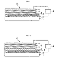
- FIGS 1 to 4 are schematic sectional views illustrating the layer structure of the organic electroluminescent devices according to aspects of the invention, and Figures 1, 2 , and 3 respectively show examples of the devices having plural organic compound layers, while Figure 4 shows an example of the device having one organic compound layer.
- the invention will be described hereinafter, as the same codes are allocated to the units having the same function in Figures 1 to 4 .
- the organic electroluminescent device 10 shown in Figure 1 has a transparent insulator substrate 1, and a transparent electrode 2, a buffer layer 3, a light-emitting layer 5, an electron-transporting layer 6 and a rear-face electrode 8 formed thereon successively. At least the light-emitting layer 5 has a charge transporting polyether.
- the organic electroluminescent device achieves both of the improved easiness in production and the luminescence efficiency in comparison with devices having other layer structures.
- the reason why the structure makes production easier and also improves luminescence efficiency in comparison with other layer structures is not known, it is thought to be due to the layer structure having fewer layers in comparison with other layer structures that divide all the functions into separate layers, and thereby, the injection efficiency of electrons, which generally have lower mobility than holes, is supplemented, thus balancing the charges in the light-emitting layer.
- the organic electroluminescent device 10 shown in Figure 2 has a transparent insulator substrate 1, and a transparent electrode 2, a buffer layer 3, a hole-transporting layer 4, a light-emitting layer 5, an electron-transporting layer 6 and a rear-face electrode 8 formed thereon successively. At least the hole-transporting layer 4 has a charge transporting polyether.
- the organic electroluminescent device achieves both of the improved luminescence efficiency and capability to drive at a lower voltage in comparison with devices having other layer structures.
- the reason why the structure achieves both of improved luminescence efficiency and improved driving capability at a lower voltage in comparison with other layer structures is not known, it is thought to be due to the separation of all the functions, which maximizes the injection efficiency in comparison with other layer structures, and the charges being recombinable in the light-emitting layer.
- the organic electroluminescent device 10 shown in Figure 3 has a transparent insulator substrate 1, and a transparent electrode 2, a buffer layer 3, a hole-transporting layer 4, a light-emitting layer 5 and a rear-face electrode 8 formed thereon in this order. At least the hole-transporting layer 4 has a charge transporting polyether.
- the organic electroluminescent device achieves both of the improved easiness in production and the durability in comparison with devices having other layer structures.
- the reason why the structure makes production easier and improves durability in comparison with other layer structures is not known, it is thought to be due to the layer structure having fewer layers in comparison with other layer structures that divide all the functions into separate layers, thereby improving the efficiency of the injection of holes into the light-emitting layer, and suppressing excessive injection of electrons in the light-emitting layer.
- the organic electroluminescent device 10 shown in Figure 4 has a transparent insulator substrate 1, and a transparent electrode 2, a buffer layer 3, a carrier-transporting light-emitting layer 7, and a rear-face electrode 8 formed thereon in this order. At least the carrier-transporting light-emitting layer 7 has a charge transporting polyether.
- the organic electroluminescent device achieves both of the improved easiness in production and upsizing in comparison with devices having other layer structures.
- the reason why the structure makes production and area enlargement easier in comparison with other layer structures is not known, it is thought to be due to the layer structure having fewer layers in comparison with other layer structures, thereby allowing manufacture by a wet application process or the like.
- the light-emitting layer 5 and the light-emitting layer 7 having a carrier-transporting property may have a charge transporting material (an electron hole transporting material other than the charge transporting polyether, and/or an electron transporting material).
- the organic electroluminescent device achieves the resistance to charge buildup to improve durability.
- the reason why the structure achieves the resistance to charge buildup thereby improving durability is not known, it is thought to be due to the charge transporting property being improved or imparted to the layer, thereby providing the layer with resistance to charge buildup.
- the thickness of the organic compound layer in contact with the buffer layer is preferably about 20 nm to about 100 nm.
- the layer having the charge-transporting polyether may function as a light-emitting layer 5 or an electron-transporting layer 6, depending on its structure, in the layer structure of the organic electroluminescent device 10 shown in Figure 1 ; as a hole-transporting layer 4 or an electron-transporting layer 6, in the layer structure of the organic electroluminescent device 10 shown in Figure 2 ; as a hole-transporting layer 4 or a light-emitting layer 5, in the layer structure of the organic electroluminescent device 10 shown in Figure 3 ; and as a light-emitting layer 7 having a carrier-transporting property in the layer structure of the organic electroluminescent device 10 shown in Figure 4 .
- the charge-transporting polyether functions preferably as a hole-transporting material.
- the transparent insulator substrate 1 shown in any one of Figures 1 to 4 is preferably transparent for light transmission, and examples thereof include, but are not limited to, glass, plastic film, and the like.
- the transparent electrode 2 is also preferably transparent for light transmission, similarly to the transparent insulator substrate, and has a large work function (ionization potential) for hole injection, and examples thereof include, but are not limited to, oxide layers such as of indium tin oxide (ITO), tin oxide (NESA), indium oxide, and zinc oxide, and metal films, such as of gold, platinum, and palladium, formed by vapor deposition or sputtering.
- ITO indium tin oxide
- NESA tin oxide
- indium oxide and zinc oxide
- metal films such as of gold, platinum, and palladium
- the electron-transporting layer 6 may be formed only with the charge-transporting polyether with an added function (electron-transporting property) according to applications, but may be formed together with an electron-transporting material other than the charge-transporting polyether in an amount in the range of 1 to 50 wt%, for example for further improvement in electrical characteristics for control of electron transfer efficiency.
- the electron-transporting materials include oxazole compounds, oxadiazole compounds, nitro-substituted fluorenone compounds, diphenoquinone compounds, thiopyranedioxide compounds, fluorenylidenemethane compounds and the like. Particularly preferable examples thereof include, but are not limited to, the following exemplary compounds (V-1) to (V-3): When the electron-transporting layer 6 is formed without use of the charge-transporting polyether, the electron-transporting layer 6 is formed with the electron-transporting material.
- the hole-transporting layer 4 may be formed only with a charge-transporting polyether with an added functional (hole-transporting property) according to applications.
- the hole-transporting layer 4 may be formed together with a hole-transporting material other than the charge-transporting polyether in an amount in the range of equal to or approximately 1 to equal to or approximately 50 wt%, in view of controlling the hole mobility.
- the hole-transporting materials include tetraphenylenediamine compounds, triphenylamine compounds, carbazole compounds, stilbene compounds, arylhydrazone compounds, porphyrin compounds, and the like.
- More preferable examples thereof include the following exemplary compounds (VI-1) to (VI-7), and tetraphenylenediamine compound are particularly preferable, because they are superior in compatibility with the charge-transporting polyether.
- the material may be used as mixed, for example, with another common resin.
- p is an integer, which is preferably in the range of equal to or approximately 10 to equal to or approximately 100,000, more preferably in the range of equal to or approximately 1,000 to equal to or approximately 50,000.
- the organic electroluminescent device 10 has a configuration of the organic electroluminescent device shown in Figure 1, 2 or 3
- a compound having a fluorescence quantum yield higher than that of other compounds in the solid state is used as the light-emitting material in the light-emitting layer 5.
- the light-emitting material is an organic low-molecular weight
- the compound should give a favorable thin film by vacuum deposition or by coating/drying of a solution or dispersion containing a low-molecular weight compound and a binder resin.
- it is a polymer, it should give a favorable thin film by coating/drying of a solution or dispersion containing it.
- the light-emitting material is an organic low-molecular weight compound
- preferable examples thereof include chelating organic metal complexes, polynuclear or fused aromatic ring compounds, perylene compounds, coumarin compounds, styryl arylene compounds, silole compounds, oxazole compounds, oxathiazole compounds, oxadiazole compounds, and the like.
- the light-emitting material is a polymer, examples thereof include poly-para-phenylene compounds, poly-para-phenylene vinylene compounds, polythiophene compounds, polyacetylene compounds, polyfluorene compounds and the like.
- Specifically preferable examples include, but are not limited to, the following exemplary compounds (VII-1) to (VII-17).
- each of Ar and X is a monovalent or divalent group having a structure similar to Ar and X shown in Formulae (II-1) and (II-2); each of n and x is an integer of 1 or more; and y is 0 or 1.
- a dye compound different from the light-emitting material may be doped as a guest material into the light-emitting material, for improvement in durability or luminous efficiency of the organic electroluminescent device 10. Doping is performed by vapor co-deposition when the light-emitting layer is formed by vacuum deposition, while by mixing to a solution or dispersion when the light-emitting layer is formed by coating/drying of the solution or dispersion.
- the degree of the dye compound doping in the light-emitting layer is approximately 0.001 to approximately 40 wt%, preferably approximately 0.01 to approximately 10 wt%.
- Examples of the dye compound used in doping include an organic compound having good compatibility with the light-emitting material and giving no prevention to form a favorable thin-film light-emitting layer, and favorable examples thereof include DCM compounds, quinacridone compounds, rubrene compounds, porphyrin compounds and the like. Specifically favorable examples thereof include, but are not limited to, the following compounds (VIII-1) to (VIII-4).
- the light-emitting layer 5 has the charge-transporting polyether in addition to the light-emitting material.
- the light-emitting layer 5 may be formed only with the light-emitting material, or alternatively, the light-emitting layer 5 may have the charge-transporting polyether in addition to the light-emitting material.
- the light-emitting layer 5 may further have a charge-transporting material which is different from the charge-transporting polyether.
- the charge-transporting polyether may be added to and dispersed in the light-emitting material in an amount in the range of about 1 to about 50 wt%, or alternatively, a charge-transporting material other than the charge-transporting polyether may be added to and dispersed in the light-emitting polymer in an amount in the range of about 1 to about 50 wt% before preparation of the light-emitting layer, in view of improving electrical properties and light-emitting characteristics.
- the light-emitting layer 7 having a carrier-transporting property is an organic compound layer which has the charge-transporting polyether and a light-emitting material (such as a material having any one of the light-emitting compounds (VII-1) to (VII-17)) in an amount of 50 wt% or less relative to the total amount of the layer and is dispersed in the charge-transporting polyether and is imparted with a function (hole- or electron-transporting property) in accordance with purposes.
- a charge-transporting material other than the charge-transporting polyether may be dispersed in an amount of 10 to 50 wt% relative to the total amount of the layer for control of the balance of hole and electron injected.
- the charge-transporting material for adjustment of electron transfer efficiency of the carrier-transporting light-emitting layer 7 include an oxadiazole compound, a nitro-substituted fluorenone compound, a diphenoquinone compound, a thiopyranedioxide compound, a fluorenylidenemethane compound and the like. More preferable examples thereof include the exemplary compounds (V-1) to (V-3).
- the charge-transporting material for use is preferably an organic compound having no strong electronic interaction with the charge-transporting polyether, and preferable examples thereof include the following compound (19).
- the hole-transporting material is preferably a tetraphenylenediamine compound, a triphenylamine compound, a carbazole compound, a stilbene compound, an aryl hydrazone compound, a porphyrin compound, or the like, and specifically favorable examples thereof include the exemplary compounds (VI-1) to (VI-7).
- tetraphenylenediamine compounds are preferable, because they are more compatible with the charge-transporting polyether.
- a metal element allowing vacuum deposition and having a small work function permitting electron injection is used for the rear-face electrode 8, and particularly favorable examples thereof include magnesium, aluminum, silver, indium, the alloys thereof, metal halogen compounds such as lithium fluoride or lithium oxide, metal oxides, and alkali metals such as lithium, calcium, barium, or cesium.
- a protective layer may be provided additionally on the rear-face electrode 8 for prevention of degradation of the device by water or oxygen.
- a material for the protective layer include metals such as In, Sn, Pb, Au, Cu, Ag, and A1; metal oxides such as MgO, SiO 2 , or TiO 2 ; and resins such as polyethylene resin, polyurea resin, or polyimide resin. Vacuum deposition, sputtering, plasma polymerization, CVD, or coating may be used in forming the protective layer.
- the organic electroluminescent device 10 shown in any one of Figures 1 to 4 can be prepared in the following manner: First, a buffer layer 3 is formed on a transparent electrode 2 previously formed on a transparent insulator substrate 1. The buffer layer 3 is formed to be a thin layer by applying the above-described components on the transparent electrode 2 by a vacuum evaporation method, a sputtering method, a CVD method or the like.
- a hole-transporting layer 4, a light-emitting layer 5, an electron-transporting layer 6, and/or a light-emitting layer 7 having a carrier-transporting property are formed on the buffer layer 3 according to the layer structure of each organic electroluminescent device 10.
- the hole-transporting layer 4, the light-emitting layer 5, the electron-transporting layer 6 and the light-emitting layer 7 having a carrier-transporting property can be formed by vacuum deposition of the material for each layer.
- the layer is formed for example by spin coating or dip coating, by using a coating solution obtained by dissolving materials for each layer in organic solvent.
- each layer is preferably formed by a casting method of using a coating solution, while the each layer may be formed by an inkjet method.
- the film thickness of the formed buffer layer to be formed is preferably in the range of from equal to or approximately 1 nm to equal to or approximately 100 nm, particularly in the range of from equal to or approximately 10 nm to equal to or approximately 15 nm.
- the thickness of the carrier-transporting light-emitting layer 7 is preferably in the range of from equal to or approximately 30 nm to equal to or approximately 200 nm.
- Each material (the charge-transporting polyether, light-emitting material, etc.) may be present in the state of molecular dispersion or particular dispersion.
- a solvent which is capable of dissolving respective materials to obtain a coating solution in the molecular dispersion state
- the dispersion solvent should be properly selected considering the dispersibility and solubility of respective materials in order to obtain a coating solution in the state having particulates being dispersed.
- Various means such as ball mill, sand mill, paint shaker, attriter, homogenizer, and ultrasonicator are usable in preparing particular dispersion.
- a rear-face electrode 8 is formed on the light-emitting layer 5, the electron-transporting layer 6 or the light-emitting layer 7 having a charge-transporting property by vacuum deposition or the like to give an organic electroluminescent device 10 shown in any one of Figure 1 to 4 .
- the display device of the exemplary embodiment has the organic electroluminescent device of the exemplary embodiment and a driving means for driving the organic electroluminescent device.
- the display device of the exemplary embodiment makes upsizing and producing of the display device easier while achieving high brightness, excellent stability and durability.
- Examples of the display device include those, as specifically shown in Figures 1 to 4 , having, as the driving means, a voltage-applying device 9 which is connected to the pair of the transparent electrode 2 and the rear-face electrode 8 of the organic electroluminescent device 10 and applies a DC voltage between the pair of electrodes.
- Examples of the method for driving the organic electroluminescent device 10 by using the voltage-applying device 9 include a method including applying, between the pair of electrodes, a DC voltage of about 4 to about 20 V at a current density of about 1 to about 200 mA/cm 2 so that the organic electroluminescent device 10 emits light.
- the organic electroluminescent device is off course applicable to any display devices having plural pixel units (organic electroluminescent devices) arranged in a matrix form.
- the electrode pairs may be formed in a matrix form.
- Any conventionally known technology such as a simple matrix driving method of using multiple line electrodes and row electrodes and driving the row electrodes collectively according to the image information for each line electrode while the line electrodes, or active matrix driving method of using pixel electrodes allocated to respective pixels are scanned, may be used as the method of driving the display device.
- Synthesis example 1 2.1 g of the compound (IX-1) is placed in a 50-ml three-necked, pear-shaped flask, and allowed to react under heating for 8 hours. Thereafter, the flask is cooled to room temperature, and the reactant is dissolved in 50 ml of monochlorobenzene under heating. Insolubles are filtered through a 0.5- ⁇ m PTFE filter, and the filtrate is added dropwise to 500 ml of methanol under stirring thereby precipitating a polymer. The polymer is filtered, thoroughly washed with methanol, and then dried to obtain 1.5 g of charge transporting polyether (X-1). The molecular weight distribution is measured by GPC (gel permeation chromatography), and is found to have a molecular weight of 5.82 ⁇ 10 5 (polystyrene standard), wherein Mw/Mn is 1.43.
- GPC gel permeation chromatography
- Synthesis example 2 2.5 g of the compound (IX-2) is placed in a 50-ml three-necked, pear-shaped flask, and allowed to react under heating for 8 hours. Thereafter, the flask is cooled to room temperature, and the reactant is dissolved in 50 ml of monochlorobenzene under heating. Insolubles are filtered through a 0.5- ⁇ m PTFE filter, and the filtrate is added dropwise to 500 ml of methanol under stirring thereby precipitating a polymer. The polymer is filtered, thoroughly washed with methanol, and then dried to obtain 1.3 g of charge transporting polyether (X-2). The molecular weight distribution is measured by GPC (gel permeation chromatography), and is found to have a molecular weight of 9.52 ⁇ 10 4 (polystyrene standard), wherein Mw/Mn is 1.38.
- GPC gel permeation chromatography
- Synthesis example 3 4.7 g of the compound (IX-3) is placed in a 50-ml three-necked, pear-shaped flask, and allowed to react under heating for 8 hours. Thereafter, the flask is cooled to room temperature, and the reactant is dissolved in 50 ml of monochlorobenzene under heating. Insolubles are filtered through a 0.5- ⁇ m PTFE filter, and the filtrate is added dropwise to 500 ml of methanol under stirring thereby precipitating a polymer. The polymer is filtered, thoroughly washed with methanol, and then dried to obtain 3.2 g of charge transporting polyether (X-3). The molecular weight distribution is measured by GPC (gel permeation chromatography), and is found to have a molecular weight of 9.66 ⁇ 10 5 (polystyrene standard), wherein Mw/Mn is 1.25.
- GPC gel permeation chromatography
- Synthesis example 4 3.2 g of the compound (IX-4) is placed in a 50-ml three-necked, pear-shaped flask, and allowed to react under heating for 8 hours. Thereafter, the flask is cooled to room temperature, and the reactant is dissolved in 50 ml of monochlorobenzene under heating. Insolubles are filtered through a 0.5- ⁇ m PTFE filter, and the filtrate is added dropwise to 500 ml of methanol under stirring thereby precipitating a polymer. The polymer is filtered, thoroughly washed with methanol, and then dried to obtain 1.1 g of charge transporting polyether (X-4). The molecular weight distribution is measured by GPC (gel permeation chromatography), and is found to have a molecular weight of 8.39 ⁇ 10 4 (polystyrene standard), wherein Mw/Mn is 1.45.
- GPC gel permeation chromatography
- an organic electroluminescent device is prepared in the following manner by using the charge-transporting polyether prepared as described above.
- Example 1 A 2mm wide strip-shaped glass substrate is etched to form an ITO electrode.
- the ITO electrode is washed and dried.
- molybdenum trioxide (MoO 3 ) is applied onto the ITO electrode as a buffer layer material by vacuum deposition to form a buffer layer having a thickness of 10 nm.
- a charge transporting polyether [exemplary compound (X-1)] as a charge transporting material and 0.5 parts by weight of the following exemplary compound (XI, polyfluorene compound, Mw ⁇ 1 ⁇ 10 5 ) as a light-emitting polymer are mixed so as to prepare a 10% by weight chlorobenzene solution of the mixture.
- the resultant is filtered through a 0.1- ⁇ m polytetrafluoroethylene (PTFE) filter.
- the thus obtained solution is applied onto the buffer layer by spin coating to form a light-emitting layer having a thickness of 80 nm and a charge transporting property.
- a Mg-Ag alloy is deposited thereon by vapor co-deposition, forming a rear-face electrode of 2 mm in width and 150 nm in thickness that crosses the ITO electrode.
- the effective area of the formed organic electroluminescent device is 0.04 cm 2 .
- Example 2 A 2mm wide strip-shaped glass substrate is etched to form an ITO electrode.
- the ITO electrode is washed and dried.
- molybdenum trioxide (MoO 3 ) is applied onto the ITO electrode as a buffer layer material by vacuum deposition to form a buffer layer having a thickness of 10 nm.
- a 5% by weight chlorobenzene solution of a charge transporting polyether [exemplary compound (X-2)] as an electron hole transporting material is prepared, filtered through a 0.1- ⁇ m polytetrafluoroethylene (PTFE) filter, and then applied onto the buffer layer by spin coating thereby forming an hole transporting layer having a thickness of 30 nm.
- a charge transporting polyether [exemplary compound (X-2)] as an electron hole transporting material
- sublimation purified Alq 3 (exemplary compound VII-1) as a luminescent material is placed in a tungsten boat, and evaporated by vacuum deposition to form a light-emitting layer having a thickness of 50 nm on the hole transporting layer.
- the degree of vacuum is 133.3 ⁇ 10 -3 Pa (1 ⁇ 10 -5 Torr), and the boat temperature is 300°C.
- a Mg-Ag alloy is deposited thereon by vapor co-deposition, forming a rear-face electrode of 2 mm in width and 150 nm in thickness that crosses the ITO electrode.
- the effective area of the formed organic electroluminescent device is 0.04 cm 2 .
- Example 3 A 2mm wide strip-shaped glass substrate is etched to form an ITO electrode.
- the ITO electrode is washed and dried.
- molybdenum trioxide (MoO 3 ) is applied onto the ITO electrode as a buffer layer material by vacuum deposition to form a buffer layer having a thickness of 10 nm.
- a 5% by weight chlorobenzene solution of a charge transporting polyether [exemplary compound (X-3)] as an electron hole transporting material is prepared, filtered through a 0.1- ⁇ m polytetrafluoroethylene (PTFE) filter, and then applied onto the buffer layer by spin coating thereby forming an hole transporting layer having a thickness of 30 nm.
- a charge transporting polyether [exemplary compound (X-3)] as an electron hole transporting material
- sublimation purified Alq 3 (exemplary compound VII-1) as a luminescent material is placed in a tungsten boat, and evaporated by vacuum deposition to form a light-emitting layer having a thickness of 50 nm on the hole transporting layer.
- the degree of vacuum is 133.3 ⁇ 10 -3 Pa (1 ⁇ 10 -5 Torr), and the boat temperature is 300°C.
- a Mg-Ag alloy is deposited thereon by vapor co-deposition, forming a rear-face electrode of 2 mm in width and 150 nm in thickness that crosses the ITO electrode.
- the effective area of the formed organic electroluminescent device is 0.04 cm 2 .
- Example 4 A 2mm wide strip-shaped glass substrate is etched to form an ITO electrode.
- the ITO electrode is washed and dried.
- molybdenum trioxide (MoO 3 ) is applied onto the ITO electrode as a buffer layer material by vacuum deposition to form a buffer layer having a thickness of 10 nm.
- a charge transporting polyether [exemplary compound (X-4)] as a charge transporting material and 0.1 parts by weight of the following exemplary compound (XII, PPV (poly(phenylene vinylene)) compound, Mw ⁇ 1 ⁇ 10 5 ) as a light-emitting polymer are mixed so as to prepare a 10% by weight chlorobenzene solution of the mixture.
- the resultant is filtered through a 0.1- ⁇ m polytetrafluoroethylene (PTFE) filter.
- the thus obtained solution is applied onto the buffer layer by spin coating to form a light-emitting layer having a thickness of 80 nm and a charge transporting property.
- a Mg-Ag alloy is deposited thereon by vapor co-deposition, forming a rear-face electrode of 2 mm in width and 150 nm in thickness that crosses the ITO electrode.
- the effective area of the formed organic electroluminescent device is 0.04 cm 2 .
- Example 5 An organic electroluminescent device is prepared in a similar manner to Example 1, except that vanadium troxide (VO 3 ) is used as the material for forming the buffer layer.
- VO 3 vanadium troxide
- Example 6 An organic electroluminescent device is prepared in a similar manner to Example 2, except that vanadium troxide (VO 3 ) is used as the material for forming the buffer layer.
- VO 3 vanadium troxide
- Example 7 An organic electroluminescent device is prepared in a similar manner to Example 3, except that vanadium troxide (VO 3 ) is used as the material for forming the buffer layer.
- VO 3 vanadium troxide
- Example 8 An organic electroluminescent device is prepared in a similar manner to Example 4, except that vanadium troxide (VO 3 ) is used as the material for forming the buffer layer.
- VO 3 vanadium troxide
- Comparative Example 1 An organic electroluminescent device is prepared in a similar manner to Example 1, except that a light-emitting layer is formed directly on the ITO electrode-sided surface of an ITO electrode-carrying glass plate without forming the buffer layer.
- Comparative Example 2 An organic electroluminescent device is prepared in a similar manner to Example 2, except that a light-emitting layer is formed directly on the ITO electrode-sided surface of an ITO electrode-carrying glass plate without forming the buffer layer.
- Comparative Example 3 An organic electroluminescent device is prepared in a similar manner to Example 3, except that a light-emitting layer is formed directly on the ITO electrode-sided surface of an ITO electrode-carrying glass plate without forming the buffer layer.
- Comparative Example 4 An organic electroluminescent device is prepared in a similar manner to Example 4, except that a light-emitting layer is formed directly on the ITO electrode-sided surface of an ITO electrode-carrying glass plate without forming the buffer layer.
- Comparative Example 5 An organic electroluminescent device is prepared in a similar manner to Example 3, except that a charge-transporting polymer having a vinyl skeleton [compound (XIII), Mw: 5.46 ⁇ 10 4 (polystyrene standard)] is used as a hole-transporting material in place of the charge-transporting polyether.
- Comparative Example 6 An organic electroluminescent device is prepared in a similar manner to Example 3, except that a charge-transporting polymer having a polycarbonate skeleton [compound (XIV), Mw: 7.83 ⁇ 10 4 (polystyrene standard)] is used as a hole-transporting material in place of the charge-transporting polyether.
- a charge-transporting polymer having a polycarbonate skeleton compound (XIV), Mw: 7.83 ⁇ 10 4 (polystyrene standard)
- Comparative Example 7 An organic electroluminescent device is prepared in a similar manner to Example 4, except that a charge-transporting polymer having a vinyl skeleton [compound (XIII), Mw: 5.46 ⁇ 10 4 (polystyrene standard)] is used as a hole-transporting material in place of the charge-transporting polyether.
- Comparative Example 8 An organic electroluminescent device is prepared in a similar manner to Example 4, except that a charge-transporting polymer having a polycarbonate skeleton [compound (XIV), Mw: 7.83 ⁇ 10 4 (polystyrene standard)] is used as a hole-transporting material in place of the charge-transporting polyether.
- a charge-transporting polymer having a polycarbonate skeleton compound (XIV), Mw: 7.83 ⁇ 10 4 (polystyrene standard)
- the organic electroluminescent devices shown in Examples 1 to 8 provide improved in charge-injecting efficiency and charge balance, as well as are superior stability, higher brightness and longer lifetime than the organic electroluminescent devices of Comparative examples 1 to 8.
Landscapes
- Chemical & Material Sciences (AREA)
- Engineering & Computer Science (AREA)
- Materials Engineering (AREA)
- Electroluminescent Light Sources (AREA)
Claims (14)
- Dispositif électroluminescent organique (10) comprenant une anode et une cathode formant une paire d'électrodes (2, 8), au moins une électrode (2) étant transparente ou translucide, et une couche tampon (3) et une couche de composé organique disposée entre l'anode et la cathode, caractérisé en ce que
la couche de composant organique (4) comprend une couche ou davantage avec au moins une couche émettrice de lumière (5) ;
au moins l'une des couches de la couche de composant organique est pourvue d'au moins un polyéther de transport de charge représenté par la Formule (I) :au moins l'une des couches est pourvue du polyéther de transport de charge situé en contact avec la couche tampon ; etla couche tampon située en contact avec l'anode est pourvue d'au moins un matériau d'injection de charge sélectionné parmi le groupe constitué d'un oxyde inorganique, d'un nitrure inorganique et d'un oxynitrure inorganique :dans la Formule (I), A représente au moins une structure représentée par la Formule (II-1) ou par la Formule (II-2) ; R représente un atome d'hydrogène, un groupe alkyle, un groupe aryle substitué ou non substitué, un groupe aralkyle substitué ou non substitué, un groupe acyle ou un groupe représenté par -CONH-R' (dans lequel R' représente un atome d'hydrogène, un groupe alkyle, un groupe aryle substitué ou non substitué ou un groupe aralkyle substitué ou non substitué) ; et p est un nombre entier de 5 à 5000,

- Dispositif électroluminescent organique de la revendication 1, dans lequel la couche tampon est pourvue d'au moins l'un d'un oxyde de molybdène et d'un oxyde de vanadium.
- Dispositif électroluminescent organique de la revendication 1, dans lequel Ar dans les formules (II-1) et (II-2) représente un groupe aromatique monovalent sélectionné parmi le groupe constitué d'un groupe benzène substitué ou non substitué, d'un groupe biphényle monovalent substitué ou non substitué, d'un groupe naphtalène monovalent substitué ou non substitué et d'un groupe fluorène monovalent substitué ou non substitué.
- Dispositif électroluminescent organique de la revendication 1, dans lequel T dans les Formules (II-1) et (II-2) représente -CH2-, -(CH2)2-, -(CH2)3, ou -(CH2)4-,
- Dispositif électroluminescent organique de la revendication 1, dans lequel l'épaisseur de la couche tampon se situe dans la plage de 1nm à environ 15 nm.
- Dispositif électroluminescent organique de la revendication 1, dans lequel la couche de composé organique est pourvue de la couche émettrice de lumière et d'une couche de transport d'électrons, au moins la couche émettrice de lumière est pourvue d'au moins un polyéther de transport de charge représenté par la Formule (I) et la couche tampon est disposée entre l'anode et la couche émettrice de lumière.
- Dispositif électroluminescent de la revendication 6, dans lequel la couche émettrice de lumière contient en outre un matériau de transport de charge autre que le polyéther de transport de charge.
- Dispositif électroluminescent organique de la revendication 1, dans lequel la couche de composé organique est pourvue d'une couche de transport de trous, de la couche émettrice de lumière et d'une couche de transport d'électrons, au moins la couche de transport d'électrons est pourvue d'au moins un polyéther de transport de charge représenté par la Formule (I) et la couche tampon est disposée entre l'anode et la couche de transport de trous.
- Dispositif électroluminescent organique de la revendication 8, dans lequel la couche émettrice de lumière est pourvue d'un matériau de transport de charge autre que le polyéther de transport de charge.
- Dispositif électroluminescent organique de la revendication 1, dans lequel la couche de composé organique est pourvue d'une couche de transport de trous et de la couche émettrice de lumière, au moins la couche de transport de trous est pourvue d'au moins un polyéther de transport de charge représenté par la Formule (I) et la couche tampon est disposée entre l'anode et la couche de transport de trous.
- Dispositif électroluminescent organique de la revendication 10, dans lequel la couche émettrice de lumière est en outre pourvue d'un matériau de transport de charge autre que le polyéther de transport de charge.
- Dispositif électroluminescent organique de la revendication 1, dans lequel la couche de composé organique consiste d'une couche émettrice de lumière, la couche émettrice de lumière ayant une propriété de transport de charge, la couche émettrice de lumière étant pourvue d'au moins un polyéther de transport de charge représenté par la Formule (I) et la couche tampon étant disposée entre l'anode et la couche émettrice de lumière.
- Dispositif électroluminescent organique de la revendication 12, dans lequel la couche émettrice de lumière est pourvue d'un matériau de transport de charge autre que le polyéther de transport de charge.
- Dispositif d'affichage comprenant :un substrat ;une pluralité de dispositifs électroluminescents organiques disposés sur le substrat et agencés sous forme de matrice ; etune unité de commande qui commande les dispositifs électroluminescents organiques, chacun des dispositifs électroluminescents organiques étant le dispositif électroluminescent organique de l'une quelconque des revendications 1 à 13.
Applications Claiming Priority (1)
| Application Number | Priority Date | Filing Date | Title |
|---|---|---|---|
| JP2007096670A JP2008258272A (ja) | 2007-04-02 | 2007-04-02 | 有機電界発光素子及び表示装置 |
Publications (3)
| Publication Number | Publication Date |
|---|---|
| EP1978571A2 EP1978571A2 (fr) | 2008-10-08 |
| EP1978571A3 EP1978571A3 (fr) | 2011-03-23 |
| EP1978571B1 true EP1978571B1 (fr) | 2012-04-25 |
Family
ID=39591156
Family Applications (1)
| Application Number | Title | Priority Date | Filing Date |
|---|---|---|---|
| EP08102434A Expired - Fee Related EP1978571B1 (fr) | 2007-04-02 | 2008-03-10 | Dispositif électroluminescent organique et dispositif d'affichage |
Country Status (5)
| Country | Link |
|---|---|
| US (1) | US20080238832A1 (fr) |
| EP (1) | EP1978571B1 (fr) |
| JP (1) | JP2008258272A (fr) |
| KR (1) | KR20080090271A (fr) |
| CN (1) | CN101282604B (fr) |
Families Citing this family (2)
| Publication number | Priority date | Publication date | Assignee | Title |
|---|---|---|---|---|
| KR101191645B1 (ko) | 2009-11-25 | 2012-10-17 | 삼성디스플레이 주식회사 | 유기 발광 표시 장치 및 그 제조 방법 |
| CN102709310B (zh) * | 2012-06-11 | 2016-04-20 | 无锡格菲电子薄膜科技有限公司 | 一种柔性有机发光晶体管显示器件 |
Family Cites Families (10)
| Publication number | Priority date | Publication date | Assignee | Title |
|---|---|---|---|---|
| JP2894257B2 (ja) | 1994-10-24 | 1999-05-24 | 富士ゼロックス株式会社 | 新規電荷輸送性ポリマー、その製造法およびそれを用いた有機電子デバイス |
| JP3528370B2 (ja) | 1995-02-03 | 2004-05-17 | 富士ゼロックス株式会社 | 有機電界発光素子 |
| JPH10321376A (ja) * | 1997-03-19 | 1998-12-04 | Minolta Co Ltd | 有機エレクトロルミネセンス素子 |
| CN1213127C (zh) * | 1998-09-09 | 2005-08-03 | 出光兴产株式会社 | 有机电致发光器件与苯二胺衍生物 |
| JP2002075654A (ja) * | 2000-08-28 | 2002-03-15 | Fuji Xerox Co Ltd | 有機電界発光素子 |
| US7015882B2 (en) * | 2000-11-07 | 2006-03-21 | Sony Corporation | Active matrix display and active matrix organic electroluminescence display |
| JP3895938B2 (ja) * | 2001-03-22 | 2007-03-22 | 三洋電機株式会社 | 有機エレクトロルミネッセンス素子およびその製造方法 |
| EP1722602A1 (fr) * | 2004-03-05 | 2006-11-15 | Idemitsu Kosan Co., Ltd. | Dispositif electroluminescent organique et affichage electroluminescent organique |
| US20060046094A1 (en) * | 2004-09-01 | 2006-03-02 | Fuji Xerox Co., Ltd. | Organic electroluminescence device |
| CN1888008A (zh) * | 2006-02-10 | 2007-01-03 | 淮海工学院 | 可发射蓝光聚合物材料及其制备方法 |
-
2007
- 2007-04-02 JP JP2007096670A patent/JP2008258272A/ja not_active Withdrawn
-
2008
- 2008-03-05 KR KR1020080020412A patent/KR20080090271A/ko not_active Ceased
- 2008-03-06 US US12/043,756 patent/US20080238832A1/en not_active Abandoned
- 2008-03-07 CN CN2008100829211A patent/CN101282604B/zh not_active Expired - Fee Related
- 2008-03-10 EP EP08102434A patent/EP1978571B1/fr not_active Expired - Fee Related
Also Published As
| Publication number | Publication date |
|---|---|
| US20080238832A1 (en) | 2008-10-02 |
| KR20080090271A (ko) | 2008-10-08 |
| CN101282604A (zh) | 2008-10-08 |
| EP1978571A3 (fr) | 2011-03-23 |
| CN101282604B (zh) | 2010-10-13 |
| JP2008258272A (ja) | 2008-10-23 |
| EP1978571A2 (fr) | 2008-10-08 |
Similar Documents
| Publication | Publication Date | Title |
|---|---|---|
| US6670052B2 (en) | Organic light emitting diode | |
| EP2019440A2 (fr) | Dispositif électroluminescent organique et dispositif d'affichage | |
| JP4269613B2 (ja) | 有機電界発光素子 | |
| JP2004087395A (ja) | 有機電界発光素子 | |
| US7183009B2 (en) | Organic electroluminescent element | |
| KR100858458B1 (ko) | 유기 전계발광소자 | |
| EP1978571B1 (fr) | Dispositif électroluminescent organique et dispositif d'affichage | |
| US8435646B2 (en) | Organic electroluminescent device and display device | |
| JP4265184B2 (ja) | 有機電界発光素子 | |
| JP4254170B2 (ja) | 有機電界発光素子 | |
| JP4518167B2 (ja) | 有機電界発光素子及び表示媒体 | |
| JP2005158561A (ja) | 有機電界発光素子 | |
| JP4078921B2 (ja) | 有機電界発光素子 | |
| JP4321012B2 (ja) | 有機電界発光素子 | |
| JP4254169B2 (ja) | 有機電界発光素子 | |
| JP4122722B2 (ja) | 有機電界発光素子 | |
| JP2008305996A (ja) | 有機電界発光素子及び表示装置 | |
| JP3855640B2 (ja) | 有機電界発光素子 | |
| JP2008305995A (ja) | 有機電界発光素子及び表示装置 | |
| JP4258192B2 (ja) | 有機電界発光素子 | |
| JP2008160023A (ja) | 有機電界発光素子及び表示装置 | |
| JP2007180072A (ja) | 有機電界発光素子 | |
| JP2008016504A (ja) | 有機電界発光素子 | |
| JP2007317966A (ja) | 有機電界発光素子およびその製造方法、並びに画像表示媒体 | |
| JP2007123432A (ja) | 有機電界発光素子 |
Legal Events
| Date | Code | Title | Description |
|---|---|---|---|
| PUAI | Public reference made under article 153(3) epc to a published international application that has entered the european phase |
Free format text: ORIGINAL CODE: 0009012 |
|
| 17P | Request for examination filed |
Effective date: 20080312 |
|
| AK | Designated contracting states |
Kind code of ref document: A2 Designated state(s): AT BE BG CH CY CZ DE DK EE ES FI FR GB GR HR HU IE IS IT LI LT LU LV MC MT NL NO PL PT RO SE SI SK TR |
|
| AX | Request for extension of the european patent |
Extension state: AL BA MK RS |
|
| PUAL | Search report despatched |
Free format text: ORIGINAL CODE: 0009013 |
|
| AK | Designated contracting states |
Kind code of ref document: A3 Designated state(s): AT BE BG CH CY CZ DE DK EE ES FI FR GB GR HR HU IE IS IT LI LT LU LV MC MT NL NO PL PT RO SE SI SK TR |
|
| AX | Request for extension of the european patent |
Extension state: AL BA MK RS |
|
| GRAJ | Information related to disapproval of communication of intention to grant by the applicant or resumption of examination proceedings by the epo deleted |
Free format text: ORIGINAL CODE: EPIDOSDIGR1 |
|
| GRAP | Despatch of communication of intention to grant a patent |
Free format text: ORIGINAL CODE: EPIDOSNIGR1 |
|
| RIC1 | Information provided on ipc code assigned before grant |
Ipc: H01L 51/54 20060101ALI20110920BHEP Ipc: H01L 51/50 20060101ALI20110920BHEP Ipc: H01L 51/00 20060101AFI20110920BHEP |
|
| AKX | Designation fees paid |
Designated state(s): DE GB NL |
|
| GRAS | Grant fee paid |
Free format text: ORIGINAL CODE: EPIDOSNIGR3 |
|
| GRAA | (expected) grant |
Free format text: ORIGINAL CODE: 0009210 |
|
| AK | Designated contracting states |
Kind code of ref document: B1 Designated state(s): DE GB NL |
|
| REG | Reference to a national code |
Ref country code: GB Ref legal event code: FG4D |
|
| REG | Reference to a national code |
Ref country code: DE Ref legal event code: R096 Ref document number: 602008015125 Country of ref document: DE Effective date: 20120621 |
|
| REG | Reference to a national code |
Ref country code: NL Ref legal event code: T3 |
|
| PLBE | No opposition filed within time limit |
Free format text: ORIGINAL CODE: 0009261 |
|
| STAA | Information on the status of an ep patent application or granted ep patent |
Free format text: STATUS: NO OPPOSITION FILED WITHIN TIME LIMIT |
|
| 26N | No opposition filed |
Effective date: 20130128 |
|
| PGFP | Annual fee paid to national office [announced via postgrant information from national office to epo] |
Ref country code: DE Payment date: 20130306 Year of fee payment: 6 Ref country code: GB Payment date: 20130306 Year of fee payment: 6 |
|
| REG | Reference to a national code |
Ref country code: DE Ref legal event code: R097 Ref document number: 602008015125 Country of ref document: DE Effective date: 20130128 |
|
| PGFP | Annual fee paid to national office [announced via postgrant information from national office to epo] |
Ref country code: NL Payment date: 20130316 Year of fee payment: 6 |
|
| REG | Reference to a national code |
Ref country code: DE Ref legal event code: R119 Ref document number: 602008015125 Country of ref document: DE |
|
| REG | Reference to a national code |
Ref country code: NL Ref legal event code: V1 Effective date: 20141001 |
|
| GBPC | Gb: european patent ceased through non-payment of renewal fee |
Effective date: 20140310 |
|
| REG | Reference to a national code |
Ref country code: DE Ref legal event code: R119 Ref document number: 602008015125 Country of ref document: DE Effective date: 20141001 |
|
| PG25 | Lapsed in a contracting state [announced via postgrant information from national office to epo] |
Ref country code: DE Free format text: LAPSE BECAUSE OF NON-PAYMENT OF DUE FEES Effective date: 20141001 Ref country code: GB Free format text: LAPSE BECAUSE OF NON-PAYMENT OF DUE FEES Effective date: 20140310 |
|
| PG25 | Lapsed in a contracting state [announced via postgrant information from national office to epo] |
Ref country code: NL Free format text: LAPSE BECAUSE OF NON-PAYMENT OF DUE FEES Effective date: 20141001 |