EP1964100B1 - Apparatus and method for color shift compensation in displays - Google Patents
Apparatus and method for color shift compensation in displays Download PDFInfo
- Publication number
- EP1964100B1 EP1964100B1 EP06832166A EP06832166A EP1964100B1 EP 1964100 B1 EP1964100 B1 EP 1964100B1 EP 06832166 A EP06832166 A EP 06832166A EP 06832166 A EP06832166 A EP 06832166A EP 1964100 B1 EP1964100 B1 EP 1964100B1
- Authority
- EP
- European Patent Office
- Prior art keywords
- sub
- pixels
- pixel
- row
- frame
- Prior art date
- Legal status (The legal status is an assumption and is not a legal conclusion. Google has not performed a legal analysis and makes no representation as to the accuracy of the status listed.)
- Not-in-force
Links
- 238000000034 method Methods 0.000 title claims description 15
- 239000011159 matrix material Substances 0.000 claims abstract description 21
- 239000003990 capacitor Substances 0.000 claims description 6
- 229910021420 polycrystalline silicon Inorganic materials 0.000 claims description 4
- 229920005591 polysilicon Polymers 0.000 claims description 4
- 238000007496 glass forming Methods 0.000 claims 1
- 239000011521 glass Substances 0.000 description 8
- 230000003071 parasitic effect Effects 0.000 description 4
- 230000006866 deterioration Effects 0.000 description 3
- 239000004973 liquid crystal related substance Substances 0.000 description 3
- 238000012935 Averaging Methods 0.000 description 2
- 230000002238 attenuated effect Effects 0.000 description 2
- 238000005516 engineering process Methods 0.000 description 2
- 238000010420 art technique Methods 0.000 description 1
- 239000003086 colorant Substances 0.000 description 1
- 230000001419 dependent effect Effects 0.000 description 1
- 230000000694 effects Effects 0.000 description 1
- 230000010354 integration Effects 0.000 description 1
- 230000000704 physical effect Effects 0.000 description 1
- 229920001690 polydopamine Polymers 0.000 description 1
Images


Classifications
-
- G—PHYSICS
- G09—EDUCATION; CRYPTOGRAPHY; DISPLAY; ADVERTISING; SEALS
- G09G—ARRANGEMENTS OR CIRCUITS FOR CONTROL OF INDICATING DEVICES USING STATIC MEANS TO PRESENT VARIABLE INFORMATION
- G09G3/00—Control arrangements or circuits, of interest only in connection with visual indicators other than cathode-ray tubes
- G09G3/20—Control arrangements or circuits, of interest only in connection with visual indicators other than cathode-ray tubes for presentation of an assembly of a number of characters, e.g. a page, by composing the assembly by combination of individual elements arranged in a matrix no fixed position being assigned to or needed to be assigned to the individual characters or partial characters
- G09G3/34—Control arrangements or circuits, of interest only in connection with visual indicators other than cathode-ray tubes for presentation of an assembly of a number of characters, e.g. a page, by composing the assembly by combination of individual elements arranged in a matrix no fixed position being assigned to or needed to be assigned to the individual characters or partial characters by control of light from an independent source
- G09G3/36—Control arrangements or circuits, of interest only in connection with visual indicators other than cathode-ray tubes for presentation of an assembly of a number of characters, e.g. a page, by composing the assembly by combination of individual elements arranged in a matrix no fixed position being assigned to or needed to be assigned to the individual characters or partial characters by control of light from an independent source using liquid crystals
- G09G3/3611—Control of matrices with row and column drivers
- G09G3/3685—Details of drivers for data electrodes
- G09G3/3688—Details of drivers for data electrodes suitable for active matrices only
-
- G—PHYSICS
- G09—EDUCATION; CRYPTOGRAPHY; DISPLAY; ADVERTISING; SEALS
- G09G—ARRANGEMENTS OR CIRCUITS FOR CONTROL OF INDICATING DEVICES USING STATIC MEANS TO PRESENT VARIABLE INFORMATION
- G09G2310/00—Command of the display device
- G09G2310/02—Addressing, scanning or driving the display screen or processing steps related thereto
- G09G2310/0264—Details of driving circuits
- G09G2310/0297—Special arrangements with multiplexing or demultiplexing of display data in the drivers for data electrodes, in a pre-processing circuitry delivering display data to said drivers or in the matrix panel, e.g. multiplexing plural data signals to one D/A converter or demultiplexing the D/A converter output to multiple columns
-
- G—PHYSICS
- G09—EDUCATION; CRYPTOGRAPHY; DISPLAY; ADVERTISING; SEALS
- G09G—ARRANGEMENTS OR CIRCUITS FOR CONTROL OF INDICATING DEVICES USING STATIC MEANS TO PRESENT VARIABLE INFORMATION
- G09G2320/00—Control of display operating conditions
- G09G2320/02—Improving the quality of display appearance
- G09G2320/0209—Crosstalk reduction, i.e. to reduce direct or indirect influences of signals directed to a certain pixel of the displayed image on other pixels of said image, inclusive of influences affecting pixels in different frames or fields or sub-images which constitute a same image, e.g. left and right images of a stereoscopic display
-
- G—PHYSICS
- G09—EDUCATION; CRYPTOGRAPHY; DISPLAY; ADVERTISING; SEALS
- G09G—ARRANGEMENTS OR CIRCUITS FOR CONTROL OF INDICATING DEVICES USING STATIC MEANS TO PRESENT VARIABLE INFORMATION
- G09G2320/00—Control of display operating conditions
- G09G2320/02—Improving the quality of display appearance
- G09G2320/0242—Compensation of deficiencies in the appearance of colours
Definitions
- the invention concerns active matrix display modules and methods for the color shift compensation implemented in active matrix display modules.
- the driving circuit for an active matrix LCD can be divided in two parts: a source and a gate driver.
- the gate driver controls the gates of the on glass transistors to select and deselect all pixels of a specific row.
- Each pixel consists of three sub-pixels (red, green, blue) and each sub-pixel has its own storage capacitor.
- the source drivers provide the required voltage level to all sub-pixels of the currently selected row corresponding to the desired intensity for each color. The final color is obtained by the ability of the human eye to mix combinations of the three base colors (red, green, blue) into one.
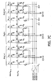
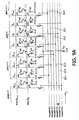
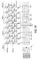
- Fig. 1 an example of an active matrix LTPS (low temperature polysilicon) display module 10 is schematically depicted.
- the gate driver circuit 12 is integrated directly into the display glass 11. This is possible since the gate driver 12 typically only comprises circuits that can easily be implemented on the display glass 11. Note that in theory, the gate driver could reside in a separate chip as well.
- the source drivers can either be integrated on-glass or in a separate chip.
- Fig. 1 an embodiment is shown where the demultiplexers 13 are integrated on the display glass 11.
- the multiplexers 14, source output drivers 15, latches 16, buffer 17 and control circuit 18 are realized in a separate source driver chip 20.
- the display panel has in the present example N columns and M rows.
- LTPS is an example only. The invention which will be addressed later is not LTPS specific.
- the on-glass demultiplexing method reduces the amount of source output pads needed to drive a specific display size. Or, in other words, it increases the possible display size that can be driven by a single chip.
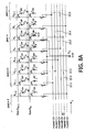
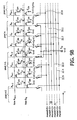
- the source lines are grouped, e.g. 3 sub-pixels per multiplexing group for a mux rate of 1:3 or 6 sub-pixels per multiplexing group for a mux rate of 1:6. When a row is selected, the sub-pixels therein are not charged all at the same time but the source lines of one group are charged sequentially.
- a multiplexing 1:3 case first all red sub-pixels are selected, then all green sub-pixels, and finally all blue sub-pixels. After that, the row is deselected, and the next row becomes selected, followed again by charging the red sub-pixels, and so on.
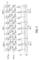
- Fig. 2 In this Figure two rows RN +1 and R N and three columns n-1, n, n+1 are illustrated. Each pixel has, as mentioned above, three sub-pixels.
- the sub-pixels of column n-1 are denoted as (red) R n-1 ), (green) G n-1 , and (blue) B n-1.
- the source driver lines 19 are denoted as S n-1 , S n , and S n+1 .
- the switches of the demultiplexer 13 carry the reference number 21 and the demultiplexer selection lines carry the reference number 22.
- C p are the parasitic capacitances between two adjacent source lines and C pix are the pixel capacitances.
- each sub-pixel comprises a sub-pixel selection transistor arranged at an intersection of a row and a column. One such sub-pixel selection transistor carries the reference number 23.
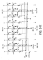
- the drawback of the demultiplexing method is the so-called color shift.
- all the on-glass sub-pixel selection transistors 23 for this row are conducting.
- charging a sub-pixel influences the neighboring pixels (which were charged before) through the parasitic capacitances C p between two lines (mainly the adjacent lines).
- the demultiplexer selection signals are shown on the left hand side right next to the demultiplexer selection lines 22.
- the color shift is denoted by ⁇ B & ⁇ G. Therefore, only the sub-pixels which were charged as the last ones in a row, carry the correct voltage level when the row becomes deselected (the blue sub-pixel in case of Fig. 3 ).
- the state of the art technique to compensate the color shift effect is to rotate the pixel order selection from frame to frame. In this way, the last charged pixels (those with the correct color) of a specific row are in each frame different. The color of the last selected sub-pixel is then correct and the error on each sub-pixel partially averages out over 3 frames for a mux-rate of 1:3 (or 6 frames for mux-rate 1:6, respectively). Depending on the frame frequency and on the multiplexing factor the amount of required frames to average out the errors might become too long and will be perceived as flicker on the display. Especially for high multiplexing rates, a high frame frequency must be applied to avoid flickering.
- US 2005/140633 discloses a common inversion LCD in which a sequence of digital video signals is changed over two frames in order to suppress colour errors.
- US 2005/035934 discloses a display drive scheme in which a two dimensional polarity inversion pattern is used to eliminate dc offset.
- US 2001/0050665 discloses a method of driving an LCD in which a data sequence is changed so that a uniform leakage current and uniform data signal change frequency can be obtained.
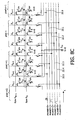
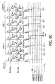
- the color shift is compensated using a smart selection order for the sub-pixels.
- the compensation takes place within two frames. During the first frame the color shift is partially compensated and during the second frame, the color shift is completely compensated.
- an active matrix display module comprises a driving circuit with a source driver and a gate driver. Furthermore, a display panel with pixels consisting of three sub-pixels is provided. The sub-pixels are arranged in rows and columns and each sub-pixel comprises a sub-pixel selection transistor arranged at an intersection of a row and a column.
- the gate driver is employed to select and deselect all pixels of a row of the display panel and the source driver is employed for providing the required voltage levels to all sub-pixels of a currently selected row, said voltage levels corresponding to the desired intensity for each color.
- Demultiplexer switches are integrated onto the display panel for demultiplexing rows of the display panel.
- the active matrix display module further comprises means for color shift compensation. These means implement a selection order for the selection of the sub-pixels to compensate unintentional color shifts. The compensation takes place within two frames.
- the color shift is compensated by a smart selection order employed when selecting the sub-pixels. This is done within two frames.
- the color shift is partially compensated, and in the second frame completely. In this way, flicker (which might be present in the prior art solution) is avoided.
- the inventive selection order proposed herein is also chosen to minimize power consumption.
- the display panel 11 comprises pixels consisting of three sub-pixels (R n , G n , B n ).
- the sub-pixels are arranged in rows where the row line (horizontal) is called gate line.
- Each sub-pixel comprises a sub-pixel selection transistor 23 arranged at an intersection of a row and a column.
- the sub-pixel selection transistors 23 in a row are all connected to individual, i.e. different, data lines (vertical/column lines).
- a gate driver 12 is employed to select and deselect all pixels of a row of the display panel 11.
- a source driver 20 provides the required voltage levels to all sub-pixels of a currently selected row of said display panel 11, said voltage levels corresponding to the desired intensity for each color.
- the corresponding demultiplexer switches may be integrated onto the display panel 11 for demultiplexing the data lines of the display panel 11.
- one demultiplexer switch is denoted as 21.1.
- the control circuit 18 may comprise a demultiplexer logic or a sequencer to control the demultiplexer switches 21 in accordance with the present invention. That is, the control circuit 18 provides the right signals in order to switch the demultiplexer switches 21 so that the above-identified properties are satisfied.
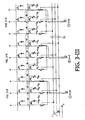
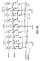
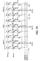
- a first embodiment of the invention is designed for a multiplexing rate (mux rate) of 1:3.
- multiplex rate 1:3.
- the above-mentioned properties 1, 2, and 3 are being used. It is to be noted that according to the invention other selection orders than described here are possible too.
- step 8 (carried out during the 3 rd and 4 th frame) is optional.
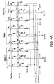
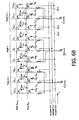
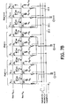
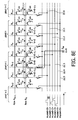
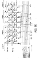
- a second embodiment of the invention is designed for a multiplexing rate (mux rate) of 1:6.
- the above-mentioned properties 1, 3, and 4 are being used. It is to be noted that according to the invention other selection orders than described here are possible too.
- each sub-pixel may be averaged out to 0V. This is realized in four frames. However, the color shift is partially compensated in each frame and completely over two frames, i.e. over frame 1 to frame 2 and over frame 3 to frame 4, respectively.
- the selection order for the selection of the sub-pixels is typically implemented inside the control circuit 18.
- This control circuit 18 provides the appropriate selection signals taking into account two or more of the properties 1 through 4 identified above.
- the present invention is intended to be used in LCD drivers where the source lines are multiplexed: Very well suited is the present invention for small displays, such as the ones used in mobile phones, PDAs, and the like.
Landscapes
- Engineering & Computer Science (AREA)
- Chemical & Material Sciences (AREA)
- Crystallography & Structural Chemistry (AREA)
- Physics & Mathematics (AREA)
- Computer Hardware Design (AREA)
- General Physics & Mathematics (AREA)
- Theoretical Computer Science (AREA)
- Liquid Crystal Display Device Control (AREA)
- Control Of Indicators Other Than Cathode Ray Tubes (AREA)
- Liquid Crystal (AREA)
- Packages (AREA)
- Investigating Or Analyzing Non-Biological Materials By The Use Of Chemical Means (AREA)
Priority Applications (1)
| Application Number | Priority Date | Filing Date | Title |
|---|---|---|---|
| EP06832166A EP1964100B1 (en) | 2005-12-16 | 2006-12-08 | Apparatus and method for color shift compensation in displays |
Applications Claiming Priority (3)
| Application Number | Priority Date | Filing Date | Title |
|---|---|---|---|
| EP05112275 | 2005-12-16 | ||
| EP06832166A EP1964100B1 (en) | 2005-12-16 | 2006-12-08 | Apparatus and method for color shift compensation in displays |
| PCT/IB2006/054693 WO2007069159A2 (en) | 2005-12-16 | 2006-12-08 | Apparatus and method for color shift compensation in displays |
Publications (2)
| Publication Number | Publication Date |
|---|---|
| EP1964100A2 EP1964100A2 (en) | 2008-09-03 |
| EP1964100B1 true EP1964100B1 (en) | 2011-04-20 |
Family
ID=38042576
Family Applications (1)
| Application Number | Title | Priority Date | Filing Date |
|---|---|---|---|
| EP06832166A Not-in-force EP1964100B1 (en) | 2005-12-16 | 2006-12-08 | Apparatus and method for color shift compensation in displays |
Country Status (7)
Families Citing this family (17)
| Publication number | Priority date | Publication date | Assignee | Title |
|---|---|---|---|---|
| US7839414B2 (en) * | 2007-07-30 | 2010-11-23 | Motorola Mobility, Inc. | Methods and devices for display color compensation |
| KR101117736B1 (ko) * | 2010-02-05 | 2012-02-27 | 삼성모바일디스플레이주식회사 | 디스플레이 장치 |
| TWI497477B (zh) * | 2010-05-13 | 2015-08-21 | Novatek Microelectronics Corp | 驅動模組與驅動方法 |
| CN102376281A (zh) * | 2010-08-23 | 2012-03-14 | 联咏科技股份有限公司 | 驱动模块与驱动方法 |
| WO2012102229A1 (ja) * | 2011-01-24 | 2012-08-02 | シャープ株式会社 | 表示装置およびその駆動方法 |
| KR101829777B1 (ko) * | 2011-03-09 | 2018-02-20 | 삼성디스플레이 주식회사 | 광 감지 센서 |
| US9147372B2 (en) * | 2011-03-31 | 2015-09-29 | Sharp Kabushiki Kaisha | Display device |
| US10311773B2 (en) * | 2013-07-26 | 2019-06-04 | Darwin Hu | Circuitry for increasing perceived display resolutions from an input image |
| CN103927978A (zh) * | 2013-12-31 | 2014-07-16 | 厦门天马微电子有限公司 | Amoled显示面板及有机发光显示装置 |
| CN104505038B (zh) * | 2014-12-24 | 2017-07-07 | 深圳市华星光电技术有限公司 | 一种液晶面板的驱动电路及液晶显示装置 |
| CN105096867B (zh) * | 2015-08-07 | 2018-04-10 | 深圳市华星光电技术有限公司 | 一种液晶显示器及其控制方法 |
| KR102509164B1 (ko) * | 2016-09-29 | 2023-03-13 | 엘지디스플레이 주식회사 | 표시장치 및 그를 이용한 서브픽셀 트랜지션 방법 |
| CN206194295U (zh) * | 2016-11-15 | 2017-05-24 | 京东方科技集团股份有限公司 | 数据线多路分配器、显示基板、显示面板及显示装置 |
| US10825410B2 (en) * | 2016-12-01 | 2020-11-03 | Lrx Investissement | Addressing mode and principle for constructing matrix screens for displaying colour images with quasi-static behavour |
| US10726796B2 (en) * | 2018-05-30 | 2020-07-28 | Wuhan China Star Optoelectronics Technology Co., Ltd. | Backlight drive circuit, driving method thereof, and display device |
| CN110111755A (zh) * | 2019-06-18 | 2019-08-09 | 厦门天马微电子有限公司 | 一种显示面板、其驱动方法及显示装置 |
| CN116092405B (zh) * | 2022-12-12 | 2024-06-14 | 北京视延科技有限公司 | 显示面板、显示驱动方法、显示驱动模组和显示装置 |
Family Cites Families (9)
| Publication number | Priority date | Publication date | Assignee | Title |
|---|---|---|---|---|
| JP4664466B2 (ja) | 2000-05-15 | 2011-04-06 | 東芝モバイルディスプレイ株式会社 | 表示装置 |
| KR100367010B1 (ko) * | 2000-06-08 | 2003-01-09 | 엘지.필립스 엘시디 주식회사 | 액정표시장치 및 그 구동방법 |
| KR100675320B1 (ko) * | 2000-12-29 | 2007-01-26 | 엘지.필립스 엘시디 주식회사 | 액정표시장치의 구동방법 |
| US6956553B2 (en) * | 2001-04-27 | 2005-10-18 | Sanyo Electric Co., Ltd. | Active matrix display device |
| JP2003058119A (ja) * | 2001-08-09 | 2003-02-28 | Sharp Corp | アクティブマトリクス型表示装置及びその駆動方法、並びにそれに備えられる駆動制御回路 |
| KR100982104B1 (ko) * | 2002-09-23 | 2010-09-13 | 치메이 이노럭스 코포레이션 | 디스플레이 디바이스 |
| JP4583044B2 (ja) * | 2003-08-14 | 2010-11-17 | 東芝モバイルディスプレイ株式会社 | 液晶表示装置 |
| JP2005141169A (ja) * | 2003-11-10 | 2005-06-02 | Nec Yamagata Ltd | 液晶表示装置及びその駆動方法 |
| JP4511218B2 (ja) | 2004-03-03 | 2010-07-28 | ルネサスエレクトロニクス株式会社 | ディスプレイパネル駆動方法,ドライバ,及びディスプレイパネル駆動用プログラム |
-
2006
- 2006-12-08 CN CNA2006800471018A patent/CN101331535A/zh active Pending
- 2006-12-08 EP EP06832166A patent/EP1964100B1/en not_active Not-in-force
- 2006-12-08 WO PCT/IB2006/054693 patent/WO2007069159A2/en active Application Filing
- 2006-12-08 US US12/097,638 patent/US8619016B2/en not_active Expired - Fee Related
- 2006-12-08 DE DE602006021473T patent/DE602006021473D1/de active Active
- 2006-12-08 AT AT06832166T patent/ATE506672T1/de not_active IP Right Cessation
- 2006-12-08 JP JP2008545192A patent/JP5264499B2/ja not_active Expired - Fee Related
Also Published As
| Publication number | Publication date |
|---|---|
| JP5264499B2 (ja) | 2013-08-14 |
| US20100013864A1 (en) | 2010-01-21 |
| DE602006021473D1 (de) | 2011-06-01 |
| ATE506672T1 (de) | 2011-05-15 |
| EP1964100A2 (en) | 2008-09-03 |
| US8619016B2 (en) | 2013-12-31 |
| WO2007069159A3 (en) | 2007-09-13 |
| CN101331535A (zh) | 2008-12-24 |
| JP2009519492A (ja) | 2009-05-14 |
| WO2007069159A2 (en) | 2007-06-21 |
Similar Documents
| Publication | Publication Date | Title |
|---|---|---|
| EP1964100B1 (en) | Apparatus and method for color shift compensation in displays | |
| KR101322002B1 (ko) | 액정표시장치 | |
| KR100894643B1 (ko) | 액정표시장치의 데이터 구동 장치 및 방법 | |
| US9099054B2 (en) | Liquid crystal display and driving method thereof | |
| JP4152420B2 (ja) | アクティブマトリクス型表示装置およびそれに用いられる駆動制御回路 | |
| JP4140779B2 (ja) | 液晶パネルの駆動装置及びその駆動方法 | |
| US6963328B2 (en) | Apparatus and method data-driving for liquid crystal display device | |
| US20100315402A1 (en) | Display panel driving method, gate driver, and display apparatus | |
| KR20100070205A (ko) | 액정표시장치 | |
| KR20140109697A (ko) | 액정표시장치 | |
| KR20000059665A (ko) | 액정표시장치의 구동방법 | |
| US7365726B2 (en) | Method and circuit for driving liquid crystal display | |
| KR20060080778A (ko) | 표시장치의 구동방법 및 이를 수행하기 위한 표시장치 | |
| KR20070055059A (ko) | 표시 장치의 구동 장치 | |
| KR20160017865A (ko) | 표시장치 | |
| WO2007069205A2 (en) | Apparatus and method for color shift compensation in displays | |
| JP6777125B2 (ja) | 電子機器および電子機器の駆動方法 | |
| KR101264697B1 (ko) | 액정표시장치의 구동장치 및 구동방법 | |
| KR100965587B1 (ko) | 액정표시장치 및 이의 구동방법 | |
| JP2005182052A (ja) | インパルシブ駆動液晶表示装置及びその駆動方法 | |
| KR100878235B1 (ko) | 액정 표시 장치 및 그 구동 방법 | |
| US20040207591A1 (en) | Method and circuit for driving liquid crystal display | |
| KR101441389B1 (ko) | 액정표시장치 및 이의 구동방법 | |
| KR100569274B1 (ko) | 도트 인버젼 방식의 액정 패널 구동 방법 및 그 장치 | |
| KR20170105682A (ko) | 저속 구동이 가능한 표시장치 |
Legal Events
| Date | Code | Title | Description |
|---|---|---|---|
| PUAI | Public reference made under article 153(3) epc to a published international application that has entered the european phase |
Free format text: ORIGINAL CODE: 0009012 |
|
| 17P | Request for examination filed |
Effective date: 20080716 |
|
| AK | Designated contracting states |
Kind code of ref document: A2 Designated state(s): AT BE BG CH CY CZ DE DK EE ES FI FR GB GR HU IE IS IT LI LT LU LV MC NL PL PT RO SE SI SK TR |
|
| 17Q | First examination report despatched |
Effective date: 20090416 |
|
| GRAP | Despatch of communication of intention to grant a patent |
Free format text: ORIGINAL CODE: EPIDOSNIGR1 |
|
| RAP1 | Party data changed (applicant data changed or rights of an application transferred) |
Owner name: TRIDENT MICROSYSTEMS (FAR EAST) LTD. |
|
| DAX | Request for extension of the european patent (deleted) | ||
| GRAS | Grant fee paid |
Free format text: ORIGINAL CODE: EPIDOSNIGR3 |
|
| GRAA | (expected) grant |
Free format text: ORIGINAL CODE: 0009210 |
|
| AK | Designated contracting states |
Kind code of ref document: B1 Designated state(s): AT BE BG CH CY CZ DE DK EE ES FI FR GB GR HU IE IS IT LI LT LU LV MC NL PL PT RO SE SI SK TR |
|
| REG | Reference to a national code |
Ref country code: GB Ref legal event code: FG4D |
|
| REG | Reference to a national code |
Ref country code: CH Ref legal event code: EP |
|
| REG | Reference to a national code |
Ref country code: IE Ref legal event code: FG4D |
|
| REF | Corresponds to: |
Ref document number: 602006021473 Country of ref document: DE Date of ref document: 20110601 Kind code of ref document: P |
|
| REG | Reference to a national code |
Ref country code: DE Ref legal event code: R096 Ref document number: 602006021473 Country of ref document: DE Effective date: 20110601 |
|
| REG | Reference to a national code |
Ref country code: NL Ref legal event code: VDEP Effective date: 20110420 |
|
| LTIE | Lt: invalidation of european patent or patent extension |
Effective date: 20110420 |
|
| PG25 | Lapsed in a contracting state [announced via postgrant information from national office to epo] |
Ref country code: PT Free format text: LAPSE BECAUSE OF FAILURE TO SUBMIT A TRANSLATION OF THE DESCRIPTION OR TO PAY THE FEE WITHIN THE PRESCRIBED TIME-LIMIT Effective date: 20110822 Ref country code: SE Free format text: LAPSE BECAUSE OF FAILURE TO SUBMIT A TRANSLATION OF THE DESCRIPTION OR TO PAY THE FEE WITHIN THE PRESCRIBED TIME-LIMIT Effective date: 20110420 Ref country code: LT Free format text: LAPSE BECAUSE OF FAILURE TO SUBMIT A TRANSLATION OF THE DESCRIPTION OR TO PAY THE FEE WITHIN THE PRESCRIBED TIME-LIMIT Effective date: 20110420 |
|
| PG25 | Lapsed in a contracting state [announced via postgrant information from national office to epo] |
Ref country code: GR Free format text: LAPSE BECAUSE OF FAILURE TO SUBMIT A TRANSLATION OF THE DESCRIPTION OR TO PAY THE FEE WITHIN THE PRESCRIBED TIME-LIMIT Effective date: 20110721 Ref country code: SI Free format text: LAPSE BECAUSE OF FAILURE TO SUBMIT A TRANSLATION OF THE DESCRIPTION OR TO PAY THE FEE WITHIN THE PRESCRIBED TIME-LIMIT Effective date: 20110420 Ref country code: ES Free format text: LAPSE BECAUSE OF FAILURE TO SUBMIT A TRANSLATION OF THE DESCRIPTION OR TO PAY THE FEE WITHIN THE PRESCRIBED TIME-LIMIT Effective date: 20110731 Ref country code: FI Free format text: LAPSE BECAUSE OF FAILURE TO SUBMIT A TRANSLATION OF THE DESCRIPTION OR TO PAY THE FEE WITHIN THE PRESCRIBED TIME-LIMIT Effective date: 20110420 Ref country code: BE Free format text: LAPSE BECAUSE OF FAILURE TO SUBMIT A TRANSLATION OF THE DESCRIPTION OR TO PAY THE FEE WITHIN THE PRESCRIBED TIME-LIMIT Effective date: 20110420 Ref country code: LV Free format text: LAPSE BECAUSE OF FAILURE TO SUBMIT A TRANSLATION OF THE DESCRIPTION OR TO PAY THE FEE WITHIN THE PRESCRIBED TIME-LIMIT Effective date: 20110420 Ref country code: AT Free format text: LAPSE BECAUSE OF FAILURE TO SUBMIT A TRANSLATION OF THE DESCRIPTION OR TO PAY THE FEE WITHIN THE PRESCRIBED TIME-LIMIT Effective date: 20110420 Ref country code: IS Free format text: LAPSE BECAUSE OF FAILURE TO SUBMIT A TRANSLATION OF THE DESCRIPTION OR TO PAY THE FEE WITHIN THE PRESCRIBED TIME-LIMIT Effective date: 20110820 Ref country code: CY Free format text: LAPSE BECAUSE OF FAILURE TO SUBMIT A TRANSLATION OF THE DESCRIPTION OR TO PAY THE FEE WITHIN THE PRESCRIBED TIME-LIMIT Effective date: 20110420 |
|
| PG25 | Lapsed in a contracting state [announced via postgrant information from national office to epo] |
Ref country code: NL Free format text: LAPSE BECAUSE OF FAILURE TO SUBMIT A TRANSLATION OF THE DESCRIPTION OR TO PAY THE FEE WITHIN THE PRESCRIBED TIME-LIMIT Effective date: 20110420 |
|
| PG25 | Lapsed in a contracting state [announced via postgrant information from national office to epo] |
Ref country code: CZ Free format text: LAPSE BECAUSE OF FAILURE TO SUBMIT A TRANSLATION OF THE DESCRIPTION OR TO PAY THE FEE WITHIN THE PRESCRIBED TIME-LIMIT Effective date: 20110420 Ref country code: EE Free format text: LAPSE BECAUSE OF FAILURE TO SUBMIT A TRANSLATION OF THE DESCRIPTION OR TO PAY THE FEE WITHIN THE PRESCRIBED TIME-LIMIT Effective date: 20110420 |
|
| PLBE | No opposition filed within time limit |
Free format text: ORIGINAL CODE: 0009261 |
|
| STAA | Information on the status of an ep patent application or granted ep patent |
Free format text: STATUS: NO OPPOSITION FILED WITHIN TIME LIMIT |
|
| PG25 | Lapsed in a contracting state [announced via postgrant information from national office to epo] |
Ref country code: SK Free format text: LAPSE BECAUSE OF FAILURE TO SUBMIT A TRANSLATION OF THE DESCRIPTION OR TO PAY THE FEE WITHIN THE PRESCRIBED TIME-LIMIT Effective date: 20110420 Ref country code: DK Free format text: LAPSE BECAUSE OF FAILURE TO SUBMIT A TRANSLATION OF THE DESCRIPTION OR TO PAY THE FEE WITHIN THE PRESCRIBED TIME-LIMIT Effective date: 20110420 Ref country code: PL Free format text: LAPSE BECAUSE OF FAILURE TO SUBMIT A TRANSLATION OF THE DESCRIPTION OR TO PAY THE FEE WITHIN THE PRESCRIBED TIME-LIMIT Effective date: 20110420 Ref country code: RO Free format text: LAPSE BECAUSE OF FAILURE TO SUBMIT A TRANSLATION OF THE DESCRIPTION OR TO PAY THE FEE WITHIN THE PRESCRIBED TIME-LIMIT Effective date: 20110420 |
|
| REG | Reference to a national code |
Ref country code: DE Ref legal event code: R084 Ref document number: 602006021473 Country of ref document: DE Effective date: 20110426 |
|
| 26N | No opposition filed |
Effective date: 20120123 |
|
| REG | Reference to a national code |
Ref country code: DE Ref legal event code: R097 Ref document number: 602006021473 Country of ref document: DE Effective date: 20120123 |
|
| PG25 | Lapsed in a contracting state [announced via postgrant information from national office to epo] |
Ref country code: IT Free format text: LAPSE BECAUSE OF FAILURE TO SUBMIT A TRANSLATION OF THE DESCRIPTION OR TO PAY THE FEE WITHIN THE PRESCRIBED TIME-LIMIT Effective date: 20110420 |
|
| PG25 | Lapsed in a contracting state [announced via postgrant information from national office to epo] |
Ref country code: MC Free format text: LAPSE BECAUSE OF NON-PAYMENT OF DUE FEES Effective date: 20111231 |
|
| REG | Reference to a national code |
Ref country code: CH Ref legal event code: PL |
|
| GBPC | Gb: european patent ceased through non-payment of renewal fee |
Effective date: 20111208 |
|
| REG | Reference to a national code |
Ref country code: FR Ref legal event code: ST Effective date: 20120831 |
|
| REG | Reference to a national code |
Ref country code: IE Ref legal event code: MM4A |
|
| REG | Reference to a national code |
Ref country code: DE Ref legal event code: R082 Ref document number: 602006021473 Country of ref document: DE Representative=s name: EPPING HERMANN FISCHER, PATENTANWALTSGESELLSCH, DE |
|
| PG25 | Lapsed in a contracting state [announced via postgrant information from national office to epo] |
Ref country code: CH Free format text: LAPSE BECAUSE OF NON-PAYMENT OF DUE FEES Effective date: 20111231 Ref country code: LI Free format text: LAPSE BECAUSE OF NON-PAYMENT OF DUE FEES Effective date: 20111231 Ref country code: IE Free format text: LAPSE BECAUSE OF NON-PAYMENT OF DUE FEES Effective date: 20111208 Ref country code: GB Free format text: LAPSE BECAUSE OF NON-PAYMENT OF DUE FEES Effective date: 20111208 |
|
| REG | Reference to a national code |
Ref country code: DE Ref legal event code: R081 Ref document number: 602006021473 Country of ref document: DE Owner name: ENTROPIC COMMUNICATIONS, INC., US Free format text: FORMER OWNER: TRIDENT MICROSYSTEMS (FAR EAST) LTD., GRAND CAYMAN, KY Effective date: 20121023 Ref country code: DE Ref legal event code: R082 Ref document number: 602006021473 Country of ref document: DE Representative=s name: EPPING HERMANN FISCHER, PATENTANWALTSGESELLSCH, DE Effective date: 20121023 Ref country code: DE Ref legal event code: R081 Ref document number: 602006021473 Country of ref document: DE Owner name: ENTROPIC COMMUNICATIONS, INC., SAN DIEGO, US Free format text: FORMER OWNER: TRIDENT MICROSYSTEMS (FAR EAST) LTD., GRAND CAYMAN, KY Effective date: 20121023 Ref country code: DE Ref legal event code: R082 Ref document number: 602006021473 Country of ref document: DE Representative=s name: EPPING HERMANN FISCHER PATENTANWALTSGESELLSCHA, DE Effective date: 20121023 |
|
| PG25 | Lapsed in a contracting state [announced via postgrant information from national office to epo] |
Ref country code: FR Free format text: LAPSE BECAUSE OF NON-PAYMENT OF DUE FEES Effective date: 20120102 |
|
| PG25 | Lapsed in a contracting state [announced via postgrant information from national office to epo] |
Ref country code: LU Free format text: LAPSE BECAUSE OF NON-PAYMENT OF DUE FEES Effective date: 20111208 |
|
| PG25 | Lapsed in a contracting state [announced via postgrant information from national office to epo] |
Ref country code: BG Free format text: LAPSE BECAUSE OF FAILURE TO SUBMIT A TRANSLATION OF THE DESCRIPTION OR TO PAY THE FEE WITHIN THE PRESCRIBED TIME-LIMIT Effective date: 20110720 |
|
| PG25 | Lapsed in a contracting state [announced via postgrant information from national office to epo] |
Ref country code: TR Free format text: LAPSE BECAUSE OF FAILURE TO SUBMIT A TRANSLATION OF THE DESCRIPTION OR TO PAY THE FEE WITHIN THE PRESCRIBED TIME-LIMIT Effective date: 20110420 |
|
| PG25 | Lapsed in a contracting state [announced via postgrant information from national office to epo] |
Ref country code: HU Free format text: LAPSE BECAUSE OF FAILURE TO SUBMIT A TRANSLATION OF THE DESCRIPTION OR TO PAY THE FEE WITHIN THE PRESCRIBED TIME-LIMIT Effective date: 20110420 |
|
| PGFP | Annual fee paid to national office [announced via postgrant information from national office to epo] |
Ref country code: DE Payment date: 20151229 Year of fee payment: 10 |
|
| REG | Reference to a national code |
Ref country code: DE Ref legal event code: R119 Ref document number: 602006021473 Country of ref document: DE |
|
| PG25 | Lapsed in a contracting state [announced via postgrant information from national office to epo] |
Ref country code: DE Free format text: LAPSE BECAUSE OF NON-PAYMENT OF DUE FEES Effective date: 20170701 |