EP1956647A1 - Schaltungsanordnung mit Verbindungseinrichtung sowie Herstellungsverfahren hierzu - Google Patents
Schaltungsanordnung mit Verbindungseinrichtung sowie Herstellungsverfahren hierzu Download PDFInfo
- Publication number
- EP1956647A1 EP1956647A1 EP08000989A EP08000989A EP1956647A1 EP 1956647 A1 EP1956647 A1 EP 1956647A1 EP 08000989 A EP08000989 A EP 08000989A EP 08000989 A EP08000989 A EP 08000989A EP 1956647 A1 EP1956647 A1 EP 1956647A1
- Authority
- EP
- European Patent Office
- Prior art keywords
- connection
- connecting device
- circuit arrangement
- substrate
- semiconductor
- Prior art date
- Legal status (The legal status is an assumption and is not a legal conclusion. Google has not performed a legal analysis and makes no representation as to the accuracy of the status listed.)
- Granted
Links
Images


Classifications
-
- H—ELECTRICITY
- H10—SEMICONDUCTOR DEVICES; ELECTRIC SOLID-STATE DEVICES NOT OTHERWISE PROVIDED FOR
- H10W—GENERIC PACKAGES, INTERCONNECTIONS, CONNECTORS OR OTHER CONSTRUCTIONAL DETAILS OF DEVICES COVERED BY CLASS H10
- H10W74/00—Encapsulations, e.g. protective coatings
- H10W74/40—Encapsulations, e.g. protective coatings characterised by their materials
- H10W74/47—Encapsulations, e.g. protective coatings characterised by their materials comprising organic materials, e.g. plastics or resins
- H10W74/476—Organic materials comprising silicon
-
- H—ELECTRICITY
- H10—SEMICONDUCTOR DEVICES; ELECTRIC SOLID-STATE DEVICES NOT OTHERWISE PROVIDED FOR
- H10W—GENERIC PACKAGES, INTERCONNECTIONS, CONNECTORS OR OTHER CONSTRUCTIONAL DETAILS OF DEVICES COVERED BY CLASS H10
- H10W72/00—Interconnections or connectors in packages
- H10W72/071—Connecting or disconnecting
- H10W72/077—Connecting of TAB connectors
-
- H—ELECTRICITY
- H10—SEMICONDUCTOR DEVICES; ELECTRIC SOLID-STATE DEVICES NOT OTHERWISE PROVIDED FOR
- H10W—GENERIC PACKAGES, INTERCONNECTIONS, CONNECTORS OR OTHER CONSTRUCTIONAL DETAILS OF DEVICES COVERED BY CLASS H10
- H10W72/00—Interconnections or connectors in packages
- H10W72/30—Die-attach connectors
-
- H—ELECTRICITY
- H10—SEMICONDUCTOR DEVICES; ELECTRIC SOLID-STATE DEVICES NOT OTHERWISE PROVIDED FOR
- H10W—GENERIC PACKAGES, INTERCONNECTIONS, CONNECTORS OR OTHER CONSTRUCTIONAL DETAILS OF DEVICES COVERED BY CLASS H10
- H10W72/00—Interconnections or connectors in packages
- H10W72/60—Strap connectors, e.g. thick copper clips for grounding of power devices
-
- H—ELECTRICITY
- H10—SEMICONDUCTOR DEVICES; ELECTRIC SOLID-STATE DEVICES NOT OTHERWISE PROVIDED FOR
- H10W—GENERIC PACKAGES, INTERCONNECTIONS, CONNECTORS OR OTHER CONSTRUCTIONAL DETAILS OF DEVICES COVERED BY CLASS H10
- H10W72/00—Interconnections or connectors in packages
- H10W72/701—Tape-automated bond [TAB] connectors
-
- H—ELECTRICITY
- H10—SEMICONDUCTOR DEVICES; ELECTRIC SOLID-STATE DEVICES NOT OTHERWISE PROVIDED FOR
- H10W—GENERIC PACKAGES, INTERCONNECTIONS, CONNECTORS OR OTHER CONSTRUCTIONAL DETAILS OF DEVICES COVERED BY CLASS H10
- H10W90/00—Package configurations
-
- H—ELECTRICITY
- H10—SEMICONDUCTOR DEVICES; ELECTRIC SOLID-STATE DEVICES NOT OTHERWISE PROVIDED FOR
- H10W—GENERIC PACKAGES, INTERCONNECTIONS, CONNECTORS OR OTHER CONSTRUCTIONAL DETAILS OF DEVICES COVERED BY CLASS H10
- H10W72/00—Interconnections or connectors in packages
- H10W72/071—Connecting or disconnecting
- H10W72/073—Connecting or disconnecting of die-attach connectors
- H10W72/07331—Connecting techniques
-
- H—ELECTRICITY
- H10—SEMICONDUCTOR DEVICES; ELECTRIC SOLID-STATE DEVICES NOT OTHERWISE PROVIDED FOR
- H10W—GENERIC PACKAGES, INTERCONNECTIONS, CONNECTORS OR OTHER CONSTRUCTIONAL DETAILS OF DEVICES COVERED BY CLASS H10
- H10W72/00—Interconnections or connectors in packages
- H10W72/071—Connecting or disconnecting
- H10W72/073—Connecting or disconnecting of die-attach connectors
- H10W72/07331—Connecting techniques
- H10W72/07332—Compression bonding, e.g. thermocompression bonding
-
- H—ELECTRICITY
- H10—SEMICONDUCTOR DEVICES; ELECTRIC SOLID-STATE DEVICES NOT OTHERWISE PROVIDED FOR
- H10W—GENERIC PACKAGES, INTERCONNECTIONS, CONNECTORS OR OTHER CONSTRUCTIONAL DETAILS OF DEVICES COVERED BY CLASS H10
- H10W72/00—Interconnections or connectors in packages
- H10W72/071—Connecting or disconnecting
- H10W72/073—Connecting or disconnecting of die-attach connectors
- H10W72/07331—Connecting techniques
- H10W72/07336—Soldering or alloying
-
- H—ELECTRICITY
- H10—SEMICONDUCTOR DEVICES; ELECTRIC SOLID-STATE DEVICES NOT OTHERWISE PROVIDED FOR
- H10W—GENERIC PACKAGES, INTERCONNECTIONS, CONNECTORS OR OTHER CONSTRUCTIONAL DETAILS OF DEVICES COVERED BY CLASS H10
- H10W72/00—Interconnections or connectors in packages
- H10W72/071—Connecting or disconnecting
- H10W72/075—Connecting or disconnecting of bond wires
- H10W72/07531—Techniques
-
- H—ELECTRICITY
- H10—SEMICONDUCTOR DEVICES; ELECTRIC SOLID-STATE DEVICES NOT OTHERWISE PROVIDED FOR
- H10W—GENERIC PACKAGES, INTERCONNECTIONS, CONNECTORS OR OTHER CONSTRUCTIONAL DETAILS OF DEVICES COVERED BY CLASS H10
- H10W72/00—Interconnections or connectors in packages
- H10W72/071—Connecting or disconnecting
- H10W72/076—Connecting or disconnecting of strap connectors
- H10W72/07631—Techniques
-
- H—ELECTRICITY
- H10—SEMICONDUCTOR DEVICES; ELECTRIC SOLID-STATE DEVICES NOT OTHERWISE PROVIDED FOR
- H10W—GENERIC PACKAGES, INTERCONNECTIONS, CONNECTORS OR OTHER CONSTRUCTIONAL DETAILS OF DEVICES COVERED BY CLASS H10
- H10W72/00—Interconnections or connectors in packages
- H10W72/60—Strap connectors, e.g. thick copper clips for grounding of power devices
- H10W72/651—Materials of strap connectors
- H10W72/652—Materials of strap connectors comprising metals or metalloids, e.g. silver
-
- H—ELECTRICITY
- H10—SEMICONDUCTOR DEVICES; ELECTRIC SOLID-STATE DEVICES NOT OTHERWISE PROVIDED FOR
- H10W—GENERIC PACKAGES, INTERCONNECTIONS, CONNECTORS OR OTHER CONSTRUCTIONAL DETAILS OF DEVICES COVERED BY CLASS H10
- H10W72/00—Interconnections or connectors in packages
- H10W72/60—Strap connectors, e.g. thick copper clips for grounding of power devices
- H10W72/651—Materials of strap connectors
- H10W72/655—Materials of strap connectors of outermost layers of multilayered strap connectors, e.g. material of a coating
-
- H—ELECTRICITY
- H10—SEMICONDUCTOR DEVICES; ELECTRIC SOLID-STATE DEVICES NOT OTHERWISE PROVIDED FOR
- H10W—GENERIC PACKAGES, INTERCONNECTIONS, CONNECTORS OR OTHER CONSTRUCTIONAL DETAILS OF DEVICES COVERED BY CLASS H10
- H10W90/00—Package configurations
- H10W90/701—Package configurations characterised by the relative positions of pads or connectors relative to package parts
- H10W90/761—Package configurations characterised by the relative positions of pads or connectors relative to package parts of strap connectors
- H10W90/764—Package configurations characterised by the relative positions of pads or connectors relative to package parts of strap connectors between a chip and a stacked insulating package substrate, interposer or RDL
Definitions
- the invention relates to a circuit arrangement with a connection device for the electrically conductive connection of semiconductor components to the conductor tracks of a substrate, wherein the connection device is formed with a metallic foil. Furthermore, an advantageous method for producing such a circuit arrangement is described.
- the DE 103 55 925 A1 discloses a connecting device for power semiconductor components consisting of a film composite of a first and a second electrically conductive film with an insulating intermediate layer.
- the power semiconductor components are permanently securely electrically connected to the first conductive layer by means of ultrasonic welding.
- the module-internal circuit-compatible connection of the power semiconductor components with conductor tracks of a substrate is in this case formed by means of metallic contact elements whose thickness is adapted to that of the power semiconductor components. Like the power semiconductor components, these contact elements are also connected to the connection device by means of ultrasonic welding.
- the conductive foil for ultrasonic welding connection with power semiconductor component and contact elements in this case consists of aluminum with embossing knobs, since aluminum enters into an excellent weld with the also consisting of a last layer of aluminum metallization of the power semiconductor device.
- the method according to the DE 10 2004 019 567 A1 is characterized by the essential process steps: application of a consisting of a metal powder and a solvent pasty layer on a carrier film; Drying the pasty layer; Applying at least one component to the dried layer; Pressurizing the composite of the component and the carrier film with the dried layer, whereby the adhesive force between the layer and the component is greater than between the layer and the carrier film (10); Lifting the at least one component with layer adhering thereto from the carrier film; Positioning the device with the layer adhered thereto on the substrate; Pressurization of the arrangement of the substrate and the component to the sintered connection.
- the invention has the object of providing a circuit arrangement with connecting device for the connection of at least one semiconductor device by way of example with a conductor of a substrate and its manufacturing process to present, this circuit arrangement of a simple production accessible is and have the electrical connections within this circuit a high reliability.
- the starting point of the circuit arrangement according to the invention is a substrate with conductor tracks arranged on a main surface. At least one semiconductor component is arranged on these printed conductors. For this purpose, the first contact surface on the first main surface of this semiconductor component is connected to a first conductor track of the substrate, preferably electrically conductive.
- this compound is designed as a pressure sintered connection.
- the circuit arrangement furthermore has an electrically conductive connection device between at least one contact surface on the second main surface of the semiconductor component and, for example, a second conductor track.
- the electrical connection between the connecting device and the second conductor is also formed as a pressure sintered connection.
- the arrangement of the insulating material which is preferably a silicone compound, is of particular importance. Without this insulating material, there is the risk that the edges of the semiconductor component will be damaged when pressure is applied in the context of the pressure sintered connection. As a result of the arrangement of this insulating material, the pressure introduced thereon is distributed quasi-hydrostatically at the interfaces to all adjoining surfaces. Thus, the pressure does not only act from the direction of the pressure introduction, which is typically perpendicular to the substrate surface, but acts by way of example on the edge of the semiconductor device from all directions approximately equally strong.
- the insulating material Due to the suitable amount of the insulating material, it fills the volume in the circuit arrangement limited by the substrate, the connection device and the semiconductor component. Thus, on the one hand a destructive pressure introduction is prevented on the edge of the semiconductor device and on the other hand given an electrical insulation, wherein the insulating material advantageously has a higher dielectric constant than air.
- Fig. 1 shows a cross section through a first embodiment of a circuit arrangement according to the invention.
- Fig. 2 shows a plan view of the first embodiment of the circuit arrangement according to the invention.
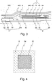
- Fig. 3 shows a cross section through a second embodiment of a circuit arrangement according to the invention.
- Fig. 4 shows a plan view of the second embodiment of the circuit arrangement according to the invention.
- Fig. 5 shows a cross section through a third embodiment of a circuit arrangement according to the invention.
- Fig. 6 shows a cross section through a fourth embodiment of a circuit arrangement according to the invention.
- Fig. 1 shows a not to scale cross section through a first embodiment of a circuit arrangement according to the invention.
- a substrate (2) as it is often known as so-called.
- DCB direct copper bonding
- IMS integrated metal substrate
- Shown is an insulating layer (20) arranged thereon conductor tracks (22 a / b) of the substrate (2).
- One of these conductor tracks (22a) carries here a preferably unhoused semiconductor component (3), for example a power transistor as it is often used to drive three-phase motors.
- a sintered metal surface (52) is arranged for the electrically conductive connection between the first conductor track (22a) carrying the semiconductor component and a contact area (32) on the first main face of the semiconductor component (3).
- This sintered metal surface (52) represents an electrically conductive connection of high reliability by the pressure sintering process of manufacture.
- the second main surface of the semiconductor device has two contact surfaces (34, 36).
- This connecting device (4) is designed here as a metallic foil (40), preferably made of copper with a noble metal coating in the region (500, 540) of the sintered connections (50, 54).
- the thickness of this metallic foil (40) is chosen such that it has at least the same current carrying capacity as a Drahtbonditati according to the prior art.
- connection device (4) represents the electrical connection between the second main area or the second contact area (34) of the semiconductor component (3) and a second conductor track (22b) of the substrate (2).
- the connection to the second conductor track (22b) is likewise designed as a pressure sintered connection.
- the metallic foil (40) has an arcuate course (46) between the two contact surfaces (500, 540).
- an insulating material (6) is arranged in the volume region formed by the arcuate course (400) of the connecting device (4), the substrate (2) and the semiconductor component (3).
- This insulating material (6) was applied during the manufacturing process in that area which is subsequently covered by a connecting device (4). In this embodiment, this is the region of an edge (30) of the semiconductor component (3).
- the insulating material (6) used is preferably a multicomponent silicone compound which has been applied in a casting process to the edge of the semiconductor component (3) and crosslinked by means of UV exposure.
- a certain toughness of the insulating material (6) is given, and on the other hand, such a silicone compound is also suitable for internal insulation, if the circuit arrangement has been designed for correspondingly high voltages.
- Fig. 2 shows a plan view of the first embodiment of the circuit arrangement according to the invention. Shown here are the same parts of the circuit as under Fig. 1 described.
- connection device (4) which projects beyond the edge of the semiconductor component of the edge facing the insulating material (6) and establishes the connection to the second conductor track (22b) there, is not explicitly shown.
- the insulating material (6) serves on the one hand in a two-dimensional pressure introduction in the context of the pressure sintered connection in the direction of the plane of the drawing as quasihydostatic element, which evenly distributes the pressure at its interfaces and thus prevents damage to the semiconductor device (3) during pressurization.
- the insulating material (6) also serves the already described electrical insulation of the circuit arrangement according to the invention.
- Fig. 3 shows a cross section through a second embodiment of a circuit arrangement according to the invention.
- the substrate (2) is identical to that in FIG Fig. 1 , In this embodiment, however, the semiconductor device (3) is designed as a power thyristor in MESA structure.
- the connecting device (4) has here in addition to a first metallic foil (40) as in Fig. 1 4 shows yet another metallic foil (42) separated from the first (40) by an insulating foil (44).
- This film composite extends the functionality of the connecting device (4) by way of example by a line for gate control and, if necessary, by further lines, preferably in the region of the second metallic foil (42).
- the connecting device (4) projects beyond the semiconductor component (3) at more than one edge.
- a plurality of semiconductor components (3) can be selectively activated.
- the insulating material it is preferable for the insulating material to completely surround the edge of the semiconductor component (3), as in FIG Fig. 4 shown, but here has been dispensed with the representation of the connecting device.
- Fig. 5 shows a cross section through a third embodiment of a circuit arrangement according to the invention. This is in contrast to the embodiment according to Fig. 1 the electrically conductive connection between the connecting device (4) and the second contact surface (34) of the semiconductor component (3) is formed as a spot-welded connection of embossing nubs (46) of the metallic foil (40).
- the connecting device (4) is arranged on the substrate (2) together with semiconductor components (3) arranged thereon during the production process.
- the insulation material (6) serves as an intermediate layer between the metallic foil (40) of the connecting device (4) and the semiconductor component (3).
- Fig. 6 shows a cross section through a fourth embodiment of a circuit arrangement according to the invention.
- the connecting device (4) establishes a connection between a contact surface (34) of a semiconductor device (3) and a not on the substrate (2) arranged contact surface, for example on a connecting element, not shown, for external connection forth.
- the insulating material in the volume limited by the substrate (2), the connecting device (4) itself and the semiconductor device (3) is arranged.
Landscapes
- Wire Bonding (AREA)
- Coupling Device And Connection With Printed Circuit (AREA)
- Use Of Switch Circuits For Exchanges And Methods Of Control Of Multiplex Exchanges (AREA)
- Electric Connection Of Electric Components To Printed Circuits (AREA)
- Structures Or Materials For Encapsulating Or Coating Semiconductor Devices Or Solid State Devices (AREA)
Abstract
Description
- Die Erfindung beschreibt eine Schaltungsanordnung mit Verbindungseinrichtung zur elektrisch leitenden Verbindung von Halbleiterbauelementen mit den Leiterbahnen eines Substrats, wobei die Verbindungseinrichtung mit einer metallischen Folie ausgebildet ist. Weiterhin wird ein vorteilhaftes Verfahren zur Herstellung einer derartigen Schaltungsanordnung beschrieben.
- Es ist eine Vielzahl von Verbindungseinrichtungen für elektronische Bauelemente bekannt. Bei gehausten Bauelementen sind beispielhaft metallische Verbindungseinrichtungen und deren löttechnische Verbindung mit Substraten bekannt, wobei hier unter Substraten auch jegliche Art von Leiterplatten verstanden werden soll.
- Bei ungehausten Bauelementen ist als Verbindungseinrichtung die Drahtbondverbindung weit verbreitet. Im Bereich von Leistungshalbleitermodulen sind weiterhin formschlüssige Verbindungen, als sog. Druckkontaktierung bekannt. Ebenfalls von Leistungshalbleitermodulen sind druckkontaktierte flexible Leiterplatten als Verbindungseinrichtungen bekannt. Die
DE 102 21 970 A1 offenbart ein Leistungshalbleitermodul mit einer derartigen Verbindungseinrichtung, lässt allerdings deren exakte Ausgestaltung offen. - Die
DE 103 55 925 A1 offenbart eine Verbindungseinrichtung für Leistungshalbleiterbauelemente bestehend aus einem Folienverbund einer ersten und einer zweiten elektrisch leitenden Folie mit einer isolierenden Zwischenlage. Die Leistungshalbleiterbauelemente sind mit der ersten leitenden Schicht mittels Ultraschallschweißen dauerhaft sicher elektrisch verbunden. Die modulinterne schaltungsgerechte Verbindung der Leistungshalbleiterbauelemente mit Leiterbahnen eines Substrats ist hierbei mittels metallischer Kontaktelemente ausgebildet deren Dicke derjenigen der Leistungshalbleiterbauelemente angepassten ist. Diese Kontaktelemente werden ebenfalls wie die Leistungshalbleiterbauelemente mittels Ultraschallschweißen mit der Verbindungseinrichtung verbunden. - Die leitende Folie zur Ultraschallschweißverbindung mit Leistungshalbleiterbauelement und Kontaktelemente besteht hierbei aus Aluminium mit Prägenoppen, da Aluminium eine vorzügliche Schweißverbindung mit der ebenfalls aus einer letzten Lage Aluminium bestehenden Metallisierung des Leistungshalbleiterbauelements eingeht.
- Weiterhin sind beispielhaft aus der
DE 34 14 065 C2 und derDE 10 2004 019 567 A1 Drucksinterverfahren bekannt, welche eine dauerhafte Verbindung zwischen einem Leistungshalbleiterbauelement und einem Anschlusselement oder einem Substrat offenbaren. Das Verfahren gemäß derDE 10 2004 019 567 A1 ist gekennzeichnete durch die wesentlichen Verfahrensschritte: Aufbringen einer aus einem Metallpulver und einem Lösungsmittel bestehenden pastösen Schicht auf eine Trägerfolie; Trocknen der pastösen Schicht; Aufbringen von mindestens einem Bauelement auf die getrocknete Schicht; Druckbeaufschlagung des Verbundes aus dem Bauelement und der Trägerfolie mit der getrockneten Schicht, wodurch die Haftkraft zwischen der Schicht und dem Bauelement größer wird als zwischen der Schicht und der Trägerfolie (10); Abheben des mindestens einen Bauelements mit daran haftender Schicht von der Trägerfolie; Positionierung des Bauelements mit der daran haftenden Schicht auf dem Substrat; Druckbeaufschlagung der Anordnung des Substrats und des Bauelements zu deren Sinterverbindung. - Der Erfindung liegt die Aufgabe zugrunde eine Schaltungsanordnung mit Verbindungseinrichtung für die Verbindung mindestens eines Halbleiterbauelements beispielhaft mit einer Leiterbahn eines Substrats sowie derer Herstellungsverfahren vorzustellen, wobei diese Schaltungsanordnung einer einfachen Herstellung zugänglich ist und die elektrischen Verbindungen innerhalb dieser Schaltungsanordnung eine hohe Zuverlässigkeit aufweisen.
- Diese Aufgabe wird erfindungsgemäß gelöst, durch Schaltungsanordnung gemäß Anspruch 1 sowie durch ein Herstellungsverfahren gemäß Anspruch 8. Bevorzugte Ausführungsformen sind in den Unteransprüchen beschrieben.
- Ausgangspunkt der erfindungsgemäßen Schaltungsanordnung ist ein Substrat mit auf einer Hauptfläche angeordneten Leiterbahnen. Auf diesen Leiterbahnen ist mindestens ein Halbleiterbauelement angeordnet. Die erste Kontaktfläche auf der ersten Hauptfläche dieses Halbleiterbauelements ist hierzu mit einer ersten Leiterbahn des Substrats, vorzugsweise elektrisch leitend, verbunden. Vorteilhafterweise ist diese Verbindung als Drucksinterverbindung ausgebildet.
- Die Schaltungsanordnung weist weiterhin eine elektrisch leitfähige Verbindungseinrichtung zwischen mindestens einer Kontaktfläche auf der zweiten Hauptfläche des Halbleiterbauelement und beispielhaft einer zweiten Leiterbahn auf. Hierbei ist die elektrische Verbindung zwischen der Verbindungseinrichtung und der zweiten Leiterbahn ebenfalls als Drucksinterverbindung ausgebildet.
- Besonders vorteilhaft ist es, wenn auch die elektrisch leitende Verbindung der Kontaktflächen der zweiten Hauptfläche des Halbleiterbauelements mit der Verbindungseinrichtung als Drucksinterverbindungen ausgebildet sind. Für die Ausbildung dieser Drucksinterverbindungen innerhalb der genannten Schaltungsanordnung weist das Herstellungsverfahren mit den folgenden wesentlichen Schritten besondere Vorteile auf:
- Ausbildung einer Mehrzahl von Sintermetallflächen auf Leiterbahnen des Substrats. Derartige Sintermetallflächen können vorzugsweise im Rahmen eines Sieb- oder Schablonendruckprozesses auf das Substrat aufgebracht werden.
- Anordnung mindestens eines Halbleiterbauelements auf einer zugeordneten Sintermetallfläche. Hierbei kann es vorteilhaft sein, wenn die zweite Hauptfläche des Halbleiterbauelements bereits ebenfalls mit einer Sintermetallfläche versehen ist.
- Anordnung des Isolierstoffes, vorzugsweise einer Silikonverbindung, speziell einem Silikonkautschuk, im Randbereich des Halbleiterbauelements. Hierbei sind speziell Spritz- oder Gießverfahren vorteilhaft an die sich eine Vernetzung beispielhaft durch UV- Belichtung anschließt.
- Anordnung der Verbindungseinrichtung. Aufbringen der Verbindungseinrichtung zur schaltungsgerechten elektrischen Verbindung der Halbleiterbauelemente und der Leiterbahnen des Substrats. Hierbei ist es vorteilhafte wenn die Verbindungseinrichtung eine hohe Funktionalität aufweist. Hierzu kann diese mehrlagig ausgebildet sein.
- Drucksinterverbindung der Verbindungseinrichtung und des Halbleiterbauelements, wodurch eine Mehrzahl von elektrisch leitenden Verbindungen gleichzeitig ausgebildet wird.
- Hierbei kommt der Anordnung des Isolierstoffes, der vorzugsweise eine Silikonverbindung ist, besondere Wichtigkeit zu. Ohne diesen Isolierstoff besteht bei der Druckbeaufschlagung im Rahmen der Drucksinterverbindung die Gefahr, dass die Ränder des Halbleiterbauelements beschädigt werden. Durch die Anordnung dieses lsolierstoffes, wird der auf ihn eingeleitete Druck an den Grenzflächen auf alle anschließenden Oberflächen quasihydrostatisch verteilt. Somit wirkt der Druck nicht nur aus Richtung der Druckeinleitung die typischerweise senkrecht zur Substratoberfläche erfolgt, sondern beaufschlagt beispielhaft den Rand des Halbleiterbauelements aus allen Richtungen annähernd gleich stark.
- Durch die geeignet Menge des lsolierstoffes füllt dieser in der Schaltungsanordnung das Volumen begrenzt durch das Substrat, der Verbindungseinrichtung und dem Halbleiterbauelement. Somit ist einerseits eine zerstörende Druckeinleitung auf den Rand des Halbleiterbauelements verhindert und andererseits eine elektrische Isolation gegeben, wobei der Isolierstoff vorteilhafterweise eine höhere Dielektrizitätskonstante als Luft aufweist.
- Besonders bevorzugte Weiterbildungen dieser Schaltungsanordnung sowie des Herstellungsverfahrens sind in der jeweiligen Beschreibung der Ausführungsbeispiele genannt. Die erfinderische Lösung wird zudem an Hand der Ausführungsbeispiele der
Fig. 1 bis 6 weiter erläutert. -
Fig. 1 zeigt einen Querschnitt durch eine erste Ausgestaltung einer erfindungsgemäßen Schaltungsanordnung. -
Fig. 2 zeigt eine Draufsicht auf die erste Ausgestaltung der erfindungsgemäßen Schaltungsanordnung. -
Fig. 3 zeigt einen Querschnitt durch eine zweite Ausgestaltung einer erfindungsgemäßen Schaltungsanordnung. -
Fig. 4 zeigt eine Draufsicht auf die zweite Ausgestaltung der erfindungsgemäßen Schaltungsanordnung. -
Fig. 5 zeigt einen Querschnitt durch eine dritte Ausgestaltung einer erfindungsgemäßen Schaltungsanordnung. -
Fig. 6 zeigt einen Querschnitt durch eine vierte Ausgestaltung einer erfindungsgemäßen Schaltungsanordnung. -
Fig. 1 zeigt einen nicht maßstäblichen Querschnitt durch eine erste Ausgestaltung einer erfindungsgemäßen Schaltungsanordnung. Dargestellt ist hierbei ein Substrat (2), wie es häufig als sog. DCB- (direct copper bonding) oder IMS- (integrated metal substrate) Substrat bekannt ist, ohne dass dieses eine Beschränkung auf derartige Substrate bedeuten soll. Dargestellt ist eine isolierende Lage (20) mit hierauf angeordneten Leiterbahnen (22 a/b) des Substrats (2). Eine dieser Leiterbahnen (22a) trägt hier ein vorzugsweise ungehaustes Halbleiterbauelement (3), beispielsweise einen Leistungstransistor wie er häufig zur Ansteuerung von Drehstrommotoren eingesetzt wird. - Zur elektrisch leitenden Verbindung zwischen der ersten das Halbleiterbauelement tragenden Leiterbahn (22a) und einer Kontaktfläche (32) auf der ersten Hauptfläche des Halbleiterbauelements (3) ist eine Sintermetallfläche (52) angeordnet. Diese Sintermetallfläche (52) stellt durch den Drucksinterprozess der Herstellung eine elektrisch leitende Verbindung hoher Zuverlässigkeit dar.
- Die zweite Hauptfläche des Halbleiterbauelements weist zwei Kontaktflächen (34, 36) auf. Eine erste großflächige Emitteranschlussfläche (34) und eine weitere kleinere Anschlussfläche (36) des Gateanschlusses. Auf der zweiten Kontaktfläche (32) ist wiederum eine Sintermetallfläche (54) angeordnet. Diese dient der elektrischen Verbindung mit einer Verbindungseinrichtung (4).
- Diese Verbindungseinrichtung (4) ist hier als metallische Folie (40), vorzugsweise aus Kupfer mit Edelmetallbeschichtung im Bereich (500, 540) der Sinterverbindungen (50, 54) ausgebildet. Die Dicke dieser metallischen Folie (40) ist derart gewählt, dass sie mindestens die gleiche Stromtragfähigkeit aufweist wie eine Drahtbondverbindung nach dem Stand der Technik.
- Die Verbindungseinrichtung (4) stellt die elektrische Verbindung zwischen der zweiten Hauptfläche bzw. der zweiten Kontaktfläche (34) des Halbleiterbauelements (3) und einer zweiten Leiterbahn (22b) des Substrats (2) dar. Die Verbindung zur zweiten Leiterbahn (22b) ist ebenfalls als Drucksinterverbindung ausgebildet. Vorzugsweise weist die metallische Folie (40) einen bogenförmigen Verlauf (46) zwischen den beiden Kontaktflächen (500, 540) auf.
- In dem Volumenbereich der durch den bogenförmigen Verlauf (400) der Verbindungseinrichtung (4), dem Substrat (2) und dem Halbleiterbauelement (3) gebildet wird ist ein lsolierstoff (6) angeordnet. Dieser lsolierstoff (6) wurde während des Herstellungsprozesses in demjenigen Bereich aufgebracht der anschließend von einer Verbindungseinrichtung (4) überdeckt wird. Bei dieser Ausgestaltung ist dies der Bereich eines Randes (30) des Halbleiterbauelements (3).
- Vorzugsweise ist der verwendete lsolierstoff (6) eine mehrkomponentige Silikonverbindung, die in einem Gießverfahren am Rand des Halbleiterbauelements (3) aufgetragen wurde und mittels einer UV- Belichtung vernetzt wurde. Somit ist einerseits eine gewisse Zähigkeit des Isolierstoffs (6) gegeben, und andererseits eignet sich eine derartige Silikonverbindung auch zur inneren Isolation, falls die Schaltungsanordnung für entsprechend hohe Spannungen entworfen wurde.
-
Fig. 2 zeigt eine Draufsicht auf die erste Ausgestaltung der erfindungsgemäßen Schaltungsanordnung. Dargestellt sind hierbei die gleichen Teile der Schaltungsanordnung wie unterFig. 1 beschrieben. - Hierbei ist die flächige Ausdehnung des lsolierstoffes (6) im Bereich zwischen den Kontaktflächen (500, 540) der Verbindungseinrichtung (4) mit der Leiterbahn (22b) sowie dem Halbleiterbauelement bzw. dessen zweiter Kontaktfläche (54) sowie auch im Bereich neben der Verbindungseinrichtung (4) dargestellt. Nicht explizit dargestellt ist die Ausbildung der Verbindungseinrichtung (4), die das Halbleiterbauelement der dem Isolierstoff (6) zugewandten Rand überragt und dort die Verbindung zur zweiten Leiterbahn (22b) herstellt.
- Gemäß dieser Ausgestaltung dient der Isolierstoff (6) einerseits bei einer flächigen Druckeinleitung im Rahmen der Drucksinterverbindung in Richtung der Zeichnungsebene als quasihydostatisches Element, das den Druck an seinen Grenzflächen gleichmäßig verteilt und somit einer Beschädigung des Halbleiterbauelement (3) während der Druckbeaufschlagung verhindert. Anderseits dient er auch der bereits beschrieben elektrischen Isolation der erfindungsgemäßen Schaltungsanordnung.
-
Fig. 3 zeigt einen Querschnitt durch eine zweite Ausgestaltung einer erfindungsgemäßen Schaltungsanordnung. Hierbei ist das Substrat (2) identisch demjenigen gemäßFig. 1 . In dieser Ausbildung ist das Halbleiterbauelement (3) allerdings als Leistungsthyristor in MESA Struktur ausgestaltet. - : Die Verbindungseinrichtung (4) weist hier zusätzlich zu einer ersten metallischen Folie (40) wie in
Fig. 1 dargestellt noch eine weitere von der ersten (40) durch eine isolierende Folie (44) getrennte metallische Folie auf (42). Dieser Folienverbund erweitert die Funktionalität der Verbindungseinrichtung (4) beispielhaft um eine Leitung zur Gateansteuerung und bei Bedarf noch um weitere Leitungen vorzugsweise im Bereich der zweiten metallischen Folie (42). - Weiterhin kann es bevorzugt sein, wie hier dargestellt, dass die Verbindungseinrichtung (4) das Halbleiterbauelement (3) an mehr als einer Rand überragt. Hierdurch kann beispielhaft eine Mehrzahl von Halbleiterbauelementen (3) selektiv angesteuert werden. Hierbei ist es bevorzugt, wenn der Isolationsstoff den Rand des Halbleiterbauelements (3) vollständig umschließt, wie in
Fig. 4 gezeigt, wobei hier allerdings auf die Darstellung der Verbindungseinrichtung verzichtet wurde. -
Fig. 5 zeigt einen Querschnitt durch eine dritte Ausgestaltung einer erfindungsgemäßen Schaltungsanordnung. Hierbei ist im Gegensatz zur Ausgestaltung gemäßFig. 1 die elektrisch leitende Verbindung zwischen der Verbindungseinrichtung (4) und der zweiten Kontaktfläche (34) des Halbleiterbauelement (3) als Punktschweißverbindung von Prägenoppen (46) der metallischen Folie (40) ausgebildet. - Hierbei wird während des Herstellungsprozesses die Verbindungseinrichtung (4) gemeinsam mit hieran angeordneten Halbleiterbauelementen (3) auf dem Substrat (2) angeordnet. Zusätzlich dient hierbei der lsolationsstoff (6) als Zwischenlage zwischen der metallischen Folie (40) der Verbindungseinrichtung (4) und dem Halbleiterbauelement (3).
-
Fig. 6 zeigt einen Querschnitt durch eine vierte Ausgestaltung einer erfindungsgemäßen Schaltungsanordnung. Im Gegensatz zur Ausgestaltung gemäßFig. 1 stellt hier die Verbindungseinrichtung (4) eine Verbindung zwischen einer Kontaktfläche (34) eines Halbleiterbauelement (3) und einer nicht auf dem Substrat (2) angeordneten Kontaktfläche, beispielsweise auf einem nicht dargestellten Anschlusselement zur externen Verbindung her. - Hierbei ist es ebenfalls bevorzugt, wenn der Isolierstoff in dem Volumen begrenzt durch das Substrat (2), die Verbindungseinrichtung (4) selbst und das Halbleiterbauelement (3) angeordnet ist.
Claims (10)
- Schaltungsanordnung mit
einem Substrat (2),
auf einer Hauptfläche dieses Substrats (2) angeordneten Leiterbahnen (22 a/b), mindestens einem mit seiner ersten Hauptfläche auf einer ersten Leiterbahn (22a) angeordnetem Halbleiterbauelement (3),
einer elektrisch leitfähigen Verbindungseinrichtung (4) zu mindestens einer Kontaktfläche (34, 36) der zweiten Hauptfläche des Halbleiterbauelement (3) wobei die Verbindung des Halbleiterbauelements (3) mit der ersten Leiterbahn (22a) und / oder der Verbindungseinrichtung (4) als Drucksinterverbindung ausgebildet ist und wobei
zwischen der Verbindungseinrichtung und einem zugeordneten Rand (30) des Halbleiterbauelements (3) ein Isolierstoff (6) angeordnet ist. - Schaltungsanordnung nach Anspruch 1,
wobei der Isolierstoff (6) als Silikonverbindung ausgebildet ist. - Schaltungsanordnung nach Anspruch 1,
wobei
eine elektrische Verbindung zwischen der Verbindungseinrichtung (4) und einer zweiten Leiterbahn (22b) als Drucksinterverbindung ausgebildet ist und hierbei in dem Volumen begrenzt durch das Substrat (2), die Verbindungseinrichtung (4) und das Halbleiterbauelement (3) der Isolierstoff (6) angeordnet ist. - Schaltungsanordnung nach Anspruch 1,
wobei die Verbindungseinrichtung (4) das Halbleiterbauelement (3) an einem Rand (30) überlappt und dort die Verbindung zur zweiten Leiterbahn (22b) ausgebildet ist. - Schaltungsanordnung nach Anspruch 1,
wobei die Verbindungseinrichtung (4) eine Mehrzahl von Halbleiterbauelementen (3) überdeckt. - Schaltungsanordnung nach Anspruch 1,
wobei die Verbindungseinrichtung (4) als metallische Folie (40) ausgebildet ist. - Schaltungsanordnung nach Anspruch 1,
wobei die Verbindungseinrichtung (4) als Folienverbund aus mindestens einer metallischen (40, 42) und einer isolierenden Folie (44) ausgebildet ist. - Verfahren zur Herstellung einer Schaltungsanordnung nach Anspruch 1 mit den wesentlichen Schritten:• Ausbildung einer Mehrzahl von Sintermetallflächen (50, 52) auf Leiterbahnen (22 a/b) des Substrats (2);• Anordnung mindestens eines Halbleiterbauelement (3) auf einer zugeordneten Sintermetallfläche (52);• Anordnung des lsolierstoffes (6) im Randbereich (30) des Halbleiterbauelements (3);• Anordnung der Verbindungseinrichtung (4);• Drucksinterverbindung der Verbindungseinrichtung (4) und des Halbleiterbauelements (3).
- Verfahren nach Anspruch 8,
wobei auf der zweiten Hauptfläche des Halbleiterbauelements (3) vor der Anordnung auf dem Substrat (2) eine Sintermetallfläche (54) ausgebildet wird. - Verfahren nach Anspruch 8,
wobei der Isolierstoff (6) in einem Spritz- oder Gießverfahren angeordnet wird.
Priority Applications (1)
| Application Number | Priority Date | Filing Date | Title |
|---|---|---|---|
| PL08000989T PL1956647T3 (pl) | 2007-02-10 | 2008-01-19 | Układ przełączający z urządzeniem połączeniowym oraz sposób jego wykonania |
Applications Claiming Priority (1)
| Application Number | Priority Date | Filing Date | Title |
|---|---|---|---|
| DE102007006706A DE102007006706B4 (de) | 2007-02-10 | 2007-02-10 | Schaltungsanordnung mit Verbindungseinrichtung sowie Herstellungsverfahren hierzu |
Publications (2)
| Publication Number | Publication Date |
|---|---|
| EP1956647A1 true EP1956647A1 (de) | 2008-08-13 |
| EP1956647B1 EP1956647B1 (de) | 2009-08-12 |
Family
ID=39322584
Family Applications (1)
| Application Number | Title | Priority Date | Filing Date |
|---|---|---|---|
| EP08000989A Active EP1956647B1 (de) | 2007-02-10 | 2008-01-19 | Schaltungsanordnung mit Verbindungseinrichtung sowie Herstellungsverfahren hierzu |
Country Status (7)
| Country | Link |
|---|---|
| EP (1) | EP1956647B1 (de) |
| AT (1) | ATE439683T1 (de) |
| DE (2) | DE102007006706B4 (de) |
| DK (1) | DK1956647T3 (de) |
| ES (1) | ES2328188T3 (de) |
| PL (1) | PL1956647T3 (de) |
| PT (1) | PT1956647E (de) |
Cited By (11)
| Publication number | Priority date | Publication date | Assignee | Title |
|---|---|---|---|---|
| DE102008033410A1 (de) * | 2008-07-16 | 2010-01-21 | Semikron Elektronik Gmbh & Co. Kg | Leistungselektronische Verbindungseinrichtung und Herstellungsverfahren hierzu |
| EP2219213A2 (de) | 2009-02-16 | 2010-08-18 | SEMIKRON Elektronik GmbH & Co. KG | Halbleiteranordnung |
| CN101859753A (zh) * | 2009-04-11 | 2010-10-13 | 赛米控电子股份有限公司 | 具有连接装置和内部接头元件的功率半导体模块 |
| DE102009020733A1 (de) * | 2009-05-11 | 2010-11-18 | Danfoss Silicon Power Gmbh | Verfahren zur Kontaktsinterung von bandförmigen Kontaktelementen |
| EP2270855A1 (de) * | 2009-06-29 | 2011-01-05 | ABB Research Ltd. | Elektrisches Modul |
| WO2010119416A3 (en) * | 2009-04-17 | 2011-08-25 | Nxp B.V. | Foil and method for foil-based clip-and/or wire-bonding and resulting package |
| CN102548223A (zh) * | 2010-12-07 | 2012-07-04 | 赛米控电子股份有限公司 | 用于制造电路布置的方法 |
| CN102867817A (zh) * | 2011-07-07 | 2013-01-09 | 赛米控电子股份有限公司 | 具有冷却装置的功率电子系统 |
| EP2743973A3 (de) * | 2012-12-11 | 2014-12-03 | Robert Bosch Gmbh | Verfahren zur Kontaktierung eines Halbleiterelements mittels Schweißens eines Kontaktelements an eine Sinterschicht auf dem Halbleiterelement und Halbleiterbauelement mit erhöhter Stabilität gegenüber thermomechanischen Einflüssen |
| WO2015018721A1 (de) * | 2013-08-07 | 2015-02-12 | Siemens Aktiengesellschaft | Leistungselektronische schaltung mit planarer elektrischer kontaktierung |
| EP4141922A1 (de) * | 2021-08-26 | 2023-03-01 | Siemens Aktiengesellschaft | Leistungselektronische baugruppe |
Families Citing this family (21)
| Publication number | Priority date | Publication date | Assignee | Title |
|---|---|---|---|---|
| DE102008017454B4 (de) | 2008-04-05 | 2010-02-04 | Semikron Elektronik Gmbh & Co. Kg | Leistungshalbleitermodul mit hermetisch dichter Schaltungsanordnung und Herstellungsverfahren hierzu |
| US8293586B2 (en) * | 2008-09-25 | 2012-10-23 | Infineon Technologies Ag | Method of manufacturing an electronic system |
| DE102009022660B3 (de) * | 2009-05-26 | 2010-09-16 | Semikron Elektronik Gmbh & Co. Kg | Befestigung eines Bauelements an einem Substrat und/oder eines Anschlusselementes an dem Bauelement und/oder an dem Substrat durch Drucksinterung |
| DE102009024370B4 (de) * | 2009-06-09 | 2014-04-30 | Semikron Elektronik Gmbh & Co. Kg | Stromrichteranordnung mit Kühleinrichtung und Herstellungsverfahren hierzu |
| DE102010011719A1 (de) | 2010-03-17 | 2011-09-22 | Semikron Elektronik Gmbh & Co. Kg | Verfahren zur Herstellung einer elektrisch leitenden Verbindung eines Kontaktes mit einem Gegenkontakt |
| DE102010039824B4 (de) | 2010-08-26 | 2018-03-29 | Semikron Elektronik Gmbh & Co. Kg | Leistungsbaugruppe mit einer flexiblen Verbindungseinrichtung |
| DE102011078806B4 (de) * | 2011-07-07 | 2014-10-30 | Semikron Elektronik Gmbh & Co. Kg | Herstellungsverfahren für ein leistungselektronisches System mit einer Kühleinrichtung |
| DE102012222012B4 (de) | 2012-11-30 | 2017-04-06 | Semikron Elektronik Gmbh & Co. Kg | Leistungshalbleitereinrichtung und ein Verfahren zur Herstellung einer Leistungshalbleitereinrichtung |
| DE102013102828B4 (de) | 2013-03-20 | 2018-04-12 | Semikron Elektronik Gmbh & Co. Kg | Leistungsbaugruppe mit einer als Folienverbund ausgebildeten Verbindungseinrichtung |
| DE102013104949B3 (de) | 2013-05-14 | 2014-04-24 | Semikron Elektronik Gmbh & Co. Kg | Leistungselektronische Schalteinrichtung und Anordnung hiermit |
| DE102013108185B4 (de) | 2013-07-31 | 2021-09-23 | Semikron Elektronik Gmbh & Co. Kg | Verfahren zur Herstellung einer leistungselektronischen Schalteinrichtung und leistungselektronische Schalteinrichtung |
| DE102015103779A1 (de) * | 2015-03-16 | 2016-09-22 | Pac Tech-Packaging Technologies Gmbh | Chipanordnung und Verfahren zur Ausbildung einer Kontaktverbindung |
| DE102015116165A1 (de) | 2015-09-24 | 2017-03-30 | Semikron Elektronik Gmbh & Co. Kg | Verfahren zur Herstellung einer leistungselektronischen Schalteinrichtung und leistungselektronische Schalteinrichtung |
| DE102015120156B4 (de) | 2015-11-20 | 2019-07-04 | Semikron Elektronik Gmbh & Co. Kg | Vorrichtung zur materialschlüssigen Verbindung von Verbindungspartnern eines Leistungselekronik-Bauteils und Verwendung einer solchen Vorrichtung |
| DE102015120157A1 (de) | 2015-11-20 | 2017-05-24 | Semikron Elektronik Gmbh & Co. Kg | Leistungselektronische Schalteinrichtung mit einer Mehrzahl von Potentialflächen |
| DE102015120154B4 (de) | 2015-11-20 | 2023-02-09 | Semikron Elektronik Gmbh & Co. Kg | Leistungshalbleitereinrichtung mit einem Substrat und einem Leistungshalbleiterbauelement |
| DE102019113762B4 (de) * | 2019-05-23 | 2022-04-14 | Semikron Elektronik Gmbh & Co. Kg | Verfahren zur Herstellung eines Leistungshalbleitermoduls |
| DE102019126623B4 (de) * | 2019-10-02 | 2024-03-14 | Semikron Elektronik Gmbh & Co. Kg Patentabteilung | Leistungselektronische Schalteinrichtung mit einer Vergussmasse |
| DE102020121033B4 (de) | 2020-08-10 | 2024-08-29 | Semikron Elektronik Gmbh & Co. Kg | Leistungselektronische Schalteinrichtung, Leistungshalbleitermodul damit und Verfahren zur Herstellung |
| DE102020122784B4 (de) | 2020-09-01 | 2022-04-28 | Semikron Elektronik Gmbh & Co. Kg | Leistungselektronische Schalteinrichtung mit einem dreidimensional vorgeformten Isolationsformkörper und Verfahren zu deren Herstellung |
| DE102022111579A1 (de) | 2022-05-10 | 2023-11-16 | Semikron Elektronik Gmbh & Co. Kg | Verfahren zur Herstellung einer leistungselektronischen Schalteinrichtung und leistungselektronische Schalteinrichtung |
Citations (6)
| Publication number | Priority date | Publication date | Assignee | Title |
|---|---|---|---|---|
| DE3414065C2 (de) | 1984-04-13 | 1989-07-27 | Siemens Ag, 1000 Berlin Und 8000 Muenchen, De | |
| WO2003030247A2 (de) | 2001-09-28 | 2003-04-10 | Siemens Aktiengesellschaft | Verfahren zum kontaktieren elektrischer kontaktflächen eines substrats und vorrichtung aus einem substrat mit elektrischen kontaktflächen |
| US20040227235A1 (en) | 2003-03-13 | 2004-11-18 | Seiko Epson Corporation | Electronic device and method of manufacturing the same, circuit board, and electronic instrument |
| DE10355925A1 (de) | 2003-11-29 | 2005-06-30 | Semikron Elektronik Gmbh | Leistungshalbleitermodul und Verfahren seiner Herstellung |
| DE102004019567B3 (de) | 2004-04-22 | 2006-01-12 | Semikron Elektronik Gmbh & Co. Kg | Verfahren zur Befestigung von elektronischen Bauelementen auf einem Substrat |
| US20060103000A1 (en) * | 2004-11-16 | 2006-05-18 | Seiko Epson Corporation | Electronic device package and electronic equipment |
Family Cites Families (5)
| Publication number | Priority date | Publication date | Assignee | Title |
|---|---|---|---|---|
| DE19617055C1 (de) * | 1996-04-29 | 1997-06-26 | Semikron Elektronik Gmbh | Halbleiterleistungsmodul hoher Packungsdichte in Mehrschichtbauweise |
| DE10121970B4 (de) * | 2001-05-05 | 2004-05-27 | Semikron Elektronik Gmbh | Leistungshalbleitermodul in Druckkontaktierung |
| DE10221970A1 (de) | 2002-05-17 | 2003-11-27 | Deutsche Telekom Ag | Optischer Detektor mit Auflösung im Nanometerbereich |
| DE102004057421B4 (de) * | 2004-11-27 | 2009-07-09 | Semikron Elektronik Gmbh & Co. Kg | Druckkontaktiertes Leistungshalbleitermodul für hohe Umgebungstemperaturen und Verfahren zu seiner Herstellung |
| DE102005047567B3 (de) * | 2005-10-05 | 2007-03-29 | Semikron Elektronik Gmbh & Co. Kg | Leistungshalbleitermodul mit Isolationszwischenlage und Verfahren zu seiner Herstellung |
-
2007
- 2007-02-10 DE DE102007006706A patent/DE102007006706B4/de active Active
-
2008
- 2008-01-19 DE DE502008000072T patent/DE502008000072D1/de active Active
- 2008-01-19 EP EP08000989A patent/EP1956647B1/de active Active
- 2008-01-19 ES ES08000989T patent/ES2328188T3/es active Active
- 2008-01-19 AT AT08000989T patent/ATE439683T1/de active
- 2008-01-19 PT PT08000989T patent/PT1956647E/pt unknown
- 2008-01-19 PL PL08000989T patent/PL1956647T3/pl unknown
- 2008-01-19 DK DK08000989T patent/DK1956647T3/da active
Patent Citations (6)
| Publication number | Priority date | Publication date | Assignee | Title |
|---|---|---|---|---|
| DE3414065C2 (de) | 1984-04-13 | 1989-07-27 | Siemens Ag, 1000 Berlin Und 8000 Muenchen, De | |
| WO2003030247A2 (de) | 2001-09-28 | 2003-04-10 | Siemens Aktiengesellschaft | Verfahren zum kontaktieren elektrischer kontaktflächen eines substrats und vorrichtung aus einem substrat mit elektrischen kontaktflächen |
| US20040227235A1 (en) | 2003-03-13 | 2004-11-18 | Seiko Epson Corporation | Electronic device and method of manufacturing the same, circuit board, and electronic instrument |
| DE10355925A1 (de) | 2003-11-29 | 2005-06-30 | Semikron Elektronik Gmbh | Leistungshalbleitermodul und Verfahren seiner Herstellung |
| DE102004019567B3 (de) | 2004-04-22 | 2006-01-12 | Semikron Elektronik Gmbh & Co. Kg | Verfahren zur Befestigung von elektronischen Bauelementen auf einem Substrat |
| US20060103000A1 (en) * | 2004-11-16 | 2006-05-18 | Seiko Epson Corporation | Electronic device package and electronic equipment |
Cited By (22)
| Publication number | Priority date | Publication date | Assignee | Title |
|---|---|---|---|---|
| DE102008033410A1 (de) * | 2008-07-16 | 2010-01-21 | Semikron Elektronik Gmbh & Co. Kg | Leistungselektronische Verbindungseinrichtung und Herstellungsverfahren hierzu |
| DE102008033410B4 (de) * | 2008-07-16 | 2011-06-30 | SEMIKRON Elektronik GmbH & Co. KG, 90431 | Leistungselektronische Verbindungseinrichtung mit einem Leistungshalbleiterbauelement und Herstellungsverfahren hierzu |
| EP2219213A2 (de) | 2009-02-16 | 2010-08-18 | SEMIKRON Elektronik GmbH & Co. KG | Halbleiteranordnung |
| EP2219213A3 (de) * | 2009-02-16 | 2010-11-03 | SEMIKRON Elektronik GmbH & Co. KG | Halbleiteranordnung |
| US8564126B2 (en) | 2009-02-16 | 2013-10-22 | Semikron Elektronik Gmbh & Co. Kg | Semiconductor arrangement |
| US8247899B2 (en) | 2009-04-11 | 2012-08-21 | Semikron Elektronik Gmbh & Co. Kg | Power semiconductor module comprising a connection device with internal contact spring connection elements |
| CN101859753A (zh) * | 2009-04-11 | 2010-10-13 | 赛米控电子股份有限公司 | 具有连接装置和内部接头元件的功率半导体模块 |
| EP2239768A1 (de) * | 2009-04-11 | 2010-10-13 | SEMIKRON Elektronik GmbH & Co. KG | Leistungshalbleitermodul mit einer Verbindungseinrichtung und mit als Kontaktfeder ausgebildeten internen Hilfanschlusselementen |
| CN101859753B (zh) * | 2009-04-11 | 2014-06-04 | 赛米控电子股份有限公司 | 具有连接装置和内部接头元件的功率半导体模块 |
| WO2010119416A3 (en) * | 2009-04-17 | 2011-08-25 | Nxp B.V. | Foil and method for foil-based clip-and/or wire-bonding and resulting package |
| DE102009020733A1 (de) * | 2009-05-11 | 2010-11-18 | Danfoss Silicon Power Gmbh | Verfahren zur Kontaktsinterung von bandförmigen Kontaktelementen |
| DE102009020733B4 (de) * | 2009-05-11 | 2011-12-08 | Danfoss Silicon Power Gmbh | Verfahren zur Kontaktsinterung von bandförmigen Kontaktelementen |
| EP2270855A1 (de) * | 2009-06-29 | 2011-01-05 | ABB Research Ltd. | Elektrisches Modul |
| EP2463900A3 (de) * | 2010-12-07 | 2012-08-15 | SEMIKRON Elektronik GmbH & Co. KG | Verfahren zur Herstellung einer Schaltungsanordnung |
| CN102548223A (zh) * | 2010-12-07 | 2012-07-04 | 赛米控电子股份有限公司 | 用于制造电路布置的方法 |
| CN102548223B (zh) * | 2010-12-07 | 2016-08-17 | 赛米控电子股份有限公司 | 用于制造电路布置的方法 |
| CN102867817A (zh) * | 2011-07-07 | 2013-01-09 | 赛米控电子股份有限公司 | 具有冷却装置的功率电子系统 |
| CN102867817B (zh) * | 2011-07-07 | 2017-05-10 | 赛米控电子股份有限公司 | 具有冷却装置的功率电子系统 |
| EP2743973A3 (de) * | 2012-12-11 | 2014-12-03 | Robert Bosch Gmbh | Verfahren zur Kontaktierung eines Halbleiterelements mittels Schweißens eines Kontaktelements an eine Sinterschicht auf dem Halbleiterelement und Halbleiterbauelement mit erhöhter Stabilität gegenüber thermomechanischen Einflüssen |
| WO2015018721A1 (de) * | 2013-08-07 | 2015-02-12 | Siemens Aktiengesellschaft | Leistungselektronische schaltung mit planarer elektrischer kontaktierung |
| EP4141922A1 (de) * | 2021-08-26 | 2023-03-01 | Siemens Aktiengesellschaft | Leistungselektronische baugruppe |
| WO2023025457A1 (de) * | 2021-08-26 | 2023-03-02 | Siemens Aktiengesellschaft | Leistungselektronische baugruppe |
Also Published As
| Publication number | Publication date |
|---|---|
| DE102007006706A1 (de) | 2008-08-21 |
| PT1956647E (pt) | 2009-12-07 |
| ES2328188T3 (es) | 2009-11-10 |
| DK1956647T3 (da) | 2009-11-09 |
| ATE439683T1 (de) | 2009-08-15 |
| DE502008000072D1 (de) | 2009-09-24 |
| EP1956647B1 (de) | 2009-08-12 |
| PL1956647T3 (pl) | 2009-12-31 |
| DE102007006706B4 (de) | 2011-05-26 |
Similar Documents
| Publication | Publication Date | Title |
|---|---|---|
| EP1956647B1 (de) | Schaltungsanordnung mit Verbindungseinrichtung sowie Herstellungsverfahren hierzu | |
| DE102008017454B4 (de) | Leistungshalbleitermodul mit hermetisch dichter Schaltungsanordnung und Herstellungsverfahren hierzu | |
| EP1255299B1 (de) | Leistungshalbleitermodul in Druckkontaktierung | |
| EP1841299A2 (de) | Verbindungseinrichtung für elektronishche Bauelemente | |
| EP1772900B1 (de) | Herstellungsverfahren einer Anordnung mit Leistungshalbleiterbauelementen, welches einen Schritt Drucksintern beinhaltet | |
| EP1393605B1 (de) | Leiterplatte mit mindestens einem elektronischen bauteil | |
| DE102012206758B3 (de) | Verfahren zur Herstellung eines Substrats und ein Leistungshalbleitermodul mit einem Substrat für mindestens ein Leitungshalbleiterbauelement | |
| EP1772902B1 (de) | Leistungshalbleitermodul mit Isolationszwischenlage und Verfahren zu seiner Herstellung | |
| EP2061071A2 (de) | Verfahren zur Herstellung einer Halbleiterbaugruppe | |
| DE3930858C2 (de) | Modulaufbau | |
| DE102008033410B4 (de) | Leistungselektronische Verbindungseinrichtung mit einem Leistungshalbleiterbauelement und Herstellungsverfahren hierzu | |
| DE102011078806B4 (de) | Herstellungsverfahren für ein leistungselektronisches System mit einer Kühleinrichtung | |
| DE102008026347B4 (de) | Leistungselektronische Anordnung mit einem Substrat und einem Grundkörper | |
| DE10059808A1 (de) | Verfahren zur Verbindung einer integrierten Schaltung und einer flexiblen Schaltung | |
| DE102011004543B4 (de) | Widerstand, Leiterplatte und elektrisches oder elektronisches Gerät | |
| EP1993132A2 (de) | Leistungshalbleitersubstrat mit Metallkontaktschicht sowie Herstellungsverfahren hierzu | |
| DE102014203306A1 (de) | Herstellen eines Elektronikmoduls | |
| DE102016214310B4 (de) | Schaltungsträger, Leistungsschaltungsanordnung mit einem Schaltungsträger, Verfahren zum Herstellen eines Schaltungsträgers | |
| DE10121969C1 (de) | Schaltungsanordnung in Druckkontaktierung und Verfahren zu seiner Herstellung | |
| DE102016101726B4 (de) | Leistungshalbleitereinrichtung und Verfahren zur Herstellung einer Leistungshalbleitereinrichtung | |
| DE102012213555A1 (de) | Verfahren zur Herstellung eines Substrats für ein Leistungshalbleiterbauelement und Substrat | |
| DE102023113073B4 (de) | Leistungshalbleiterbauelement mit Kontakteinrichtung und Herstellungsverfahren hierfür | |
| WO2008125373A1 (de) | Verfahren zur herstellung einer leiterbahnstruktur auf einer metallischen bodenplatte | |
| DE2057126C3 (de) | Anordnung und Verfahren zur Kontaktierung von Halbleiterbauelementen | |
| WO2007080027A1 (de) | Anordnung zur kühlung von leistungsbauelementen auf leiterplatten und verfahren zur herstellung derselben |
Legal Events
| Date | Code | Title | Description |
|---|---|---|---|
| PUAI | Public reference made under article 153(3) epc to a published international application that has entered the european phase |
Free format text: ORIGINAL CODE: 0009012 |
|
| 17P | Request for examination filed |
Effective date: 20080530 |
|
| AK | Designated contracting states |
Kind code of ref document: A1 Designated state(s): AT BE BG CH CY CZ DE DK EE ES FI FR GB GR HR HU IE IS IT LI LT LU LV MC MT NL NO PL PT RO SE SI SK TR |
|
| AX | Request for extension of the european patent |
Extension state: AL BA MK RS |
|
| 17Q | First examination report despatched |
Effective date: 20080918 |
|
| AKX | Designation fees paid |
Designated state(s): AT BE BG CH CY CZ DE DK EE ES FI FR GB GR HR HU IE IS IT LI LT LU LV MC MT NL NO PL PT RO SE SI SK TR |
|
| GRAP | Despatch of communication of intention to grant a patent |
Free format text: ORIGINAL CODE: EPIDOSNIGR1 |
|
| RTI1 | Title (correction) |
Free format text: CIRCUIT ARRANGEMENT WITH CONNECTING DEVICE AND CORRESPONDING PRODUCTION METHOD |
|
| GRAS | Grant fee paid |
Free format text: ORIGINAL CODE: EPIDOSNIGR3 |
|
| GRAA | (expected) grant |
Free format text: ORIGINAL CODE: 0009210 |
|
| AK | Designated contracting states |
Kind code of ref document: B1 Designated state(s): AT BE BG CH CY CZ DE DK EE ES FI FR GB GR HR HU IE IS IT LI LT LU LV MC MT NL NO PL PT RO SE SI SK TR |
|
| REG | Reference to a national code |
Ref country code: GB Ref legal event code: FG4D Free format text: NOT ENGLISH |
|
| REG | Reference to a national code |
Ref country code: CH Ref legal event code: EP |
|
| REG | Reference to a national code |
Ref country code: CH Ref legal event code: NV Representative=s name: BRAUNPAT BRAUN EDER AG |
|
| REG | Reference to a national code |
Ref country code: IE Ref legal event code: FG4D |
|
| REF | Corresponds to: |
Ref document number: 502008000072 Country of ref document: DE Date of ref document: 20090924 Kind code of ref document: P |
|
| REG | Reference to a national code |
Ref country code: DK Ref legal event code: T3 |
|
| REG | Reference to a national code |
Ref country code: ES Ref legal event code: FG2A Ref document number: 2328188 Country of ref document: ES Kind code of ref document: T3 |
|
| REG | Reference to a national code |
Ref country code: SE Ref legal event code: TRGR |
|
| REG | Reference to a national code |
Ref country code: PT Ref legal event code: SC4A Free format text: AVAILABILITY OF NATIONAL TRANSLATION Effective date: 20091127 |
|
| REG | Reference to a national code |
Ref country code: PL Ref legal event code: T3 |
|
| LTIE | Lt: invalidation of european patent or patent extension |
Effective date: 20090812 |
|
| PG25 | Lapsed in a contracting state [announced via postgrant information from national office to epo] |
Ref country code: LT Free format text: LAPSE BECAUSE OF FAILURE TO SUBMIT A TRANSLATION OF THE DESCRIPTION OR TO PAY THE FEE WITHIN THE PRESCRIBED TIME-LIMIT Effective date: 20090812 Ref country code: NO Free format text: LAPSE BECAUSE OF FAILURE TO SUBMIT A TRANSLATION OF THE DESCRIPTION OR TO PAY THE FEE WITHIN THE PRESCRIBED TIME-LIMIT Effective date: 20091112 Ref country code: IS Free format text: LAPSE BECAUSE OF FAILURE TO SUBMIT A TRANSLATION OF THE DESCRIPTION OR TO PAY THE FEE WITHIN THE PRESCRIBED TIME-LIMIT Effective date: 20091212 |
|
| PG25 | Lapsed in a contracting state [announced via postgrant information from national office to epo] |
Ref country code: LV Free format text: LAPSE BECAUSE OF FAILURE TO SUBMIT A TRANSLATION OF THE DESCRIPTION OR TO PAY THE FEE WITHIN THE PRESCRIBED TIME-LIMIT Effective date: 20090812 Ref country code: SI Free format text: LAPSE BECAUSE OF FAILURE TO SUBMIT A TRANSLATION OF THE DESCRIPTION OR TO PAY THE FEE WITHIN THE PRESCRIBED TIME-LIMIT Effective date: 20090812 Ref country code: HR Free format text: LAPSE BECAUSE OF FAILURE TO SUBMIT A TRANSLATION OF THE DESCRIPTION OR TO PAY THE FEE WITHIN THE PRESCRIBED TIME-LIMIT Effective date: 20090812 |
|
| REG | Reference to a national code |
Ref country code: IE Ref legal event code: FD4D |
|
| PG25 | Lapsed in a contracting state [announced via postgrant information from national office to epo] |
Ref country code: BG Free format text: LAPSE BECAUSE OF FAILURE TO SUBMIT A TRANSLATION OF THE DESCRIPTION OR TO PAY THE FEE WITHIN THE PRESCRIBED TIME-LIMIT Effective date: 20091112 |
|
| REG | Reference to a national code |
Ref country code: SK Ref legal event code: T3 Ref document number: E 6575 Country of ref document: SK |
|
| PG25 | Lapsed in a contracting state [announced via postgrant information from national office to epo] |
Ref country code: CZ Free format text: LAPSE BECAUSE OF FAILURE TO SUBMIT A TRANSLATION OF THE DESCRIPTION OR TO PAY THE FEE WITHIN THE PRESCRIBED TIME-LIMIT Effective date: 20090812 Ref country code: RO Free format text: LAPSE BECAUSE OF FAILURE TO SUBMIT A TRANSLATION OF THE DESCRIPTION OR TO PAY THE FEE WITHIN THE PRESCRIBED TIME-LIMIT Effective date: 20090812 Ref country code: EE Free format text: LAPSE BECAUSE OF FAILURE TO SUBMIT A TRANSLATION OF THE DESCRIPTION OR TO PAY THE FEE WITHIN THE PRESCRIBED TIME-LIMIT Effective date: 20090812 Ref country code: IE Free format text: LAPSE BECAUSE OF FAILURE TO SUBMIT A TRANSLATION OF THE DESCRIPTION OR TO PAY THE FEE WITHIN THE PRESCRIBED TIME-LIMIT Effective date: 20090812 |
|
| PLBE | No opposition filed within time limit |
Free format text: ORIGINAL CODE: 0009261 |
|
| STAA | Information on the status of an ep patent application or granted ep patent |
Free format text: STATUS: NO OPPOSITION FILED WITHIN TIME LIMIT |
|
| 26N | No opposition filed |
Effective date: 20100517 |
|
| BERE | Be: lapsed |
Owner name: SEMIKRON ELEKTRONIK G.M.B.H. & CO. KG Effective date: 20100131 |
|
| PG25 | Lapsed in a contracting state [announced via postgrant information from national office to epo] |
Ref country code: MC Free format text: LAPSE BECAUSE OF NON-PAYMENT OF DUE FEES Effective date: 20100131 |
|
| PG25 | Lapsed in a contracting state [announced via postgrant information from national office to epo] |
Ref country code: GR Free format text: LAPSE BECAUSE OF FAILURE TO SUBMIT A TRANSLATION OF THE DESCRIPTION OR TO PAY THE FEE WITHIN THE PRESCRIBED TIME-LIMIT Effective date: 20091113 |
|
| PG25 | Lapsed in a contracting state [announced via postgrant information from national office to epo] |
Ref country code: BE Free format text: LAPSE BECAUSE OF NON-PAYMENT OF DUE FEES Effective date: 20100131 |
|
| PG25 | Lapsed in a contracting state [announced via postgrant information from national office to epo] |
Ref country code: MT Free format text: LAPSE BECAUSE OF FAILURE TO SUBMIT A TRANSLATION OF THE DESCRIPTION OR TO PAY THE FEE WITHIN THE PRESCRIBED TIME-LIMIT Effective date: 20090812 |
|
| PG25 | Lapsed in a contracting state [announced via postgrant information from national office to epo] |
Ref country code: CY Free format text: LAPSE BECAUSE OF FAILURE TO SUBMIT A TRANSLATION OF THE DESCRIPTION OR TO PAY THE FEE WITHIN THE PRESCRIBED TIME-LIMIT Effective date: 20090812 |
|
| PG25 | Lapsed in a contracting state [announced via postgrant information from national office to epo] |
Ref country code: HU Free format text: LAPSE BECAUSE OF FAILURE TO SUBMIT A TRANSLATION OF THE DESCRIPTION OR TO PAY THE FEE WITHIN THE PRESCRIBED TIME-LIMIT Effective date: 20100213 Ref country code: LU Free format text: LAPSE BECAUSE OF NON-PAYMENT OF DUE FEES Effective date: 20100119 |
|
| PG25 | Lapsed in a contracting state [announced via postgrant information from national office to epo] |
Ref country code: TR Free format text: LAPSE BECAUSE OF FAILURE TO SUBMIT A TRANSLATION OF THE DESCRIPTION OR TO PAY THE FEE WITHIN THE PRESCRIBED TIME-LIMIT Effective date: 20090812 |
|
| REG | Reference to a national code |
Ref country code: FR Ref legal event code: PLFP Year of fee payment: 9 |
|
| REG | Reference to a national code |
Ref country code: FR Ref legal event code: PLFP Year of fee payment: 10 |
|
| PGFP | Annual fee paid to national office [announced via postgrant information from national office to epo] |
Ref country code: NL Payment date: 20170124 Year of fee payment: 10 |
|
| PGFP | Annual fee paid to national office [announced via postgrant information from national office to epo] |
Ref country code: FI Payment date: 20170120 Year of fee payment: 10 Ref country code: SE Payment date: 20170125 Year of fee payment: 10 |
|
| PGFP | Annual fee paid to national office [announced via postgrant information from national office to epo] |
Ref country code: PL Payment date: 20170116 Year of fee payment: 10 Ref country code: AT Payment date: 20170120 Year of fee payment: 10 Ref country code: PT Payment date: 20170104 Year of fee payment: 10 Ref country code: DK Payment date: 20170125 Year of fee payment: 10 Ref country code: SK Payment date: 20170109 Year of fee payment: 10 |
|
| REG | Reference to a national code |
Ref country code: FR Ref legal event code: PLFP Year of fee payment: 11 |
|
| REG | Reference to a national code |
Ref country code: CH Ref legal event code: PCAR Free format text: NEW ADDRESS: HOLEESTRASSE 87, 4054 BASEL (CH) |
|
| REG | Reference to a national code |
Ref country code: DK Ref legal event code: EBP Effective date: 20180131 |
|
| REG | Reference to a national code |
Ref country code: SE Ref legal event code: EUG |
|
| REG | Reference to a national code |
Ref country code: NL Ref legal event code: MM Effective date: 20180201 |
|
| REG | Reference to a national code |
Ref country code: AT Ref legal event code: MM01 Ref document number: 439683 Country of ref document: AT Kind code of ref document: T Effective date: 20180119 |
|
| REG | Reference to a national code |
Ref country code: SK Ref legal event code: MM4A Ref document number: E 6575 Country of ref document: SK Effective date: 20180119 |
|
| PG25 | Lapsed in a contracting state [announced via postgrant information from national office to epo] |
Ref country code: SE Free format text: LAPSE BECAUSE OF NON-PAYMENT OF DUE FEES Effective date: 20180120 Ref country code: PT Free format text: LAPSE BECAUSE OF NON-PAYMENT OF DUE FEES Effective date: 20180719 Ref country code: FI Free format text: LAPSE BECAUSE OF NON-PAYMENT OF DUE FEES Effective date: 20180119 |
|
| PG25 | Lapsed in a contracting state [announced via postgrant information from national office to epo] |
Ref country code: NL Free format text: LAPSE BECAUSE OF NON-PAYMENT OF DUE FEES Effective date: 20180201 Ref country code: AT Free format text: LAPSE BECAUSE OF NON-PAYMENT OF DUE FEES Effective date: 20180119 Ref country code: SK Free format text: LAPSE BECAUSE OF NON-PAYMENT OF DUE FEES Effective date: 20180119 |
|
| PG25 | Lapsed in a contracting state [announced via postgrant information from national office to epo] |
Ref country code: DK Free format text: LAPSE BECAUSE OF NON-PAYMENT OF DUE FEES Effective date: 20180131 |
|
| PG25 | Lapsed in a contracting state [announced via postgrant information from national office to epo] |
Ref country code: PL Free format text: LAPSE BECAUSE OF NON-PAYMENT OF DUE FEES Effective date: 20180119 |
|
| REG | Reference to a national code |
Ref country code: DE Ref legal event code: R081 Ref document number: 502008000072 Country of ref document: DE Owner name: SEMIKRON DANFOSS ELEKTRONIK GMBH & CO. KG, DE Free format text: FORMER OWNER: SEMIKRON ELEKTRONIK GMBH & CO. KG, 90431 NUERNBERG, DE |
|
| REG | Reference to a national code |
Ref country code: DE Ref legal event code: R079 Ref document number: 502008000072 Country of ref document: DE Free format text: PREVIOUS MAIN CLASS: H01L0021600000 Ipc: H10W0070010000 |
|
| PGFP | Annual fee paid to national office [announced via postgrant information from national office to epo] |
Ref country code: GB Payment date: 20251204 Year of fee payment: 19 |
|
| PGFP | Annual fee paid to national office [announced via postgrant information from national office to epo] |
Ref country code: FR Payment date: 20251208 Year of fee payment: 19 |
|
| REG | Reference to a national code |
Ref country code: CH Ref legal event code: U11 Free format text: ST27 STATUS EVENT CODE: U-0-0-U10-U11 (AS PROVIDED BY THE NATIONAL OFFICE) Effective date: 20260201 |
|
| PGFP | Annual fee paid to national office [announced via postgrant information from national office to epo] |
Ref country code: ES Payment date: 20260209 Year of fee payment: 19 |
|
| PGFP | Annual fee paid to national office [announced via postgrant information from national office to epo] |
Ref country code: DE Payment date: 20251203 Year of fee payment: 19 |
|
| PGFP | Annual fee paid to national office [announced via postgrant information from national office to epo] |
Ref country code: IT Payment date: 20251219 Year of fee payment: 19 |
|
| PGFP | Annual fee paid to national office [announced via postgrant information from national office to epo] |
Ref country code: CH Payment date: 20260201 Year of fee payment: 19 |