EP1993132A2 - Leistungshalbleitersubstrat mit Metallkontaktschicht sowie Herstellungsverfahren hierzu - Google Patents
Leistungshalbleitersubstrat mit Metallkontaktschicht sowie Herstellungsverfahren hierzu Download PDFInfo
- Publication number
- EP1993132A2 EP1993132A2 EP08008713A EP08008713A EP1993132A2 EP 1993132 A2 EP1993132 A2 EP 1993132A2 EP 08008713 A EP08008713 A EP 08008713A EP 08008713 A EP08008713 A EP 08008713A EP 1993132 A2 EP1993132 A2 EP 1993132A2
- Authority
- EP
- European Patent Office
- Prior art keywords
- power semiconductor
- layer
- semiconductor substrate
- contact surface
- pressurization
- Prior art date
- Legal status (The legal status is an assumption and is not a legal conclusion. Google has not performed a legal analysis and makes no representation as to the accuracy of the status listed.)
- Granted
Links
Images
Classifications
-
- H—ELECTRICITY
- H01—ELECTRIC ELEMENTS
- H01L—SEMICONDUCTOR DEVICES NOT COVERED BY CLASS H10
- H01L21/00—Processes or apparatus adapted for the manufacture or treatment of semiconductor or solid state devices or of parts thereof
- H01L21/02—Manufacture or treatment of semiconductor devices or of parts thereof
- H01L21/04—Manufacture or treatment of semiconductor devices or of parts thereof the devices having at least one potential-jump barrier or surface barrier, e.g. PN junction, depletion layer or carrier concentration layer
- H01L21/48—Manufacture or treatment of parts, e.g. containers, prior to assembly of the devices, using processes not provided for in a single one of the subgroups H01L21/06 - H01L21/326
- H01L21/4814—Conductive parts
- H01L21/4846—Leads on or in insulating or insulated substrates, e.g. metallisation
- H01L21/4867—Applying pastes or inks, e.g. screen printing
-
- C—CHEMISTRY; METALLURGY
- C04—CEMENTS; CONCRETE; ARTIFICIAL STONE; CERAMICS; REFRACTORIES
- C04B—LIME, MAGNESIA; SLAG; CEMENTS; COMPOSITIONS THEREOF, e.g. MORTARS, CONCRETE OR LIKE BUILDING MATERIALS; ARTIFICIAL STONE; CERAMICS; REFRACTORIES; TREATMENT OF NATURAL STONE
- C04B35/00—Shaped ceramic products characterised by their composition; Ceramics compositions; Processing powders of inorganic compounds preparatory to the manufacturing of ceramic products
- C04B35/622—Forming processes; Processing powders of inorganic compounds preparatory to the manufacturing of ceramic products
- C04B35/64—Burning or sintering processes
- C04B35/645—Pressure sintering
-
- C—CHEMISTRY; METALLURGY
- C04—CEMENTS; CONCRETE; ARTIFICIAL STONE; CERAMICS; REFRACTORIES
- C04B—LIME, MAGNESIA; SLAG; CEMENTS; COMPOSITIONS THEREOF, e.g. MORTARS, CONCRETE OR LIKE BUILDING MATERIALS; ARTIFICIAL STONE; CERAMICS; REFRACTORIES; TREATMENT OF NATURAL STONE
- C04B37/00—Joining burned ceramic articles with other burned ceramic articles or other articles by heating
- C04B37/02—Joining burned ceramic articles with other burned ceramic articles or other articles by heating with metallic articles
- C04B37/021—Joining burned ceramic articles with other burned ceramic articles or other articles by heating with metallic articles in a direct manner, e.g. direct copper bonding [DCB]
-
- C—CHEMISTRY; METALLURGY
- C04—CEMENTS; CONCRETE; ARTIFICIAL STONE; CERAMICS; REFRACTORIES
- C04B—LIME, MAGNESIA; SLAG; CEMENTS; COMPOSITIONS THEREOF, e.g. MORTARS, CONCRETE OR LIKE BUILDING MATERIALS; ARTIFICIAL STONE; CERAMICS; REFRACTORIES; TREATMENT OF NATURAL STONE
- C04B37/00—Joining burned ceramic articles with other burned ceramic articles or other articles by heating
- C04B37/02—Joining burned ceramic articles with other burned ceramic articles or other articles by heating with metallic articles
- C04B37/023—Joining burned ceramic articles with other burned ceramic articles or other articles by heating with metallic articles characterised by the interlayer used
- C04B37/026—Joining burned ceramic articles with other burned ceramic articles or other articles by heating with metallic articles characterised by the interlayer used consisting of metals or metal salts
-
- H—ELECTRICITY
- H01—ELECTRIC ELEMENTS
- H01L—SEMICONDUCTOR DEVICES NOT COVERED BY CLASS H10
- H01L23/00—Details of semiconductor or other solid state devices
- H01L23/34—Arrangements for cooling, heating, ventilating or temperature compensation ; Temperature sensing arrangements
- H01L23/36—Selection of materials, or shaping, to facilitate cooling or heating, e.g. heatsinks
- H01L23/373—Cooling facilitated by selection of materials for the device or materials for thermal expansion adaptation, e.g. carbon
- H01L23/3735—Laminates or multilayers, e.g. direct bond copper ceramic substrates
-
- H—ELECTRICITY
- H01—ELECTRIC ELEMENTS
- H01L—SEMICONDUCTOR DEVICES NOT COVERED BY CLASS H10
- H01L24/00—Arrangements for connecting or disconnecting semiconductor or solid-state bodies; Methods or apparatus related thereto
- H01L24/01—Means for bonding being attached to, or being formed on, the surface to be connected, e.g. chip-to-package, die-attach, "first-level" interconnects; Manufacturing methods related thereto
- H01L24/42—Wire connectors; Manufacturing methods related thereto
- H01L24/47—Structure, shape, material or disposition of the wire connectors after the connecting process
- H01L24/48—Structure, shape, material or disposition of the wire connectors after the connecting process of an individual wire connector
-
- H—ELECTRICITY
- H05—ELECTRIC TECHNIQUES NOT OTHERWISE PROVIDED FOR
- H05K—PRINTED CIRCUITS; CASINGS OR CONSTRUCTIONAL DETAILS OF ELECTRIC APPARATUS; MANUFACTURE OF ASSEMBLAGES OF ELECTRICAL COMPONENTS
- H05K3/00—Apparatus or processes for manufacturing printed circuits
- H05K3/10—Apparatus or processes for manufacturing printed circuits in which conductive material is applied to the insulating support in such a manner as to form the desired conductive pattern
- H05K3/12—Apparatus or processes for manufacturing printed circuits in which conductive material is applied to the insulating support in such a manner as to form the desired conductive pattern using thick film techniques, e.g. printing techniques to apply the conductive material or similar techniques for applying conductive paste or ink patterns
- H05K3/1283—After-treatment of the printed patterns, e.g. sintering or curing methods
-
- H—ELECTRICITY
- H05—ELECTRIC TECHNIQUES NOT OTHERWISE PROVIDED FOR
- H05K—PRINTED CIRCUITS; CASINGS OR CONSTRUCTIONAL DETAILS OF ELECTRIC APPARATUS; MANUFACTURE OF ASSEMBLAGES OF ELECTRICAL COMPONENTS
- H05K3/00—Apparatus or processes for manufacturing printed circuits
- H05K3/22—Secondary treatment of printed circuits
- H05K3/24—Reinforcing the conductive pattern
- H05K3/245—Reinforcing conductive patterns made by printing techniques or by other techniques for applying conductive pastes, inks or powders; Reinforcing other conductive patterns by such techniques
- H05K3/247—Finish coating of conductors by using conductive pastes, inks or powders
-
- C—CHEMISTRY; METALLURGY
- C04—CEMENTS; CONCRETE; ARTIFICIAL STONE; CERAMICS; REFRACTORIES
- C04B—LIME, MAGNESIA; SLAG; CEMENTS; COMPOSITIONS THEREOF, e.g. MORTARS, CONCRETE OR LIKE BUILDING MATERIALS; ARTIFICIAL STONE; CERAMICS; REFRACTORIES; TREATMENT OF NATURAL STONE
- C04B2237/00—Aspects relating to ceramic laminates or to joining of ceramic articles with other articles by heating
- C04B2237/02—Aspects relating to interlayers, e.g. used to join ceramic articles with other articles by heating
- C04B2237/12—Metallic interlayers
- C04B2237/124—Metallic interlayers based on copper
-
- C—CHEMISTRY; METALLURGY
- C04—CEMENTS; CONCRETE; ARTIFICIAL STONE; CERAMICS; REFRACTORIES
- C04B—LIME, MAGNESIA; SLAG; CEMENTS; COMPOSITIONS THEREOF, e.g. MORTARS, CONCRETE OR LIKE BUILDING MATERIALS; ARTIFICIAL STONE; CERAMICS; REFRACTORIES; TREATMENT OF NATURAL STONE
- C04B2237/00—Aspects relating to ceramic laminates or to joining of ceramic articles with other articles by heating
- C04B2237/02—Aspects relating to interlayers, e.g. used to join ceramic articles with other articles by heating
- C04B2237/12—Metallic interlayers
- C04B2237/125—Metallic interlayers based on noble metals, e.g. silver
-
- C—CHEMISTRY; METALLURGY
- C04—CEMENTS; CONCRETE; ARTIFICIAL STONE; CERAMICS; REFRACTORIES
- C04B—LIME, MAGNESIA; SLAG; CEMENTS; COMPOSITIONS THEREOF, e.g. MORTARS, CONCRETE OR LIKE BUILDING MATERIALS; ARTIFICIAL STONE; CERAMICS; REFRACTORIES; TREATMENT OF NATURAL STONE
- C04B2237/00—Aspects relating to ceramic laminates or to joining of ceramic articles with other articles by heating
- C04B2237/30—Composition of layers of ceramic laminates or of ceramic or metallic articles to be joined by heating, e.g. Si substrates
- C04B2237/32—Ceramic
- C04B2237/34—Oxidic
- C04B2237/343—Alumina or aluminates
-
- C—CHEMISTRY; METALLURGY
- C04—CEMENTS; CONCRETE; ARTIFICIAL STONE; CERAMICS; REFRACTORIES
- C04B—LIME, MAGNESIA; SLAG; CEMENTS; COMPOSITIONS THEREOF, e.g. MORTARS, CONCRETE OR LIKE BUILDING MATERIALS; ARTIFICIAL STONE; CERAMICS; REFRACTORIES; TREATMENT OF NATURAL STONE
- C04B2237/00—Aspects relating to ceramic laminates or to joining of ceramic articles with other articles by heating
- C04B2237/30—Composition of layers of ceramic laminates or of ceramic or metallic articles to be joined by heating, e.g. Si substrates
- C04B2237/40—Metallic
- C04B2237/407—Copper
-
- C—CHEMISTRY; METALLURGY
- C04—CEMENTS; CONCRETE; ARTIFICIAL STONE; CERAMICS; REFRACTORIES
- C04B—LIME, MAGNESIA; SLAG; CEMENTS; COMPOSITIONS THEREOF, e.g. MORTARS, CONCRETE OR LIKE BUILDING MATERIALS; ARTIFICIAL STONE; CERAMICS; REFRACTORIES; TREATMENT OF NATURAL STONE
- C04B2237/00—Aspects relating to ceramic laminates or to joining of ceramic articles with other articles by heating
- C04B2237/30—Composition of layers of ceramic laminates or of ceramic or metallic articles to be joined by heating, e.g. Si substrates
- C04B2237/40—Metallic
- C04B2237/408—Noble metals, e.g. palladium, platina or silver
-
- C—CHEMISTRY; METALLURGY
- C04—CEMENTS; CONCRETE; ARTIFICIAL STONE; CERAMICS; REFRACTORIES
- C04B—LIME, MAGNESIA; SLAG; CEMENTS; COMPOSITIONS THEREOF, e.g. MORTARS, CONCRETE OR LIKE BUILDING MATERIALS; ARTIFICIAL STONE; CERAMICS; REFRACTORIES; TREATMENT OF NATURAL STONE
- C04B2237/00—Aspects relating to ceramic laminates or to joining of ceramic articles with other articles by heating
- C04B2237/50—Processing aspects relating to ceramic laminates or to the joining of ceramic articles with other articles by heating
- C04B2237/70—Forming laminates or joined articles comprising layers of a specific, unusual thickness
- C04B2237/704—Forming laminates or joined articles comprising layers of a specific, unusual thickness of one or more of the ceramic layers or articles
-
- C—CHEMISTRY; METALLURGY
- C04—CEMENTS; CONCRETE; ARTIFICIAL STONE; CERAMICS; REFRACTORIES
- C04B—LIME, MAGNESIA; SLAG; CEMENTS; COMPOSITIONS THEREOF, e.g. MORTARS, CONCRETE OR LIKE BUILDING MATERIALS; ARTIFICIAL STONE; CERAMICS; REFRACTORIES; TREATMENT OF NATURAL STONE
- C04B2237/00—Aspects relating to ceramic laminates or to joining of ceramic articles with other articles by heating
- C04B2237/50—Processing aspects relating to ceramic laminates or to the joining of ceramic articles with other articles by heating
- C04B2237/70—Forming laminates or joined articles comprising layers of a specific, unusual thickness
- C04B2237/706—Forming laminates or joined articles comprising layers of a specific, unusual thickness of one or more of the metallic layers or articles
-
- C—CHEMISTRY; METALLURGY
- C04—CEMENTS; CONCRETE; ARTIFICIAL STONE; CERAMICS; REFRACTORIES
- C04B—LIME, MAGNESIA; SLAG; CEMENTS; COMPOSITIONS THEREOF, e.g. MORTARS, CONCRETE OR LIKE BUILDING MATERIALS; ARTIFICIAL STONE; CERAMICS; REFRACTORIES; TREATMENT OF NATURAL STONE
- C04B2237/00—Aspects relating to ceramic laminates or to joining of ceramic articles with other articles by heating
- C04B2237/50—Processing aspects relating to ceramic laminates or to the joining of ceramic articles with other articles by heating
- C04B2237/72—Forming laminates or joined articles comprising at least two interlayers directly next to each other
-
- H—ELECTRICITY
- H01—ELECTRIC ELEMENTS
- H01L—SEMICONDUCTOR DEVICES NOT COVERED BY CLASS H10
- H01L2224/00—Indexing scheme for arrangements for connecting or disconnecting semiconductor or solid-state bodies and methods related thereto as covered by H01L24/00
- H01L2224/01—Means for bonding being attached to, or being formed on, the surface to be connected, e.g. chip-to-package, die-attach, "first-level" interconnects; Manufacturing methods related thereto
- H01L2224/02—Bonding areas; Manufacturing methods related thereto
- H01L2224/04—Structure, shape, material or disposition of the bonding areas prior to the connecting process
- H01L2224/05—Structure, shape, material or disposition of the bonding areas prior to the connecting process of an individual bonding area
- H01L2224/0554—External layer
- H01L2224/05599—Material
- H01L2224/056—Material with a principal constituent of the material being a metal or a metalloid, e.g. boron [B], silicon [Si], germanium [Ge], arsenic [As], antimony [Sb], tellurium [Te] and polonium [Po], and alloys thereof
- H01L2224/05638—Material with a principal constituent of the material being a metal or a metalloid, e.g. boron [B], silicon [Si], germanium [Ge], arsenic [As], antimony [Sb], tellurium [Te] and polonium [Po], and alloys thereof the principal constituent melting at a temperature of greater than or equal to 950°C and less than 1550°C
- H01L2224/05644—Gold [Au] as principal constituent
-
- H—ELECTRICITY
- H01—ELECTRIC ELEMENTS
- H01L—SEMICONDUCTOR DEVICES NOT COVERED BY CLASS H10
- H01L2224/00—Indexing scheme for arrangements for connecting or disconnecting semiconductor or solid-state bodies and methods related thereto as covered by H01L24/00
- H01L2224/01—Means for bonding being attached to, or being formed on, the surface to be connected, e.g. chip-to-package, die-attach, "first-level" interconnects; Manufacturing methods related thereto
- H01L2224/42—Wire connectors; Manufacturing methods related thereto
- H01L2224/47—Structure, shape, material or disposition of the wire connectors after the connecting process
- H01L2224/48—Structure, shape, material or disposition of the wire connectors after the connecting process of an individual wire connector
- H01L2224/4805—Shape
- H01L2224/4809—Loop shape
- H01L2224/48091—Arched
-
- H—ELECTRICITY
- H01—ELECTRIC ELEMENTS
- H01L—SEMICONDUCTOR DEVICES NOT COVERED BY CLASS H10
- H01L2224/00—Indexing scheme for arrangements for connecting or disconnecting semiconductor or solid-state bodies and methods related thereto as covered by H01L24/00
- H01L2224/01—Means for bonding being attached to, or being formed on, the surface to be connected, e.g. chip-to-package, die-attach, "first-level" interconnects; Manufacturing methods related thereto
- H01L2224/42—Wire connectors; Manufacturing methods related thereto
- H01L2224/47—Structure, shape, material or disposition of the wire connectors after the connecting process
- H01L2224/48—Structure, shape, material or disposition of the wire connectors after the connecting process of an individual wire connector
- H01L2224/481—Disposition
- H01L2224/48151—Connecting between a semiconductor or solid-state body and an item not being a semiconductor or solid-state body, e.g. chip-to-substrate, chip-to-passive
- H01L2224/48221—Connecting between a semiconductor or solid-state body and an item not being a semiconductor or solid-state body, e.g. chip-to-substrate, chip-to-passive the body and the item being stacked
- H01L2224/48225—Connecting between a semiconductor or solid-state body and an item not being a semiconductor or solid-state body, e.g. chip-to-substrate, chip-to-passive the body and the item being stacked the item being non-metallic, e.g. insulating substrate with or without metallisation
- H01L2224/48227—Connecting between a semiconductor or solid-state body and an item not being a semiconductor or solid-state body, e.g. chip-to-substrate, chip-to-passive the body and the item being stacked the item being non-metallic, e.g. insulating substrate with or without metallisation connecting the wire to a bond pad of the item
-
- H—ELECTRICITY
- H01—ELECTRIC ELEMENTS
- H01L—SEMICONDUCTOR DEVICES NOT COVERED BY CLASS H10
- H01L2224/00—Indexing scheme for arrangements for connecting or disconnecting semiconductor or solid-state bodies and methods related thereto as covered by H01L24/00
- H01L2224/01—Means for bonding being attached to, or being formed on, the surface to be connected, e.g. chip-to-package, die-attach, "first-level" interconnects; Manufacturing methods related thereto
- H01L2224/42—Wire connectors; Manufacturing methods related thereto
- H01L2224/47—Structure, shape, material or disposition of the wire connectors after the connecting process
- H01L2224/48—Structure, shape, material or disposition of the wire connectors after the connecting process of an individual wire connector
- H01L2224/484—Connecting portions
- H01L2224/4847—Connecting portions the connecting portion on the bonding area of the semiconductor or solid-state body being a wedge bond
- H01L2224/48472—Connecting portions the connecting portion on the bonding area of the semiconductor or solid-state body being a wedge bond the other connecting portion not on the bonding area also being a wedge bond, i.e. wedge-to-wedge
-
- H—ELECTRICITY
- H01—ELECTRIC ELEMENTS
- H01L—SEMICONDUCTOR DEVICES NOT COVERED BY CLASS H10
- H01L2224/00—Indexing scheme for arrangements for connecting or disconnecting semiconductor or solid-state bodies and methods related thereto as covered by H01L24/00
- H01L2224/74—Apparatus for manufacturing arrangements for connecting or disconnecting semiconductor or solid-state bodies and for methods related thereto
- H01L2224/75—Apparatus for connecting with bump connectors or layer connectors
- H01L2224/7525—Means for applying energy, e.g. heating means
- H01L2224/753—Means for applying energy, e.g. heating means by means of pressure
- H01L2224/75301—Bonding head
- H01L2224/75314—Auxiliary members on the pressing surface
- H01L2224/75317—Removable auxiliary member
-
- H—ELECTRICITY
- H01—ELECTRIC ELEMENTS
- H01L—SEMICONDUCTOR DEVICES NOT COVERED BY CLASS H10
- H01L2224/00—Indexing scheme for arrangements for connecting or disconnecting semiconductor or solid-state bodies and methods related thereto as covered by H01L24/00
- H01L2224/80—Methods for connecting semiconductor or other solid state bodies using means for bonding being attached to, or being formed on, the surface to be connected
- H01L2224/85—Methods for connecting semiconductor or other solid state bodies using means for bonding being attached to, or being formed on, the surface to be connected using a wire connector
- H01L2224/8538—Bonding interfaces outside the semiconductor or solid-state body
- H01L2224/85399—Material
- H01L2224/854—Material with a principal constituent of the material being a metal or a metalloid, e.g. boron (B), silicon (Si), germanium (Ge), arsenic (As), antimony (Sb), tellurium (Te) and polonium (Po), and alloys thereof
- H01L2224/85438—Material with a principal constituent of the material being a metal or a metalloid, e.g. boron (B), silicon (Si), germanium (Ge), arsenic (As), antimony (Sb), tellurium (Te) and polonium (Po), and alloys thereof the principal constituent melting at a temperature of greater than or equal to 950°C and less than 1550°C
- H01L2224/85444—Gold (Au) as principal constituent
-
- H—ELECTRICITY
- H01—ELECTRIC ELEMENTS
- H01L—SEMICONDUCTOR DEVICES NOT COVERED BY CLASS H10
- H01L23/00—Details of semiconductor or other solid state devices
- H01L23/48—Arrangements for conducting electric current to or from the solid state body in operation, e.g. leads, terminal arrangements ; Selection of materials therefor
- H01L23/488—Arrangements for conducting electric current to or from the solid state body in operation, e.g. leads, terminal arrangements ; Selection of materials therefor consisting of soldered or bonded constructions
- H01L23/498—Leads, i.e. metallisations or lead-frames on insulating substrates, e.g. chip carriers
- H01L23/49811—Additional leads joined to the metallisation on the insulating substrate, e.g. pins, bumps, wires, flat leads
-
- H—ELECTRICITY
- H01—ELECTRIC ELEMENTS
- H01L—SEMICONDUCTOR DEVICES NOT COVERED BY CLASS H10
- H01L25/00—Assemblies consisting of a plurality of individual semiconductor or other solid state devices ; Multistep manufacturing processes thereof
- H01L25/03—Assemblies consisting of a plurality of individual semiconductor or other solid state devices ; Multistep manufacturing processes thereof all the devices being of a type provided for in the same subgroup of groups H01L27/00 - H01L33/00, or in a single subclass of H10K, H10N, e.g. assemblies of rectifier diodes
- H01L25/04—Assemblies consisting of a plurality of individual semiconductor or other solid state devices ; Multistep manufacturing processes thereof all the devices being of a type provided for in the same subgroup of groups H01L27/00 - H01L33/00, or in a single subclass of H10K, H10N, e.g. assemblies of rectifier diodes the devices not having separate containers
- H01L25/07—Assemblies consisting of a plurality of individual semiconductor or other solid state devices ; Multistep manufacturing processes thereof all the devices being of a type provided for in the same subgroup of groups H01L27/00 - H01L33/00, or in a single subclass of H10K, H10N, e.g. assemblies of rectifier diodes the devices not having separate containers the devices being of a type provided for in group H01L29/00
- H01L25/072—Assemblies consisting of a plurality of individual semiconductor or other solid state devices ; Multistep manufacturing processes thereof all the devices being of a type provided for in the same subgroup of groups H01L27/00 - H01L33/00, or in a single subclass of H10K, H10N, e.g. assemblies of rectifier diodes the devices not having separate containers the devices being of a type provided for in group H01L29/00 the devices being arranged next to each other
-
- H—ELECTRICITY
- H01—ELECTRIC ELEMENTS
- H01L—SEMICONDUCTOR DEVICES NOT COVERED BY CLASS H10
- H01L2924/00—Indexing scheme for arrangements or methods for connecting or disconnecting semiconductor or solid-state bodies as covered by H01L24/00
- H01L2924/0001—Technical content checked by a classifier
- H01L2924/00014—Technical content checked by a classifier the subject-matter covered by the group, the symbol of which is combined with the symbol of this group, being disclosed without further technical details
-
- H—ELECTRICITY
- H01—ELECTRIC ELEMENTS
- H01L—SEMICONDUCTOR DEVICES NOT COVERED BY CLASS H10
- H01L2924/00—Indexing scheme for arrangements or methods for connecting or disconnecting semiconductor or solid-state bodies as covered by H01L24/00
- H01L2924/01—Chemical elements
- H01L2924/01004—Beryllium [Be]
-
- H—ELECTRICITY
- H01—ELECTRIC ELEMENTS
- H01L—SEMICONDUCTOR DEVICES NOT COVERED BY CLASS H10
- H01L2924/00—Indexing scheme for arrangements or methods for connecting or disconnecting semiconductor or solid-state bodies as covered by H01L24/00
- H01L2924/01—Chemical elements
- H01L2924/01006—Carbon [C]
-
- H—ELECTRICITY
- H01—ELECTRIC ELEMENTS
- H01L—SEMICONDUCTOR DEVICES NOT COVERED BY CLASS H10
- H01L2924/00—Indexing scheme for arrangements or methods for connecting or disconnecting semiconductor or solid-state bodies as covered by H01L24/00
- H01L2924/01—Chemical elements
- H01L2924/01013—Aluminum [Al]
-
- H—ELECTRICITY
- H01—ELECTRIC ELEMENTS
- H01L—SEMICONDUCTOR DEVICES NOT COVERED BY CLASS H10
- H01L2924/00—Indexing scheme for arrangements or methods for connecting or disconnecting semiconductor or solid-state bodies as covered by H01L24/00
- H01L2924/01—Chemical elements
- H01L2924/01014—Silicon [Si]
-
- H—ELECTRICITY
- H01—ELECTRIC ELEMENTS
- H01L—SEMICONDUCTOR DEVICES NOT COVERED BY CLASS H10
- H01L2924/00—Indexing scheme for arrangements or methods for connecting or disconnecting semiconductor or solid-state bodies as covered by H01L24/00
- H01L2924/01—Chemical elements
- H01L2924/01019—Potassium [K]
-
- H—ELECTRICITY
- H01—ELECTRIC ELEMENTS
- H01L—SEMICONDUCTOR DEVICES NOT COVERED BY CLASS H10
- H01L2924/00—Indexing scheme for arrangements or methods for connecting or disconnecting semiconductor or solid-state bodies as covered by H01L24/00
- H01L2924/01—Chemical elements
- H01L2924/01029—Copper [Cu]
-
- H—ELECTRICITY
- H01—ELECTRIC ELEMENTS
- H01L—SEMICONDUCTOR DEVICES NOT COVERED BY CLASS H10
- H01L2924/00—Indexing scheme for arrangements or methods for connecting or disconnecting semiconductor or solid-state bodies as covered by H01L24/00
- H01L2924/01—Chemical elements
- H01L2924/01033—Arsenic [As]
-
- H—ELECTRICITY
- H01—ELECTRIC ELEMENTS
- H01L—SEMICONDUCTOR DEVICES NOT COVERED BY CLASS H10
- H01L2924/00—Indexing scheme for arrangements or methods for connecting or disconnecting semiconductor or solid-state bodies as covered by H01L24/00
- H01L2924/01—Chemical elements
- H01L2924/01047—Silver [Ag]
-
- H—ELECTRICITY
- H01—ELECTRIC ELEMENTS
- H01L—SEMICONDUCTOR DEVICES NOT COVERED BY CLASS H10
- H01L2924/00—Indexing scheme for arrangements or methods for connecting or disconnecting semiconductor or solid-state bodies as covered by H01L24/00
- H01L2924/01—Chemical elements
- H01L2924/01079—Gold [Au]
-
- H—ELECTRICITY
- H01—ELECTRIC ELEMENTS
- H01L—SEMICONDUCTOR DEVICES NOT COVERED BY CLASS H10
- H01L2924/00—Indexing scheme for arrangements or methods for connecting or disconnecting semiconductor or solid-state bodies as covered by H01L24/00
- H01L2924/01—Chemical elements
- H01L2924/01082—Lead [Pb]
-
- H—ELECTRICITY
- H01—ELECTRIC ELEMENTS
- H01L—SEMICONDUCTOR DEVICES NOT COVERED BY CLASS H10
- H01L2924/00—Indexing scheme for arrangements or methods for connecting or disconnecting semiconductor or solid-state bodies as covered by H01L24/00
- H01L2924/013—Alloys
- H01L2924/014—Solder alloys
-
- H—ELECTRICITY
- H05—ELECTRIC TECHNIQUES NOT OTHERWISE PROVIDED FOR
- H05K—PRINTED CIRCUITS; CASINGS OR CONSTRUCTIONAL DETAILS OF ELECTRIC APPARATUS; MANUFACTURE OF ASSEMBLAGES OF ELECTRICAL COMPONENTS
- H05K1/00—Printed circuits
- H05K1/02—Details
- H05K1/03—Use of materials for the substrate
- H05K1/0306—Inorganic insulating substrates, e.g. ceramic, glass
-
- H—ELECTRICITY
- H05—ELECTRIC TECHNIQUES NOT OTHERWISE PROVIDED FOR
- H05K—PRINTED CIRCUITS; CASINGS OR CONSTRUCTIONAL DETAILS OF ELECTRIC APPARATUS; MANUFACTURE OF ASSEMBLAGES OF ELECTRICAL COMPONENTS
- H05K2201/00—Indexing scheme relating to printed circuits covered by H05K1/00
- H05K2201/01—Dielectrics
- H05K2201/0104—Properties and characteristics in general
- H05K2201/0133—Elastomeric or compliant polymer
-
- H—ELECTRICITY
- H05—ELECTRIC TECHNIQUES NOT OTHERWISE PROVIDED FOR
- H05K—PRINTED CIRCUITS; CASINGS OR CONSTRUCTIONAL DETAILS OF ELECTRIC APPARATUS; MANUFACTURE OF ASSEMBLAGES OF ELECTRICAL COMPONENTS
- H05K2201/00—Indexing scheme relating to printed circuits covered by H05K1/00
- H05K2201/03—Conductive materials
- H05K2201/0332—Structure of the conductor
- H05K2201/0335—Layered conductors or foils
- H05K2201/035—Paste overlayer, i.e. conductive paste or solder paste over conductive layer
-
- H—ELECTRICITY
- H05—ELECTRIC TECHNIQUES NOT OTHERWISE PROVIDED FOR
- H05K—PRINTED CIRCUITS; CASINGS OR CONSTRUCTIONAL DETAILS OF ELECTRIC APPARATUS; MANUFACTURE OF ASSEMBLAGES OF ELECTRICAL COMPONENTS
- H05K2203/00—Indexing scheme relating to apparatus or processes for manufacturing printed circuits covered by H05K3/00
- H05K2203/01—Tools for processing; Objects used during processing
- H05K2203/0191—Using tape or non-metallic foil in a process, e.g. during filling of a hole with conductive paste
-
- H—ELECTRICITY
- H05—ELECTRIC TECHNIQUES NOT OTHERWISE PROVIDED FOR
- H05K—PRINTED CIRCUITS; CASINGS OR CONSTRUCTIONAL DETAILS OF ELECTRIC APPARATUS; MANUFACTURE OF ASSEMBLAGES OF ELECTRICAL COMPONENTS
- H05K2203/00—Indexing scheme relating to apparatus or processes for manufacturing printed circuits covered by H05K3/00
- H05K2203/02—Details related to mechanical or acoustic processing, e.g. drilling, punching, cutting, using ultrasound
- H05K2203/0278—Flat pressure, e.g. for connecting terminals with anisotropic conductive adhesive
-
- H—ELECTRICITY
- H05—ELECTRIC TECHNIQUES NOT OTHERWISE PROVIDED FOR
- H05K—PRINTED CIRCUITS; CASINGS OR CONSTRUCTIONAL DETAILS OF ELECTRIC APPARATUS; MANUFACTURE OF ASSEMBLAGES OF ELECTRICAL COMPONENTS
- H05K2203/00—Indexing scheme relating to apparatus or processes for manufacturing printed circuits covered by H05K3/00
- H05K2203/11—Treatments characterised by their effect, e.g. heating, cooling, roughening
- H05K2203/1131—Sintering, i.e. fusing of metal particles to achieve or improve electrical conductivity
-
- H—ELECTRICITY
- H05—ELECTRIC TECHNIQUES NOT OTHERWISE PROVIDED FOR
- H05K—PRINTED CIRCUITS; CASINGS OR CONSTRUCTIONAL DETAILS OF ELECTRIC APPARATUS; MANUFACTURE OF ASSEMBLAGES OF ELECTRICAL COMPONENTS
- H05K3/00—Apparatus or processes for manufacturing printed circuits
- H05K3/02—Apparatus or processes for manufacturing printed circuits in which the conductive material is applied to the surface of the insulating support and is thereafter removed from such areas of the surface which are not intended for current conducting or shielding
- H05K3/06—Apparatus or processes for manufacturing printed circuits in which the conductive material is applied to the surface of the insulating support and is thereafter removed from such areas of the surface which are not intended for current conducting or shielding the conductive material being removed chemically or electrolytically, e.g. by photo-etch process
Definitions
- the invention describes a power semiconductor substrate having an insulating main body, at least one conductor track and at least one contact surface of one of these conductor tracks.
- Such power semiconductor substrates are known by way of example as AMD (active metal braze), DCB (direct copper bonding) or IMS (insulated metal substrate) substrates.
- the contact surface serves as the electrically conductive connection, for example, with power semiconductor components or with external connection elements.
- Such connecting elements may be formed with the contact surface by way of example by means of soldering connections or by means of pressure-contacted connections.
- pressure-contacted compounds are here connections with contact springs of particular interest.
- DCB substrates which consist of a ceramic base body, often aluminum oxide or aluminum nitride, with conductor tracks made of a copper foil arranged thereon. Such conductor tracks are preferred for soldering connections and in this case form the contact surface itself. It is also known to form some or all of the contact surfaces with an additional thin gold layer, preferably with a thickness of a few atomic layers. This one is special advantageous for contact surfaces of wire bonds. In connection with pressure-contacted connection elements, such as auxiliary or load connection elements of power semiconductor modules, which may be formed according to the prior art as contact springs, these contact surfaces are not sufficient. Due to the thermal stress, as well as the pressurization, the contact feet of the contact springs can damage the thin gold layer and thus affect the contact reliability.
- the invention has for its object to present a power semiconductor substrate with improved contact properties of the contact surfaces especially for pressure-contacted applications, and to provide a simple and inexpensive manufacturing method for such a power semiconductor substrate.
- the starting point of the invention is a power semiconductor substrate with an insulating flat main body, at least one conductor track and at least one contact surface as part of this conductor track.
- a preferably at least 10 micrometer thick layer of a material is arranged on this contact surface by means of a pressure sintered connection of this metallic material.
- pressure sintered connection should be understood here that a layer of a material is arranged by means of the method mentioned below.
- the second metallic material has a proportion of more than 90 of 100 of a noble metal. It is particularly preferred here if this noble metal is silver.
- a further metallic layer of a noble metal preferably gold, with a layer thickness of a few atom layers.
- the pasty layer is applied by means of a stencil printing process.
- the necessary positioning accuracy, at the required layer thickness can be achieved.
- this method is inexpensive to implement.
- An advantageous embodiment of the pressurization of the pasty layer may be given by the application of a press and two press punches.
- at least one press ram is formed with a silicone cushion which generates quasi-hydrostatic pressure thereon.
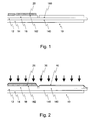
- Fig. 1 and 2 show individual steps of the inventive manufacturing method of a first power semiconductor substrate according to the invention.
- Fig. 3 shows an arrangement with a second power semiconductor substrate according to the invention.
- Fig. 1 and 2 show individual steps of the manufacturing method according to the invention of a first power semiconductor substrate (10) according to the invention.
- Fig. 1 is a power semiconductor substrate (10) based on a known DCB substrate shown.
- This has a ceramic base body (12), with a thickness of 250 .mu.m to 700 .mu.m, made of aluminum oxide, and metallic laminations (14, 16) arranged on the two main surfaces (140, 160) of this base body (12).
- These are designed as copper foils with a thickness between 200 .mu.m and 500 .mu.m.
- the copper foil (14) on the first main surface (140) of the main body (12) is formed flat and serves the thermal contact to a heat sink, not shown.
- the copper foil (16) on the second main surface (160) of the main body (12) is structured in itself and thus forms conductor tracks and also the contact surfaces (162) themselves.
- the interconnects may still have a cover layer in a substantial part of their course.
- the contact surfaces (162) in such embodiments have no cover and can thus be connected to semiconductor devices, connecting or connecting elements.
- a pasty layer (20) is arranged on a contact surface (162) or a part of a conductor track. It is particularly preferred if the layer thickness of this pasty layer is between 10 .mu.m and 200 .mu.m.
- the pasty layer (20) itself consists of a mixture of a metal material in the form of metal flakes with a maximum extension of the order of microns and a solvent.
- the material of the metal flakes is especially silver, but also other precious metals or mixtures with a precious metal content of more than 90 out of 100.
- Fig. 2 shows the pressurization (30) on the pasty layer (20) to form a metallic layer.
- a film (40) for example a Teflon film, which was applied before the pressurization (30).
- a film (40) for example a Teflon film, which was applied before the pressurization (30).
- the maximum final pressure during the pressurization (30) corresponds to at least 8 MPa.
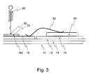
- Fig. 3 shows an arrangement with a second power semiconductor substrate according to the invention (10), a power semiconductor device (50) and a contact spring (60).
- the power semiconductor substrate (10) is again as in FIG Fig. 1 described a DCB substrate.
- a power semiconductor device (50) here a power diode, arranged and connected to the conductor track (16) by soldering, in which case this connection variant is not to be understood as a limitation.
- the power diode (50) is further connected by means of a likewise non-limiting wire bond connection (52) with a second conductor track (16).
- this second conductor track has a thin gold layer (18) with a thickness in the range of a few atomic layers in order to improve the electrical contact to the bonding wire (52).
- a metallic layer (20) arranged according to the method described above.
- This layer (20) is a silver layer and has a thickness of more than 10 ⁇ m. Also suitable are other materials, preferably with a proportion of a noble metal of more than 90 out of 100.
- a contact spring (60) is also shown.
- Their contact foot (62) is in communication with the metallic layer (20) and represents the contact of an outwardly, for example, out of a power semiconductor module, leading connecting element.
- An advantage of the power semiconductor substrate (10) according to the invention is that an excellent contact surface is formed by the thickness of the metallic layer (20) of more than 10 .mu.m, preferably of more than 50 .mu.m in order in combination with pressure-contacted contact springs (60) durable and very high quality train high quality connections.
- the preparation according to the invention corresponds to the state in terms of the required materials, as well as the necessary equipment of a pressure sintered connection of the technique.
- the production of such a power semiconductor substrate (10) is particularly advantageous because simple and inexpensive, possible.
Abstract
Description
- Die Erfindung beschreibt ein Leistungshalbleitersubstrat mit einem isolierenden Grundkörper, mindestens einer Leiterbahn und mindestens einer Kontaktfläche einer dieser Leiterbahnen. Derartige Leistungshalbleitersubstrate sind beispielhaft bekannt als AMD- (active metal braze), DCB- (direct copper bonding) oder IMS- (insulated metal substrat) Substrate.
- Die Kontaktfläche, als Teil oder Abschnitt einer Leiterbahn, dient der elektrisch leitenden Verbindung beispielhaft mit Leistungshalbleiterbauelementen oder mit externen Verbindungselementen. Derartige Verbindungselemente können mit der Kontaktfläche beispielhaft mittels löttechnischer Verbindungen oder mittels druckkontaktierter Verbindungen ausgebildet sein. Speziell bei druckkontaktierten Verbindungen sind hier Verbindungen mit Kontaktfedern von besonderem Interesse.
- Gemäß dem Stand der Technik sind DCB- Substrate bekannt, die aus einem keramischen Grundkörper, häufig Aluminiumoxyd oder Aluminiumnitrid, mit hierauf angeordneten Leiterbahnen aus einer Kupferfolie. Derartige Leiterbahnen sind bevorzugt für löttechnische Verbindungen und bilden hierbei die Kontaktfläche selbst aus. Ebenso ist es bekannt einige oder alle Kontaktflächen mit einer zusätzliche dünnen Goldschicht, vorzugsweise mit einer Dicke von wenigen Atomlagen, auszubilden. Diese ist besonders für Kontaktflächen von Drahtbondverbindungen vorteilhaft. In Verbindung mit druckkontaktierten Anschlusselementen, wie Hilfs- oder Lastanschlusselemente von Leistungshalbleitermodulen, die gemäß dem Stand der Technik als Kontaktfedern ausgebildet sein können, sind diese Kontaktflächen nicht ausreichend. Durch die thermische Belastung, sowie die Druckbeaufschlagung können die Kontaktfüße der Kontaktfedern die dünne Goldschicht beschädigen und somit die Kontaktsicherheit beeinträchtigen.
- Der Erfindung liegt die Aufgabe zugrunde ein Leistungshalbleitersubstrat mit verbesserten Kontakteigenschaften der Kontaktflächen speziell für druckkontaktierte Anwendungen vorzustellen, sowie ein einfaches und kostengünstiges Herstellungsverfahren für ein derartiges Leistungshalbleitersubstrat anzugeben.
- Diese Aufgabe wird erfindungsgemäß gelöst, durch ein Leistungshalbleiterbauelement mit den Merkmale des Anspruchs 1 hergestellt mittels eines Verfahrens nach Anspruch 5. Bevorzugte Ausführungsformen sind in den Unteransprüchen beschrieben.
- Ausgangspunkt der Erfindung ist ein Leistungshalbleitersubstrat mit einem isolierenden flächigen Grundkörper, mindestens einer Leiterbahn und mindestens einer Kontaktfläche als Teil dieser Leiterbahn. Erfindungsgemäß ist hierbei auf dieser Kontaktfläche eine vorzugsweise mindestens 10 Mikrometer dicke Schicht eines Werkstoffs mittels einer Drucksinterverbindung dieses metallischen Werkstoffs angeordnet. Wobei unter Drucksinterverbindung hier verstanden werden sollt, dass eine Schicht eines Werkstoffs mittels des im Weiteren genannten Verfahrens angeordnet wird.
- Hierbei ist es bevorzugt, wenn der zweite metallische Werkstoff einen Anteil von mehr als 90 von 100 eines Edelmetalls aufweist. Besonders bevorzugt ist es hierbei, wenn dieses Edelmetall Silber ist.
- Weiterhin kann es bevorzugt sein zwischen der Kontaktfläche und der metallischen Schicht eine weitere metallische Schicht eines Edelmetalls, vorzugsweise Gold, mit einer Schichtdicke von wenigen Atomlagen anzuordnen.
- Das erfindungsgemäße Verfahren zur Herstellung eines derartigen Leistungshalbleitersubstrats weist folgende wesentliche Schritte auf:
- Herstellung eines Leistungshalbleitersubstrats mit einem flächigen isolierenden Grundkörper, Leiterbahnen und Kontaktflächen dieser Leiterbahnen;
- Anordnung einer pastösen Schicht, aus dem metallischen Werkstoffs und einem Lösungsmittel, auf mindestens einer Kontaktfläche des Leistungshalbleitersubstrats;
- Druckbeaufschlagung auf die pastöse Schicht. Hierbei ist es bevorzugt den überwiegenden Teil des Lösungsmittels vor der Druckbeaufschlagung aus der pastösen Schicht auszutreiben.
- Es kann hierbei bevorzugt sein, wenn die pastöse Schicht mittels eines Schablonendruckverfahrens aufgebracht wird. Hierbei kann einerseits die notwendige Positioniergenauigkeit, bei der geforderten Schichtdicke, erreicht werden. Andererseits ist dieses Verfahren kostengünstig realisierbar.
- Eine vorteilhafte Ausführung der Druckbeaufschlagung auf die pastöse Schicht kann durch die Anwendung einer Presse und zweier Pressstempel gegeben sein. Hierbei ist es zudem bevorzugt, wenn mindestens ein Pressstempel mit einem darauf angeordneten quasihydrostatischen Druck erzeugenden Silikonkissen ausgebildet ist.
- Hierbei ist es ebenfalls bevorzugt auf dem Leistungshalbleitersubstrat einer Folie, vorzugsweise eine Teflonfolie, anzuordnen und anschließend diesen Verbund mit Druck zu beaufschlagen.
- Besonders bevorzugte Weiterbildungen dieses Leistungshalbleitersubstrats sowie des Herstellungsverfahrens sind in der jeweiligen Beschreibung der Ausführungsbeispiele genannt. Die erfinderische Lösung wird zudem an Hand der Ausführungsbeispiele der
Fig. 1 bis 3 weiter erläutert. -
Fig. 1 und 2 zeigen einzelne Schritte des erfindungsgemäßen Herstellungsverfahrens eines ersten erfindungsgemäßen Leistungshalbleitersubstrats. -
Fig. 3 zeigt eine Anordnung mit einem zweiten erfindungsgemäßen Leistungshalbleitersubstrat. -
Fig. 1 und 2 zeigen einzelne Schritte des erfindungsgemäßen Herstellungsverfahrens eines ersten erfindungsgemäßen Leistungshalbleitersubstrats (10). InFig. 1 ist ein Leistungshalbleitersubstrat (10) auf der Grundlage eines bekannten DCB- Substrats dargestellt. Dieses weist einen keramischen Grundkörper (12), mit einer Dicke von 250µm bis 700µm, aus Aluminiumoxyd sowie auf den beiden Hauptflächen (140, 160) dieses Grundkörpers (12) angeordnete metallische Kaschierungen (14, 16) auf. Diese sind als Kupferfolien mit einer Dicke zwischen 200µm und 500µm ausgebildet. Die Kupferfolie (14) auf der ersten Hauptfläche (140) des Grundkörpers (12) ist flächig ausgebildet und dient dem thermischen Kontakt zu einem nicht dargestellten Kühlkörper. Die Kupferfolie (16) auf der zweiten Hauptfläche (160) des Grundkörpers (12) ist in sich strukturiert und bildet somit Leiterbahnen und auch die Kontaktflächen (162) selbst aus. - In anderen bevorzugten Ausgestaltungen können die Leiterbahnen in einem wesentlichen Teil ihres Verlaufs noch eine Abdeckschicht aufweisen. Die Kontaktflächen (162) weisen in derartigen Ausgestaltungen keine Abdeckung auf und können somit mit Halbleiterbauelementen, Verbindungs- oder Anschlusselementen verbunden werden.
- Gemäß dem erfindungsgemäßen Verfahren wird in einem ersten nicht explizit dargestellten Schritt, vorzugsweise mittels Schablonendrucktechnik, eine pastöse Schicht (20), wie sie aus Sinterverbindungen nach dem Stand der Technik bekannt ist, auf einer Kontaktfläche (162) oder einem Teil einer Leiterbahn angeordnet. Hierbei ist es besonders bevorzugt, wenn die Schichtdicke dieser pastösen Schicht zwischen 10µm und 200µm beträgt.
- Die pastöse Schicht (20) selbst besteht aus einer Mischung eines metallischen Werkstoffs in Form von Metallflocken mit einer maximalen Ausdehnung in der Größenordnung von Mikrometern und einem Lösungsmittel. Als Material der Metallflocken eignet sich besonders Silber, aber auch andere Edelmetalle oder Mischungen mit einem Edelmetallanteil von mehr als 90 von 100.
-
Fig. 2 zeigt die Druckbeaufschlagung (30) auf die pastöse Schicht (20) zur Ausbildung einer metallischen Schicht. Vor dieser Druckbeaufschlagung (30) ist es vorteilhaft das Lösungsmittel zu mindestens 95 von 100 aus der pastösen Schicht (20) auszutreiben. Dies wird bevorzugt mittels Temperaturbeaufschlagung auf das Leistungshalbleitersubstrat (10) erreicht. Diese Erwärmung auf mindestens 350K wird auch während der anschließenden Druckbeaufschlagung (30) beibehalten oder noch erhöht. - Zusätzlich dargestellt und auch bevorzugt ist hier eine Folie (40), beispielhaft eine Teflonfolie, die vor der Druckbeaufschlagung (30) aufgebracht wurde. Hierbei ist es bevorzugt das gesamte Leistungshalbleitersubstrat (10) abzudecken. Es ist allerdings in manchen Ausbildungen möglich selektiv nur die jeweilige pastöse Schicht (20) mit der Folie (30) zu bedecken.
- Um eine ausreichend haftende Verbindung zwischen der pastösen Schicht (20) und der Kontaktfläche (162) auszubilden ist es bevorzugt, wenn der maximale Enddruck bei der Druckbeaufschlagung (30) mindestens 8MPa entspricht.
-
Fig. 3 zeigt eine Anordnung mit einem zweiten erfindungsgemäßen Leistungshalbleitersubstrat (10), einem Leistungshalbleiterbauelement (50) und einer Kontaktfeder (60). Das Leistungshalbleitersubstrat (10) ist wiederum wie inFig. 1 beschrieben ein DCB- Substrat. Auf einer Leiterbahn (16) dieses Substrats ist ein Leistungshalbleiterbauelement (50), hier eine Leistungsdiode, angeordnet und mit der Leiterbahn (16) löttechnisch verbunden, wobei hier diese Verbindungsvariante nicht als Beschränkung zu verstehen ist. - Die Leistungsdiode (50) ist weiterhin mittels einer ebenfalls nicht einschränkenden Drahtbondverbindung (52) mit einer zweiten Leiterbahn (16) verbunden. Diese zweite Leiterbahn weist im Bereich der Kontaktfläche (162) eine dünne Goldschicht (18) mit einer Dicke im Bereich einiger Atomlagen auf um den elektrischen Kontakt zum Bonddraht (52) zu verbessern. Auf der Goldschicht (18) ist erfindungsgemäß eine metallische Schicht (20), nach dem oben beschriebenen Verfahren angeordnet. Diese Schicht (20) ist eine Silberschicht und weist ein Dicke von mehr als 10µm auf. Ebenso geeignet sind andere Werkstoffe, vorzugsweise mit einem Anteil eines Edelmetalls von mehr als 90 von 100.
- Ebenfalls dargestellt ist eine Kontaktfeder (60), wie sie für druckkontaktierte Anschlusselemente bekannte ist. Deren Kontaktfuß (62) ist mit der metallischen Schicht (20) in Verbindung und stellte den Kontakt eines nach außen, beispielhaft aus einem Leistungshalbleitermodul heraus, führenden Anschlusselements dar.
- Ein Vorteil des erfindungsgemäßen Leistungshalbleitersubstrats (10) ist es, dass durch die Dicke der metallischen Schicht (20) von mehr als 10µm, vorzugsweise von mehr als 50µm eine hervorragende Kontaktfläche ausgebildet wird, um in Kombination mit druckkontaktierten Kontaktfedern (60) dauerhafte und qualitativ sehr hochwertige Verbindungen auszubilden.
- Die erfindungsgemäße Herstellung entspricht hinsichtlich der benötigten Materialien, wie auch der notwendigen Anlagen einer Drucksinterverbindung dem Stand der Technik. Hierdurch ist die Herstellung eines derartigen Leistungshalbleitersubstrats (10) besonders vorteilhaft, weil einfach und kostengünstig, möglich.
Claims (10)
- Leistungshalbleitersubstrat (10) mit einem isolierenden flächigen Grundkörper (12), mindestens einer Leiterbahn (16) und mindestens einer Kontaktfläche (162) als Teil dieser Leiterbahn (16), wobei auf dieser Kontaktfläche (162) eine Schicht (20) eines Werkstoffs mittels einer Drucksinterverbindung dieses metallischen Werkstoffs angeordnet ist.
- Leistungshalbleiterbauelement nach Anspruch 1,
wobei der metallische Werkstoffs eine Schichtdicke von mindestens 10 Mikrometern und einen Anteil von mehr als 90 von 100 eines Edelmetalls aufweist. - Leistungshalbleiterbauelement nach Anspruch 2,
wobei das Edelmetall Silber ist. - Leistungshalbleiterbauelement nach Anspruch 1,
wobei zwischen der Kontaktfläche (162) und der metallischen Schicht (20) eine weitere metallische Schicht (18) eines Edelmetalls mit einer Schichtdicke von wenigen Atomlagen angeordnet ist. - Verfahren zur Herstellung eines Leistungshalbleitersubstrats (10) nach Anspruch 1 mit den wesentlichen Schritten:• Herstellung eines Leistungshalbleitersubstrats mit einem flächigen isolierenden Grundkörper (12), Leiterbahnen (16) und Kontaktflächen (162) als Teil dieser Leiterbahnen (16);• Anordnung einer pastösen Schicht (20), aus einem metallischen Werkstoffs und einem Lösungsmittel, auf mindestens einer Kontaktfläche (162) des Leistungshalbleitersubstrats (10);• Druckbeaufschlagung (30) auf die pastöse Schicht (20).
- Verfahren nach Anspruch 5,
wobei die pastöse Schicht (20) mittels eines Schablonendruckverfahrens aufgebracht wird. - Verfahren nach Anspruch 5,
wobei der Druck (30) mittels einer Presse und zweier Pressstempel, wobei mindestens ein Pressstempel mit einem darauf angeordneten quasihydrostatischen Druck erzeugendes Silikonkissen ausgebildet ist, aufgebracht wird. - Verfahren nach Anspruch 5,
wobei der maximale Enddruck bei der Druckbeaufschlagung (30) mindestens 8MPa entspricht. - Verfahren nach Anspruch 5,
wobei während der Druckbeaufschlagung (30) das Leistungshalbleitersubstrat (10) auf mehr als 350K erwärmt ist. - Verfahren nach Anspruch 5,
wobei vor der Druckbeaufschlagung (30) das Leistungshalbleitersubstrat (10) mit einer Folie (40) bedeckt wird.
Applications Claiming Priority (1)
| Application Number | Priority Date | Filing Date | Title |
|---|---|---|---|
| DE102007022336A DE102007022336A1 (de) | 2007-05-12 | 2007-05-12 | Leistungshalbleitersubstrat mit Metallkontaktschicht sowie Herstellungsverfahren hierzu |
Publications (3)
| Publication Number | Publication Date |
|---|---|
| EP1993132A2 true EP1993132A2 (de) | 2008-11-19 |
| EP1993132A3 EP1993132A3 (de) | 2010-09-08 |
| EP1993132B1 EP1993132B1 (de) | 2018-07-11 |
Family
ID=39642636
Family Applications (1)
| Application Number | Title | Priority Date | Filing Date |
|---|---|---|---|
| EP08008713.3A Active EP1993132B1 (de) | 2007-05-12 | 2008-05-09 | Leistungshalbleitersubstrat mit Metallkontaktschicht sowie Herstellungsverfahren hierzu |
Country Status (5)
| Country | Link |
|---|---|
| US (1) | US9768036B2 (de) |
| EP (1) | EP1993132B1 (de) |
| JP (1) | JP5119039B2 (de) |
| CN (1) | CN101304012B (de) |
| DE (1) | DE102007022336A1 (de) |
Cited By (2)
| Publication number | Priority date | Publication date | Assignee | Title |
|---|---|---|---|---|
| WO2016184645A1 (en) * | 2015-05-18 | 2016-11-24 | Danfoss Silicon Power Gmbh | Method for manufacturing a circuit carrier |
| EP3305043A4 (de) * | 2015-05-26 | 2019-02-20 | Stora Enso Oyj | Verfahren und anordnung zur herstellung von elektrisch leitfähigen mustern auf substraten |
Families Citing this family (3)
| Publication number | Priority date | Publication date | Assignee | Title |
|---|---|---|---|---|
| WO2013159035A2 (en) * | 2012-04-19 | 2013-10-24 | Medical College Of Wisconsin, Inc. | Highly sensitive surveillance using detection of cell free dna |
| JP6812424B2 (ja) | 2016-05-18 | 2021-01-13 | テルモ株式会社 | 血液検査システムおよび血液検査システムの制御方法 |
| DE102022213183B3 (de) | 2022-12-07 | 2024-01-18 | Zf Friedrichshafen Ag | Verfahren zum bilden eines leistungsmoduls |
Citations (2)
| Publication number | Priority date | Publication date | Assignee | Title |
|---|---|---|---|---|
| DE4233073A1 (de) | 1992-10-01 | 1994-04-07 | Siemens Ag | Verfahren zum Herstellen eines Halbleiter-Modulaufbaus |
| US5807626A (en) | 1995-07-21 | 1998-09-15 | Kabushiki Kaisha Toshiba | Ceramic circuit board |
Family Cites Families (14)
| Publication number | Priority date | Publication date | Assignee | Title |
|---|---|---|---|---|
| DE3414065A1 (de) * | 1984-04-13 | 1985-12-12 | Siemens AG, 1000 Berlin und 8000 München | Anordnung bestehend aus mindestens einem auf einem substrat befestigten elektronischen bauelement und verfahren zur herstellung einer derartigen anordnung |
| IN168174B (de) * | 1986-04-22 | 1991-02-16 | Siemens Ag | |
| EP0330896A3 (de) * | 1988-03-03 | 1991-01-09 | Siemens Aktiengesellschaft | Verfahren zum Befestigen von Halbleiterbauelementen auf Substraten und Anordnungen zur Durchführung desselben |
| DE19646369B4 (de) * | 1996-11-09 | 2008-07-31 | Robert Bosch Gmbh | Keramische Mehrlagenschaltung und Verfahren zu ihrer Herstellung |
| US6228196B1 (en) * | 1998-06-05 | 2001-05-08 | Murata Manufacturing Co., Ltd. | Method of producing a multi-layer ceramic substrate |
| JP3322305B2 (ja) * | 1999-02-25 | 2002-09-09 | 日本電気株式会社 | 半導体装置の製造方法 |
| JP3656484B2 (ja) * | 1999-03-03 | 2005-06-08 | 株式会社村田製作所 | セラミック多層基板の製造方法 |
| DE10062108B4 (de) * | 2000-12-13 | 2010-04-15 | Infineon Technologies Ag | Leistungsmodul mit verbessertem transienten Wärmewiderstand |
| JP2003101184A (ja) * | 2001-09-27 | 2003-04-04 | Kyocera Corp | セラミック回路基板およびその製造方法 |
| DE10316355C5 (de) * | 2003-04-10 | 2008-03-06 | Semikron Elektronik Gmbh & Co. Kg | Leistungshalbeitermodul mit flexibler äusserer Anschlussbelegung |
| US20070183920A1 (en) * | 2005-02-14 | 2007-08-09 | Guo-Quan Lu | Nanoscale metal paste for interconnect and method of use |
| DE102004019567B3 (de) * | 2004-04-22 | 2006-01-12 | Semikron Elektronik Gmbh & Co. Kg | Verfahren zur Befestigung von elektronischen Bauelementen auf einem Substrat |
| DE102005047567B3 (de) * | 2005-10-05 | 2007-03-29 | Semikron Elektronik Gmbh & Co. Kg | Leistungshalbleitermodul mit Isolationszwischenlage und Verfahren zu seiner Herstellung |
| DE102005047566C5 (de) * | 2005-10-05 | 2011-06-09 | Semikron Elektronik Gmbh & Co. Kg | Anordnung mit einem Leistungshalbleiterbauelement und mit einem Gehäuse sowie Herstellungsverfahren hierzu |
-
2007
- 2007-05-12 DE DE102007022336A patent/DE102007022336A1/de not_active Withdrawn
-
2008
- 2008-05-08 JP JP2008122169A patent/JP5119039B2/ja not_active Expired - Fee Related
- 2008-05-09 EP EP08008713.3A patent/EP1993132B1/de active Active
- 2008-05-09 CN CN2008100967353A patent/CN101304012B/zh active Active
- 2008-05-12 US US12/152,021 patent/US9768036B2/en not_active Expired - Fee Related
Patent Citations (2)
| Publication number | Priority date | Publication date | Assignee | Title |
|---|---|---|---|---|
| DE4233073A1 (de) | 1992-10-01 | 1994-04-07 | Siemens Ag | Verfahren zum Herstellen eines Halbleiter-Modulaufbaus |
| US5807626A (en) | 1995-07-21 | 1998-09-15 | Kabushiki Kaisha Toshiba | Ceramic circuit board |
Cited By (4)
| Publication number | Priority date | Publication date | Assignee | Title |
|---|---|---|---|---|
| WO2016184645A1 (en) * | 2015-05-18 | 2016-11-24 | Danfoss Silicon Power Gmbh | Method for manufacturing a circuit carrier |
| CN107667419A (zh) * | 2015-05-18 | 2018-02-06 | 丹佛斯硅动力有限责任公司 | 用于制造电路载体的方法 |
| EP3305043A4 (de) * | 2015-05-26 | 2019-02-20 | Stora Enso Oyj | Verfahren und anordnung zur herstellung von elektrisch leitfähigen mustern auf substraten |
| US10887998B2 (en) | 2015-05-26 | 2021-01-05 | Stora Enso Oyj | Method and an arrangement for producing electrically conductive patterns on substrates |
Also Published As
| Publication number | Publication date |
|---|---|
| EP1993132B1 (de) | 2018-07-11 |
| EP1993132A3 (de) | 2010-09-08 |
| CN101304012A (zh) | 2008-11-12 |
| US20090008784A1 (en) | 2009-01-08 |
| JP2008283183A (ja) | 2008-11-20 |
| DE102007022336A1 (de) | 2008-11-20 |
| CN101304012B (zh) | 2013-03-13 |
| JP5119039B2 (ja) | 2013-01-16 |
| US9768036B2 (en) | 2017-09-19 |
Similar Documents
| Publication | Publication Date | Title |
|---|---|---|
| EP1993133B1 (de) | Verfahren zur Herstellung eines gesinterten Leistungshalbleitersubstrates | |
| EP1956647B1 (de) | Schaltungsanordnung mit Verbindungseinrichtung sowie Herstellungsverfahren hierzu | |
| DE102005047566C5 (de) | Anordnung mit einem Leistungshalbleiterbauelement und mit einem Gehäuse sowie Herstellungsverfahren hierzu | |
| DE102010044709B4 (de) | Leistungshalbleitermodul mit Metallsinterverbindungen sowie Herstellungsverfahren | |
| DE102012105840B4 (de) | Verfahren zum Befestigen einer Metallfläche auf einen Träger und Verfahren zum Befestigen eines Chips auf einen Chipträger | |
| DE102010021765B4 (de) | Herstellungsverfahren zur Anordnung zweier Verbindungspartner mittels einer Niedertemperatur Drucksinterverbindung | |
| DE102010021764B4 (de) | Verfahren zur Niedertemperatur Drucksinterverbindung zweier Verbindungspartner | |
| DE102007054710B3 (de) | Verfahren zur Herstellung einer Halbleiterbaugruppe | |
| DE102012222791A1 (de) | Verfahren zur Kontaktierung eines Halbleiters und Halbleiterbauelement mit erhöhter Stabilität gegenüber thermomechanischen Einflüssen | |
| EP1993132B1 (de) | Leistungshalbleitersubstrat mit Metallkontaktschicht sowie Herstellungsverfahren hierzu | |
| DE102008055138A1 (de) | Hochtemperaturbeständige lötmittelfreie Bauelementstruktur und Verfahren zum elektrischen Kontaktieren | |
| EP3555913B1 (de) | Halbleitermodul mit bodenplatte mit hohlwölbung | |
| DE102009024371A1 (de) | Verfahren zur Herstellung einer Stromrichteranordnung mit Kühleinrichtung und Stromrichteranordnung | |
| DE102008034946A1 (de) | Edelmetallverbindungsmittel sowie Herstellungs- und Verwendungsverfahren hierzu | |
| DE102014203306A1 (de) | Herstellen eines Elektronikmoduls | |
| DE102011083423A1 (de) | Kontaktfederanordnung und Verfahren zur Herstellung derselben | |
| EP2498283A2 (de) | Verfahren zur Herstellung eines Leistungshalbleitersubstrates | |
| DE102007022338B4 (de) | Herstellungsverfahren für ein Leistungshalbleiterbauelement mit Metallkontaktschicht | |
| DE102009016112A1 (de) | Einrichtung mit einem elektrischen Bauelement und wenigstens einer elektrischen Anschlussleitung | |
| DE102008033410B4 (de) | Leistungselektronische Verbindungseinrichtung mit einem Leistungshalbleiterbauelement und Herstellungsverfahren hierzu | |
| DE102015107712B3 (de) | Verfahren zur Herstellung eines Schaltungsträgers | |
| DE102013102637A1 (de) | Metall-Keramik-Substrat sowie Verfahren zum Herstellen eines Metall-Keramik-Substrates | |
| DE102008034952B4 (de) | Edelmetallverbindungsmittel und Verwendungsverfahren hierzu | |
| DE102012222012A1 (de) | Leistungshalbleitereinrichtung und ein Verfahren zur Herstellung einer Leistungshalbleitereinrichtung | |
| EP2148363A2 (de) | Edelmetall basiertes Verbindungsmittel mit einem Feststoffanteil und einem Flüssiganteil und Verwendungsverfahren hierzu |
Legal Events
| Date | Code | Title | Description |
|---|---|---|---|
| PUAI | Public reference made under article 153(3) epc to a published international application that has entered the european phase |
Free format text: ORIGINAL CODE: 0009012 |
|
| AK | Designated contracting states |
Kind code of ref document: A2 Designated state(s): AT BE BG CH CY CZ DE DK EE ES FI FR GB GR HR HU IE IS IT LI LT LU LV MC MT NL NO PL PT RO SE SI SK TR |
|
| AX | Request for extension of the european patent |
Extension state: AL BA MK RS |
|
| PUAL | Search report despatched |
Free format text: ORIGINAL CODE: 0009013 |
|
| AK | Designated contracting states |
Kind code of ref document: A3 Designated state(s): AT BE BG CH CY CZ DE DK EE ES FI FR GB GR HR HU IE IS IT LI LT LU LV MC MT NL NO PL PT RO SE SI SK TR |
|
| AX | Request for extension of the european patent |
Extension state: AL BA MK RS |
|
| 17P | Request for examination filed |
Effective date: 20100812 |
|
| AKX | Designation fees paid |
Designated state(s): AT BE BG CH CY CZ DE DK EE ES FI FR GB GR HR HU IE IS IT LI LT LU LV MC MT NL NO PL PT RO SE SI SK TR |
|
| 17Q | First examination report despatched |
Effective date: 20110610 |
|
| STAA | Information on the status of an ep patent application or granted ep patent |
Free format text: STATUS: EXAMINATION IS IN PROGRESS |
|
| REG | Reference to a national code |
Ref country code: DE Ref legal event code: R079 Ref document number: 502008016169 Country of ref document: DE Free format text: PREVIOUS MAIN CLASS: H01L0023373000 Ipc: H01L0023498000 |
|
| RIC1 | Information provided on ipc code assigned before grant |
Ipc: H01L 23/00 20060101ALI20180118BHEP Ipc: H01L 21/48 20060101ALI20180118BHEP Ipc: H05K 3/24 20060101ALI20180118BHEP Ipc: C04B 37/02 20060101ALI20180118BHEP Ipc: H05K 3/06 20060101ALI20180118BHEP Ipc: H01L 25/07 20060101ALI20180118BHEP Ipc: H05K 3/12 20060101ALI20180118BHEP Ipc: H01L 23/373 20060101ALI20180118BHEP Ipc: H05K 1/03 20060101ALI20180118BHEP Ipc: C04B 35/645 20060101ALI20180118BHEP Ipc: H01L 23/498 20060101AFI20180118BHEP |
|
| GRAP | Despatch of communication of intention to grant a patent |
Free format text: ORIGINAL CODE: EPIDOSNIGR1 |
|
| STAA | Information on the status of an ep patent application or granted ep patent |
Free format text: STATUS: GRANT OF PATENT IS INTENDED |
|
| INTG | Intention to grant announced |
Effective date: 20180307 |
|
| GRAS | Grant fee paid |
Free format text: ORIGINAL CODE: EPIDOSNIGR3 |
|
| GRAA | (expected) grant |
Free format text: ORIGINAL CODE: 0009210 |
|
| STAA | Information on the status of an ep patent application or granted ep patent |
Free format text: STATUS: THE PATENT HAS BEEN GRANTED |
|
| AK | Designated contracting states |
Kind code of ref document: B1 Designated state(s): AT BE BG CH CY CZ DE DK EE ES FI FR GB GR HR HU IE IS IT LI LT LU LV MC MT NL NO PL PT RO SE SI SK TR |
|
| REG | Reference to a national code |
Ref country code: GB Ref legal event code: FG4D Free format text: NOT ENGLISH |
|
| REG | Reference to a national code |
Ref country code: CH Ref legal event code: EP |
|
| REG | Reference to a national code |
Ref country code: AT Ref legal event code: REF Ref document number: 1017799 Country of ref document: AT Kind code of ref document: T Effective date: 20180715 |
|
| REG | Reference to a national code |
Ref country code: IE Ref legal event code: FG4D Free format text: LANGUAGE OF EP DOCUMENT: GERMAN |
|
| REG | Reference to a national code |
Ref country code: DE Ref legal event code: R096 Ref document number: 502008016169 Country of ref document: DE |
|
| REG | Reference to a national code |
Ref country code: NL Ref legal event code: MP Effective date: 20180711 |
|
| REG | Reference to a national code |
Ref country code: LT Ref legal event code: MG4D |
|
| PG25 | Lapsed in a contracting state [announced via postgrant information from national office to epo] |
Ref country code: NL Free format text: LAPSE BECAUSE OF FAILURE TO SUBMIT A TRANSLATION OF THE DESCRIPTION OR TO PAY THE FEE WITHIN THE PRESCRIBED TIME-LIMIT Effective date: 20180711 |
|
| PG25 | Lapsed in a contracting state [announced via postgrant information from national office to epo] |
Ref country code: FI Free format text: LAPSE BECAUSE OF FAILURE TO SUBMIT A TRANSLATION OF THE DESCRIPTION OR TO PAY THE FEE WITHIN THE PRESCRIBED TIME-LIMIT Effective date: 20180711 Ref country code: PL Free format text: LAPSE BECAUSE OF FAILURE TO SUBMIT A TRANSLATION OF THE DESCRIPTION OR TO PAY THE FEE WITHIN THE PRESCRIBED TIME-LIMIT Effective date: 20180711 Ref country code: BG Free format text: LAPSE BECAUSE OF FAILURE TO SUBMIT A TRANSLATION OF THE DESCRIPTION OR TO PAY THE FEE WITHIN THE PRESCRIBED TIME-LIMIT Effective date: 20181011 Ref country code: SE Free format text: LAPSE BECAUSE OF FAILURE TO SUBMIT A TRANSLATION OF THE DESCRIPTION OR TO PAY THE FEE WITHIN THE PRESCRIBED TIME-LIMIT Effective date: 20180711 Ref country code: GR Free format text: LAPSE BECAUSE OF FAILURE TO SUBMIT A TRANSLATION OF THE DESCRIPTION OR TO PAY THE FEE WITHIN THE PRESCRIBED TIME-LIMIT Effective date: 20181012 Ref country code: LT Free format text: LAPSE BECAUSE OF FAILURE TO SUBMIT A TRANSLATION OF THE DESCRIPTION OR TO PAY THE FEE WITHIN THE PRESCRIBED TIME-LIMIT Effective date: 20180711 Ref country code: NO Free format text: LAPSE BECAUSE OF FAILURE TO SUBMIT A TRANSLATION OF THE DESCRIPTION OR TO PAY THE FEE WITHIN THE PRESCRIBED TIME-LIMIT Effective date: 20181011 Ref country code: IS Free format text: LAPSE BECAUSE OF FAILURE TO SUBMIT A TRANSLATION OF THE DESCRIPTION OR TO PAY THE FEE WITHIN THE PRESCRIBED TIME-LIMIT Effective date: 20181111 |
|
| PG25 | Lapsed in a contracting state [announced via postgrant information from national office to epo] |
Ref country code: ES Free format text: LAPSE BECAUSE OF FAILURE TO SUBMIT A TRANSLATION OF THE DESCRIPTION OR TO PAY THE FEE WITHIN THE PRESCRIBED TIME-LIMIT Effective date: 20180711 Ref country code: LV Free format text: LAPSE BECAUSE OF FAILURE TO SUBMIT A TRANSLATION OF THE DESCRIPTION OR TO PAY THE FEE WITHIN THE PRESCRIBED TIME-LIMIT Effective date: 20180711 Ref country code: HR Free format text: LAPSE BECAUSE OF FAILURE TO SUBMIT A TRANSLATION OF THE DESCRIPTION OR TO PAY THE FEE WITHIN THE PRESCRIBED TIME-LIMIT Effective date: 20180711 |
|
| REG | Reference to a national code |
Ref country code: DE Ref legal event code: R097 Ref document number: 502008016169 Country of ref document: DE |
|
| PG25 | Lapsed in a contracting state [announced via postgrant information from national office to epo] |
Ref country code: EE Free format text: LAPSE BECAUSE OF FAILURE TO SUBMIT A TRANSLATION OF THE DESCRIPTION OR TO PAY THE FEE WITHIN THE PRESCRIBED TIME-LIMIT Effective date: 20180711 Ref country code: CZ Free format text: LAPSE BECAUSE OF FAILURE TO SUBMIT A TRANSLATION OF THE DESCRIPTION OR TO PAY THE FEE WITHIN THE PRESCRIBED TIME-LIMIT Effective date: 20180711 Ref country code: RO Free format text: LAPSE BECAUSE OF FAILURE TO SUBMIT A TRANSLATION OF THE DESCRIPTION OR TO PAY THE FEE WITHIN THE PRESCRIBED TIME-LIMIT Effective date: 20180711 Ref country code: IT Free format text: LAPSE BECAUSE OF FAILURE TO SUBMIT A TRANSLATION OF THE DESCRIPTION OR TO PAY THE FEE WITHIN THE PRESCRIBED TIME-LIMIT Effective date: 20180711 |
|
| PLBE | No opposition filed within time limit |
Free format text: ORIGINAL CODE: 0009261 |
|
| STAA | Information on the status of an ep patent application or granted ep patent |
Free format text: STATUS: NO OPPOSITION FILED WITHIN TIME LIMIT |
|
| PG25 | Lapsed in a contracting state [announced via postgrant information from national office to epo] |
Ref country code: DK Free format text: LAPSE BECAUSE OF FAILURE TO SUBMIT A TRANSLATION OF THE DESCRIPTION OR TO PAY THE FEE WITHIN THE PRESCRIBED TIME-LIMIT Effective date: 20180711 Ref country code: SK Free format text: LAPSE BECAUSE OF FAILURE TO SUBMIT A TRANSLATION OF THE DESCRIPTION OR TO PAY THE FEE WITHIN THE PRESCRIBED TIME-LIMIT Effective date: 20180711 |
|
| 26N | No opposition filed |
Effective date: 20190412 |
|
| PG25 | Lapsed in a contracting state [announced via postgrant information from national office to epo] |
Ref country code: SI Free format text: LAPSE BECAUSE OF FAILURE TO SUBMIT A TRANSLATION OF THE DESCRIPTION OR TO PAY THE FEE WITHIN THE PRESCRIBED TIME-LIMIT Effective date: 20180711 |
|
| REG | Reference to a national code |
Ref country code: CH Ref legal event code: PL |
|
| GBPC | Gb: european patent ceased through non-payment of renewal fee |
Effective date: 20190509 |
|
| PG25 | Lapsed in a contracting state [announced via postgrant information from national office to epo] |
Ref country code: CH Free format text: LAPSE BECAUSE OF NON-PAYMENT OF DUE FEES Effective date: 20190531 Ref country code: LI Free format text: LAPSE BECAUSE OF NON-PAYMENT OF DUE FEES Effective date: 20190531 Ref country code: MC Free format text: LAPSE BECAUSE OF FAILURE TO SUBMIT A TRANSLATION OF THE DESCRIPTION OR TO PAY THE FEE WITHIN THE PRESCRIBED TIME-LIMIT Effective date: 20180711 |
|
| REG | Reference to a national code |
Ref country code: BE Ref legal event code: MM Effective date: 20190531 |
|
| PG25 | Lapsed in a contracting state [announced via postgrant information from national office to epo] |
Ref country code: LU Free format text: LAPSE BECAUSE OF NON-PAYMENT OF DUE FEES Effective date: 20190509 |
|
| PG25 | Lapsed in a contracting state [announced via postgrant information from national office to epo] |
Ref country code: TR Free format text: LAPSE BECAUSE OF FAILURE TO SUBMIT A TRANSLATION OF THE DESCRIPTION OR TO PAY THE FEE WITHIN THE PRESCRIBED TIME-LIMIT Effective date: 20180711 |
|
| PG25 | Lapsed in a contracting state [announced via postgrant information from national office to epo] |
Ref country code: IE Free format text: LAPSE BECAUSE OF NON-PAYMENT OF DUE FEES Effective date: 20190509 Ref country code: GB Free format text: LAPSE BECAUSE OF NON-PAYMENT OF DUE FEES Effective date: 20190509 |
|
| PG25 | Lapsed in a contracting state [announced via postgrant information from national office to epo] |
Ref country code: BE Free format text: LAPSE BECAUSE OF NON-PAYMENT OF DUE FEES Effective date: 20190531 |
|
| PG25 | Lapsed in a contracting state [announced via postgrant information from national office to epo] |
Ref country code: PT Free format text: LAPSE BECAUSE OF FAILURE TO SUBMIT A TRANSLATION OF THE DESCRIPTION OR TO PAY THE FEE WITHIN THE PRESCRIBED TIME-LIMIT Effective date: 20181111 Ref country code: FR Free format text: LAPSE BECAUSE OF NON-PAYMENT OF DUE FEES Effective date: 20190531 |
|
| REG | Reference to a national code |
Ref country code: AT Ref legal event code: MM01 Ref document number: 1017799 Country of ref document: AT Kind code of ref document: T Effective date: 20190509 |
|
| PG25 | Lapsed in a contracting state [announced via postgrant information from national office to epo] |
Ref country code: AT Free format text: LAPSE BECAUSE OF NON-PAYMENT OF DUE FEES Effective date: 20190509 |
|
| PG25 | Lapsed in a contracting state [announced via postgrant information from national office to epo] |
Ref country code: CY Free format text: LAPSE BECAUSE OF FAILURE TO SUBMIT A TRANSLATION OF THE DESCRIPTION OR TO PAY THE FEE WITHIN THE PRESCRIBED TIME-LIMIT Effective date: 20180711 |
|
| PG25 | Lapsed in a contracting state [announced via postgrant information from national office to epo] |
Ref country code: HU Free format text: LAPSE BECAUSE OF FAILURE TO SUBMIT A TRANSLATION OF THE DESCRIPTION OR TO PAY THE FEE WITHIN THE PRESCRIBED TIME-LIMIT; INVALID AB INITIO Effective date: 20080509 Ref country code: MT Free format text: LAPSE BECAUSE OF FAILURE TO SUBMIT A TRANSLATION OF THE DESCRIPTION OR TO PAY THE FEE WITHIN THE PRESCRIBED TIME-LIMIT Effective date: 20180711 |
|
| PGFP | Annual fee paid to national office [announced via postgrant information from national office to epo] |
Ref country code: DE Payment date: 20230531 Year of fee payment: 16 |