EP1955404B1 - Procédé de fabrication de corps creux pour des résonateurs - Google Patents
Procédé de fabrication de corps creux pour des résonateurs Download PDFInfo
- Publication number
- EP1955404B1 EP1955404B1 EP06818910A EP06818910A EP1955404B1 EP 1955404 B1 EP1955404 B1 EP 1955404B1 EP 06818910 A EP06818910 A EP 06818910A EP 06818910 A EP06818910 A EP 06818910A EP 1955404 B1 EP1955404 B1 EP 1955404B1
- Authority
- EP
- European Patent Office
- Prior art keywords
- joining
- discs
- faces
- cells
- substrate
- Prior art date
- Legal status (The legal status is an assumption and is not a legal conclusion. Google has not performed a legal analysis and makes no representation as to the accuracy of the status listed.)
- Active
Links
- 238000004519 manufacturing process Methods 0.000 title claims abstract description 9
- 238000000034 method Methods 0.000 claims abstract description 48
- 238000005304 joining Methods 0.000 claims abstract description 39
- 239000000758 substrate Substances 0.000 claims abstract description 23
- 238000005520 cutting process Methods 0.000 claims abstract description 10
- 239000000463 material Substances 0.000 claims description 33
- 229910052758 niobium Inorganic materials 0.000 claims description 17
- 239000010955 niobium Substances 0.000 claims description 17
- GUCVJGMIXFAOAE-UHFFFAOYSA-N niobium atom Chemical compound [Nb] GUCVJGMIXFAOAE-UHFFFAOYSA-N 0.000 claims description 17
- 238000010438 heat treatment Methods 0.000 claims description 16
- 239000013078 crystal Substances 0.000 claims description 12
- 238000003825 pressing Methods 0.000 claims description 8
- 238000005096 rolling process Methods 0.000 claims description 5
- 238000010894 electron beam technology Methods 0.000 claims description 4
- 238000003466 welding Methods 0.000 claims description 4
- 238000007493 shaping process Methods 0.000 claims 4
- 238000007669 thermal treatment Methods 0.000 claims 2
- 235000012431 wafers Nutrition 0.000 abstract 3
- 239000002245 particle Substances 0.000 description 8
- 239000000126 substance Substances 0.000 description 8
- 229910052739 hydrogen Inorganic materials 0.000 description 5
- 230000007547 defect Effects 0.000 description 4
- 230000005684 electric field Effects 0.000 description 4
- 239000001257 hydrogen Substances 0.000 description 4
- 230000000149 penetrating effect Effects 0.000 description 4
- 238000005554 pickling Methods 0.000 description 4
- 235000019592 roughness Nutrition 0.000 description 4
- 239000002887 superconductor Substances 0.000 description 4
- 239000002344 surface layer Substances 0.000 description 4
- UFHFLCQGNIYNRP-UHFFFAOYSA-N Hydrogen Chemical compound [H][H] UFHFLCQGNIYNRP-UHFFFAOYSA-N 0.000 description 3
- 238000001311 chemical methods and process Methods 0.000 description 3
- 239000012535 impurity Substances 0.000 description 3
- 239000002184 metal Substances 0.000 description 3
- 229910052751 metal Inorganic materials 0.000 description 3
- 239000000203 mixture Substances 0.000 description 3
- 230000000694 effects Effects 0.000 description 2
- 239000007789 gas Substances 0.000 description 2
- 238000000926 separation method Methods 0.000 description 2
- 230000009466 transformation Effects 0.000 description 2
- 238000000844 transformation Methods 0.000 description 2
- RYGMFSIKBFXOCR-UHFFFAOYSA-N Copper Chemical compound [Cu] RYGMFSIKBFXOCR-UHFFFAOYSA-N 0.000 description 1
- 240000006829 Ficus sundaica Species 0.000 description 1
- 230000001133 acceleration Effects 0.000 description 1
- 239000002253 acid Substances 0.000 description 1
- 239000002131 composite material Substances 0.000 description 1
- 239000000356 contaminant Substances 0.000 description 1
- 229910052802 copper Inorganic materials 0.000 description 1
- 239000010949 copper Substances 0.000 description 1
- 239000002178 crystalline material Substances 0.000 description 1
- 230000001419 dependent effect Effects 0.000 description 1
- 238000004049 embossing Methods 0.000 description 1
- 230000007613 environmental effect Effects 0.000 description 1
- 230000003628 erosive effect Effects 0.000 description 1
- 238000002474 experimental method Methods 0.000 description 1
- 150000002431 hydrogen Chemical group 0.000 description 1
- 239000003550 marker Substances 0.000 description 1
- 230000013011 mating Effects 0.000 description 1
- 150000002739 metals Chemical class 0.000 description 1
- 230000006911 nucleation Effects 0.000 description 1
- 238000010899 nucleation Methods 0.000 description 1
- 230000002093 peripheral effect Effects 0.000 description 1
- 238000005498 polishing Methods 0.000 description 1
- 238000002360 preparation method Methods 0.000 description 1
- 239000002994 raw material Substances 0.000 description 1
- 230000000717 retained effect Effects 0.000 description 1
- 238000007788 roughening Methods 0.000 description 1
- 230000035945 sensitivity Effects 0.000 description 1
- 238000009987 spinning Methods 0.000 description 1
- 238000004381 surface treatment Methods 0.000 description 1
- 229910021642 ultra pure water Inorganic materials 0.000 description 1
- 239000012498 ultrapure water Substances 0.000 description 1
Images


Classifications
-
- H—ELECTRICITY
- H05—ELECTRIC TECHNIQUES NOT OTHERWISE PROVIDED FOR
- H05H—PLASMA TECHNIQUE; PRODUCTION OF ACCELERATED ELECTRICALLY-CHARGED PARTICLES OR OF NEUTRONS; PRODUCTION OR ACCELERATION OF NEUTRAL MOLECULAR OR ATOMIC BEAMS
- H05H7/00—Details of devices of the types covered by groups H05H9/00, H05H11/00, H05H13/00
- H05H7/14—Vacuum chambers
- H05H7/18—Cavities; Resonators
-
- H—ELECTRICITY
- H01—ELECTRIC ELEMENTS
- H01P—WAVEGUIDES; RESONATORS, LINES, OR OTHER DEVICES OF THE WAVEGUIDE TYPE
- H01P11/00—Apparatus or processes specially adapted for manufacturing waveguides or resonators, lines, or other devices of the waveguide type
- H01P11/008—Manufacturing resonators
Definitions
- the present invention relates to a process for producing hollow bodies, in particular for high-frequency resonators.
- High frequency resonators comprising a plurality of hollow bodies are particularly used in particle accelerators which use electric fields to accelerate charged particles to high energies.
- high-frequency resonators also called cavity resonators
- an electromagnetic wave is excited, which accelerates charged particles along the resonator axis.
- the thus accelerated particle experiences a maximum possible energy gain when it passes through the resonator with respect to the phase and the high-frequency field so that it is located in the middle of a cavity cell just when the electric field strength reaches its maximum there.
- the cavity cell length and the frequency are adjusted so that the particles in each cell experience the same energy gain.
- superconducting resonators for the provision of large field strengths have the advantage that far less energy has to be expended due to the very low high-frequency resistance.
- the sheets used in the prior art methods are coated with or consist entirely of a suitable superconducting material.
- a preferred material in this case is the superconducting niobium, since it can be processed very well on the one hand and on the other a high critical temperature T C ⁇ 9.2 K and a high critical magnetic field H C ⁇ 200 mT (temperature or magnetic field above that the superconductivity breaks down).
- the material is further treated in a conventional manner in order to obtain a surface with the lowest possible roughness, since roughening of the surface generally occurs when forming a polycrystalline material.
- the inner surface should be free of impurities and foreign particles. This is because surface defects are responsible, inter alia, for the superconductivity breaking down, since the currents circulating in the surface layer of the superconductor, which prevent an external magnetic field from penetrating into the interior (M formulatener-Ochsenfeld effect), are interrupted. Finally, a rough surface causes locally very high field strengths occur, which is also undesirable.
- a common method of surface treatment is a chemical (pickling) process with an acid mixture called BCP (Buffered Chemical Polishing), wherein HF (48%), HNO 3 (65%) and H 3 PO 4 (85%) in a ratio of 1: 1: 2.
- BCP Bitered Chemical Polishing
- HF 48%
- HNO 3 65%
- H 3 PO 4 85%
- EP electropolishing
- By electropolishing a very smooth surface is achieved even with polycrystalline material, so that in the case of hollow bodies made of polycrystalline niobium by means of electropolishing a roughness of 250 nm can be achieved.
- a substrate having a monocrystalline region is provided in a first step, which is in a preferred embodiment of superconducting material.
- a preferred material in this case is superconducting niobium, since it is very readily moldable and also has a high critical temperature T C ⁇ 9.2 K and a high critical magnetic field H C ⁇ 200 mT.
- superconductive is understood as meaning a material which, under suitable ambient conditions and below a critical temperature, has superconducting properties, that is, it suddenly loses its electrical resistance and displaces subcritical magnetic fields from its interior.
- the monocrystalline region is preferably cylindrically shaped to be easily accessible.
- At least one cut surface is defined by the substrate, and in a subsequent third step markings are applied to both sides of the cut surface.
- these markers are stamped or embossed because superconducting materials are metals that have a hard surface.
- the markings are designed such that adjacent areas in the substrate can be identified again after a separation and their original orientation can be restored to one another.
- the markings are preferably mounted on the outer surface or on the peripheral surface of the discs.
- two slices are made by cutting along the cut surface, and the slices are further cut out of the substrate so as to have only single crystalline material.
- the discs are about 5 mm thick and have a diameter or extension in the plane of the cut surface of 200 mm.
- the disks are transformed into half-cells, wherein the half-cells have a joining surface.
- These joining surfaces serve to be able to join two half cells together.
- the half-cells furthermore have a termination surface running parallel to the joining surface, which makes it possible for the half-cell also to be connected to a further half-cell on the side opposite the joining surface.
- the forming is preferably carried out by pressing, deep drawing and optionally rolling, which are known metal processing techniques.
- the area of the disc may have previously been enlarged in this regard, which is also possible with the aid of the already mentioned techniques.
- a preferred embodiment involves creating a hollow truncated cone having two parallel open end surfaces. Furthermore, the half-cells are preferably shaped rotationally symmetrical, so that half-cells can be connected as easily as possible.
- the forming can also take place in such a way that the production of a hollow cone by deep drawing or pressing against a mold is included, wherein in a further preferred embodiment, the largest diameter of the hollow cone is greater than or equal to the outer diameter of the half-cell. This makes it possible to bring the cone later with the least possible number of processing steps to the desired shape and size of the half-cell, without the single-crystal structure is lost.
- a disk before, for example, a hollow cone or a truncated cone to be formed, to be converted into a disk by means of rolling or pressing, which faces the original disk has enlarged diameter. This makes it possible to form monocrystalline half-cells of the desired size even from slices derived from a small-diameter ingot.
- the half-cells are joined together to form hollow bodies, wherein the joining surfaces lie against one another and the markings on both sides of the joining surface are oriented relative to each other, as on both sides of the cut surfaces.
- the surfaces to be joined can be cleaned shortly before joining, which is preferably done with a chemical pickling treatment (with BCP).
- the joining is preferably carried out by electron beam welding in a high vacuum ( ⁇ 10 -4 mbar) and optionally at a defined residual gas composition.
- This technique has a high power density so that components can be welded with a smooth seam that is 5 to 7 mm wide, as it results in a localized energy input.
- the joining and / or closing surfaces are chemically treated. This is preferably carried out by a pickling treatment, in particular with BCP (1: 1: 2). This avoids that foreign material is introduced into the material in the region of the weld.
- the hollow body is subsequently heat treated. As a result, remaining defects and the joints are annealed, the hydrogen contained in the material is expelled and the RRR value, which describes the purity of the niobium preferably used, is thus increased.
- a preferred embodiment of the heat treatment in the case of a niobium-containing hollow body comprises a first heating step of 400 ° C to 500 ° C for 2 to 6 hours and a second heating step of 750 ° C to 850 ° C, preferably 750 ° C to 800 ° C ,
- the aim of the first heating step is to reduce the stresses created by the transformations and to eliminate newly formed nuclei.
- the second heating step serves to remove existing hydrogen from the material and to relax the entire hollow body.
- the single crystal is retained since nucleation nuclei have been previously eliminated, so that grain growth by the heat treatment can not occur.
- the heat treatment is dependent on the degree of deformation ⁇ of the material, which in the preferred embodiment with niobium is about 40%.
- the degree of deformation ⁇ of a material is understood in this context to mean the percentage of the deformation.
- a monocrystalline resonator comprising monocrystalline hollow bodies or half-cells.
- Such single-crystal resonators have excellent electrical properties.
- the monocrystalline surface layer of the superconductor (niobium) there are circulating currents preventing an external magnetic field from penetrating inside, whereby superconductivity is not disturbed.
- significantly lower roughnesses, in particular of the inner surface, which in the case of a final BCP treatment are at 25 nm, can be achieved. This means an improvement by a factor of 10 compared to comparable polycrystalline material after a more expensive after-treatment.
- the hollow bodies are always connected to hollow bodies produced from adjacent slices of the raw material, wherein the markings adjacent to the end surfaces are associated with one another as on both sides of the cut surface. This ensures that the monocrystalline structure is maintained even between adjacent hollow bodies.
- the surface of the resonator is treated. This is preferred by a chemical Procedure made with BCP (1: 1: 2). In principle, the chemical process can be carried out before or after the joining. It is very important to prepare an inner surface of the resonator hollow body so that it is free of impurities and foreign particles to produce high electric fields without losses. This occurs subsequent to or even without a prior heat treatment with a standard chemical or electrical process.
- a substrate 1 with a monocrystalline region which is provided for the production of hollow bodies for resonators, is shown.
- the monocrystalline region is preferably cylindrical in shape, and the material of the substrate is preferably niobium because it can be processed well and has a high critical temperature T C ⁇ 9.2 K and a high critical magnetic field H C ⁇ 200 mT.
- three adjacent cut surfaces 2, 2 ', 2'' which run through the substrate 1, set.
- On both sides of the cut surface 2 'markings 3 and 3' are mounted on the surface of the substrate 1, which is preferably realized by stamping or embossing.
- the markings 3, 3 ' are designed so that they are still visible after forming.
- One of the cut surfaces 2, 2 ', 2 can also form one end of the substrate 1, so that only two of the cut surfaces have to be fixed.
- slices 4 and 4 'are produced by cutting along the defined cut surfaces 2, 2' and 2 "(see FIG Fig. 2 ), wherein the discs 4, 4 'are completely removed from the monocrystalline region.
- the latter means that the discs 4, 4 'comprise only monocrystalline material and possibly existing polycrystalline or amorphous regions are separated.
- the markers 3, 3 'are stamped or embossed because the material is preferably a metal having a hard surface.
- the Markers 3, 3 'are designed such that adjacent areas in the substrate 1 can be identified again after a separation and their original orientation can be restored to one another.
- Both disks 4 and 4 'in this preferred embodiment are about 5 mm thick and, since they preferably come from a cylindrical single crystal, have a diameter of 200 mm. In the case of a non-cylindrical single-crystal region, the disks 4 and 4 'have an extension in the plane of the cutting surfaces 2, 2', 2 "of 200 mm.
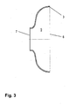
- Fig. 3 a first possibility for the following step of forming the disc 4 to a half-cell 5 is shown.
- the forming of the disc 4 is preferably carried out by pressing, deep drawing and optionally rolling, wherein the in Fig. 3 Half-cell 5 shown in cross section and one in Fig. 5 half-cell 5 'shown in cross-section are formed accordingly.
- a forming intermediate step in which the surface of the disc is first increased and / or the creation of a hollow truncated cone with two parallel open end faces, is possible.
- the half-cell 5 also has a joining surface 6 and a closing surface 7. In this case, the joining surface 6 and the end surface 7 preferably run parallel to one another.
- the marker 3 is mounted on the disc 4 so that it is still visible after forming a disc 4 to a half-cell 5.
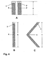
- a second possibility for the forming of the discs 4, 4 ' is shown.
- the forming includes the creation of a hollow cone by deep drawing or pressing, wherein the pressing takes place against a negative mold.
- the discs 4, 4 ' which initially have a diameter a, before forming, for example, a cone or a truncated cone are first converted by means of rolling or pressing to discs 4, which have a diameter b which is greater than a.
- the largest diameter c of the hollow cone after forming is greater than or equal to the outer diameter of the half-cell 5. This makes it possible to bring the hollow cone with the smallest possible number of processing steps to the desired shape and size of the later half-cell 5, without the monocrystalline properties the material is lost.
- Fig. 5 a cross-sectional view of a hollow body 8 is shown, which has been assembled from two half-cells 5 and 5 'with markings 3 and 3' along the two joining surfaces 6 and 6 ', which is preferably by electron beam welding in a high vacuum ( ⁇ 10 -4 mbar) and further preferred happens at a defined residual gas composition.
- the half cells 5 and 5 ' can be welded with a smooth seam that is 5 to 7 mm wide, resulting in only a localized energy input.
- this technique ensures that the weld is absolutely tight.
- the joining surfaces 6 and 6 'of two half-cells 5 and 5' have been joined together so that the half-cells 5 and 5 'are arranged adjacent to each other from originally in the substrate 1 adjacent discs 4 and 4', with the joining surfaces 6 and 6 'adjacent Markers 3 and 3 'are arranged to each other, as was the case on both sides of the cut surface 2 between the discs 4 and 4'.
- the consisting of the composite half-cells 5 and 5 'hollow body 8 has two mutually substantially parallel end surfaces 7 and 7'.
- the hollow body 8 produced from the half-cells 5, 5 ' exists over the entire volume, also in the region of the earlier joining surfaces 6, 6', of monocrystalline material Material so that it has good electrical properties and flow in the surface layer of the superconductor (niobium) circulating currents, which prevent an external magnetic field from penetrating into the interior, whereby the superconductivity is disturbed.
- the superconductor niobium
- the joining surfaces 6 and 6 'and / or end surfaces 7 and 7' are cleaned prior to joining. These surfaces are first rinsed and treated in an ultrasonic bath, then preferably by a chemical process with BCP (1: 1: 2) pickled to remove contaminants in this area, rinsed again with ultrapure water and finally dried in a clean room.
- a special heat treatment of the hollow body 8 can take place, which can be heated at 400 ° C. to 500 ° C. for a period of two to six hours and then heated up to 750 ° over a period of one to three hours C to 850 ° C, preferably 750 ° to 800 ° C comprises.
- the aim of the first heating step is to reduce the stresses created by the transformations and to eliminate newly formed nuclei.
- the second heating step serves to remove existing hydrogen from the material and to relax the entire hollow body.
- the monocrystalline hollow bodies 8 thus produced have excellent electrical properties, in which circulating currents are present in the monocrystalline surface layer of the superconductor (niobium), which prevent an external magnetic field from penetrating into the interior, whereby a superconductivity is not disturbed.
- the monocrystalline material significantly lower roughness in particular the inner Surface at 25 nm in the case of a final BCP treatment.
- Fig. 6 shows a plurality of hollow bodies 8, 8 ', 8'', which have been prepared according to the method described above and analogous to the joining of two half-cells 5 and 5' to a hollow body 8 at their end faces 7 ', 7'',7'' , 7 '''' have been joined together, preferably also by electron beam welding.
- the resonator 9 produced by assembling a plurality of hollow bodies 8, 8 ', 8 can be polished, preferably by a chemical process with BCP (1: 1: 2).
- dumbbell-shaped hollow bodies are first formed, which are then joined together to form the resonator 9.
- a single-crystal resonator 9 having improved electrical properties can be produced. These have the effect of significantly improving the quality of superconductivity under suitable environmental conditions, such as a suitable temperature. Furthermore, the advantage lies in the use of a monocrystalline resonator 9 The fact that a much better surface quality (smoothness) can be achieved even by the simple chemical pickling process, even compared to electropolishing.
Claims (22)
- Procédé de fabrication de corps creux pour résonateurs, comprenant les étapes suivantes :- préparer un substrat (1) avec une zone monocristalline,- définir une surface de coupe (2) à travers le substrat (1),- placer des repères (3, 3') des deux côtés de la surface de coupe (2),- réaliser deux disques (4, 4') par découpe le long de la surface de coupe (2), les disques (4, 4') étant prélevés entièrement de la zone monocristalline,- déformer les disques (4, 4') en demi-cellules (5, 5'), les demi-cellules (5, 5') présentant une surface d'assemblage (6, 6'),- assembler les demi-cellules (5, 5') en un corps creux (8), les surfaces d'assemblage (6, 6') s'appliquant l'une contre l'autre et les repères (3, 3') sur les demi-cellules (5, 5'), des deux côtés de la surface d'assemblage (6, 6'), étant orientés l'un vers l'autre de la même manière que sur les deux côtés des surfaces de coupe (2, 2').
- Procédé selon la revendication 1, dans lequel les demi-cellules (5, 5') présentent une surface de terminaison qui s'étend parallèlement aux surfaces d'assemblage (6, 6').
- Procédé selon l'une quelconque des revendications 1 ou 2, dans lequel le substrat (1) comporte un matériau supraconducteur.
- Procédé selon l'une quelconque des revendications 1 3, dans lequel le substrat (1) comporte du Niobium.
- Procédé selon l'une quelconque des revendications 1 à 4, dans lequel la zone monocristalline est cylindrique.
- Procédé selon l'une quelconque des revendications 1 à 5, dans lequel les repères (3, 3') sont estampés ou gaufrés.
- Procédé selon l'une quelconque des revendications 1 à 6, dans lequel les disques (4, 4') présentent une épaisseur d'environ 5 mm et s'étendent sur 200 mm dans le plan de la surface de coupe (2, 2').
- Procédé selon l'une quelconque des revendications 1 à 7, dans lequel la surface des disques (4, 4') est agrandie après la coupe.
- Procédé selon l'une quelconque des revendications 1 à 8, dans lequel la déformation s'effectue par repoussage, emboutissage profond et le cas échéant par laminage.
- Procédé selon la revendication 9, dans lequel la déformation comprend la réalisation d'un tronc de cône creux avec deux surfaces de terminaison ouvertes parallèles.
- Procédé selon l'une quelconque des revendications 1 à 9, dans lequel la déformation comprend la réalisation d'un cône creux.
- Procédé selon la revendication 11, dans lequel le plus grand diamètre du cône creux est supérieur ou égal au diamètre extérieur des demi-cellules (5, 5').
- Procédé selon l'une quelconque des revendications 1 à 12, dans lequel les demi-cellules (5, 5') présentent une symétrie de révolution.
- Procédé selon l'une quelconque des revendications 1 à 13, dans lequel l'assemblage s'effectue par soudage à faisceau d'électrons.
- Procédé selon l'une quelconque des revendications 1 à 14, dans lequel les surfaces d'assemblage (6, 6') et/ou les surfaces de terminaison (7, 7') sont nettoyées avant l'assemblage.
- Procédé selon la revendication 15, dans lequel les surfaces d'assemblage (6, 6') et/ou les surfaces de terminaison (7, 7') sont décapées chimiquement.
- Procédé selon l'une quelconque des revendications 1 à 16, dans lequel il est procédé à un traitement thermique du corps creux (8).
- Procédé selon la revendication 17, dans lequel le traitement thermique consiste à chauffer pendant un intervalle de temps de deux à six heures à une température comprise entre 400°C et 500°C, puis à chauffer pendant un intervalle de temps de une à trois heures à une température comprise entre 750°C et 850°C.
- Procédé selon la revendication 17, dans lequel le traitement thermique consiste à chauffer pendant un intervalle de temps de deux à six heures à une température comprise entre 400°C et 500°C, puis à chauffer pendant un intervalle de temps de une à trois heures à une température comprise entre 700°C et 800°C.
- Procédé de fabrication d'un résonateur (9), comprenant les étapes suivantes:- fabriquer un grand nombre de corps creux (8, 8', 8"...) selon l'une quelconque des revendications 2 à 19,- assembler les corps creux (8, 8', 8") le long des surfaces de terminaison (7, 7', 7", 7"', 7""), des demi-cellules (5', 5", 5"', 5"") de disques initialement voisins dans le substrat (1) sont reliées, et les repères, voisins aux surfaces de terminaison (7, 7', 7", 7"', 7"", 7""') sont associés les uns aux autres comme sur les deux côtés de la surface de coupe (2, 2') entre les disques (4, 4').
- Procédé selon la revendication 20, dans lequel le résonateur (9) est nettoyé.
- Procédé selon la revendication 21, dans lequel le résonateur (9) est décapé chimiquement.
Applications Claiming Priority (3)
| Application Number | Priority Date | Filing Date | Title |
|---|---|---|---|
| DE102005058398 | 2005-12-02 | ||
| DE102006021111A DE102006021111B3 (de) | 2005-12-02 | 2006-05-05 | Verfahren zur Herstellung von Hohlkörpern von Resonatoren |
| PCT/EP2006/011464 WO2007062829A1 (fr) | 2005-12-02 | 2006-11-29 | Procédé de fabrication de corps creux pour des résonateurs |
Publications (2)
| Publication Number | Publication Date |
|---|---|
| EP1955404A1 EP1955404A1 (fr) | 2008-08-13 |
| EP1955404B1 true EP1955404B1 (fr) | 2009-03-18 |
Family
ID=37671243
Family Applications (1)
| Application Number | Title | Priority Date | Filing Date |
|---|---|---|---|
| EP06818910A Active EP1955404B1 (fr) | 2005-12-02 | 2006-11-29 | Procédé de fabrication de corps creux pour des résonateurs |
Country Status (6)
| Country | Link |
|---|---|
| US (1) | US8088714B2 (fr) |
| EP (1) | EP1955404B1 (fr) |
| JP (1) | JP5320068B2 (fr) |
| AT (1) | ATE426255T1 (fr) |
| DE (2) | DE102006021111B3 (fr) |
| WO (1) | WO2007062829A1 (fr) |
Families Citing this family (9)
| Publication number | Priority date | Publication date | Assignee | Title |
|---|---|---|---|---|
| US9352416B2 (en) * | 2009-11-03 | 2016-05-31 | The Secretary, Department Of Atomic Energy, Govt. Of India | Niobium based superconducting radio frequency(SCRF) cavities comprising niobium components joined by laser welding, method and apparatus for manufacturing such cavities |
| JP5804840B2 (ja) * | 2011-08-11 | 2015-11-04 | 三菱重工業株式会社 | 加工装置及び加工方法 |
| US11071194B2 (en) | 2016-07-21 | 2021-07-20 | Fermi Research Alliance, Llc | Longitudinally joined superconducting resonating cavities |
| EP3346017B1 (fr) * | 2017-01-10 | 2021-09-15 | Heraeus Deutschland GmbH & Co. KG | Procédé de coupe de métaux réfractaires |
| US10847860B2 (en) | 2018-05-18 | 2020-11-24 | Ii-Vi Delaware, Inc. | Superconducting resonating cavity and method of production thereof |
| US10856402B2 (en) | 2018-05-18 | 2020-12-01 | Ii-Vi Delaware, Inc. | Superconducting resonating cavity with laser welded seam and method of formation thereof |
| US11464102B2 (en) * | 2018-10-06 | 2022-10-04 | Fermi Research Alliance, Llc | Methods and systems for treatment of superconducting materials to improve low field performance |
| CN109462932B (zh) * | 2018-12-28 | 2021-04-06 | 上海联影医疗科技股份有限公司 | 一种驻波加速管 |
| CN113355671B (zh) * | 2021-06-10 | 2022-12-13 | 兰州荣翔轨道交通科技有限公司 | 基于数控车床的纯铌超导腔表面铜铌改性层制备方法 |
Family Cites Families (9)
| Publication number | Priority date | Publication date | Assignee | Title |
|---|---|---|---|---|
| DE3608160A1 (de) * | 1986-03-12 | 1987-09-24 | Kernforschungsz Karlsruhe | Verfahren zur herstellung supraleitender hohlraumresonatoren |
| DE3722745A1 (de) * | 1987-07-09 | 1989-01-19 | Interatom | Herstellungsverfahren fuer hohlkoerper aus beschichteten blechen und apparat, insbesondere supraleitender hochfrequenz-resonator |
| JPH03135000A (ja) | 1989-10-20 | 1991-06-07 | Furukawa Electric Co Ltd:The | 超伝導加速管 |
| JPH03147299A (ja) | 1989-11-01 | 1991-06-24 | Furukawa Electric Co Ltd:The | 超伝導加速空洞の製造方法 |
| US5239157A (en) | 1990-10-31 | 1993-08-24 | The Furukawa Electric Co., Ltd. | Superconducting accelerating tube and a method for manufacturing the same |
| WO1992013434A1 (fr) * | 1991-01-24 | 1992-08-06 | The Furukawa Electric Co., Ltd. | Conduit d'acceleration supraconducteur |
| JP3089085B2 (ja) | 1992-03-23 | 2000-09-18 | 三菱重工業株式会社 | 電子ビーム用超伝導加速空洞の製造方法 |
| DE69310722T2 (de) * | 1993-06-14 | 1997-09-11 | Ist Nazionale Fisica Nucleare | Herstellungsverfahren von nahtloser Radiofrequenz-Resonanzholräumen und dadurch erhaltenes Produkt |
| US7746192B2 (en) * | 2005-06-20 | 2010-06-29 | The Texas A&M University System | Polyhedral contoured microwave cavities |
-
2006
- 2006-05-05 DE DE102006021111A patent/DE102006021111B3/de not_active Expired - Fee Related
- 2006-11-29 US US12/095,901 patent/US8088714B2/en active Active
- 2006-11-29 EP EP06818910A patent/EP1955404B1/fr active Active
- 2006-11-29 JP JP2008542660A patent/JP5320068B2/ja active Active
- 2006-11-29 DE DE502006003219T patent/DE502006003219D1/de active Active
- 2006-11-29 WO PCT/EP2006/011464 patent/WO2007062829A1/fr active Application Filing
- 2006-11-29 AT AT06818910T patent/ATE426255T1/de not_active IP Right Cessation
Also Published As
| Publication number | Publication date |
|---|---|
| DE102006021111B3 (de) | 2007-08-02 |
| ATE426255T1 (de) | 2009-04-15 |
| WO2007062829A1 (fr) | 2007-06-07 |
| EP1955404A1 (fr) | 2008-08-13 |
| JP2009517817A (ja) | 2009-04-30 |
| US20090215631A1 (en) | 2009-08-27 |
| US8088714B2 (en) | 2012-01-03 |
| JP5320068B2 (ja) | 2013-10-23 |
| DE502006003219D1 (de) | 2009-04-30 |
Similar Documents
| Publication | Publication Date | Title |
|---|---|---|
| EP1955404B1 (fr) | Procédé de fabrication de corps creux pour des résonateurs | |
| DE60214683T2 (de) | Platten aus refraktärem metall mit einheitlicher textur und verfahren zu ihrer herstellung | |
| DE60124385T2 (de) | Verfahren zum verbinden eines targets auf einer trägerplatte | |
| DE3318766C2 (fr) | ||
| CH655951A5 (de) | Superlegierungsblech auf nickelbasis und verfahren zu dessen herstellung. | |
| WO2010012255A2 (fr) | Procédé pour produire un joint d'assemblage avec une matière monocristalline ou à solidification directionnelle | |
| DE3933713A1 (de) | Verfahren zur bildung einer leitenden metallschicht auf einem anorganischen substrat | |
| EP3570973B1 (fr) | Procédé de fabrication additive | |
| DE112010002097T5 (de) | Sputtertarget und Verfahren zur Verarbeitung elnes Sputtertarget | |
| DE1927825A1 (de) | Verfahren zur Herstellung von supraleitenden Hohlraumresonatoren,insbesondere fuer Teilchenbeschleuniger | |
| DE1963644A1 (de) | Verfahren zum Herstellen von Teilen mit Loechern oder Vertiefungen | |
| DE102015111897A1 (de) | Verfahren zum Herstellen eines Seltenerdmagnets | |
| DE69829396T2 (de) | Teilchenbeschleuniger-hohlraum mit verstärktem supraleitendem material, und herstellungsverfahren | |
| WO2018058158A1 (fr) | Cible de pulvérisation cathodique | |
| EP3352236B1 (fr) | Procédé de fabrication d'une structure réalisée en au moins deux parties, en particulier d'un demi-produit pour un fil supraconducteur | |
| EP2566572B1 (fr) | Electrode et procede de fabrication d'une telle electrode | |
| EP3346017B1 (fr) | Procédé de coupe de métaux réfractaires | |
| EP1641591A1 (fr) | Procede pour separer des pieces planes en ceramique avec une longueur de tache d'irradiation calculee | |
| DE10018244A1 (de) | Verfahren zum Polieren einer Oberfläche eines superleitenden Hohlraums | |
| DE1916293A1 (de) | Verfahren zum Herstellen einer Niobschicht durch schmelzflusselektrolytische Abscheidung auf einem Kupfertraeger | |
| DE102019112579A1 (de) | Supraleitender Resonanzhohlraum mit lasergeschweißter Naht und Verfahren zur Bildung davon | |
| CH525044A (de) | Verfahren zur Herstellung von Folien, Bändern und Profilteilen aus Metall oder Metall-Glas-Schichtwerkstoffen | |
| WO2022058461A2 (fr) | Procédé de fabrication et de conception d'éléments de blindage magnétiques tridimensionnels complexes, éléments de blindage et leur utilisation | |
| EP2526563B1 (fr) | Procédé de fabrication d'une électrode pour une lampe à décharge à haute pression et lampe à décharge à haute pression comprenant au moins une électrode ainsi fabriquée | |
| WO2022018227A1 (fr) | Procédé de fabrication d'un élément de contact formé au moins par endroits à partir d'un alliage de laiton, et élément de contact |
Legal Events
| Date | Code | Title | Description |
|---|---|---|---|
| PUAI | Public reference made under article 153(3) epc to a published international application that has entered the european phase |
Free format text: ORIGINAL CODE: 0009012 |
|
| 17P | Request for examination filed |
Effective date: 20080613 |
|
| AK | Designated contracting states |
Kind code of ref document: A1 Designated state(s): AT BE BG CH CY CZ DE DK EE ES FI FR GB GR HU IE IS IT LI LT LU LV MC NL PL PT RO SE SI SK TR |
|
| GRAP | Despatch of communication of intention to grant a patent |
Free format text: ORIGINAL CODE: EPIDOSNIGR1 |
|
| DAX | Request for extension of the european patent (deleted) | ||
| GRAS | Grant fee paid |
Free format text: ORIGINAL CODE: EPIDOSNIGR3 |
|
| GRAA | (expected) grant |
Free format text: ORIGINAL CODE: 0009210 |
|
| AK | Designated contracting states |
Kind code of ref document: B1 Designated state(s): AT BE BG CH CY CZ DE DK EE ES FI FR GB GR HU IE IS IT LI LT LU LV MC NL PL PT RO SE SI SK TR |
|
| REG | Reference to a national code |
Ref country code: GB Ref legal event code: FG4D Free format text: NOT ENGLISH |
|
| REG | Reference to a national code |
Ref country code: CH Ref legal event code: EP Ref country code: CH Ref legal event code: NV Representative=s name: E. BLUM & CO. AG PATENT- UND MARKENANWAELTE VSP |
|
| REG | Reference to a national code |
Ref country code: IE Ref legal event code: FG4D Free format text: LANGUAGE OF EP DOCUMENT: GERMAN |
|
| REF | Corresponds to: |
Ref document number: 502006003219 Country of ref document: DE Date of ref document: 20090430 Kind code of ref document: P |
|
| PG25 | Lapsed in a contracting state [announced via postgrant information from national office to epo] |
Ref country code: LT Free format text: LAPSE BECAUSE OF FAILURE TO SUBMIT A TRANSLATION OF THE DESCRIPTION OR TO PAY THE FEE WITHIN THE PRESCRIBED TIME-LIMIT Effective date: 20090318 Ref country code: SI Free format text: LAPSE BECAUSE OF FAILURE TO SUBMIT A TRANSLATION OF THE DESCRIPTION OR TO PAY THE FEE WITHIN THE PRESCRIBED TIME-LIMIT Effective date: 20090318 Ref country code: FI Free format text: LAPSE BECAUSE OF FAILURE TO SUBMIT A TRANSLATION OF THE DESCRIPTION OR TO PAY THE FEE WITHIN THE PRESCRIBED TIME-LIMIT Effective date: 20090318 Ref country code: NL Free format text: LAPSE BECAUSE OF FAILURE TO SUBMIT A TRANSLATION OF THE DESCRIPTION OR TO PAY THE FEE WITHIN THE PRESCRIBED TIME-LIMIT Effective date: 20090318 |
|
| PG25 | Lapsed in a contracting state [announced via postgrant information from national office to epo] |
Ref country code: SE Free format text: LAPSE BECAUSE OF FAILURE TO SUBMIT A TRANSLATION OF THE DESCRIPTION OR TO PAY THE FEE WITHIN THE PRESCRIBED TIME-LIMIT Effective date: 20090618 Ref country code: PL Free format text: LAPSE BECAUSE OF FAILURE TO SUBMIT A TRANSLATION OF THE DESCRIPTION OR TO PAY THE FEE WITHIN THE PRESCRIBED TIME-LIMIT Effective date: 20090318 Ref country code: LV Free format text: LAPSE BECAUSE OF FAILURE TO SUBMIT A TRANSLATION OF THE DESCRIPTION OR TO PAY THE FEE WITHIN THE PRESCRIBED TIME-LIMIT Effective date: 20090318 |
|
| NLV1 | Nl: lapsed or annulled due to failure to fulfill the requirements of art. 29p and 29m of the patents act | ||
| REG | Reference to a national code |
Ref country code: IE Ref legal event code: FD4D |
|
| PG25 | Lapsed in a contracting state [announced via postgrant information from national office to epo] |
Ref country code: EE Free format text: LAPSE BECAUSE OF FAILURE TO SUBMIT A TRANSLATION OF THE DESCRIPTION OR TO PAY THE FEE WITHIN THE PRESCRIBED TIME-LIMIT Effective date: 20090318 Ref country code: IE Free format text: LAPSE BECAUSE OF FAILURE TO SUBMIT A TRANSLATION OF THE DESCRIPTION OR TO PAY THE FEE WITHIN THE PRESCRIBED TIME-LIMIT Effective date: 20090318 Ref country code: ES Free format text: LAPSE BECAUSE OF FAILURE TO SUBMIT A TRANSLATION OF THE DESCRIPTION OR TO PAY THE FEE WITHIN THE PRESCRIBED TIME-LIMIT Effective date: 20090629 Ref country code: CZ Free format text: LAPSE BECAUSE OF FAILURE TO SUBMIT A TRANSLATION OF THE DESCRIPTION OR TO PAY THE FEE WITHIN THE PRESCRIBED TIME-LIMIT Effective date: 20090318 Ref country code: PT Free format text: LAPSE BECAUSE OF FAILURE TO SUBMIT A TRANSLATION OF THE DESCRIPTION OR TO PAY THE FEE WITHIN THE PRESCRIBED TIME-LIMIT Effective date: 20090827 |
|
| PG25 | Lapsed in a contracting state [announced via postgrant information from national office to epo] |
Ref country code: IS Free format text: LAPSE BECAUSE OF FAILURE TO SUBMIT A TRANSLATION OF THE DESCRIPTION OR TO PAY THE FEE WITHIN THE PRESCRIBED TIME-LIMIT Effective date: 20090718 Ref country code: RO Free format text: LAPSE BECAUSE OF FAILURE TO SUBMIT A TRANSLATION OF THE DESCRIPTION OR TO PAY THE FEE WITHIN THE PRESCRIBED TIME-LIMIT Effective date: 20090318 Ref country code: SK Free format text: LAPSE BECAUSE OF FAILURE TO SUBMIT A TRANSLATION OF THE DESCRIPTION OR TO PAY THE FEE WITHIN THE PRESCRIBED TIME-LIMIT Effective date: 20090318 |
|
| PLBE | No opposition filed within time limit |
Free format text: ORIGINAL CODE: 0009261 |
|
| STAA | Information on the status of an ep patent application or granted ep patent |
Free format text: STATUS: NO OPPOSITION FILED WITHIN TIME LIMIT |
|
| PG25 | Lapsed in a contracting state [announced via postgrant information from national office to epo] |
Ref country code: DK Free format text: LAPSE BECAUSE OF FAILURE TO SUBMIT A TRANSLATION OF THE DESCRIPTION OR TO PAY THE FEE WITHIN THE PRESCRIBED TIME-LIMIT Effective date: 20090318 Ref country code: BG Free format text: LAPSE BECAUSE OF FAILURE TO SUBMIT A TRANSLATION OF THE DESCRIPTION OR TO PAY THE FEE WITHIN THE PRESCRIBED TIME-LIMIT Effective date: 20090618 |
|
| 26N | No opposition filed |
Effective date: 20091221 |
|
| BERE | Be: lapsed |
Owner name: DEUTSCHES ELEKTRONEN-SYNCHROTRON DESY Effective date: 20091130 |
|
| PG25 | Lapsed in a contracting state [announced via postgrant information from national office to epo] |
Ref country code: MC Free format text: LAPSE BECAUSE OF NON-PAYMENT OF DUE FEES Effective date: 20091130 |
|
| PG25 | Lapsed in a contracting state [announced via postgrant information from national office to epo] |
Ref country code: GR Free format text: LAPSE BECAUSE OF FAILURE TO SUBMIT A TRANSLATION OF THE DESCRIPTION OR TO PAY THE FEE WITHIN THE PRESCRIBED TIME-LIMIT Effective date: 20090619 Ref country code: BE Free format text: LAPSE BECAUSE OF NON-PAYMENT OF DUE FEES Effective date: 20091130 |
|
| PG25 | Lapsed in a contracting state [announced via postgrant information from national office to epo] |
Ref country code: AT Free format text: LAPSE BECAUSE OF NON-PAYMENT OF DUE FEES Effective date: 20091129 |
|
| PG25 | Lapsed in a contracting state [announced via postgrant information from national office to epo] |
Ref country code: LU Free format text: LAPSE BECAUSE OF NON-PAYMENT OF DUE FEES Effective date: 20091129 |
|
| PG25 | Lapsed in a contracting state [announced via postgrant information from national office to epo] |
Ref country code: HU Free format text: LAPSE BECAUSE OF FAILURE TO SUBMIT A TRANSLATION OF THE DESCRIPTION OR TO PAY THE FEE WITHIN THE PRESCRIBED TIME-LIMIT Effective date: 20090919 |
|
| PG25 | Lapsed in a contracting state [announced via postgrant information from national office to epo] |
Ref country code: TR Free format text: LAPSE BECAUSE OF FAILURE TO SUBMIT A TRANSLATION OF THE DESCRIPTION OR TO PAY THE FEE WITHIN THE PRESCRIBED TIME-LIMIT Effective date: 20090318 |
|
| PG25 | Lapsed in a contracting state [announced via postgrant information from national office to epo] |
Ref country code: CY Free format text: LAPSE BECAUSE OF FAILURE TO SUBMIT A TRANSLATION OF THE DESCRIPTION OR TO PAY THE FEE WITHIN THE PRESCRIBED TIME-LIMIT Effective date: 20090318 |
|
| REG | Reference to a national code |
Ref country code: FR Ref legal event code: PLFP Year of fee payment: 10 |
|
| REG | Reference to a national code |
Ref country code: FR Ref legal event code: PLFP Year of fee payment: 11 |
|
| REG | Reference to a national code |
Ref country code: FR Ref legal event code: PLFP Year of fee payment: 12 |
|
| REG | Reference to a national code |
Ref country code: FR Ref legal event code: PLFP Year of fee payment: 13 |
|
| PGFP | Annual fee paid to national office [announced via postgrant information from national office to epo] |
Ref country code: GB Payment date: 20231123 Year of fee payment: 18 |
|
| PGFP | Annual fee paid to national office [announced via postgrant information from national office to epo] |
Ref country code: IT Payment date: 20231130 Year of fee payment: 18 Ref country code: FR Payment date: 20231122 Year of fee payment: 18 Ref country code: DE Payment date: 20231120 Year of fee payment: 18 Ref country code: CH Payment date: 20231201 Year of fee payment: 18 |