EP1939673B1 - Flüssigkristallanzeigevorrichtung und Herstellungsverfahren dafür - Google Patents
Flüssigkristallanzeigevorrichtung und Herstellungsverfahren dafür Download PDFInfo
- Publication number
- EP1939673B1 EP1939673B1 EP07122936A EP07122936A EP1939673B1 EP 1939673 B1 EP1939673 B1 EP 1939673B1 EP 07122936 A EP07122936 A EP 07122936A EP 07122936 A EP07122936 A EP 07122936A EP 1939673 B1 EP1939673 B1 EP 1939673B1
- Authority
- EP
- European Patent Office
- Prior art keywords
- electrode
- gate
- forming
- data line
- disposed
- Prior art date
- Legal status (The legal status is an assumption and is not a legal conclusion. Google has not performed a legal analysis and makes no representation as to the accuracy of the status listed.)
- Active
Links
Images





Classifications
-
- G—PHYSICS
- G02—OPTICS
- G02F—OPTICAL DEVICES OR ARRANGEMENTS FOR THE CONTROL OF LIGHT BY MODIFICATION OF THE OPTICAL PROPERTIES OF THE MEDIA OF THE ELEMENTS INVOLVED THEREIN; NON-LINEAR OPTICS; FREQUENCY-CHANGING OF LIGHT; OPTICAL LOGIC ELEMENTS; OPTICAL ANALOGUE/DIGITAL CONVERTERS
- G02F1/00—Devices or arrangements for the control of the intensity, colour, phase, polarisation or direction of light arriving from an independent light source, e.g. switching, gating or modulating; Non-linear optics
- G02F1/01—Devices or arrangements for the control of the intensity, colour, phase, polarisation or direction of light arriving from an independent light source, e.g. switching, gating or modulating; Non-linear optics for the control of the intensity, phase, polarisation or colour
- G02F1/13—Devices or arrangements for the control of the intensity, colour, phase, polarisation or direction of light arriving from an independent light source, e.g. switching, gating or modulating; Non-linear optics for the control of the intensity, phase, polarisation or colour based on liquid crystals, e.g. single liquid crystal display cells
- G02F1/133—Constructional arrangements; Operation of liquid crystal cells; Circuit arrangements
- G02F1/1333—Constructional arrangements; Manufacturing methods
- G02F1/1343—Electrodes
- G02F1/134309—Electrodes characterised by their geometrical arrangement
- G02F1/134363—Electrodes characterised by their geometrical arrangement for applying an electric field parallel to the substrate, i.e. in-plane switching [IPS]
-
- G—PHYSICS
- G02—OPTICS
- G02F—OPTICAL DEVICES OR ARRANGEMENTS FOR THE CONTROL OF LIGHT BY MODIFICATION OF THE OPTICAL PROPERTIES OF THE MEDIA OF THE ELEMENTS INVOLVED THEREIN; NON-LINEAR OPTICS; FREQUENCY-CHANGING OF LIGHT; OPTICAL LOGIC ELEMENTS; OPTICAL ANALOGUE/DIGITAL CONVERTERS
- G02F1/00—Devices or arrangements for the control of the intensity, colour, phase, polarisation or direction of light arriving from an independent light source, e.g. switching, gating or modulating; Non-linear optics
- G02F1/01—Devices or arrangements for the control of the intensity, colour, phase, polarisation or direction of light arriving from an independent light source, e.g. switching, gating or modulating; Non-linear optics for the control of the intensity, phase, polarisation or colour
- G02F1/13—Devices or arrangements for the control of the intensity, colour, phase, polarisation or direction of light arriving from an independent light source, e.g. switching, gating or modulating; Non-linear optics for the control of the intensity, phase, polarisation or colour based on liquid crystals, e.g. single liquid crystal display cells
- G02F1/133—Constructional arrangements; Operation of liquid crystal cells; Circuit arrangements
- G02F1/1333—Constructional arrangements; Manufacturing methods
- G02F1/1343—Electrodes
-
- G—PHYSICS
- G02—OPTICS
- G02F—OPTICAL DEVICES OR ARRANGEMENTS FOR THE CONTROL OF LIGHT BY MODIFICATION OF THE OPTICAL PROPERTIES OF THE MEDIA OF THE ELEMENTS INVOLVED THEREIN; NON-LINEAR OPTICS; FREQUENCY-CHANGING OF LIGHT; OPTICAL LOGIC ELEMENTS; OPTICAL ANALOGUE/DIGITAL CONVERTERS
- G02F1/00—Devices or arrangements for the control of the intensity, colour, phase, polarisation or direction of light arriving from an independent light source, e.g. switching, gating or modulating; Non-linear optics
- G02F1/01—Devices or arrangements for the control of the intensity, colour, phase, polarisation or direction of light arriving from an independent light source, e.g. switching, gating or modulating; Non-linear optics for the control of the intensity, phase, polarisation or colour
- G02F1/13—Devices or arrangements for the control of the intensity, colour, phase, polarisation or direction of light arriving from an independent light source, e.g. switching, gating or modulating; Non-linear optics for the control of the intensity, phase, polarisation or colour based on liquid crystals, e.g. single liquid crystal display cells
- G02F1/133—Constructional arrangements; Operation of liquid crystal cells; Circuit arrangements
- G02F1/1333—Constructional arrangements; Manufacturing methods
- G02F1/1343—Electrodes
- G02F1/134309—Electrodes characterised by their geometrical arrangement
- G02F1/134372—Electrodes characterised by their geometrical arrangement for fringe field switching [FFS] where the common electrode is not patterned
-
- G—PHYSICS
- G02—OPTICS
- G02F—OPTICAL DEVICES OR ARRANGEMENTS FOR THE CONTROL OF LIGHT BY MODIFICATION OF THE OPTICAL PROPERTIES OF THE MEDIA OF THE ELEMENTS INVOLVED THEREIN; NON-LINEAR OPTICS; FREQUENCY-CHANGING OF LIGHT; OPTICAL LOGIC ELEMENTS; OPTICAL ANALOGUE/DIGITAL CONVERTERS
- G02F1/00—Devices or arrangements for the control of the intensity, colour, phase, polarisation or direction of light arriving from an independent light source, e.g. switching, gating or modulating; Non-linear optics
- G02F1/01—Devices or arrangements for the control of the intensity, colour, phase, polarisation or direction of light arriving from an independent light source, e.g. switching, gating or modulating; Non-linear optics for the control of the intensity, phase, polarisation or colour
- G02F1/13—Devices or arrangements for the control of the intensity, colour, phase, polarisation or direction of light arriving from an independent light source, e.g. switching, gating or modulating; Non-linear optics for the control of the intensity, phase, polarisation or colour based on liquid crystals, e.g. single liquid crystal display cells
- G02F1/133—Constructional arrangements; Operation of liquid crystal cells; Circuit arrangements
- G02F1/136—Liquid crystal cells structurally associated with a semi-conducting layer or substrate, e.g. cells forming part of an integrated circuit
- G02F1/1362—Active matrix addressed cells
- G02F1/136213—Storage capacitors associated with the pixel electrode
Definitions
- the present invention relates to a fringe field type flat panel display panel and a fabricating method thereof, and more particularly to a fringe field type liquid crystal display panel and a fabricating method thereof that is adaptive for increasing an aperture ratio of a pixel area by forming a common electrode to be overlapped with a data line.
- a liquid crystal display panel controls the light transmittance of liquid crystal by use of electric field, thereby displaying a picture.
- the liquid crystal display panel is broadly classified into a vertical electric field applying type and a horizontal electric field applying type in accordance with the direction of the electric field which drives the liquid crystal.
- the vertical electric field applying type liquid crystal display panel drives a liquid crystal of a twisted nematic (hereinafter, referred to as "TN") mode by a vertical electric field formed between a common electrode and a pixel electrode which are arranged to face each other in upper and lower substrates.
- the vertical electric field applying type liquid crystal display panel has an advantage in that its aperture ratio is high, but has a disadvantage in that its viewing angle is narrow to be about 90°.
- the horizontal electric field applying type liquid crystal display panel drives a liquid crystal of an in-plain switching (hereinafter, referred to as "IPS") mode by a horizontal electric field formed between a common electrode and a pixel electrode which are arranged in parallel in a lower substrate.
- IPS in-plain switching
- the horizontal electric field applying type liquid crystal display panel has an advantage in that its viewing angle is broad to be about 160°, but has a disadvantage in that its aperture ratio and transmittance are low.
- the FFS type liquid crystal display panel includes a common electrode plate and a pixel electrode with an insulating film therebetween in each pixel area, and forms a gap between the common electrode plate and the pixel electrode to be narrower than the gap between the upper and lower substrates, thereby forming a fringe field for driving liquid crystal molecules filled between the upper and lower substrates.
- the fringe field is formed even in a pixel area adjacent to a data line to drive a liquid crystal, thus light leaks out between the data line and the pixel electrode adjacent thereto, i.e., vertical cross talk.
- US 6,449,026 B1 discloses a fringe field type liquid crystal display panel, wherein a drain electrode of a thin film transistor directly covers one end of the pixel electrode.
- the invention provides a fringe field type liquid crystal display panel according to claim 1.
- the invention provides a fabricating method of a fringe field type liquid crystal display panel according to claim 16.
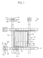
- FIG. 1 is a plan view of a fringe field type flat panel display panel according to the present invention.
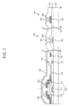
- FIG. 2 is a configurational sectional view of a fringe field type flat panel display panel according to the present invention.
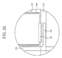
- FIGs. 3A and 3B are configurational plan views of a thin film transistor formed in a fringe field type liquid crystal display panel according to the present invention.
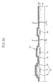
- FIGs. 4A and 4B are a plan view and a cross sectional view of a flat panel display panel where a first conductive pattern is formed according to the present invention.
- FIGs. 5A and 5B are a plan view and a cross sectional view of a flat panel display panel where a pixel electrode is formed according to the present invention.
- FIGs. 6A and 6B are a plan view and a cross sectional view of a flat panel display panel where a semiconductor layer is formed according to the present invention.
- FIGs. 7A and 7B are a plan view and a cross sectional view of a flat panel display panel where a second conductive pattern is formed according to the present invention.
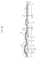
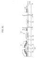
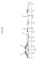
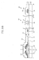
- FIGs. 8A and 8G are process diagrams illustrating a process of forming a second conductive pattern according to the present invention.
- FIGs. 9A and 9B are a plan view and a cross sectional view of a flat panel display panel where a passivation film having a contact hole is formed according to the present invention.
- FIGs. 10A and 10B are a plan view and a cross sectional view of a flat panel display panel where a third conductive pattern is formed according to the present invention.
- FIGS. 1 and 2 depict a fringe field type liquid crystal display panel 100 according to the present invention that includes a gate line 110 formed on a substrate 102; a data line 120 formed to cross a gate line 110 with a gate insulating film 115 therebetween to define a pixel area 142; a thin film transistor T formed at a crossing area of the gate line 110 and the data line 120; a pixel electrode 140 formed on the gate insulating film 115 to be directly connected to the thin film transistor T; a passivation film 150 for covering the thin film transistor T; and a common electrode formed to overlap the pixel electrode 140 on the passivation film 150, thereby forming a fringe field.
- the fringe field type liquid crystal display panel 100 further includes a storage capacitor 170 composed of a storage electrode 172 formed of the same material and simultaneously as the gate line 110 and a pixel electrode 140 formed to overlap the storage electrode 172 with the gate insulating film 115.
- the fringe field type liquid crystal display panel 100 includes a gate pad 180 connected to the gate line 110 and a data pad 190 connected to the gate line 120.
- the gate line 110 transmits gate signals, which are supplied from a gate driver (not shown) connected to the gate pad 180, to the gate electrode 112 of the thin film transistor T.
- the gate line 110 and the gate electrode 112 are formed of a gate metal such as aluminum Al group metal, copper Cu, chrome Cr, molybdenum Mo, and the like.
- the data line 120 acts to transmit data signals, which are supplied from a data driver (not shown) connected to the data pad 190, to the source electrode 132 and the drain electrode 134 of the thin film transistor T in interlock with the on/off of the gate electrode 112.
- the data line 120 crosses the gate line 110 with the gate insulating film 115 to define a pixel area where the pixel electrode 140 is located.
- the thin film transistor T acts to charge the pixel electrode 140 with pixel signals of the data line 120 in response to the gate signals of the gate line 110.
- the thin film transistor T is configured to include a gate electrode 112 connected to the gate line 110; a source electrode 122 connected to the data line 120 which is formed to cross the gate line 110 with the gate insulating film 115; and a drain electrode 124 which is formed to face the source electrode 122 with a channel therebetween and is connected to the pixel electrode 140 in an overlapping shape.
- the thin film transistor T is configured to further include a semiconductor pattern composed of an active layer 132 formed to correspond to the gate electrode with the gate insulating film 115 therebetween to form a channel and an ohmic contact layer 134 formed on the active layer 132 to be in ohmic-contact with the source electrode 122 and the drain electrode 124.
- the thin film transistor includes the source electrode projected from the data line and the drain electrode of a " ⁇ " shape that faces the source electrode with the channel therebetween and that is directly connected to the pixel electrode at the same time.
- the aperture ratio of the pixel area 140 is conspicuously increased in comparison with the thin film transistor of the related art having a structure of being projected from the pixel area.
- the thin film transistor T may include the source electrode 122 projected from the data line 120 and the drain electrode 124 of a "-" shape that faces the source electrode 122 with the channel therebetween and that is directly connected to the pixel electrode 140 at the same time.
- a "-" shaped channel is formed between the source electrode 122 and the drain electrode 124.
- the thin film transistor T may include the source electrode 122 of a "U" shape projected from the data line 120 and the drain electrode 124 which faces the source electrode 122 with the channel therebetween and that is directly connected to the pixel electrode 140 at the same time.
- a "U" shaped channel is formed between the source electrode 122 and the drain electrode 124.
- the thin film transistor T may include the source electrode 122 formed to be integrated with the data line 120 and the drain electrode 124 of a " ⁇ " shape that faces the source electrode 122 with the channel therebetween and that is directly connected to the pixel electrode 140 at the same time.
- the pixel electrode 140 forms a fringe field for aligning liquid crystal in a slit groove 162 formed in the common electrode 160 in case the pixel signals are supplied through the thin film transistor T.
- the pixel electrode 140 is thus configured to be directly connected to the drain electrode 124 of the thin film transistor T.
- the pixel electrode 140 is formed of a transparent conductive material such as ITO and the like, and is formed with a gap of about 0-3.0 ⁇ m from the data line 120 in a pixel area. Accordingly, there is no need of forming a margin to form a contact hole connecting the pixel electrode 140 and the drain electrode 124 in a pixel area 142, and the aperture ratio of the pixel area 142 is increased thereby.
- the passivation film 150 is formed to have a designated thickness on the gate insulating film 115 where the thin film transistor T and the pixel electrode 140 are formed, and acts to protect the active layer 132 forming a channel from moisture, scratching or the like.
- the passivation film 150 is formed of an inorganic insulating material such as silicon nitride, and the like, or an organic insulating material such as BCB (benzocyclobutene), PFCB (perfluorocyclobutane), or an organic compound material such as photo-acryl.
- the passivation film 150 is formed of the inorganic insulating material such as silicon nitride (dielectric constant of about 6.5), it is desired that the passivation film 150 have a thickness of not less than 6000A° in order to prevent a coupling from being generated between the data line 120 and the common electrode 160 that overlaps the data line 120 with the passivation film 150 therebetween.
- the passivation film 150 is formed of the organic compound material such as photo-acryl (dielectric constant of about 3.3), it is desired that the passivation film 150 have a thickness of not less than 1.5 ⁇ m in order to prevent a coupling from being generated between the data line 120 and the common electrode 160 that mutually overlapped.
- the passivation film 150 includes first and second contact holes 152 and 154 formed by a mask process.
- the first open hole 152 penetrates the passivation film 150 and the gate insulating film 115 to open a gate pad lower electrode 182
- the second open hole 154 penetrates the passivation film 170 to open a data pad lower electrode 192.
- the common electrode 160 is formed in the pixel area in a shape of overlapping the pixel electrode 140 with the passivation film 150 therebetween, and forms a fringe field for driving the liquid crystal aligned in the pixel area in a designated direction together with the pixel electrode 140.
- the common electrode is formed of a transparent conductive material such as ITO, IZO or the like. In other words, if a reference voltage is applied through a common line, there is formed a fringe field for aligning liquid crystal between the pixel electrode 140 and the slit groove 162 formed in the common electrode 160.
- the common electrode 160 can be formed to match with the data line 120 as the passivation film 150 is formed at a height that can prevent the coupling from being generated, thus the aperture ratio of the pixel area 142 is increased to raise the transmittance as a consequence.
- the common electrode 160 is formed on a channel area of the thin film transistor T, and also acts to prevent the leakage current and off-current flowing in the channel area from being generated.
- the storage capacitor 170 is configured to include a storage electrode 172 simultaneously formed of the same material as the gate line 110 and a pixel electrode 140 formed to partially overlap the storage electrode 172 with the gate insulating film 115 therebetween.
- the gate pad 180 is connected to the gate driver (not shown) to supply gate signals to the gate line 110, and is configured to include a gate pad lower electrode 182 extended from the gate line 110 and a gate pad upper electrode 184 connected to the gate pad lower electrode 182 through a first contact hole 152 that penetrates the passivation film 150 and the gate insulating film 115.
- the gate pad lower electrode 182 constituting the gate pad 180 is formed of the same material as the gate line, and the gate pad upper electrode 182 is formed of the same material as the common electrode 160.
- the data pad 190 is connected to the data driver (not shown) to supply data signals to the data line 120, and is configured to include a data pad lower electrode 192 extended from the data line 120 and a data pad upper electrode 194 connected to the data pad lower electrode 192 through a second contact hole that penetrates the passivation film 150.
- the data pad lower electrode 192 constituting the data pad 190 is formed of the same material as the data line, and the data pad upper electrode 194 is formed of the same material as the common electrode 160 at the same time.
- a first mask process according to the present invention is carried out to form a first conductive pattern inclusive of the gate line 110, the gate electrode 112, the storage electrode 172 and the gate pad lower electrode 182 on the substrate 102, as shown in FIGS. 4A and 4B .
- a gate metal layer is deposited on the entire surface of the substrate 102 by a deposition process of sputtering or by a similar process.
- the gate metal layer is formed of aluminum Al group metal, copper Cu, chrome Cr, molybdenum Mo and the like.
- a photolithography using a first mask is carried out after a photo-resist is spread over the entire surface of the substrate 102, thereby forming a photo-resist pattern (RP) that exposes the gate metal layer.
- the gate metal layer exposed by the photo-resist pattern PR is removed by a wet etching, and then a remaining photo-resist pattern is ashed to form the first conductive pattern inclusive of the gate line 110, the gate electrode 112 formed to be integrated into the gate line 110, the storage electrode 172, and the gate pad lower electrode 182 on the substrate 102.
- the pixel electrode 140 which forms the fringe field for aligning liquid crystal, on the gate insulating film by a second mask process according to the present invention, as shown in FIGS. 5A and 5B .
- the gate insulating film 115 is formed on the substrate where the first conductive pattern is formed, and then a transparent conductive layer is deposited on the entire surface of the gate insulating film 115 by a deposition process such as plasma enhanced chemical vapor deposition (PECVD) and the like.
- PECVD plasma enhanced chemical vapor deposition
- a photolithography process using a second mask is carried out after a photo-resist is formed on the entire surface of the transparent conductive layer, thereby forming a photo-resist pattern PR that exposes a remaining area except an area where the pixel electrode 140 is to be formed in the transparent conductive layer.
- the transparent conductive layer exposed by the photo-resist pattern PR is etched, and then the photo-resist pattern is removed, thereby forming the pixel electrode 140 that forms a fringe field for aligning liquid crystal together with the common electrode 160 in the pixel area 142 of the gate insulating film 115 according to the present invention.
- the pixel electrode 140 is formed to partially overlap the storage electrode 172 with the gate insulating film 115 therebetween, thereby forming the storage capacitor 170. Further, the pixel electrode 140 is connected to the drain electrode in a shape of being partially overlapped therewith, thus there is no need of forming a contact hole for exposing the drain electrode 124, thereby increasing the aperture ratio of the pixel area 142.
- FIGS. 6A and 6B After forming the pixel electrode on the gate insulating film, there are formed a channel and a semiconductor layer for being in ohmic contact by a third mask process according to the present invention, as shown in FIGS. 6A and 6B .
- the semiconductor layer composed of an a-Si layer and an n+ silicon layer is sequentially formed on the gate insulating film 115 where the pixel electrode 140 is formed. Then, a photolithography process using a third mask is carried out after a photo-resist is spread over the entire surface of the semiconductor layer, thereby forming the photo-resist pattern (PR) that exposes a remaining area except an area corresponding to the channel area in the semiconductor layer.
- PR photo-resist pattern
- the semiconductor layer exposed by the photo-resist pattern PR is etched, and then the remaining photo-resist pattern PR is removed, thereby forming a semiconductor pattern 130 composed of an active layer 132 forming the channel and an ohmic contact layer 134 for being in ohmic contact according to the present disclosure.
- a second conductive pattern inclusive of the data line 120, the source electrode 122, the drain electrode 124 and the data pad lower electrode 192 by a fourth mask process as shown in FiGs. 7A and 7B .
- a data metal layer 120A is sequentially deposited on the gate insulating film 115 where the semiconductor pattern 130 is formed, as shown in FIG. 8A .
- the photo-resist is spread over the entire surface of the data metal layer 120A, and then a photolithography using a fourth mask is carried out to form the photo-resist pattern PR which exposes the data metal layer 120A, as shown in FIG 8B .
- the photo-resist pattern has a structure that forms a shielding part in an area where the second conductive pattern is formed in the data metal layer 120A and an aperture part is formed in an area other than the channel area.
- the data metal layer 120A exposed by the photo-resist pattern configured as described above is etched to be removed, thereby separating the data metal layer 120A formed in the channel area of the thin film transistor, as shown in FIG. 8C .
- the n+ silicon layer 134A exposed to the channel area as the data metal layer 120A that is separated is removed by a dry etching, thereby forming the semiconductor pattern 130 composed of the active layer 132 which forms the channel of the thin film transistor T and the ohmic contact layer 134, as shown in FIG. 8D .
- the photo-resist pattern PR remaining on the data metal layer 120A is removed after forming the semiconductor pattern 130 as described above, thereby forming the second conductive pattern inclusive of the data line 120 which cross the gate line 110 with the gate insulating film 115 therebetween; the source electrode 122 connected to the data line 120; the drain electrode which faces the source electrode 122 with a channel therebetween; and forming the data pad lower electrode 192.
- the thin film transistor T is formed to have various structures, as shown in FIGs. 3A to 3C , but the drain electrode is formed in a structure of partially overlapping the pixel electrode.
- the drain electrode of the thin film transistor is connected in a shape that overlaps the pixel electrode 140, thus the aperture ratio of the pixel area 142 is conspicuously increased in comparison with the thin film transistor having a structure of being projected to the pixel area 142 of the related art.
- the passivation film having the contact hole is formed by a fifth mask process according to the present invention, as shown in FIGs. 9A and 9B .
- the passivation film 150 is spread over the entire surface of the gate insulation film 115 where the second conductive pattern is formed.
- a photolithography process using a fifth mask is performed after spreading the photo-resist over the surface of the passivation film 150, thereby forming the photo-resist pattern PR which exposes the passivation film 150.
- the passivation film 150 exposed by the photo-resist pattern PR is etched, thereby finally forming the first contact hole 152 which penetrates the passivation film 150 and the gate insulating film 115 to expose the gate pad lower electrode 182 and the second contact hole 154, which penetrates the passivation film 150 to expose the data pad lower electrode 192.
- the passivation film 150 is formed of an inorganic insulating material such as silicon nitride and the like or an organic insulating material such as BCB (benzocyclobutene), PFCB (perfluorocyclobutane) or an organic compound material such as photo-acryl and the like.
- an inorganic insulating material such as silicon nitride and the like or an organic insulating material such as BCB (benzocyclobutene), PFCB (perfluorocyclobutane) or an organic compound material such as photo-acryl and the like.
- the passivation film 150 is formed of the inorganic insulating material such as silicon nitride (dielectric constant is 6.5), the passivation film 150 is formed to have a thickness of not less than 6000A° in order to prevent a coupling from being generated between the data line 120 and the common electrode 160 which overlap each other.
- the passivation film 150 is formed of the organic compound material such as photo-acryl (dielectric constant is 3.3), the passivation film 150 is desirably formed to have a thickness of not less than 1.5 ⁇ m in order to prevent a coupling from being generated between the data line 120 and the common electrode 160 that overlap each other.
- the transparent conductive layer is deposited on the entire surface of the passivation film 150 where the contact holes 152, 154 are formed by a deposition process such as PECVD and the like.
- a photolithography process using a sixth mask is carried out after spreading the photo-resist over the entire surface of the transparent conductive layer, thereby forming the photo-resist pattern PR that exposes the transparent conductive layer.
- the remaining photo-resist pattern PR is removed after etching the transparent conductive layer exposed by the photo-resist pattern, thereby forming a third conductive pattern inclusive of the common electrode 160 having the slit 162 which forms the fringe field together with the pixel electrode 140; the gate pad upper electrode 184 connected to the gate pad lower electrode 182 through the first contact hole 152; and the data pad upper electrode 194 connected to the data pad lower electrode 192 through the second contact hole 154.
- the common electrode 160 is formed to overlap the data line 120 and the pixel electrode 140 with the passivation film 150 therebetween.
- the slit pattern 162 is formed is the pixel area 142 where the fringe field for aligning liquid crystal in a designated direction together with the pixel electrode 140.
- the gate pad upper electrode 184 constituting the gate pad 180 is simultaneously formed of the same material as the common electrode 160, and the data pad upper electrode 194 constituting the data pad 190 is simultaneously formed of the same material as the common electrode 160.
- the fringe field type liquid crystal display panel and the fabricating method thereof according to the present invention forms the data line and the common electrode to be overlapped with each other, thereby having an effect that the aperture ratio of the pixel area can be increased.
- the present invention forms the passivation film, which is made of the inorganic and organic insulating film with a designated height, between the pixel electrode and the common electrode, thereby having an effect that the parasitic capacitance between the data line and the common electrode overlapped therewith can be prevented from being generated.
- the present invention forms the common electrode to cover the channel area of the thin film transistor, thereby having an effect that the leakage current and the off-current can be prevented from be generated in the channel area.
Landscapes
- Physics & Mathematics (AREA)
- Nonlinear Science (AREA)
- Mathematical Physics (AREA)
- Chemical & Material Sciences (AREA)
- Crystallography & Structural Chemistry (AREA)
- General Physics & Mathematics (AREA)
- Optics & Photonics (AREA)
- Geometry (AREA)
- Liquid Crystal (AREA)
Claims (42)
- Flüssigkristallanzeigevorrichtung vom Streufeldtyp, aufweisend:eine auf einem Substrat (102) angeordnete Gateleitung (110);eine die Gateleitung (110) kreuzend angeordnete Datenleitung (120), wobei eine Gate-Isolationsschicht (115) zwischen der Gateleitung (110) und der Datenleitung (120) angeordnet ist;eine auf der Gate-Isolationsschicht (115) angeordnete Pixelelektrode (140);einen Dünnschichttransistor (T), welcher in einem Kreuzungsbereich der Gateleitung (110) und der Datenleitung (120) angeordnet ist, wobei eine Senke-Elektrode (124) des Dünnschichttransistors (T) direkt ein Ende der Pixelelektrode (140) überdeckt, so dass eine direkte Verbindung zwischen dem Dünnschichttransistor (T) und der Pixelelektrode (140) ausgebildet ist;eine auf der Gate-Isolationsschicht (115) angeordnete Passivierungsschicht (150), welche die Pixelelektrode (140) und den Dünnschichttransistor (T) überdeckt;eine gemeinsame Elektrode (160), welche auf der Passivierungsschicht (150) so angeordnet ist, dass sie die Pixelelektrode (140) und die Datenleitung (120) überlappt, welche direkt auf der Gate-Isolationsschicht (115) ausgebildet sind, so dass sie zusammen mit der Pixelelektrode (140) ein Streufeld bildet zum Ausrichten eines Flüssigkristalls; undeine Speicherelektrode (172), welche aus der gleichen Materialschicht wie die Gateleitung (110) ausgebildet ist und von der Gateleitung (110) separiert ist,wobei die Pixelelektrode (140) so angeordnet ist, dass sie die Speicherelektrode (172) überlappt und wobei die Gate-Isolationsschicht (115) zwischen der Speicherelektrode (172) und der Pixelelektrode (140) angeordnet ist, wodurch eine Speicherkapazität (170) ausgebildet wird.
- Flüssigkristallanzeigevorrichtung vom Streufeldtyp gemäß Anspruch 1, ferner aufweisend:eine Gate-Kontaktstelle (180), welche eine mit der Gateleitung (110) verbundene untere Gate-Kontaktstelle-Elektrode (182) und eine obere Gate-Kontaktstelle-Elektrode (184) aufweist, welche mit der unteren Gate-Kontaktstelle-Elektrode (182) durch eine in der Passivierungsschicht (150) definierte erste Kontaktöffnung (152) verbunden ist; undeine Daten-Kontaktstelle (190), welche eine mit der Datenleitung (120) verbundene untere Daten-Kontaktstelle-Elektrode (192) und eine obere Daten-Kontaktstelle-Elektrode (194) aufweist, welche mit der unteren Daten-Kontaktstelle-Elektrode (192) durch eine in der Passivierungsschicht (150) bereitgestellte zweite Kontaktöffnung (154) verbunden ist.
- Flüssigkristallanzeigevorrichtung vom Streufeldtyp gemäß Anspruch 2, wobei die untere Gate-Kontaktstelle-Elektrode (192) gleichzeitig mit und aus dem gleichen Material wie die Gateleitung (110) ausgebildet wird und die obere Gate-Kontaktstelle-Elektrode (184) gleichzeitig mit und aus dem gleichen Material wie die gemeinsame Elektrode (160) ausgebildet wird.
- Flüssigkristallanzeigevorrichtung vom Streufeldtyp gemäß Anspruch 2, wobei die untere Daten-Kontaktstelle-Elektrode (192) gleichzeitig mit und aus dem gleichen Material wie die Datenleitung (120) ausgebildet wird und die obere Daten-Kontaktstelle-Elektrode (194) gleichzeitig mit und aus dem gleichen Material wie die gemeinsame Elektrode (160) ausgebildet wird.
- Flüssigkristallanzeigevorrichtung vom Streufeldtyp gemäß Anspruch 1, wobei der Dünnschichttransistor aufweist:eine mit der Gateleitung (110) verbundene Gate-Elektrode (112);eine mit der Datenleitung (120) verbundenen Quelle-Elektrode;die Senke-Elektrode (124), welche der Quelle-Elektrode zugewendet ist mit einem dazwischen angeordneten Kanal; undeine Halbleiter-Struktur, welche so angeordnet ist, das sie die Gate-Elektrode (112) überlappt mit der dazwischen angeordneten Gate-Isolationsschicht (115) und welche eine ohmsche Kontaktschicht (134) und eine aktive Schicht (132) aufweist, welche den Kanal zwischen der Quelle-Elektrode (122) und der Senke-Elektrode (124) ausbildet.
- Flüssigkristallanzeigevorrichtung vom Streufeldtyp gemäß Anspruch 5, wobei die Quellen-Elektrode (122) derart angeordnet ist, dass sie aus der Datenleitung (120) herausragt, und die Senke-Elektrode (124) in einer umgedrehten L-Form angeordnet ist.
- Flüssigkristallanzeigevorrichtung vom Streufeldtyp gemäß Anspruch 5, wobei die Quelle-Elektrode (122) derart angeordnet ist, dass sie aus der Datenleitung (120) herausragt, die Senke-Elektrode (124) in einer Stab-Form angeordnet ist und der Kanal stabförmig ist.
- Flüssigkristallanzeigevorrichtung vom Streufeldtyp gemäß Anspruch 5, wobei die Quelle-Elektrode (122) in einer U-Form angeordnet ist, so dass sie aus der Datenleitung (120) herausragt und der Kanal U-förmig ist.
- Flüssigkristallanzeigevorrichtung vom Streufeldtyp gemäß Anspruch 5, wobei die Quelle-Elektrode (122) so angeordnet ist, dass sie in die Datenleitung (120)integriert ist, und die Senke-Elektrode (124) in einer umgedrehten L-Form angeordnet ist.
- Flüssigkristallanzeigevorrichtung vom Streufeldtyp gemäß Anspruch 1, wobei die Pixelelektrode (140) in einem Abstand von ungefähr 0 bis 3 µm von der Datenleitung (120) in einer zum Substrat (102) parallelen Ebene angeordnet ist.
- Flüssigkristallanzeigevorrichtung vom Streufeldtyp gemäß Anspruch 1, wobei die Passivierungsschicht (150) ein anorganisches isolierendes Material aufweist, welches eine Dicke von nicht weniger als 600 nm aufweist, um eine Ausbildung einer parasitären Kapazität zwischen der gemeinsamen Elektrode (160) und der Senke-Elektrode (124) zu vermeiden.
- Flüssigkristallanzeigevorrichtung vom Streufeldtyp gemäß Anspruch 1, wobei die Passivierungsschicht (150) ein anorganisches isolierendes Material aufweist, welches eine Dicke von nicht weniger als 1,5 µm aufweist, um eine Ausbildung einer parasitären Kapazität zwischen der gemeinsamen Elektrode (160) und der Senke-Elektrode (124) zu vermeiden.
- Flüssigkristallanzeigevorrichtung vom Streufeldtyp gemäß Anspruch 1, wobei die gemeinsame Elektrode (160) so angeordnet ist, dass sie einen Bereich überdeckt, in dem der Dünnschichttransistor (T) angeordnet ist.
- Flüssigkristallanzeigevorrichtung vom Streufeldtyp gemäß Anspruch 1, wobei die gemeinsame Elektrode (160) derart strukturiert ist, dass sie eine Spaltenfurche (162) aufweist, in der zusammen mit der Pixelelektrode (140) ein Streufeld ausgebildet wird.
- Flüssigkristallanzeigevorrichtung vom Streufeldtyp gemäß Anspruch 1, wobei die gemeinsame Elektrode (160) ein transparentes leitfähiges Material wie ITO, IZO aufweist.
- Herstellungsverfahren zum Herstellen einer Flüssigkristallanzeigevorrichtung vom Streufeldtyp, welches die Schritte aufweist:Ausbilden einer Gateleitung (110) und gleichzeitiges Ausbilden einer von der Gateleitung (110) separierten Speicherelektrode (172) aus der gleichen Materialschicht wie die Gateleitung (110);Ausbilden einer Datenleitung (120), welche die Gateleitung (110) kreuzt, so dass ein Pixelbereich definiert wird;Ausbilden einer Gate-Isolationsschicht (115) zwischen der Gateleitung (110) und der Datenleitung (120);Ausbilden einer Pixelelektrode (140) auf der Gate-Isolationsschicht (115);Ausbilden eines Dünnschichttransistors (T) in einem Kreuzungsbereich der Gateleitung (110) und der Datenleitung (120), wobei der Dünnschichttransistor (T) derart ausgebildet wird, dass eine Senke-Elektrode (124) des Dünnschichttransistors (T) direkt ein Ende der Pixelelektrode (140) bedeckt, so dass dadurch eine direkte Verbindung zwischen dem Dünnschichttransistor (T) und der Pixelelektrode (140) ausgebildet ist;Ausbilden einer Passivierungsschicht (150) auf der Gate-Isolationsschicht (115), so dass die Pixelelektrode (140) und der Dünnschichttransistor (T) bedeckt werden;Ausbilden einer gemeinsamen Elektrode (160) auf der Passivierungsschicht (150), so dass sie die Pixelelektrode (140) und die Datenleitung (120) überlappt, welche direkt auf der Gate-Isolationsschicht (115) angeordnet sind, und so dass sie zusammen mit der Pixelelektrode (140) ein Streufeld bildet zum Ausrichten eines Flüssigkristalls;wobei die Pixelelektrode (140) so angeordnet ist, dass sie die Speicherelektrode (172) überlappt und wobei die Gate-Isolationsschicht (115) zwischen der Speicherelektrode (172) und der Pixelelektrode (140) angeordnet ist, wodurch eine Speicherkapazität (170) ausgebildet wird.
- Herstellungsverfahren gemäß Anspruch 16, ferner die Schritte aufweisend:Ausbilden einer Gate-Kontaktstelle (180), welche eine mit der Gateleitung (110) verbundene untere Gate-Kontaktstelle-Elektrode (182) und eine obere Gate-Kontaktstelle-Elektrode (184) aufweist, welche mit der unteren Gate-Kontaktstelle-Elektrode (182) durch eine in der Passivierungsschicht (150) bereitgestellte erste Kontaktöffnung (152) verbunden ist; undAusbilden einer Daten-Kontaktstelle (190), welche eine mit der Datenleitung (120) verbundene untere Daten-Kontaktstelle-Elektrode (192) und eine obere Daten-Kontaktstelle-Elektrode (194) aufweist, welche mit der unteren Daten-Kontaktstelle-Elektrode (192) durch eine in der Passivierungsschicht (150) bereitgestellte zweite Kontaktöffnung (154) verbunden ist.
- Herstellungsverfahren gemäß Anspruch 17, wobei die untere Gate-Kontaktstelle-Elektrode (182) gleichzeitig aus dem gleichen Material wie die Gateleitung (110) ausgebildet wird und die obere Gate-Kontaktstelle-Elektrode (184) gleichzeitig aus dem gleichen Material wie die gemeinsame Elektrode (160) ausgebildet wird.
- Herstellungsverfahren gemäß Anspruch 17, wobei die untere Daten-Kontaktstelle-Elektrode (192) gleichzeitig aus dem gleichen Material wie die Datenleitung (120) ausgebildet wird und die obere Daten-Kontaktstelle-Elektrode (194) gleichzeitig aus dem gleichen Material wie die gemeinsame Elektrode (160) ausgebildet wird.
- Herstellungsverfahren gemäß Anspruch 16, wobei der Dünnschichttransistor (T) aufweist:eine mit der Gateleitung (110) verbundene Gate-Elektrode (112);eine mit der Datenleitung (120) verbundenen Quelle-Elektrode (122);die Senke-Elektrode (124), welche der Quelle-Elektrode (122) zugewendet ist mit einem dazwischen angeordneten Kanal und direkt ein Ende der Pixelelektrode (140) bedeckt auf dem Gate-Isolationsfilm (115); undeine Halbleiter-Struktur, welche so ausgebildet wird, dass sie die Gate-Elektrode (112) überlappt mit der dazwischen angeordneten Gate-Isolationsschicht (115) und welche eine ohmsche Kontaktschicht (134) und eine aktive Schicht (132) aufweist, welche einen Kanal zwischen der Quelle-Elektrode (122) und der Senke-Elektrode (124) ausbildet.
- Herstellungsverfahren gemäß Anspruch 20, wobei die Quellen-Elektrode (122) so ausgebildet wird, dass sie aus der Datenleitung (120) herausragt, und die Senke-Elektrode (124) in einer umgedrehten L-Form bereitgestellt wird.
- Herstellungsverfahren gemäß Anspruch 20, wobei die Quelle-Elektrode (122) so ausgebildet wird, dass sie aus der Datenleitung herausragt, die Senke-Elektrode (124) in einer Stab-Form ausgebildet wird und der Kanal stabförmig ist.
- Herstellungsverfahren gemäß Anspruch 20, wobei die Quelle-Elektrode (122) in einer U-Form ausgebildet wird, so dass sie aus der Datenleitung (120) herausragt und der Kanal U-förmig ist.
- Herstellungsverfahren gemäß Anspruch 20, wobei die Quelle-Elektrode (122) so ausgebildet wird, dass sie in die Datenleitung (120) integriert ist und die Senke-Elektrode (124) in einer umgedrehten L-Form ausgebildet wird.
- Herstellungsverfahren gemäß Anspruch 16, wobei die Pixelelektrode (140) in einem Abstand von ungefähr 0 bis 3 µm von der Datenleitung (120) in einer zum Substrat (102) parallelen Ebene ausgebildet wird.
- Herstellungsverfahren gemäß Anspruch 16, wobei die Passivierungsschicht (150) aus einem anorganischen isolierenden Material gebildet wird, welches eine Dicke von nicht weniger als 600 nm aufweist, um eine Ausbildung einer parasitären Kapazität zwischen der gemeinsamen Elektrode (160) und der Senke-Elektrode (124) zu vermeiden.
- Herstellungsverfahren gemäß Anspruch 16, wobei die Passivierungsschicht (150) ein anorganisches isolierendes Material aufweist, welches eine Dicke von nicht weniger als 1,5 µm aufweist, um eine Ausbildung einer parasitären Kapazität zwischen der gemeinsamen Elektrode (160) und der Senke-Elektrode (124) zu vermeiden.
- Herstellungsverfahren gemäß Anspruch 16, wobei die gemeinsame Elektrode so ausgebildet wird, dass sie einen Bereich bedeckt, in dem der Dünnschichttransistor ausgebildet ist.
- Herstellungsverfahren gemäß Anspruch 16, wobei die gemeinsame Elektrode (160) so strukturiert wird, dass sie eine Spaltenfurche (162) aufweist, in der zusammen mit der Pixelelektrode (140) ein Streufeld ausgebildet wird.
- Herstellungsverfahren gemäß Anspruch 16, wobei die gemeinsame Elektrode (160) ein transparentes leitfähiges Material wie ITO, IZO aufweist.
- Herstellungsverfahren gemäß Anspruch 16, ferner die Schritte aufweisend:Ausbilden einer ersten leitfähigen Struktur auf dem Substrat (102), welche die Gateleitung (119), eine Gate-Elektrode (112) und eine untere Gate-Kontaktstelle-Elektrode (182), welche mit der Gateleitung (110) verbunden sind, und eine Speicherelektrode (172) aufweist;Ausbilden der Gate-Isolationsschicht (115), welche das Substrat (102) dort bedeckt, wo die erste leitfähige Struktur ausgebildet ist;Ausbilden einer Halbleiterschicht, welche einen ohmschen Kontakt (134) und eine aktive Schicht (132) aufweist, welche einen Kanal ausbildet, auf der Gate-Isolationsschicht (115), wo die Pixelelektrode (140) ausgebildet wird;Ausbilden einer zweiten leitfähigen Struktur, welche die Datenleitung (120), welche so die Gateleitung (110) auf der Gate-Isolationsschicht (115) kreuzt, dass dadurch ein Pixelbereich definiert wird, eine Quelle-Elektrode (122), welche mit der Datenleitung (120) verbunden ist, die Senke-Elektrode, welche so ausgebildet ist, dass sie der Quelle-Elektrode (122) zugewendet ist mit dazwischenliegendem Kanal, und eine untere Daten-Kontaktstelle-Elektrode (192) aufweist; undAusbilden der Passivierungsschicht (150), so dass die Isolationsschicht (115) dort bedeckt wird, wo die Halbleiter-Struktur und die zweite leitfähige Struktur ausgebildet sind.
- Herstellungsverfahren gemäß Anspruch 31, wobei das Ausbilden des ersten leitfähigen Musters die Schritte aufweist:Ausbilden einer Gate-Metallschicht auf der gesamten Oberfläche des Substrats (102);Ausbilden einer Fotolackstruktur, welche einen übrigen Bereich freilegt bis auf einen Bereich, in dem die erste leitfähige Struktur ausgebildet wird nach dem Ausbilden der Fotolackstruktur auf der Oberfläche der Gate-Metallschicht; undAusbilden der ersten leitfähigen Struktur durch Ätzen der Gate-Metallschicht, welche von der Fotolackstruktur freigelegt ist.
- Herstellungsverfahren gemäß Anspruch 31, wobei das Ausbilden der zweiten leitfähigen Sturktur die Schritte aufweist:Ausbilden einer Daten-Metallschicht auf der Gate-Isolationsschicht (115), wo die Halbleiterschicht ausgebildet ist;Ausbilden einer Fotolackstruktur, welche einen Stufenunterschied im Bereich des Kanals aufweist, mittels eines festgelegten Maskierungsprozesses nach Ausbilden eines Fotolacks auf der gesamten Oberfläche der Daten-Metallschicht;sequenzielles Ätzen der Daten-Metallschicht, welche von der Fotolackstruktur freigelegt ist, und der Halbleiterschicht, welche die aktive Schicht (132) und die ohmsche Kontaktschicht (134) aufweist,Ausbilden der Quelle-Elektrode (122) und der Senke-Elektrode (124), welche mit der Datenleitung (120) verbunden sind, mittels Ätzen der freigelegten Daten-Metallschicht nach Freilegen der im Bereich des Kanals ausgebildeten Daten-Metallschicht durch Veraschung der Fotolackstruktur; undFreilegen der aktiven Schicht (132), welche einen Kanal ausbildet, durch Ätzen der im Bereich des Kanals freigelegten ohmschen Kontaktschicht (134) während die Quelle- und die Senke-Elektrode (122, 124) getrennt werden.
- Herstellungsverfahren gemäß Anspruch 33, wobei die Quellen-Elektrode (122) so ausgebildet wird, dass sie aus der Datenleitung (120) herausragt, und die Senke-Elektrode (124) in einer umgedrehten L-Form ausgebildet wird, so dass sie direkt mit der Pixelelektrode (140) verbunden ist.
- Herstellungsverfahren gemäß Anspruch 33, wobei die Quelle-Elektrode (122) so ausgebildet wird, dass sie aus der Datenleitung herausragt, die Senke-Elektrode (124) in einer Stab-Form ausgebildet wird, so dass sie direkt mit der Pixelelektrode (140) verbunden ist und der Kanal stabförmig ist.
- Herstellungsverfahren gemäß Anspruch 33, wobei die Quelle-Elektrode (122) in U-Form bereitgestellt wird, so dass sie aus der Datenleitung (120) herausragt und der Kanal U-förmig ist.
- Herstellungsverfahren gemäß Anspruch 33, wobei die Quelle-Elektrode (122) so ausgebildet wird, dass sie in die Datenleitung (120) integriert ist, und die Senke-Elektrode (124) in einer umgedrehten L-Form ausgebildet wird, so dass sie direkt mit der Pixelelektrode (124) verbunden ist.
- Herstellungsverfahren gemäß Anspruch 31, wobei die Pixelelektrode (141) in einem Abstand von ungefähr 0 bis 3 µm von der Datenleitung (120) in einer zum Substrat (102) parallelen Ebene ausgebildet wird.
- Herstellungsverfahren gemäß Anspruch 31, wobei das Ausbilden der Passivierungsschicht (150) die Schritte aufweist:Ausbilden der Passivierungsschicht (150), welche das zweite leitfähige Muster auf der Gate-Isolationsschicht (115) bedeckt;Ausbilden einer Fotolackstruktur, welche einen Bereich freilegt, in dem eine Kontaktöffnung definiert werden soll durch einen festgelegten Maskierungsprozess nach Ausbilden eines Fotolacks auf der Oberfläche der Passivierungsschicht (150); undDefinieren einer ersten Kontaktöffnung (152), welche die untere Gate-Kontaktstelle-Elektrode (182) freilegt, und einer zweiten Kontaktöffnung (154), welche die untere Daten-Kontaktstelle-Elektrode (192) freilegt, durch Ätzen eines von der Fotolackstruktur freigelegten Bereiches.
- Herstellungsverfahren gemäß Anspruch 39, wobei die Passivierungsschicht (150) aus einem anorganischen isolierenden Material ausgebildet wird, welches eine Dicke von nicht weniger als 600 nm aufweist, um eine Ausbildung einer parasitären Kapazität zwischen der gemeinsamen Elektrode (160) und der Senke-Elektrode (124) zu vermeiden.
- Herstellungsverfahren gemäß Anspruch 39, wobei die Passivierungsschicht (150) ein anorganisches isolierendes Material aufweist, welches eine Dicke von nicht weniger als 1,5 µm aufweist, um eine Ausbildung einer parasitären Kapazität zwischen der gemeinsamen Elektrode (160) und der Senke-Elektrode (124) zu vermeiden.
- Herstellungsverfahren gemäß Anspruch 31, wobei die gemeinsame Elektrode (160) ein transparentes leitfähiges Material wie ITO, IZO aufweist.
Applications Claiming Priority (1)
| Application Number | Priority Date | Filing Date | Title |
|---|---|---|---|
| KR1020060137517A KR101389219B1 (ko) | 2006-12-29 | 2006-12-29 | 프린지 필드형 액정표시패널 및 그 제조 방법 |
Publications (2)
| Publication Number | Publication Date |
|---|---|
| EP1939673A1 EP1939673A1 (de) | 2008-07-02 |
| EP1939673B1 true EP1939673B1 (de) | 2012-03-21 |
Family
ID=39198214
Family Applications (1)
| Application Number | Title | Priority Date | Filing Date |
|---|---|---|---|
| EP07122936A Active EP1939673B1 (de) | 2006-12-29 | 2007-12-11 | Flüssigkristallanzeigevorrichtung und Herstellungsverfahren dafür |
Country Status (6)
| Country | Link |
|---|---|
| US (1) | US8670098B2 (de) |
| EP (1) | EP1939673B1 (de) |
| JP (1) | JP4755168B2 (de) |
| KR (1) | KR101389219B1 (de) |
| CN (1) | CN101211084B (de) |
| TW (1) | TWI376557B (de) |
Families Citing this family (47)
| Publication number | Priority date | Publication date | Assignee | Title |
|---|---|---|---|---|
| KR101515085B1 (ko) * | 2007-10-22 | 2015-05-04 | 삼성디스플레이 주식회사 | 액정 표시 장치 |
| CN101561604B (zh) * | 2008-04-17 | 2011-07-06 | 北京京东方光电科技有限公司 | 薄膜晶体管液晶显示器阵列基板结构及制造方法 |
| JP2010085544A (ja) * | 2008-09-30 | 2010-04-15 | Epson Imaging Devices Corp | 液晶装置の製造方法 |
| US8144295B2 (en) | 2008-11-18 | 2012-03-27 | Apple Inc. | Common bus design for a TFT-LCD display |
| US8749496B2 (en) | 2008-12-05 | 2014-06-10 | Apple Inc. | Integrated touch panel for a TFT display |
| TW201037439A (en) | 2009-04-14 | 2010-10-16 | Hannstar Display Corp | Array substrate for FFS type LCD panel and method for manufacturing the same |
| CN101957529B (zh) * | 2009-07-16 | 2013-02-13 | 北京京东方光电科技有限公司 | Ffs型tft-lcd阵列基板及其制造方法 |
| CN101989016B (zh) * | 2009-07-30 | 2013-03-13 | 瀚宇彩晶股份有限公司 | 用于边缘电场切换式液晶显示面板的阵列基板及其制造方法 |
| CN102023439B (zh) * | 2009-09-22 | 2013-05-15 | 上海天马微电子有限公司 | Tft阵列结构及其制造方法 |
| WO2011074336A1 (ja) * | 2009-12-17 | 2011-06-23 | シャープ株式会社 | アクティブマトリクス基板、及び製造方法 |
| US8804081B2 (en) | 2009-12-18 | 2014-08-12 | Samsung Display Co., Ltd. | Liquid crystal display device with electrode having opening over thin film transistor |
| KR102598388B1 (ko) | 2010-02-26 | 2023-11-03 | 가부시키가이샤 한도오따이 에네루기 켄큐쇼 | 액정 표시 장치 |
| KR101695022B1 (ko) * | 2010-04-09 | 2017-01-11 | 엘지디스플레이 주식회사 | 프린지 필드 스위칭 방식의 박막 트랜지스터 기판 및 그 제조 방법 |
| KR101772511B1 (ko) * | 2010-06-22 | 2017-08-30 | 엘지디스플레이 주식회사 | 프린지 필드 스위칭 모드 액정표시장치용 어레이 기판 및 이의 제조 방법 |
| KR101699901B1 (ko) | 2010-07-09 | 2017-01-26 | 삼성디스플레이 주식회사 | 박막 트랜지스터 표시판 |
| KR20120014866A (ko) * | 2010-08-10 | 2012-02-20 | 엘지디스플레이 주식회사 | 액정표시장치 및 그 제조방법 |
| KR101866388B1 (ko) * | 2010-11-15 | 2018-06-12 | 엘지디스플레이 주식회사 | 박막트랜지스터 기판 및 그 제조 방법 |
| JP2012118297A (ja) | 2010-12-01 | 2012-06-21 | Sony Corp | 表示パネルおよびその製造方法、表示装置、ならびに電子機器 |
| CN102486587A (zh) * | 2010-12-02 | 2012-06-06 | 上海天马微电子有限公司 | 液晶显示器的像素结构及形成方法 |
| KR101811358B1 (ko) * | 2011-01-03 | 2017-12-26 | 삼성디스플레이 주식회사 | 액정 표시 장치 및 그 제조 방법 |
| US8659734B2 (en) * | 2011-01-03 | 2014-02-25 | Samsung Display Co., Ltd. | Liquid crystal display and manufacturing method thereof |
| KR101529557B1 (ko) | 2011-06-09 | 2015-06-19 | 엘지디스플레이 주식회사 | 프린지 필드형 액정표시장치의 제조방법 |
| JP5939755B2 (ja) * | 2011-09-07 | 2016-06-22 | 株式会社ジャパンディスプレイ | 液晶表示装置 |
| TWI459106B (zh) * | 2011-12-13 | 2014-11-01 | Innolux Corp | 垂直配向型液晶顯示裝置 |
| JP6033071B2 (ja) | 2011-12-23 | 2016-11-30 | 株式会社半導体エネルギー研究所 | 半導体装置 |
| TWI453835B (zh) | 2012-01-11 | 2014-09-21 | Chunghwa Picture Tubes Ltd | 畫素結構及其製作方法 |
| US9869908B2 (en) | 2012-03-06 | 2018-01-16 | Apple Inc. | Pixel inversion artifact reduction |
| CN102789106B (zh) * | 2012-04-24 | 2015-01-07 | 京东方科技集团股份有限公司 | 有机薄膜晶体管阵列基板及其制备方法以及显示装置 |
| CN102709241A (zh) * | 2012-05-11 | 2012-10-03 | 北京京东方光电科技有限公司 | 一种薄膜晶体管阵列基板及制作方法和显示装置 |
| US9395583B2 (en) | 2012-06-06 | 2016-07-19 | Apple Inc. | Column spacer design for a display incorporating a third metal layer |
| KR102400509B1 (ko) * | 2012-09-13 | 2022-05-20 | 가부시키가이샤 한도오따이 에네루기 켄큐쇼 | 표시 장치 |
| KR101980765B1 (ko) * | 2012-12-26 | 2019-08-28 | 엘지디스플레이 주식회사 | 에프에프에스 방식 액정표시장치용 어레이기판 및 그 제조방법 |
| KR101942850B1 (ko) | 2013-02-27 | 2019-04-17 | 엘지디스플레이 주식회사 | 액정표시장치와 그 제조 방법 |
| CN103235456B (zh) * | 2013-04-23 | 2016-07-06 | 合肥京东方光电科技有限公司 | 阵列基板及其制造方法和显示装置 |
| CN103364987B (zh) | 2013-07-19 | 2015-11-25 | 深圳市华星光电技术有限公司 | 一种阵列基板及显示面板 |
| CN103399440A (zh) | 2013-08-08 | 2013-11-20 | 京东方科技集团股份有限公司 | 阵列基板、显示装置及驱动方法 |
| TWI511303B (zh) * | 2013-08-30 | 2015-12-01 | 業鑫科技顧問股份有限公司 | 液晶顯示器的陣列基板 |
| WO2015160377A1 (en) | 2014-04-16 | 2015-10-22 | Wrostix Technologies Llc | Structure for pixelated self-capacitance |
| US9367188B2 (en) | 2014-05-23 | 2016-06-14 | Apple Inc. | RC matching in a touch screen |
| WO2015183334A1 (en) | 2014-05-28 | 2015-12-03 | Pylemta Management Llc | Narrow border touch screen |
| CN203941365U (zh) | 2014-07-09 | 2014-11-12 | 京东方科技集团股份有限公司 | 阵列基板、显示面板及显示装置 |
| CN204314580U (zh) * | 2015-01-08 | 2015-05-06 | 京东方科技集团股份有限公司 | 一种像素结构、阵列基板、显示面板和显示装置 |
| CN104698630B (zh) * | 2015-03-30 | 2017-12-08 | 合肥京东方光电科技有限公司 | 阵列基板及显示装置 |
| CN105097557A (zh) * | 2015-09-25 | 2015-11-25 | 深圳市华星光电技术有限公司 | 一种tft基板、tft开关管及其制造方法 |
| CN105679763A (zh) | 2016-01-05 | 2016-06-15 | 深圳市华星光电技术有限公司 | 一种阵列基板及其制作方法、显示面板 |
| CN105826328B (zh) * | 2016-05-03 | 2019-03-05 | 京东方科技集团股份有限公司 | 阵列基板及其制造方法、显示装置 |
| CN109870860B (zh) * | 2017-12-05 | 2021-10-26 | 瀚宇彩晶股份有限公司 | 像素结构 |
Citations (2)
| Publication number | Priority date | Publication date | Assignee | Title |
|---|---|---|---|---|
| US6449026B1 (en) * | 1999-06-25 | 2002-09-10 | Hyundai Display Technology Inc. | Fringe field switching liquid crystal display and method for manufacturing the same |
| US20060146245A1 (en) * | 2004-12-31 | 2006-07-06 | Ahn Byung C | Liquid crystal display device and fabricating method thereof |
Family Cites Families (15)
| Publication number | Priority date | Publication date | Assignee | Title |
|---|---|---|---|---|
| US6372534B1 (en) * | 1995-06-06 | 2002-04-16 | Lg. Philips Lcd Co., Ltd | Method of making a TFT array with photo-imageable insulating layer over address lines |
| KR100923707B1 (ko) * | 1999-09-07 | 2009-10-27 | 가부시키가이샤 히타치세이사쿠쇼 | 액정표시장치 |
| JP3774352B2 (ja) * | 2000-02-23 | 2006-05-10 | 株式会社日立製作所 | 液晶表示装置 |
| TW575775B (en) | 2001-01-29 | 2004-02-11 | Hitachi Ltd | Liquid crystal display device |
| JP4152623B2 (ja) * | 2001-01-29 | 2008-09-17 | 株式会社日立製作所 | 液晶表示装置 |
| JP2002323706A (ja) * | 2001-02-23 | 2002-11-08 | Nec Corp | 横電界方式のアクティブマトリクス型液晶表示装置及びその製造方法 |
| KR100895017B1 (ko) | 2002-12-10 | 2009-04-30 | 엘지디스플레이 주식회사 | 개구율이 향상된 횡전계모드 액정표시소자 |
| KR100913739B1 (ko) * | 2002-12-20 | 2009-08-24 | 엘지디스플레이 주식회사 | 횡전계방식 액정표시장치용 어레이기판과 그 제조방법 |
| KR100560404B1 (ko) * | 2003-11-04 | 2006-03-14 | 엘지.필립스 엘시디 주식회사 | 수평 전계 인가형 박막 트랜지스터 기판 및 그 제조 방법 |
| KR100958246B1 (ko) * | 2003-11-26 | 2010-05-17 | 엘지디스플레이 주식회사 | 횡전계 방식의 액정표시장치 및 그 제조방법 |
| KR101043675B1 (ko) * | 2004-06-05 | 2011-06-22 | 엘지디스플레이 주식회사 | 반투과형 박막 트랜지스터 기판 및 그 제조 방법 |
| KR101055209B1 (ko) * | 2004-12-30 | 2011-08-08 | 엘지디스플레이 주식회사 | 액정표시장치 및 이의 제조방법 |
| KR20060079040A (ko) * | 2004-12-31 | 2006-07-05 | 엘지.필립스 엘시디 주식회사 | 프린지 필드 스위칭 타입의 박막 트랜지스터 기판 및 그제조 방법 |
| JP4623464B2 (ja) * | 2005-09-26 | 2011-02-02 | 株式会社 日立ディスプレイズ | 液晶表示装置 |
| KR101443380B1 (ko) * | 2007-11-23 | 2014-09-26 | 엘지디스플레이 주식회사 | 액정표시장치 |
-
2006
- 2006-12-29 KR KR1020060137517A patent/KR101389219B1/ko active Active
-
2007
- 2007-12-11 EP EP07122936A patent/EP1939673B1/de active Active
- 2007-12-14 TW TW096148092A patent/TWI376557B/zh active
- 2007-12-18 JP JP2007325641A patent/JP4755168B2/ja active Active
- 2007-12-19 US US11/960,325 patent/US8670098B2/en active Active
- 2007-12-29 CN CN2007103073822A patent/CN101211084B/zh active Active
Patent Citations (2)
| Publication number | Priority date | Publication date | Assignee | Title |
|---|---|---|---|---|
| US6449026B1 (en) * | 1999-06-25 | 2002-09-10 | Hyundai Display Technology Inc. | Fringe field switching liquid crystal display and method for manufacturing the same |
| US20060146245A1 (en) * | 2004-12-31 | 2006-07-06 | Ahn Byung C | Liquid crystal display device and fabricating method thereof |
Also Published As
| Publication number | Publication date |
|---|---|
| KR20080062123A (ko) | 2008-07-03 |
| JP4755168B2 (ja) | 2011-08-24 |
| EP1939673A1 (de) | 2008-07-02 |
| US8670098B2 (en) | 2014-03-11 |
| CN101211084A (zh) | 2008-07-02 |
| US20080158457A1 (en) | 2008-07-03 |
| CN101211084B (zh) | 2013-02-13 |
| JP2008165230A (ja) | 2008-07-17 |
| TW200827895A (en) | 2008-07-01 |
| TWI376557B (en) | 2012-11-11 |
| KR101389219B1 (ko) | 2014-04-24 |
Similar Documents
| Publication | Publication Date | Title |
|---|---|---|
| US8670098B2 (en) | Liquid crystal display panel and manufacturing method of the same | |
| US7782435B2 (en) | Liquid crystal display panel and method for manufacturing the same | |
| CN103033999B (zh) | 薄膜晶体管基板和制造薄膜晶体管基板的方法 | |
| KR101125254B1 (ko) | 프린지 필드 스위칭 타입의 박막 트랜지스터 기판 및 그제조 방법과, 그를 이용한 액정 패널 및 그 제조 방법 | |
| US8045078B2 (en) | Array substrate for liquid crystal display device and method of fabricating the same | |
| US7118947B2 (en) | Thin film transistor substrate of a horizontal electric field type LCD and fabricating method thereof | |
| US7170576B2 (en) | Thin film transistor array substrate and fabricating method thereof | |
| US8149347B2 (en) | Thin film transistor substrate and method of manufacturing the same | |
| CN102769013A (zh) | 薄膜晶体管基板及其制造方法 | |
| US9111814B2 (en) | Array substrate, manufacturing method thereof and LCD | |
| KR101323488B1 (ko) | 액정표시패널 및 그 제조 방법 | |
| US8158470B2 (en) | Thin film transistor substrate and method of manufacturing thereof | |
| US6842202B2 (en) | Array substrate having polysilicon TFT for liquid crystal display device and method of manufacturing the same | |
| KR20050060963A (ko) | 박막 트랜지스터 어레이 기판 및 그 제조방법 | |
| US9075273B2 (en) | Thin film transistor array panel and manufacturing method thereof | |
| KR101423909B1 (ko) | 표시 기판 및 이를 구비하는 액정 표시 장치 | |
| KR101149938B1 (ko) | 프린지 필드 스위치 타입의 박막 트랜지스터 기판 제조방법 | |
| KR20110029282A (ko) | 반투과형 액정 표시 장치의 박막 트랜지스터 기판 및 그 제조 방법 | |
| KR20080055093A (ko) | 박막 트랜지스터 기판 및 그 제조방법 | |
| KR20070077681A (ko) | 박막 트랜지스터, 액정 표시 장치 및 이의 제조 방법 |
Legal Events
| Date | Code | Title | Description |
|---|---|---|---|
| PUAI | Public reference made under article 153(3) epc to a published international application that has entered the european phase |
Free format text: ORIGINAL CODE: 0009012 |
|
| 17P | Request for examination filed |
Effective date: 20071211 |
|
| AK | Designated contracting states |
Kind code of ref document: A1 Designated state(s): AT BE BG CH CY CZ DE DK EE ES FI FR GB GR HU IE IS IT LI LT LU LV MC MT NL PL PT RO SE SI SK TR |
|
| AX | Request for extension of the european patent |
Extension state: AL BA HR MK RS |
|
| RAP1 | Party data changed (applicant data changed or rights of an application transferred) |
Owner name: LG DISPLAY CO., LTD. |
|
| 17Q | First examination report despatched |
Effective date: 20081022 |
|
| AKX | Designation fees paid |
Designated state(s): DE GB |
|
| GRAP | Despatch of communication of intention to grant a patent |
Free format text: ORIGINAL CODE: EPIDOSNIGR1 |
|
| GRAS | Grant fee paid |
Free format text: ORIGINAL CODE: EPIDOSNIGR3 |
|
| GRAA | (expected) grant |
Free format text: ORIGINAL CODE: 0009210 |
|
| AK | Designated contracting states |
Kind code of ref document: B1 Designated state(s): DE GB |
|
| REG | Reference to a national code |
Ref country code: GB Ref legal event code: FG4D |
|
| REG | Reference to a national code |
Ref country code: DE Ref legal event code: R096 Ref document number: 602007021416 Country of ref document: DE Effective date: 20120516 |
|
| PLBE | No opposition filed within time limit |
Free format text: ORIGINAL CODE: 0009261 |
|
| STAA | Information on the status of an ep patent application or granted ep patent |
Free format text: STATUS: NO OPPOSITION FILED WITHIN TIME LIMIT |
|
| 26N | No opposition filed |
Effective date: 20130102 |
|
| REG | Reference to a national code |
Ref country code: DE Ref legal event code: R097 Ref document number: 602007021416 Country of ref document: DE Effective date: 20130102 |
|
| PGFP | Annual fee paid to national office [announced via postgrant information from national office to epo] |
Ref country code: DE Payment date: 20251020 Year of fee payment: 19 |
|
| PGFP | Annual fee paid to national office [announced via postgrant information from national office to epo] |
Ref country code: GB Payment date: 20251023 Year of fee payment: 19 |